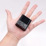
With the advance of GaN technology, high wattage chargers today are getting smaller and smaller. However, there are some chargers which showed us it is still possible to make chargers smaller without the use of GaN, with the Innergie 60C and Lenovo Thinkplus PA65 being two examples. Today we have another compact high wattage charger that we teased earlier that adopts conventional design, the ZMI zPower Turbo 65W USB-C PD charger.
I Design
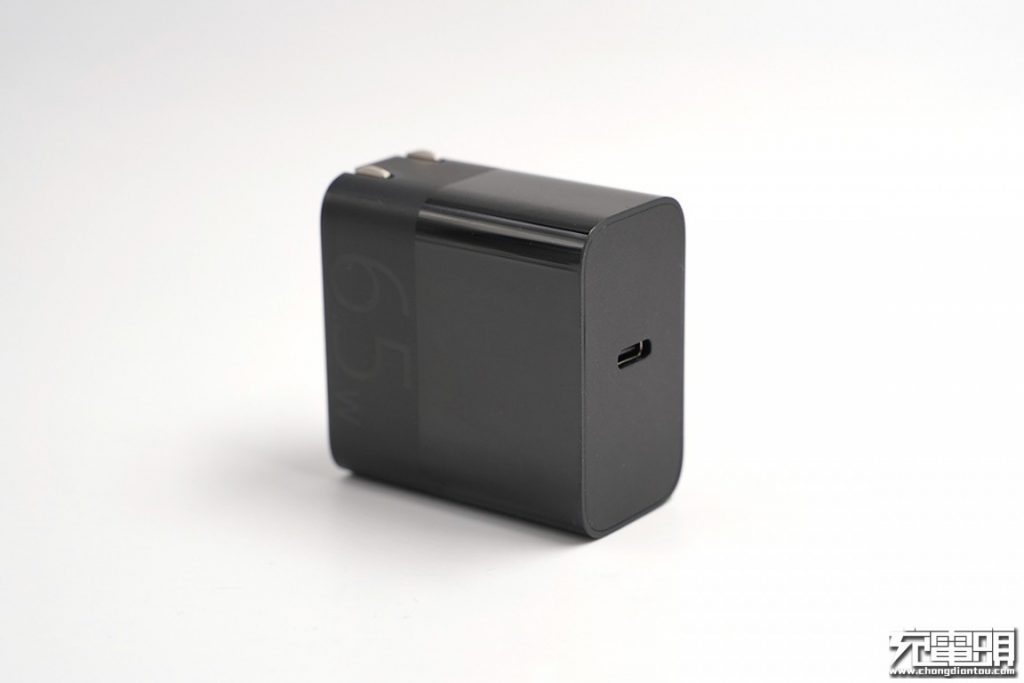
The ZMI 65W charger features a two-tone design with a glossy and matte finish.
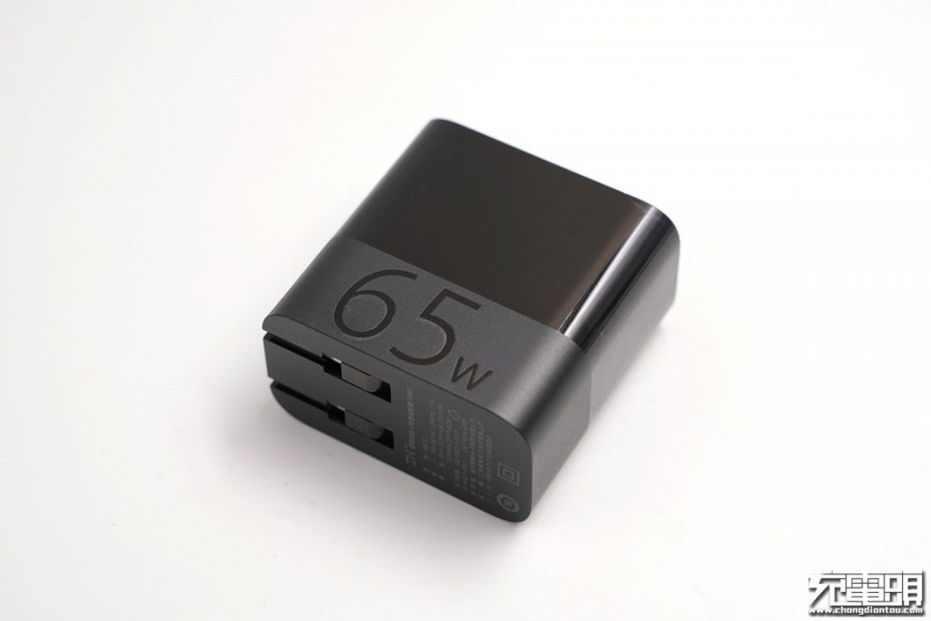
Foldable prongs.
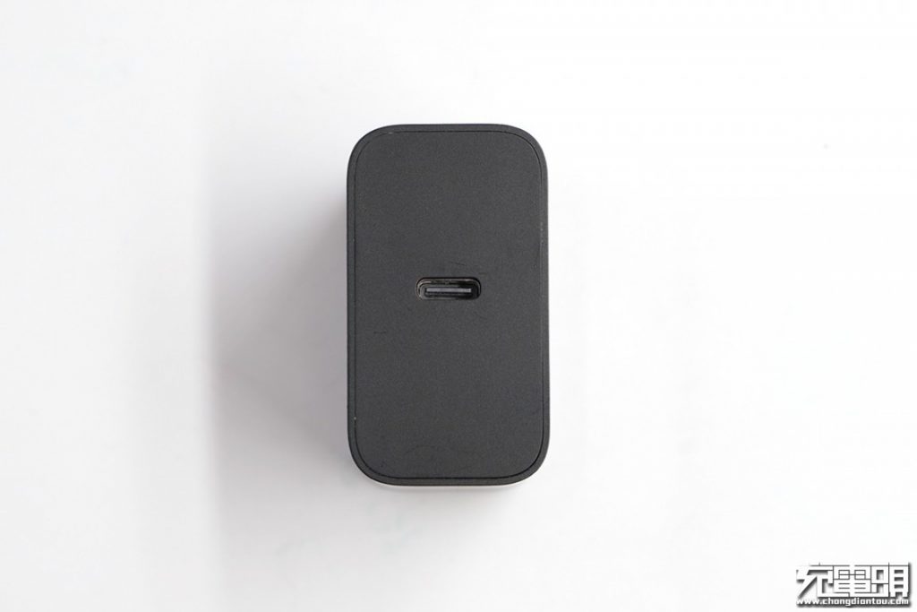
A single USB-C output port.
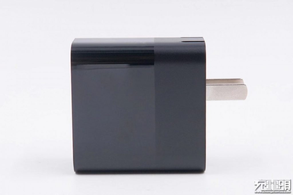
Side view.
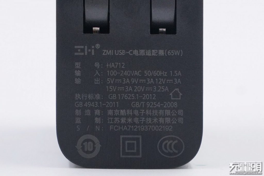
Specifications:Model: HA712
Input: 100~240V AC 50/60Hz 1.5A
Output: 5V/3A, 9V/3A, 12V/3A, 15V/3A, 20V/3.25A
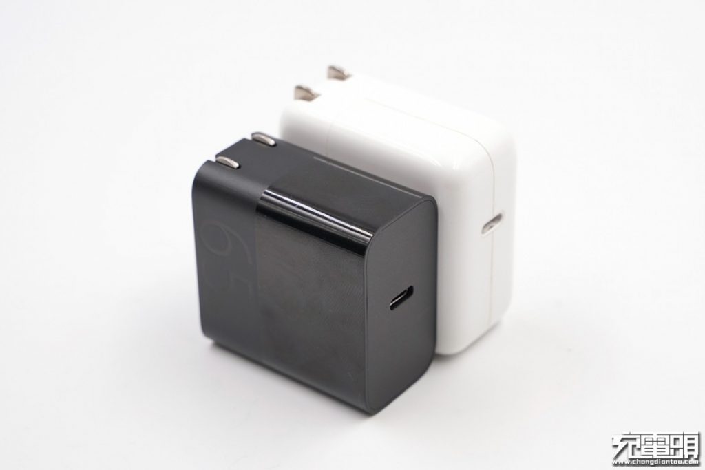
Compared to the Apple 30W PD charger. 65W vs. 30W here.
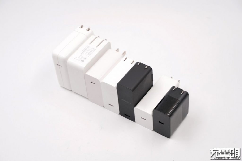
From left to right: Apple 61W, Netease 65W, Huawei 65W, Xiaomi 65W, Lenovo 65W, Lenovo Thinkplus 65W, and ZMI zPower Turbo 65W.
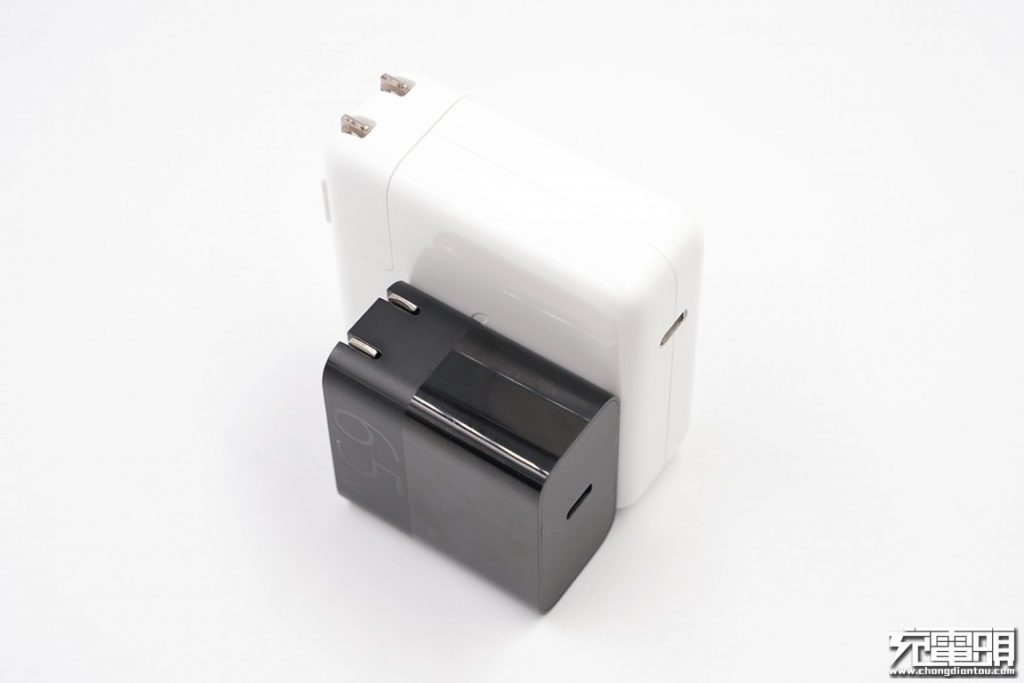
Compared to the Apple 61W PD charger.
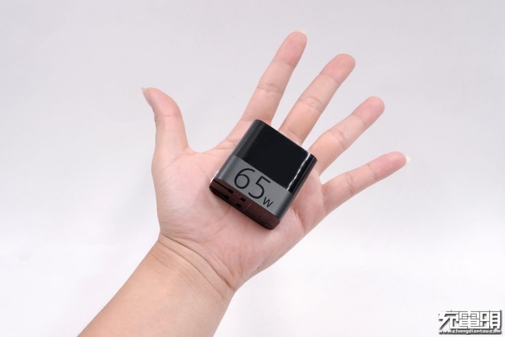
Hands-on.
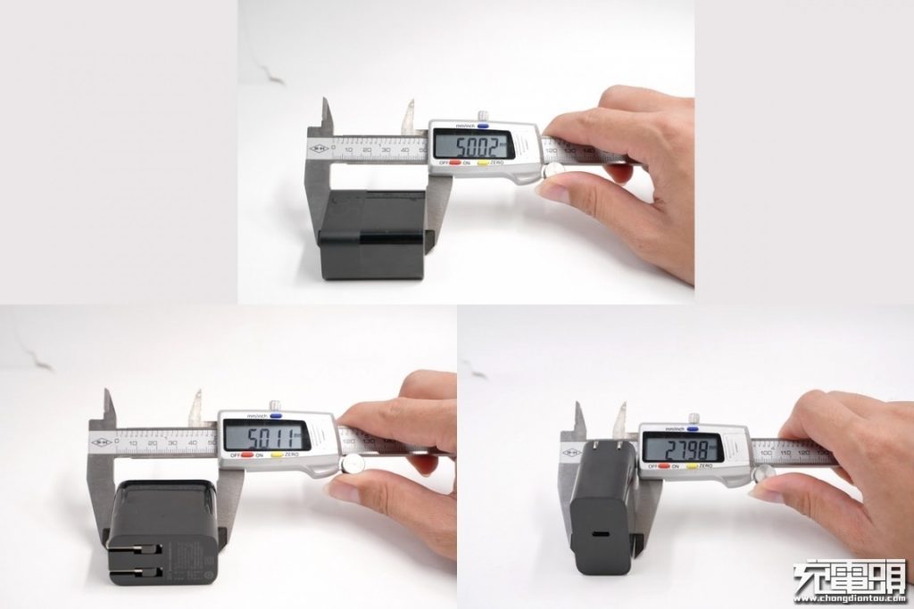
Dimensions: 50*50*28mm (2.0*2.0*1.1in).
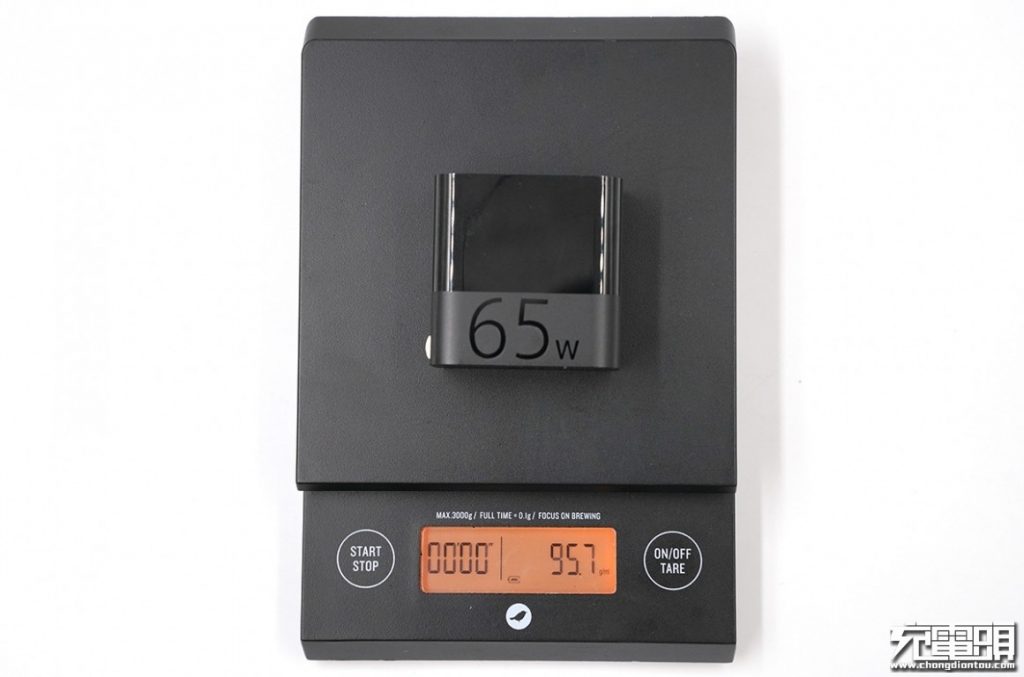
It weighs 95.7g/3.4oz.
II Test
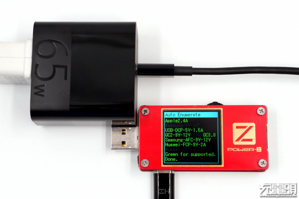
Using ChargerLAB Power-Z KT001 USB power tester, we know that it supports Apple 2.4A, DCP, QC 2.0, QC 3.0, AFC, and FCP protocols.
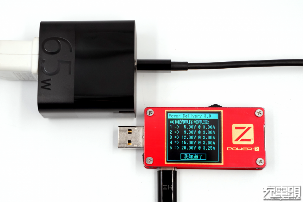
It also supports USB PD 3.0 at 5V/3A, 9V/3A, 12V/3A, 15V/3A, 20V/3.25A.
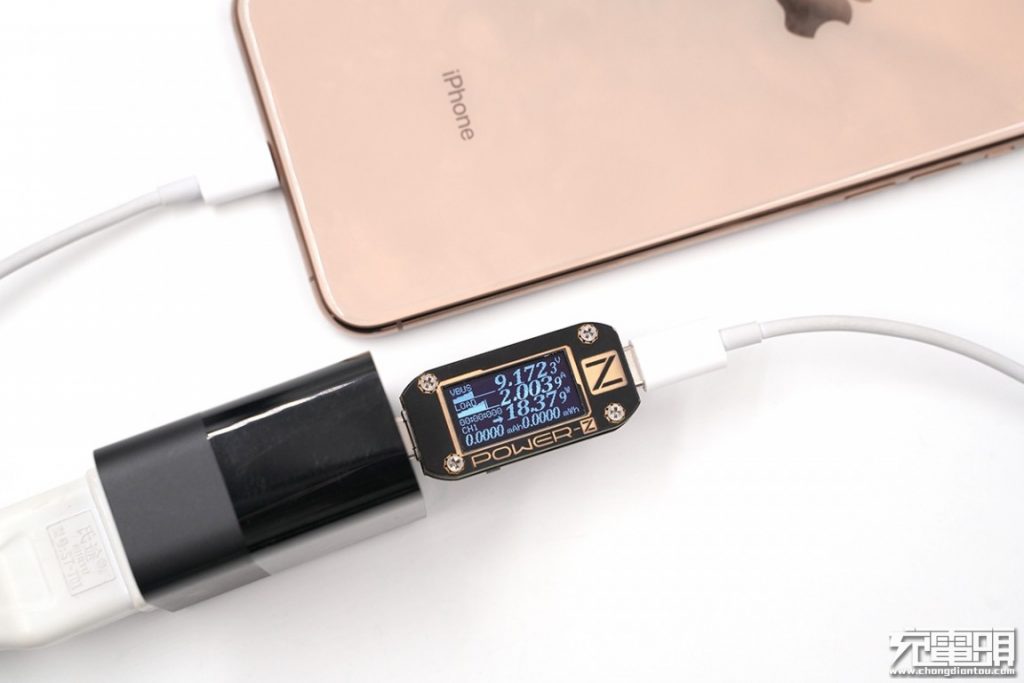
Charging the iPhone XS Max, we are getting 9.17V 2A 18.37W, under PD protocol.
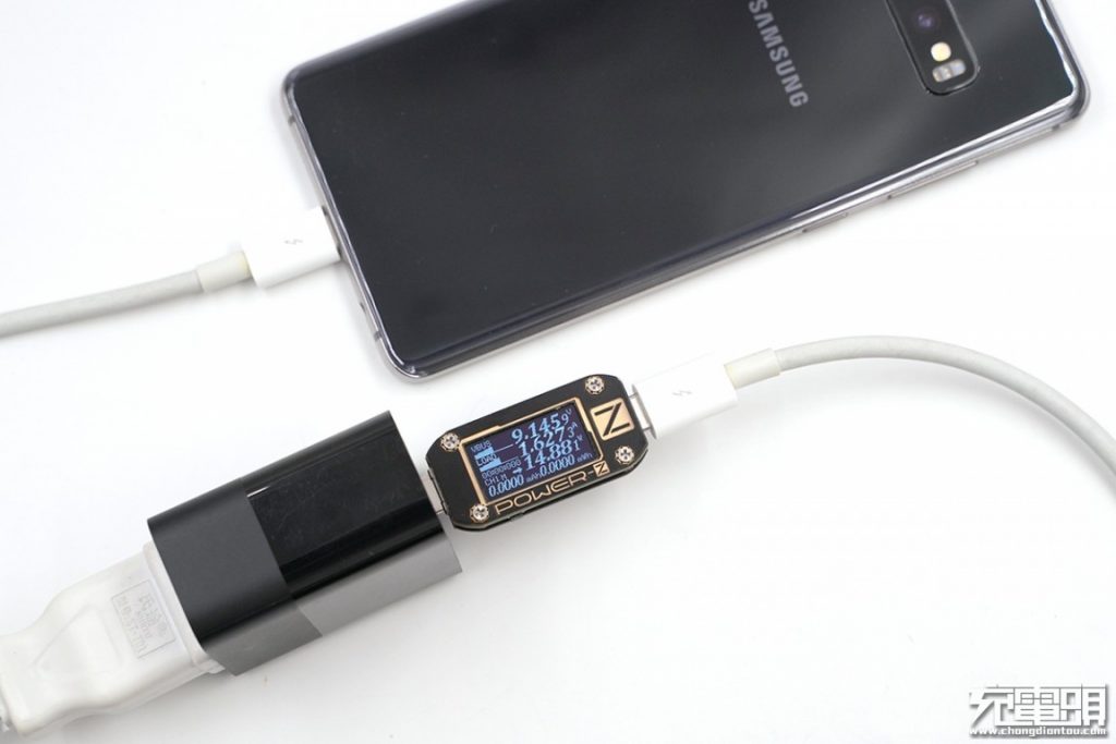
Charging the Samsung Galaxy S10+, we are getting 9.14V 1.62A 14.88W, under PD protocol.
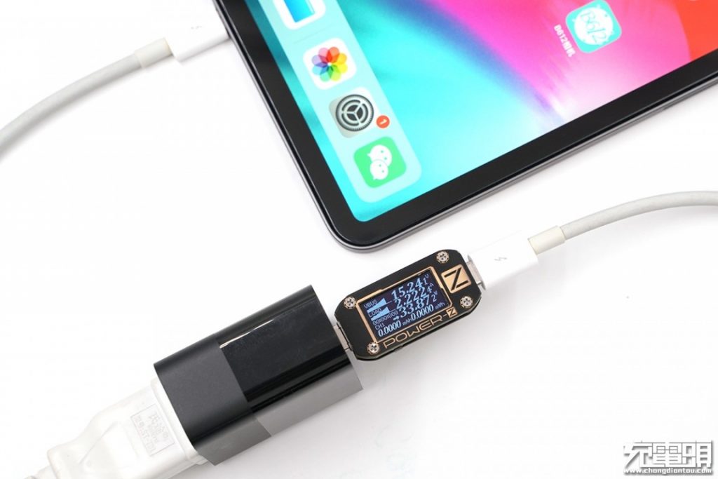
Charging the iPad Pro 11-inch, we are getting 15.24V 2.22A 33.87W, under PD protocol.
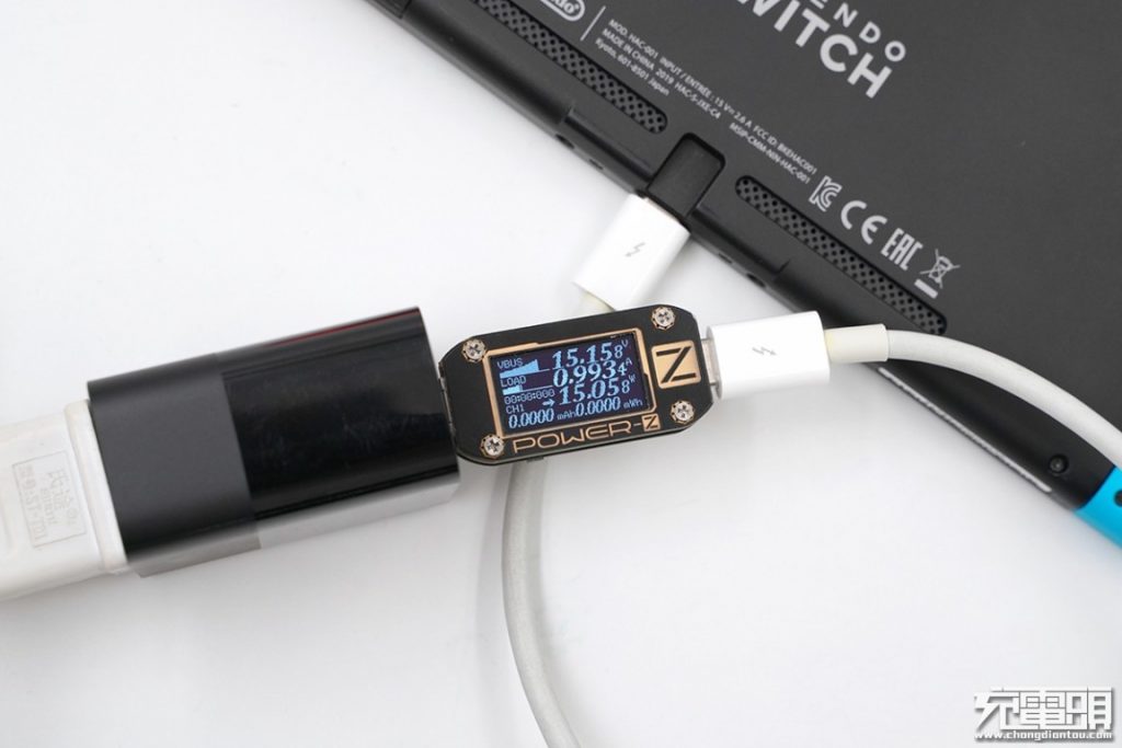
Charging the Nintendo Switch (handheld mode), we are getting 15.15V 0.99A 15.05W, under PD protocol.
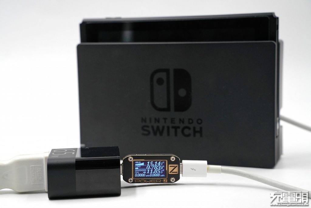
Charging the Nintendo Switch (handheld mode), we are getting 15.15V 0.99A 15.05W, under PD protocol.
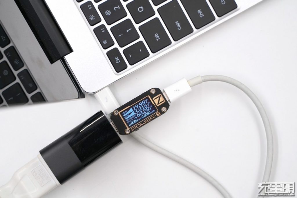
Charging the Huawei MateBook 13, we are getting 19.98V 3.01A 60.28W, under PD protocol.
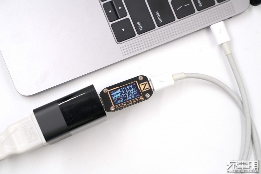
Charging the MacBook Pro Pro 13.3-inch, we are getting 19.99V 2.56A 51.28W, under PD protocol.
III Teardown
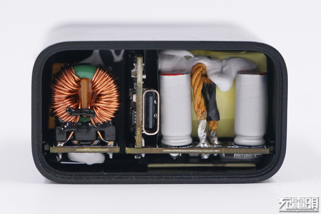
Pry it open from the output panel, the PCBA is tightly attached to the case and cannot be removed directly. You can already tell it's a high quality charger at the glimpse of the inside, if you read a lot of our teardowns.
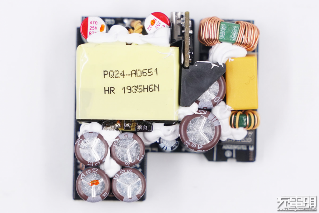
We have to cut the outer casing open to take out the internal PCB board. It can be seen that the layout of the internal PCB board is very tight but organized, with white glue filled between the components. The input end is populated with X capacitors, inductors, time-delay fuses and other components, along with six electrolytic capacitors in two sizes.
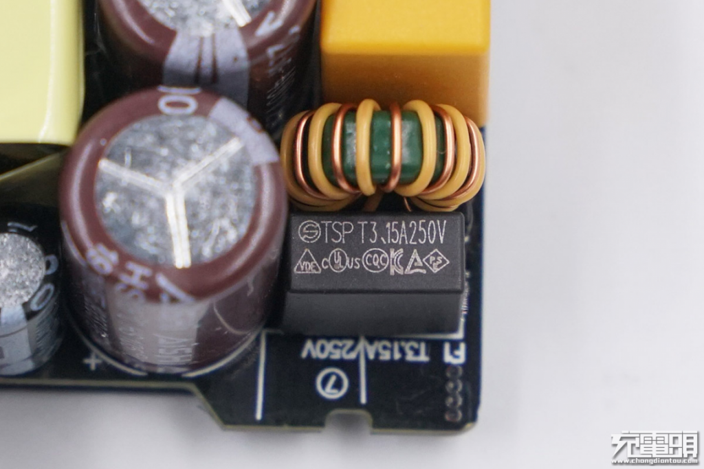
Input delay fuse, 3.15A 250V.
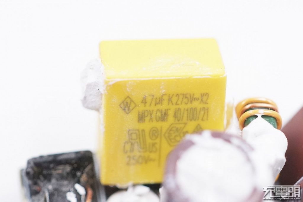
X capacitor, 0.47μF.
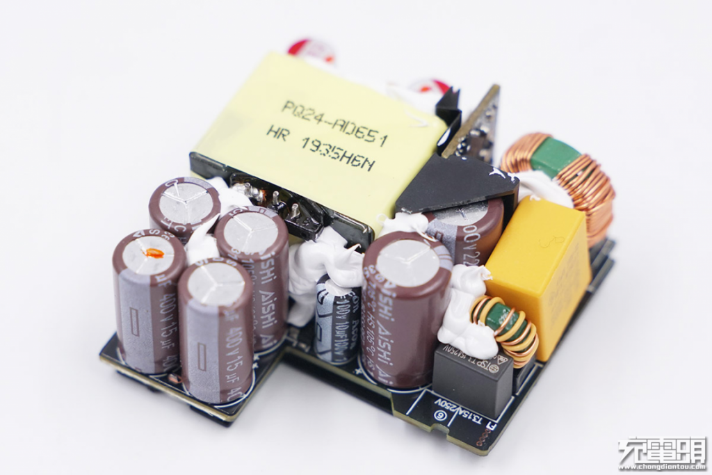
The six electrolytic capacitors are all from the AiSHi (one of China's largest electrolytic capacitor manufacturers).
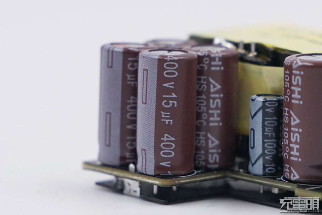
The four smaller electrolytic capacitors, 15μF 400V.
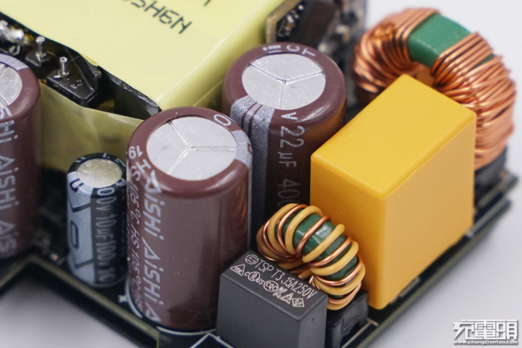
The two larger electrolytic capacitors, 22μF 400V, so the six in a total of 104μF.
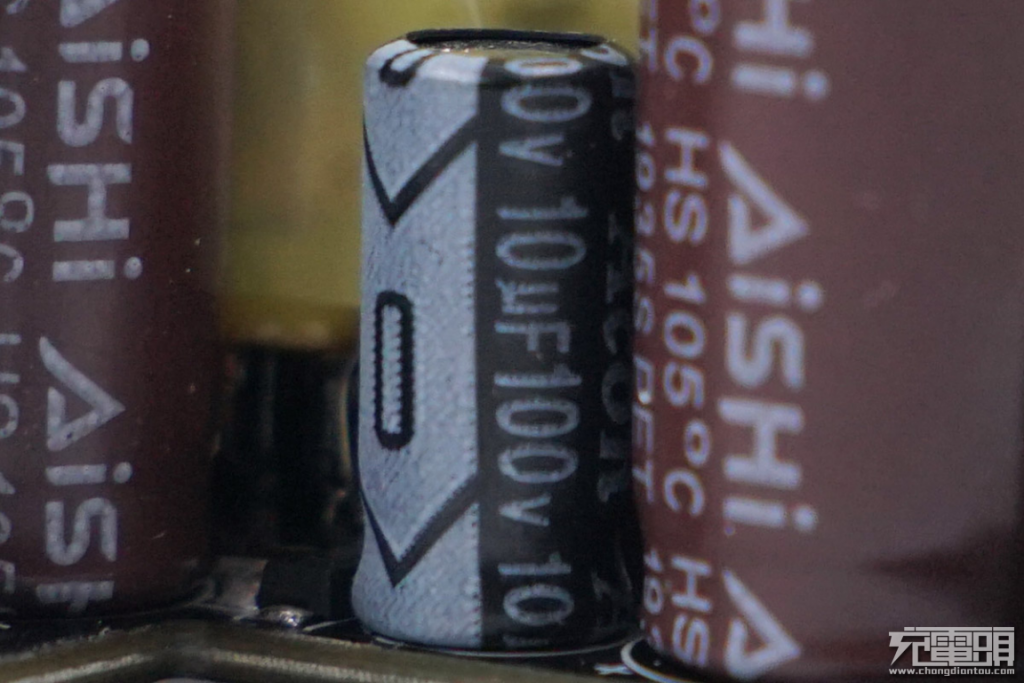
PWM chip power supply capacitor, 10μF 100V.
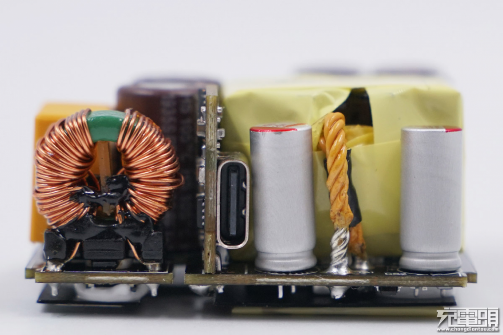
The USB-C port is soldered on a daughter board which is vertically soldered on the main control PCB. The left side PCB board is hollowed out with an extra insulation board (the insulation board is integrated with the outer casing); on the right side are two output filtered solid capacitors.
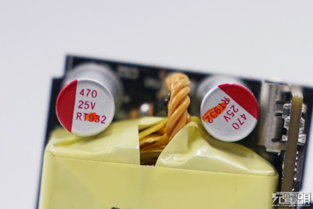
Two solid-state filter capacitors, 470μF 25V, and the transformer uses multiple insulated wires to ensure safety.
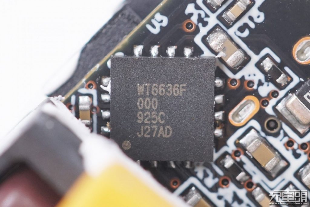
A Weltrend WT6636F is used as the USB-C interface controller. It is a protocol chip (TID No. 1080018) certified by the USB-IF USB PD3.0 (PPS), we have seen it inside the 65W Lenovo Thinkplus "lipstick" charger.
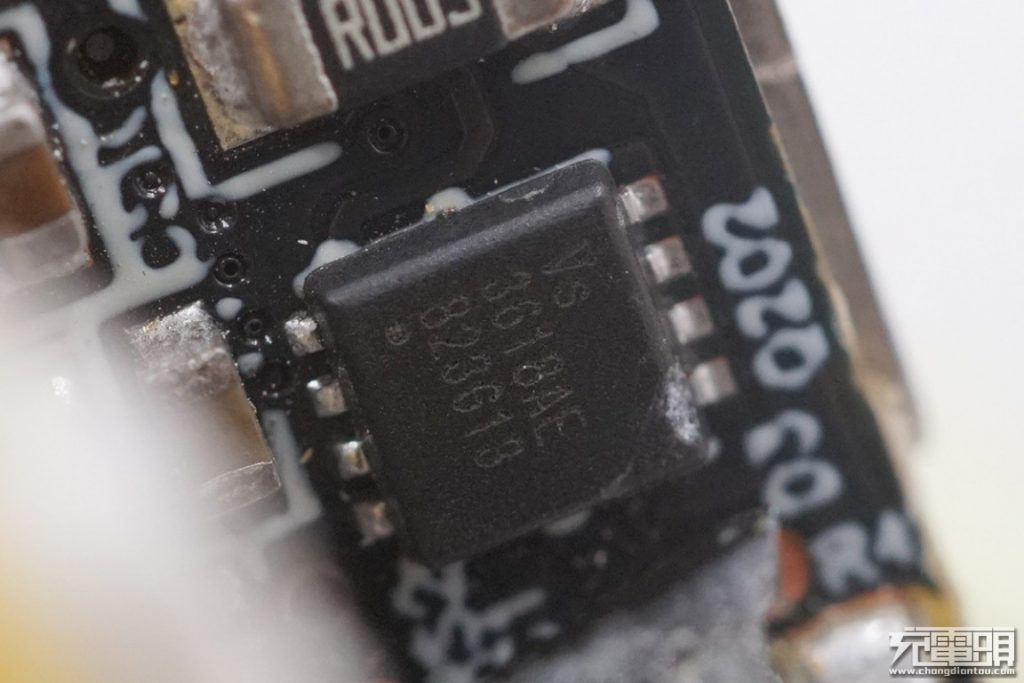
A Vanguard Semiconductor VS3618AE is used as the VBUS switch for USB-C output port.
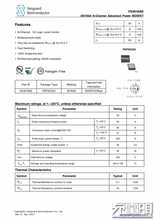
Detailed specifications of the Vanguard Semiconductor VS3618AE.
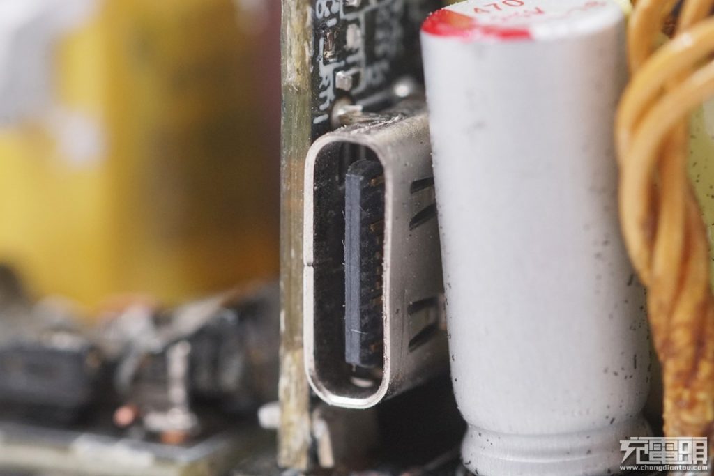
Close-up of the USB-C port.
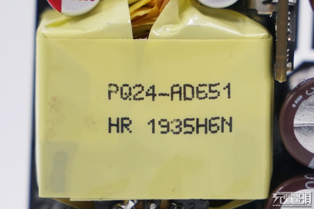
A high quality transformer from HR (one of Delta's main suppliers) with PQ24 core.
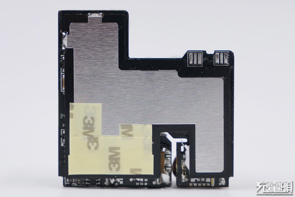
A large metal heat sink is used on the back of the PCB, with a plastic baffle and 3M tape for insulation. There is a hollowed-out design between the primary side and the secondary side.
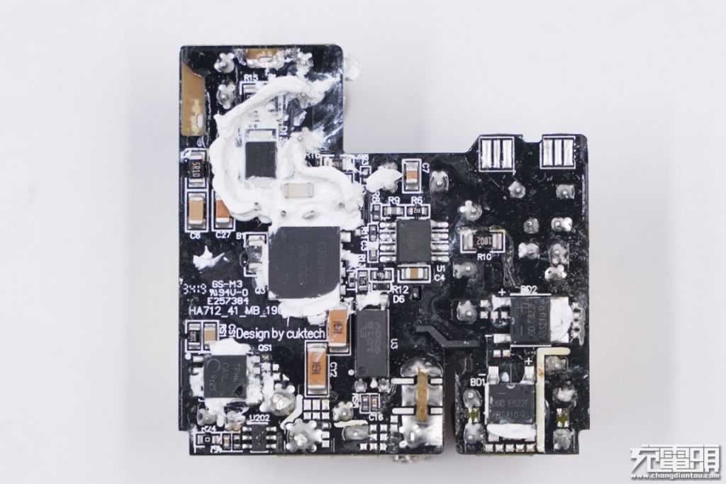
Remove the metal heat sink, it can be seen that the heat-generation components on the PCB are covered with white glue for heat dissipation.
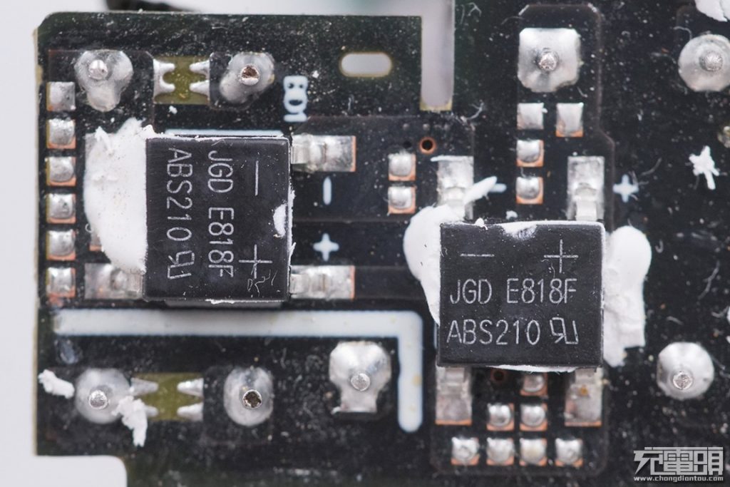
The input side uses two rectifier bridges, which distribute heat to avoid excessive temperature rise.
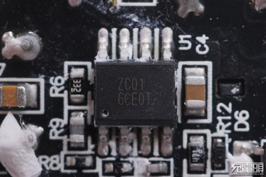
Primary PWM controller chip with letter code ZC01 6CE0T. It is a custom made chip for ZMI, the information about it is yet to be revealed.
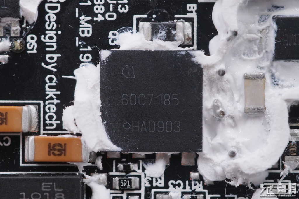
Primary side main control switch, an Infineon's superjunction CoolMOS, model IPL60R185C7, 600V withstand voltage.
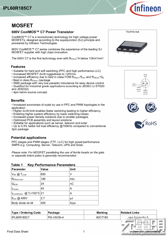

Detailed specifications of the Infineon IPL60R185C7.
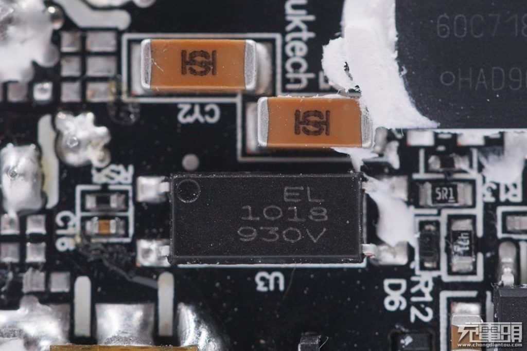
An EL optical optocoupler positioned between the primary and secondary. Above are patch mounted Y capacitors.
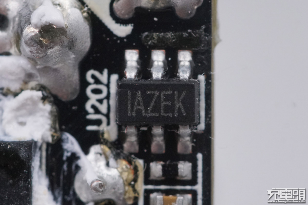
Secondary synchronous rectification controller from MPS, model MP6908.
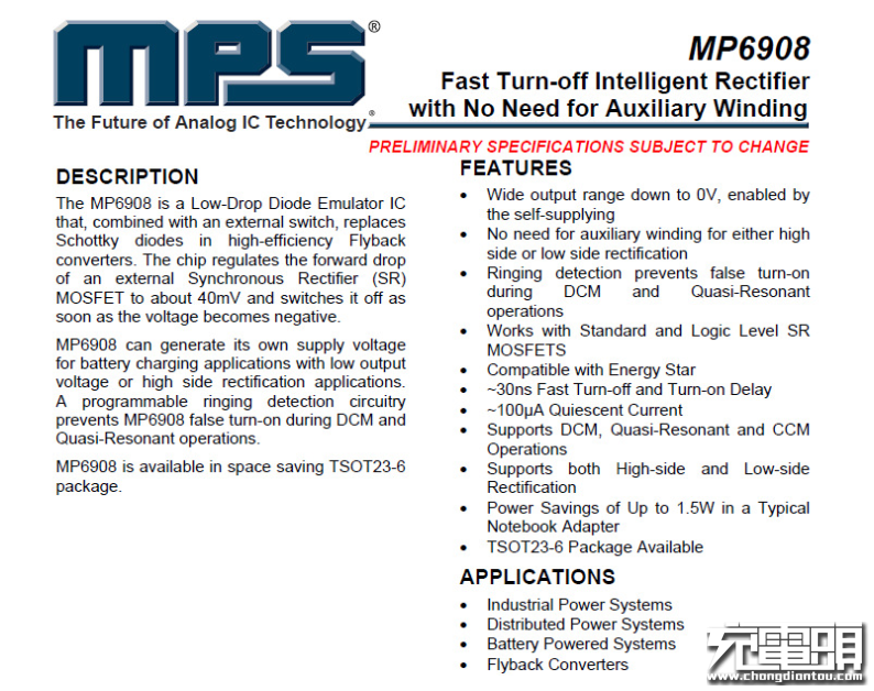
Detailed specifications of the MPS MP6908.
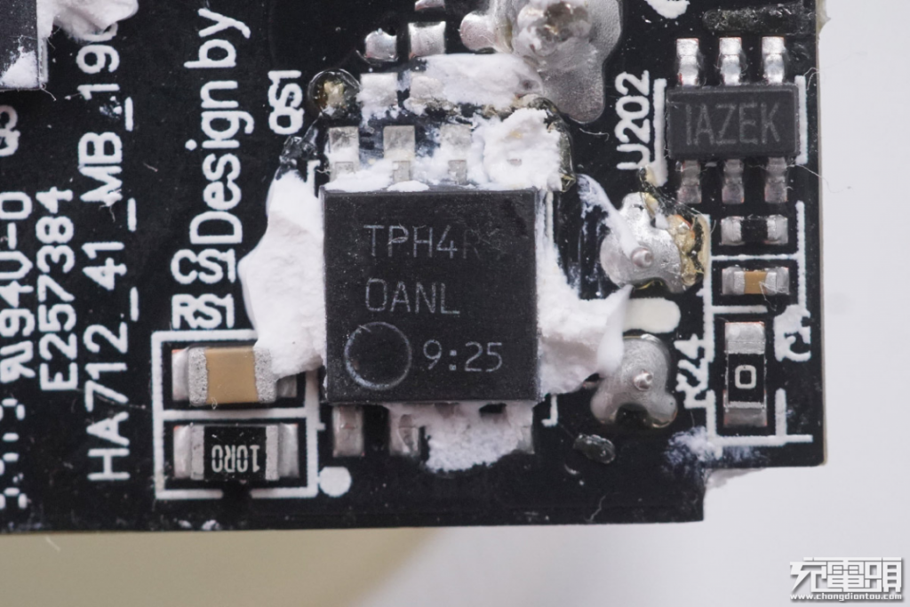
Secondary synchronous rectification MOS tube, Toshiba TPH4R10ANL.
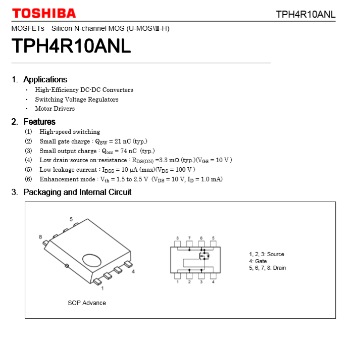
Detailed specifications of the Toshiba TPH4R10ANL.
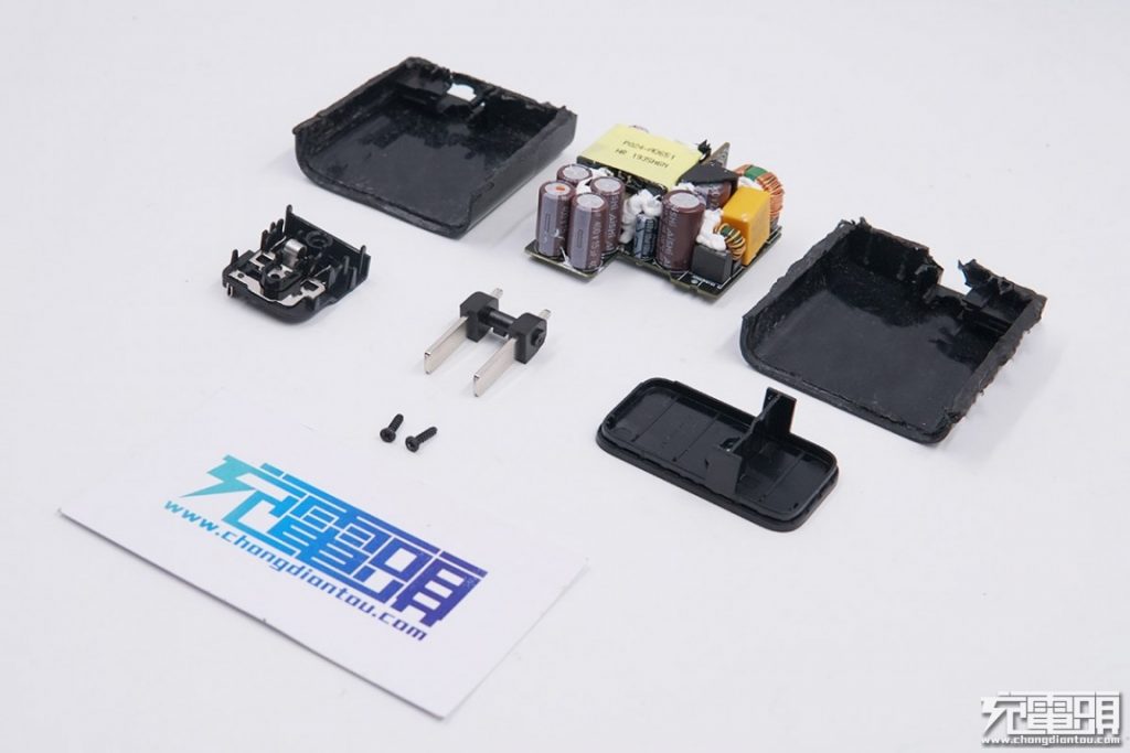
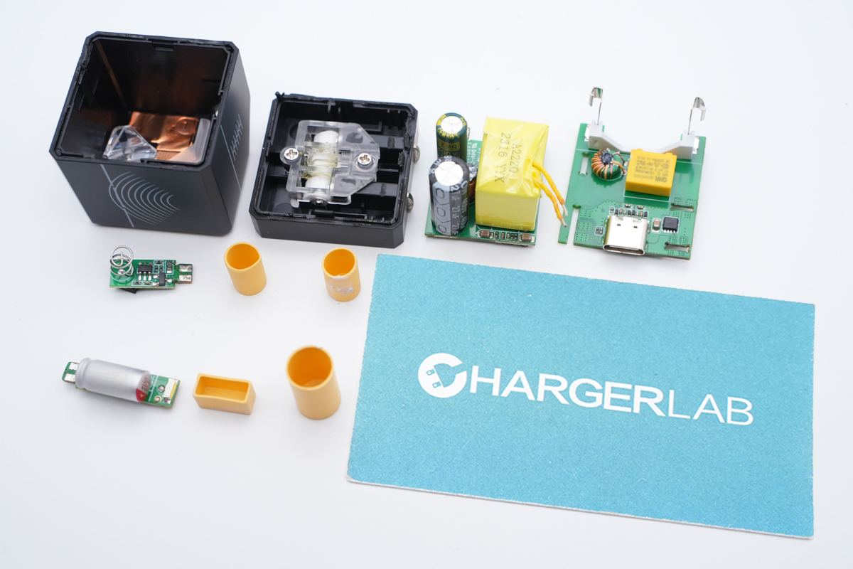
All the components.
IV Conclusion
Design within constraints. The ZMI zPower Turbo 65W USB-C PD charger showed us there is still room for optimization with a conventional charger design. Without GaN, power engineers need to use more components and relatively larger transformer and capacitors for the same performance. However, with a deep understanding of space, performance, and heat dissipation, engineers at ZMI present us a surprisingly balanced charger in term of size, performance, and affordability. Darn impressive.
Pros:
Compact and powerful.
High quality components (even includes an in-house chip).
Affordable.
Cons:
Availablity
Source: chongdiantou

