Introduction
GaN charger is the most frequently mentioned word in our website. We‘ve taken apart many GaN chargers. However, many people may not know what GaN is. Let us talk about it today.
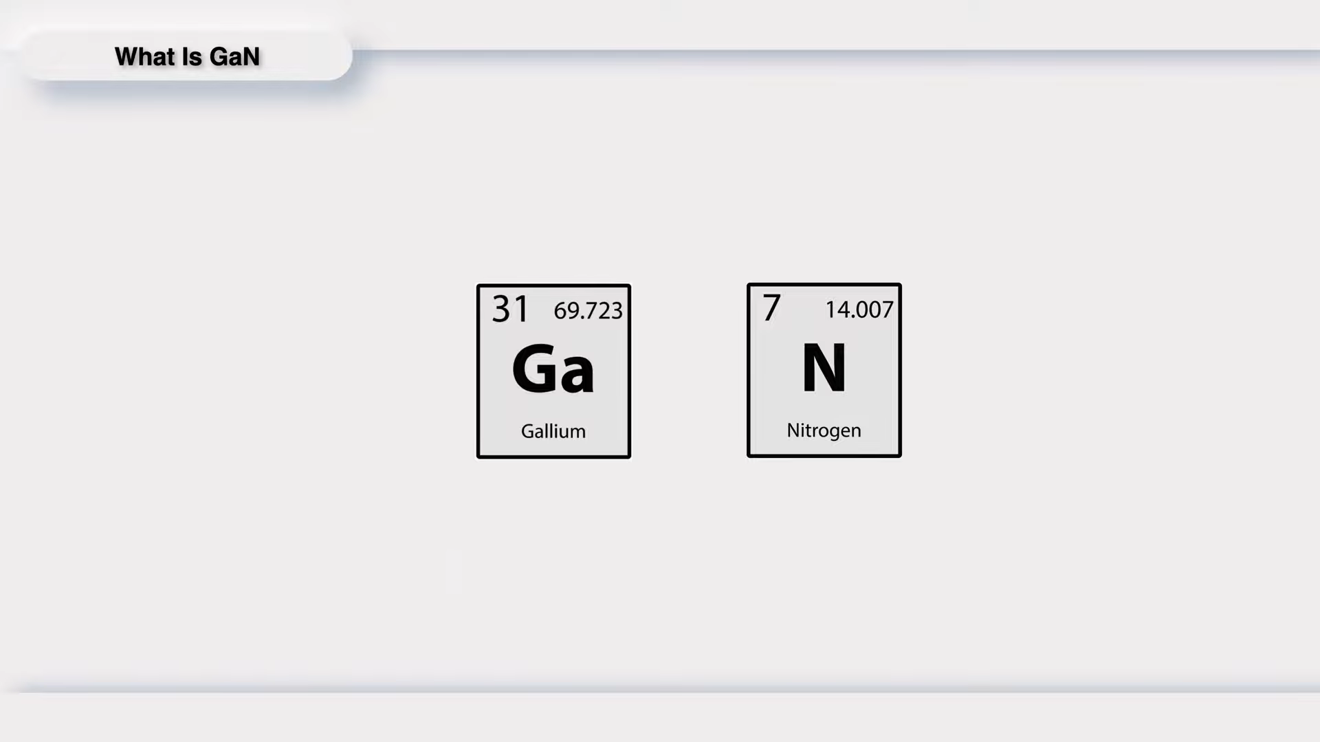
GaN is the abbreviation of Gallium nitride. It's a compound of nitrogen and gallium and is well-known as a third-generation semiconductor material.
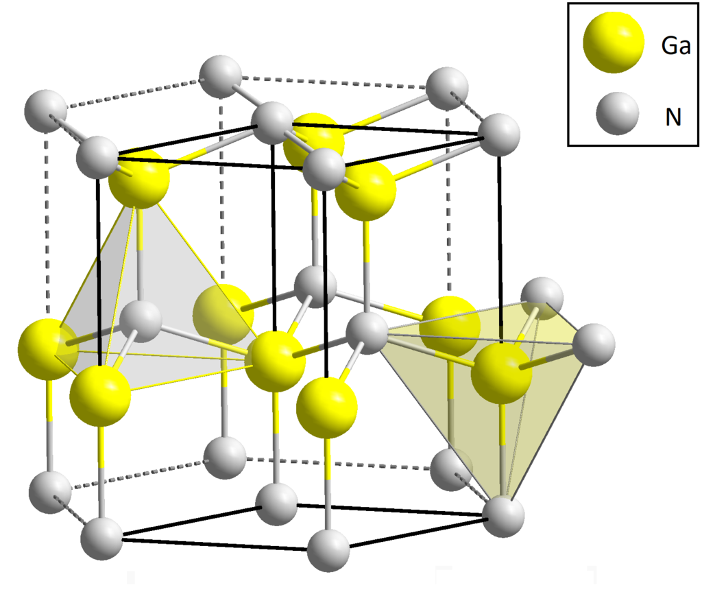
The structure is similar to wurtzite (zinc and iron sulfide mineral) with high hardness.
It also has a very wide band gap of 3.4 eV (electron volts) and can be used in high-power, high-speed optoelectronic components.
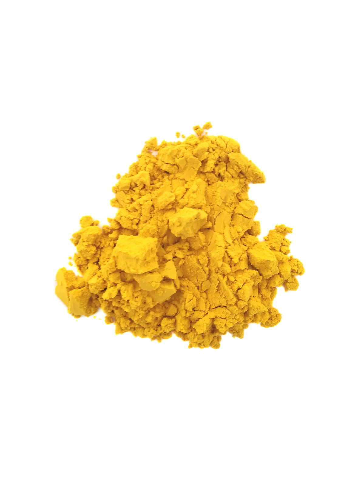
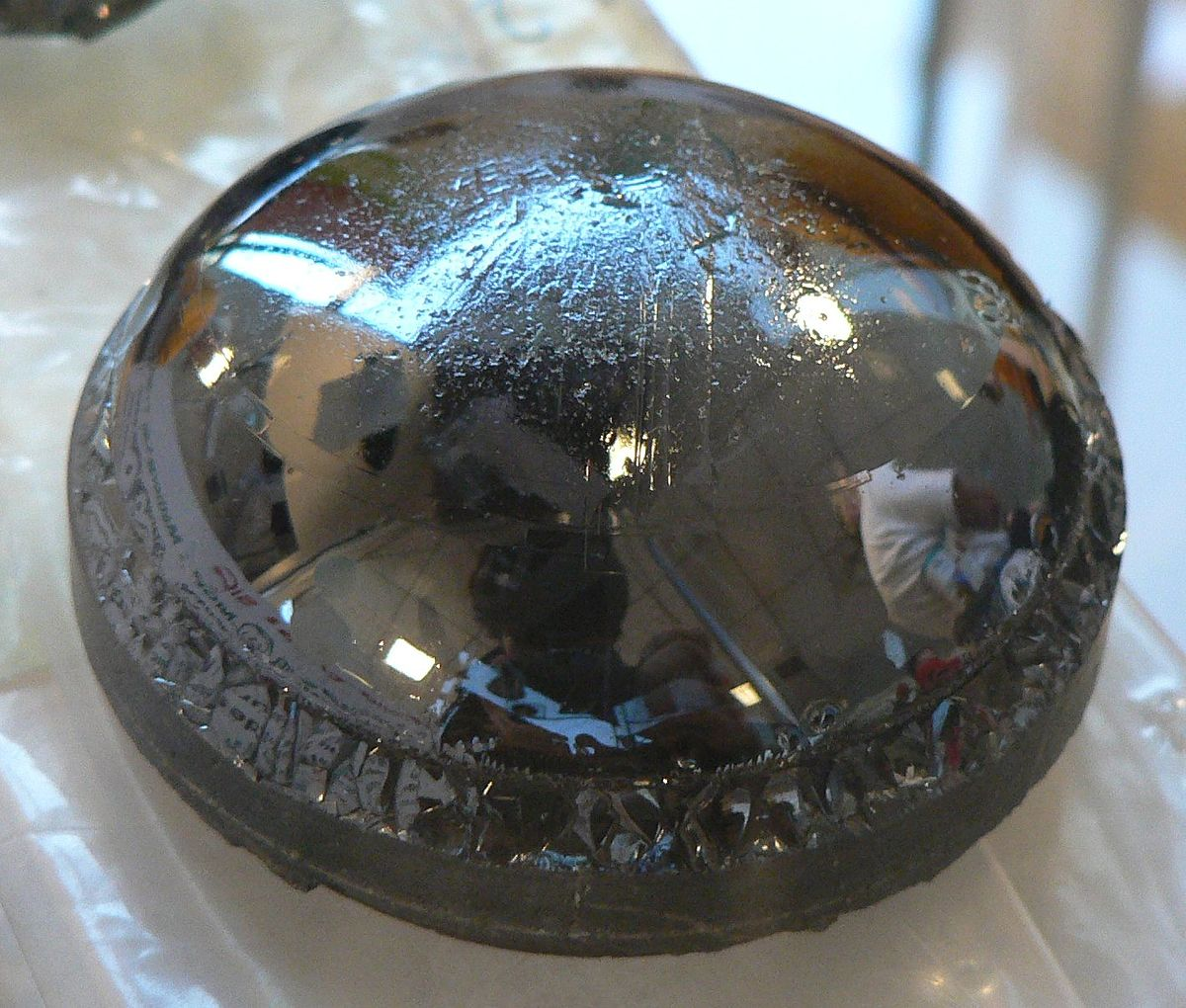
If you look at it from the outside, you will find that it's generally like yellow powder.
It can produce chemical reactions when exposed to water and is non-flammable.
The compound was first synthesized in 1928. After 70 years of continuous development, it was widely used in diodes in the 1990s.
The performance of GaN switch transistors is much better than that of silicon-based switch transistors, which is mainly reflected in the following five aspects:
1. Higher breakdown voltage
2. Faster switching frequency
3. Lower on-resistance
4. Higher thermal conductivity
5. Lower switching losses
Furthermore, it can be grown on a variety of substrates, including sapphire, silicon carbide (SiC), and silicon (Si).
So, it can achieve higher efficiency, higher power density, or even both after replacing silicon components with GaN components.
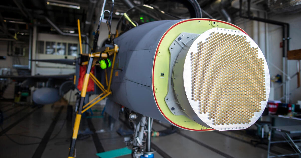
For now, GaN components are widely used in many fields. For example, GaN semiconductors can be used in military electronics industry. It's now the first choice for producing large-scale search radars for fighter aircraft.
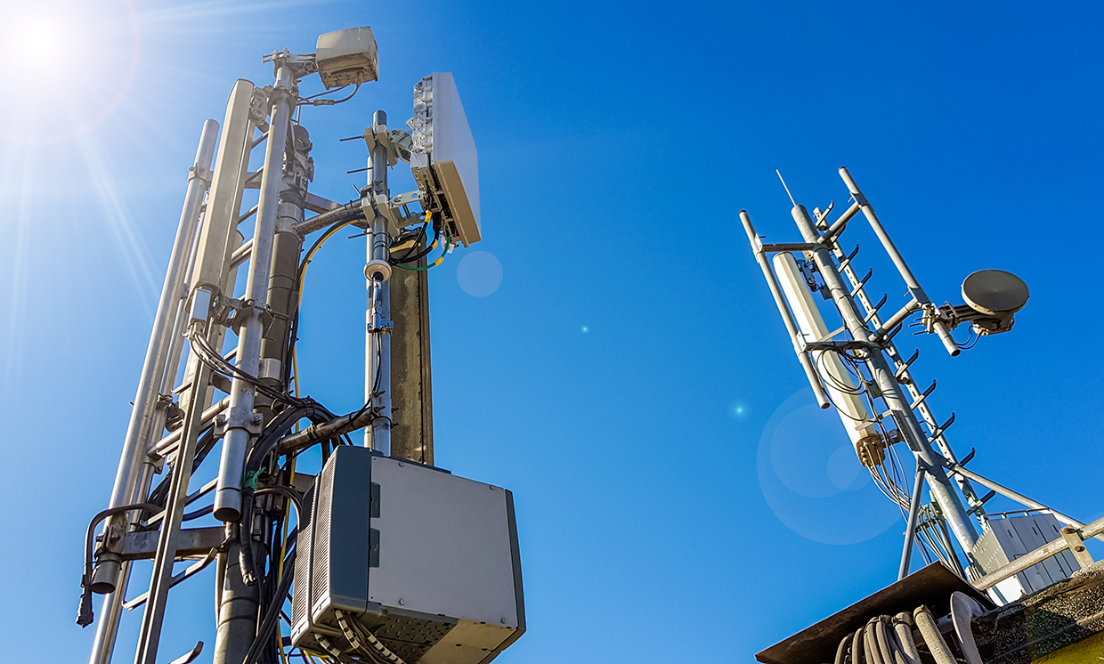
And it can also be used in base stations. The higher energy efficiency, wider bandwidth, higher power density, and smaller size make it ideal for next-generation base stations, especially in the frequency band above 1.8GHz.
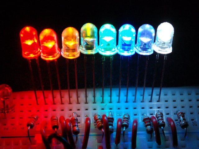
In the field of optoelectronics, GaN is used to make LEDs and lasers. GaN can be mixed with indium (InGaN) or aluminum (AlGaN) to create LEDs with colors ranging from red to ultraviolet. And the GaN-based violet laser diodes are used to read Blu-ray discs.
But in ChargerLAB, what we are most concerned about is how it is used in chargers.
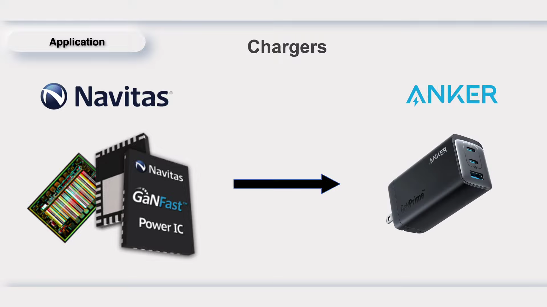
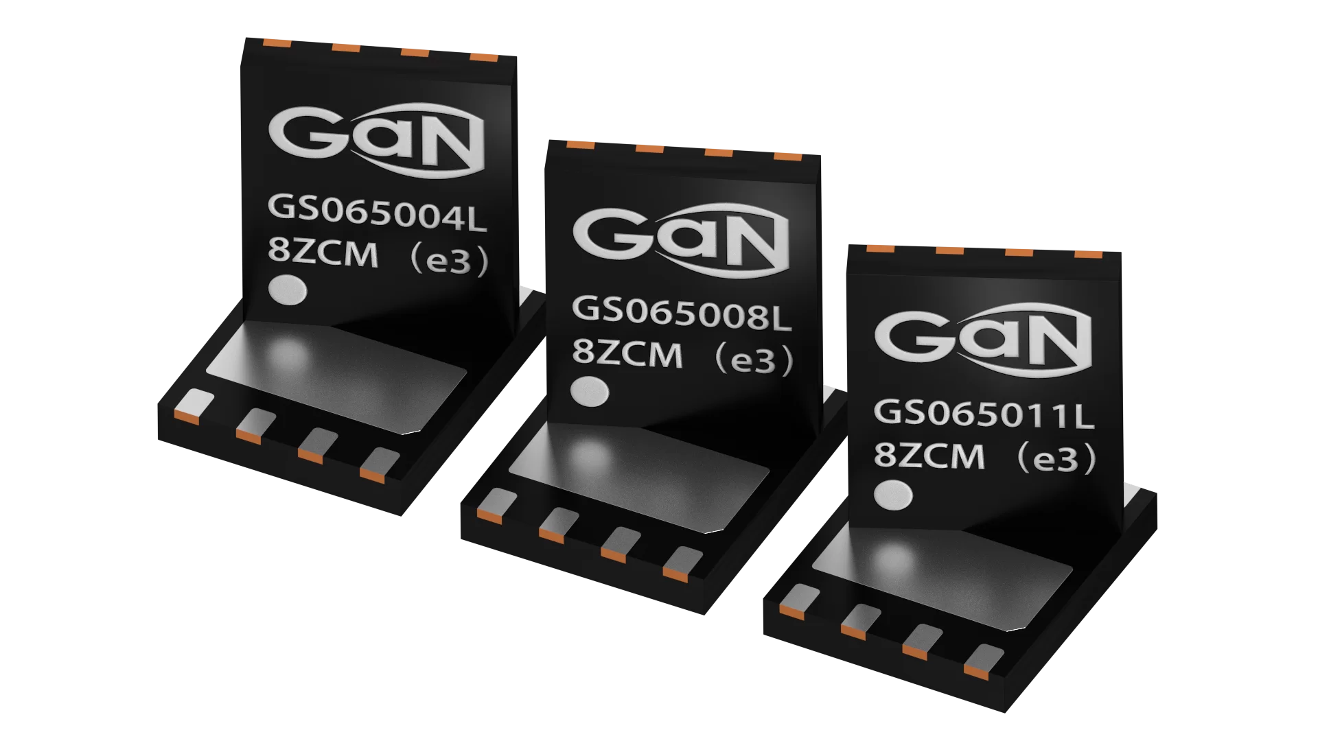
It's not very long for GaN components to be used in chargers. Back in 2014, Navitas, which was just founded, launched the world's first GaN power IC prototype. In 2018, it was first adopted by Anker in their chargers.
Then, more and more manufacturers began to do so, and even Apple launched its first 140W GaN charger.
So how does GaN allow chargers to significantly reduce size and increase output power?
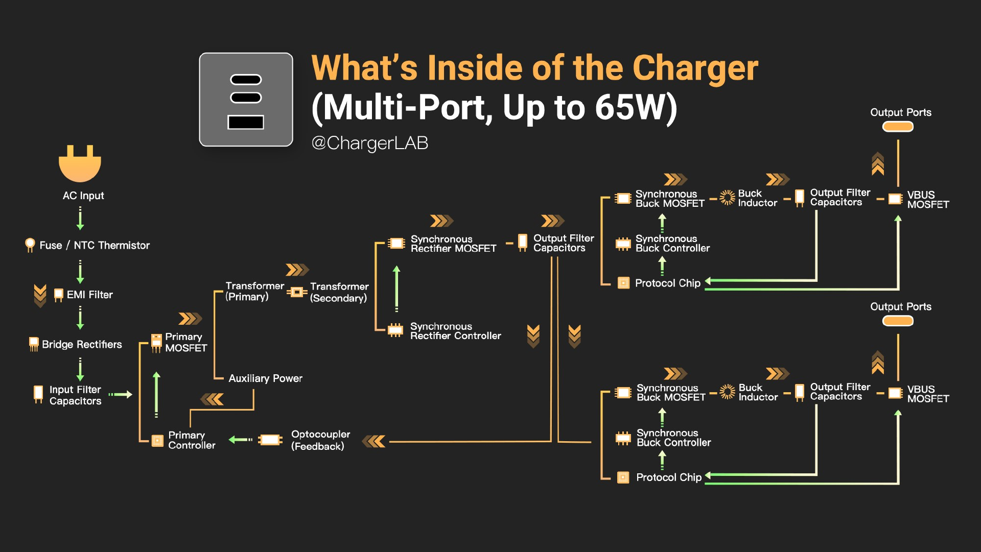
First, we need to understand how the charger works.
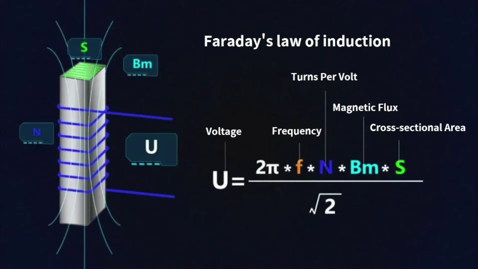
In most cases, the transformer is the largest component in the charger. When the output power is fixed, its size is directly related to the frequency of the pulsed current, that's "f". When the voltage (U) remains unchanged, if we want to reduce the size, that is, reduce the cross-sectional area (S).
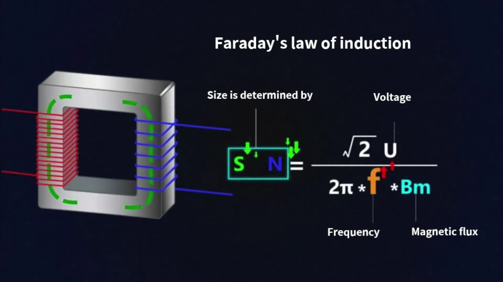
The best way is to increase the frequency (f).
And switch transistor can control the frequency. In the process of continuous switching, the GaN switch transistor can reach higher frequencies than the silicon transistor. The loss is lower and the heat dissipation efficiency is higher. So, the charger and transformer can be smaller than before.
The charger is just a device that can convert high-voltage AC into low-voltage DC.
Switching transistors are the most common components in chargers. When used with capacitors and inductors, they can be used in rectifier circuits, buck circuits, and PFC circuits.
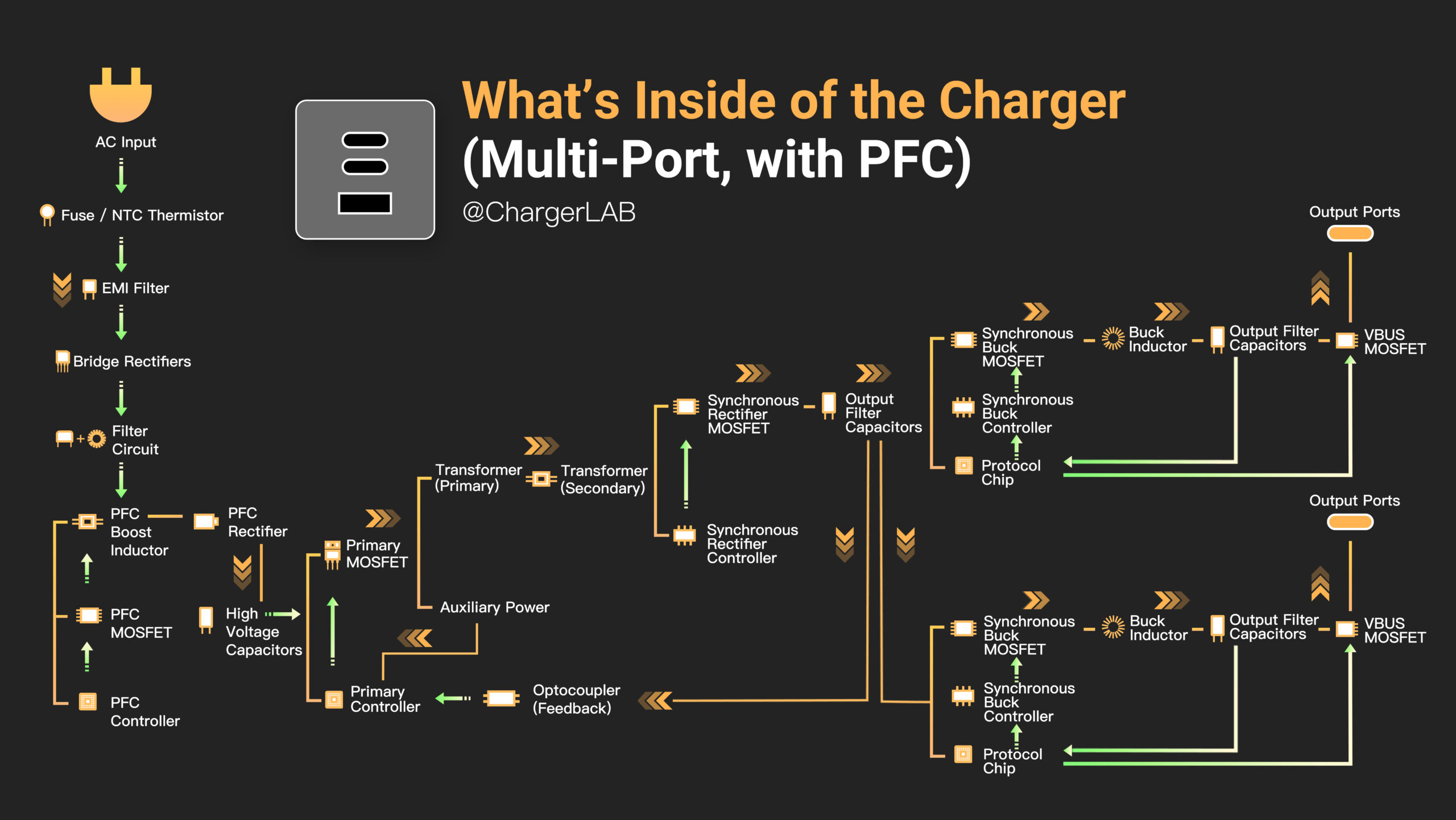
The primary MOSFET and PFC MOSFET are gradually being replaced by GaN components. Some chargers also adopt GaN components to replace synchronous rectification MOSFET, like the Anker GaNPrime series. The synchronous buck MOSFET and VBUS MOSFET may also be gradually replaced by GaN components in the future.
Summary of ChargerLAB
In conclusion, GaN (gallium nitride) has revolutionized charger technology with its efficiency and compactness. As we look to the future, GaN is poised to play a central role in charger applications, promising even faster charging and smaller form factors. However, the relentless pace of innovation suggests that there may be more advanced materials on the horizon, waiting to take GaN's place. While GaN has certainly left its mark, the charger landscape is an evolving one, and we can anticipate exciting developments in the quest for more efficient and sustainable power solutions.
Related Articles:
1. What Is HDMI? (From 1.0 to 2.1) - ChargerLAB
2. What is USB-C? All you need to know! - ChargerLAB Explained
3. What Is GaN Charger And How It Works? - ChargerLAB Explained (Video)