Introduction
Ever since the charging power of the iPhone increased to 20W and Apple stopped including chargers with their phones, it has ignited the market for 20W fast chargers. Although this move has benefited many third-party accessory manufacturers, Apple's original chargers still dominate in terms of sales. We have previously took apart this charger, you can click the links to have a look.
Recently, Apple released a new 20W charger with the model updated to A2940. However, the most essential difference compared to the older version lies in the master control chip. Interested in learning more? Let's delve into the details below.
Product Appearance
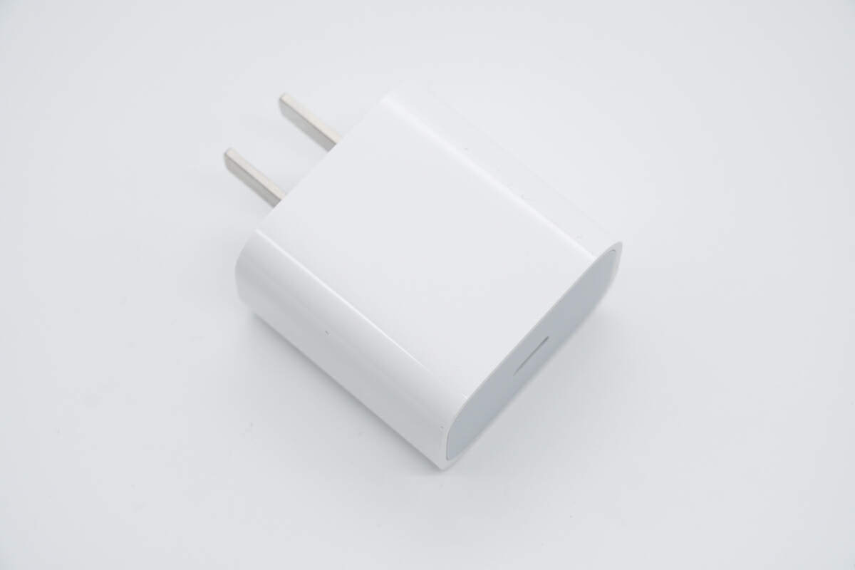
The appearance of the charger still adopts Apple's consistent design – a glossy white shell with a gray bottom end.
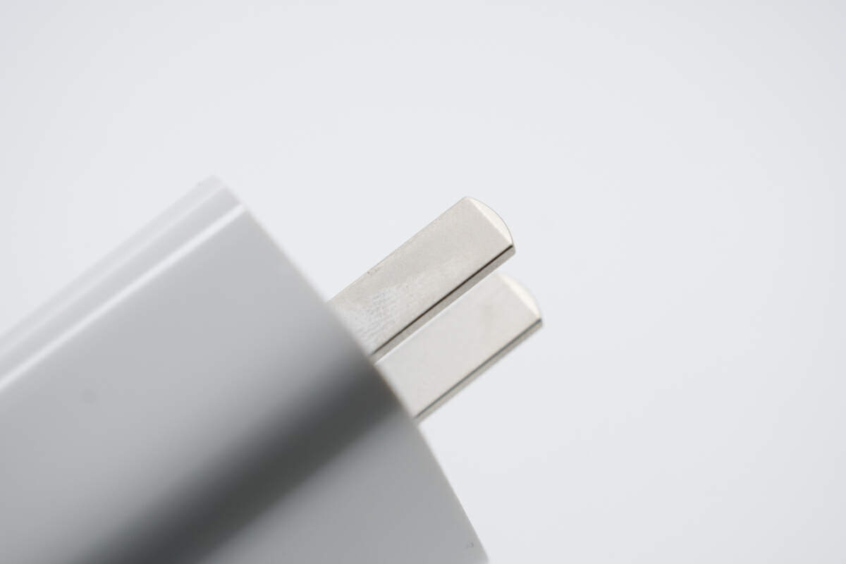
And the input prongs are still not foldable.
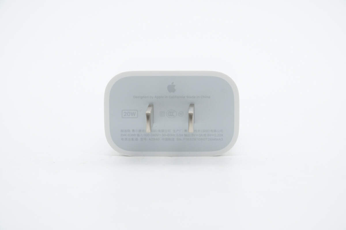
The specs info printed near the prongs tells us it's a new Apple 20W charger.
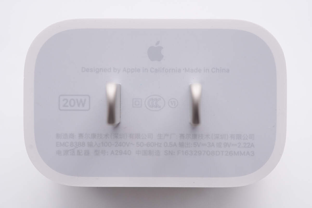
Model is A2940. It supports input of 100-240V~50/60Hz 0.5A, and it also supports output of 5V3A or 9V2.22A. The manufacturer is Salcomp.
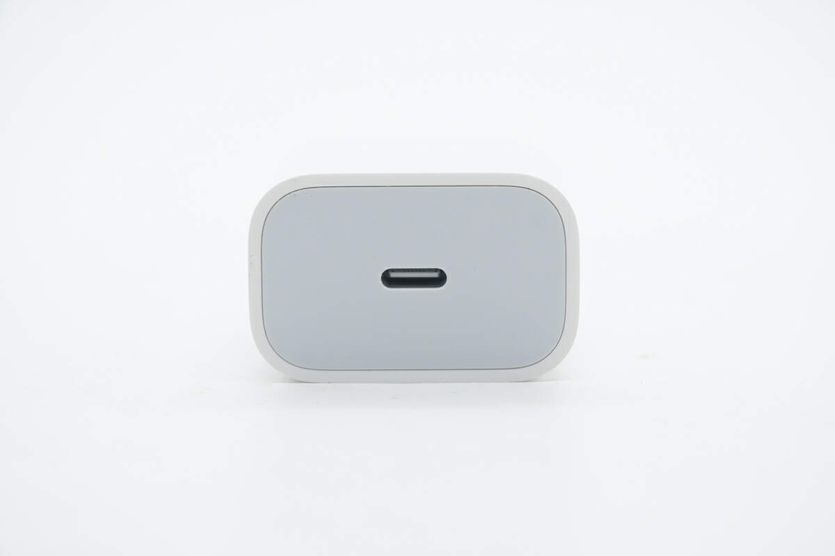
Here is the USB-C port on the top.
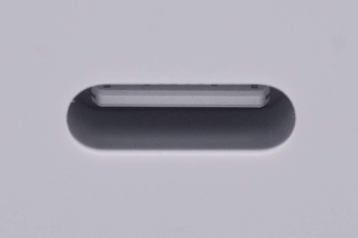
The plastic sheet inside it is white as usual.
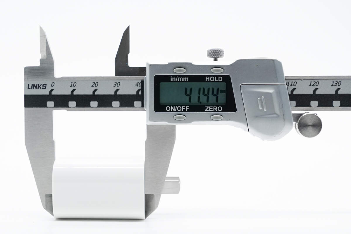
The length of the charging cube is about 41mm (1.61 inches).
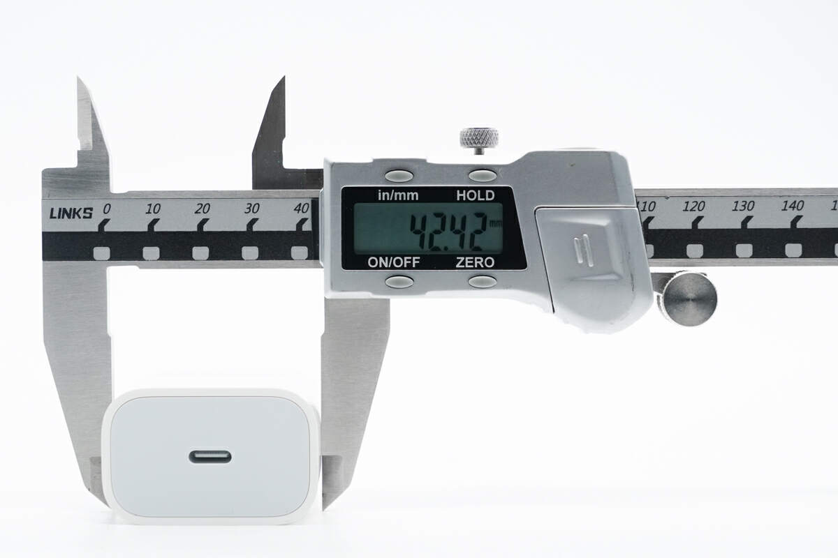
The width is about 42mm (1.65 inches).
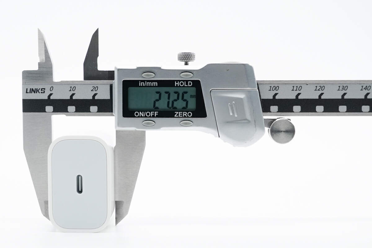
And the height is about 27mm (1.06 inches).
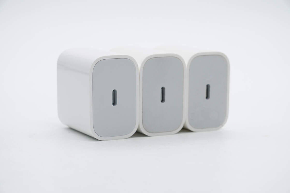
Compared to Apple's previous 20W (middle) and 18W charger (right), when disregarding minor data differences due to non-standard measurements, all three chargers have the same physical size.
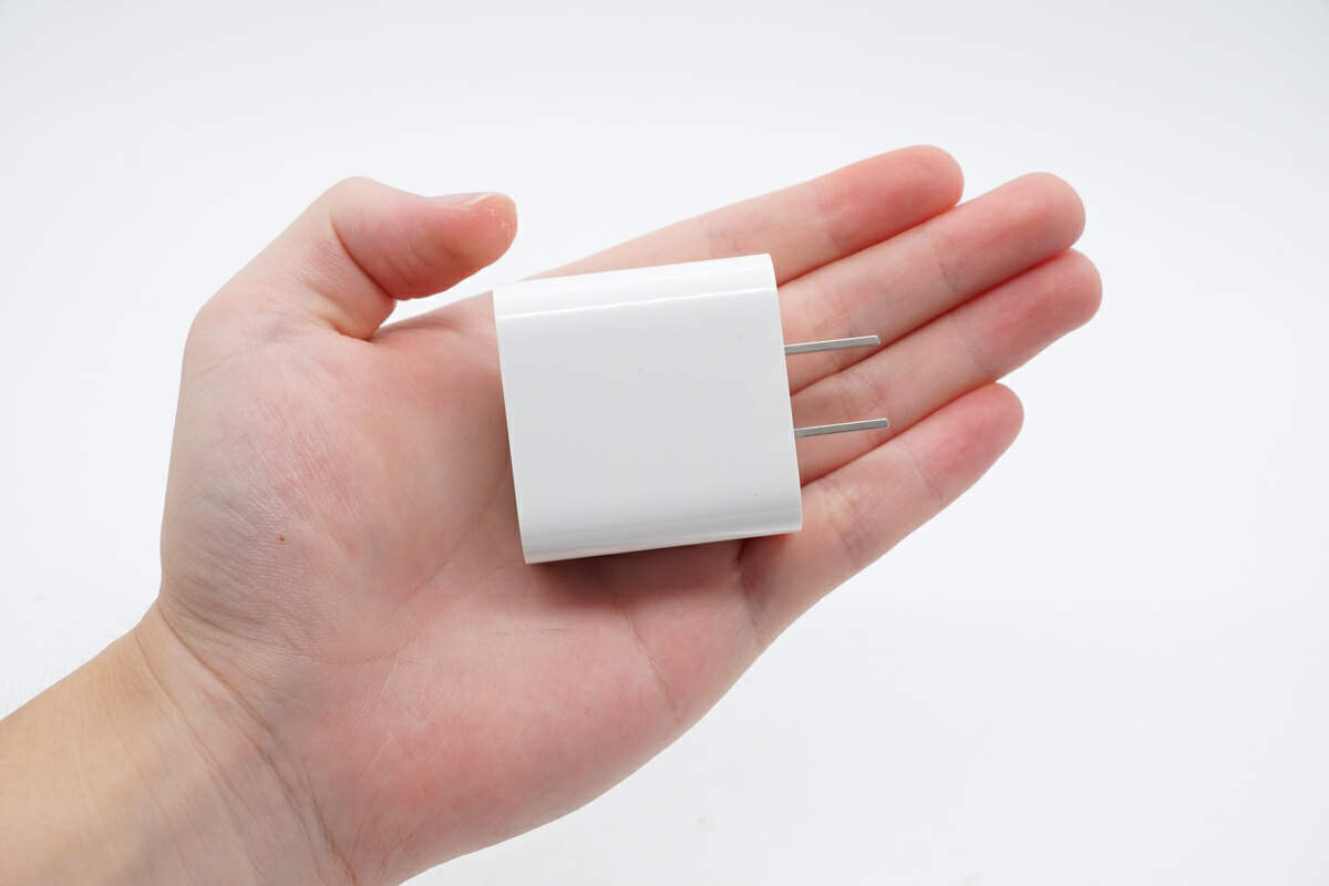
Here's how the charger looks when held in my hand.
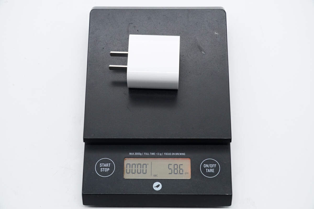
And the weight of this charger is about 59g (2.08 oz).
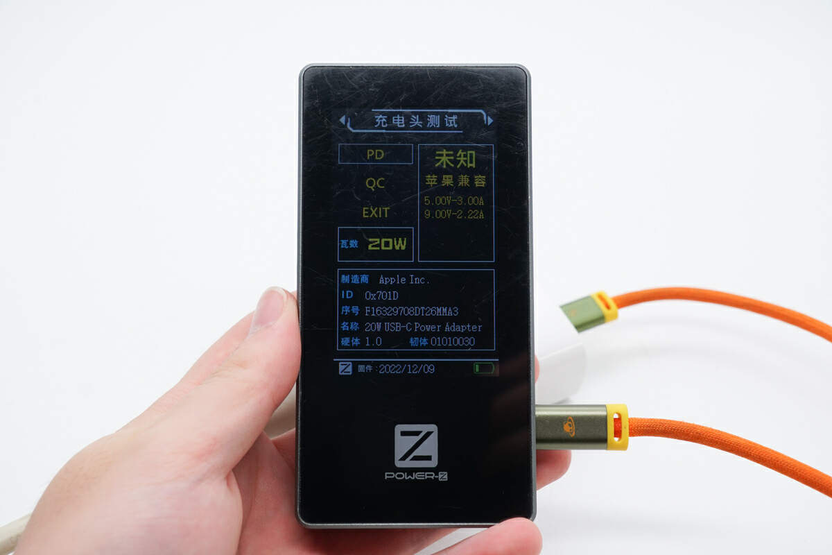
ChargerLAB POWER-Z MF001 identified the serial number of this charger as F16329708DT26MMA3.
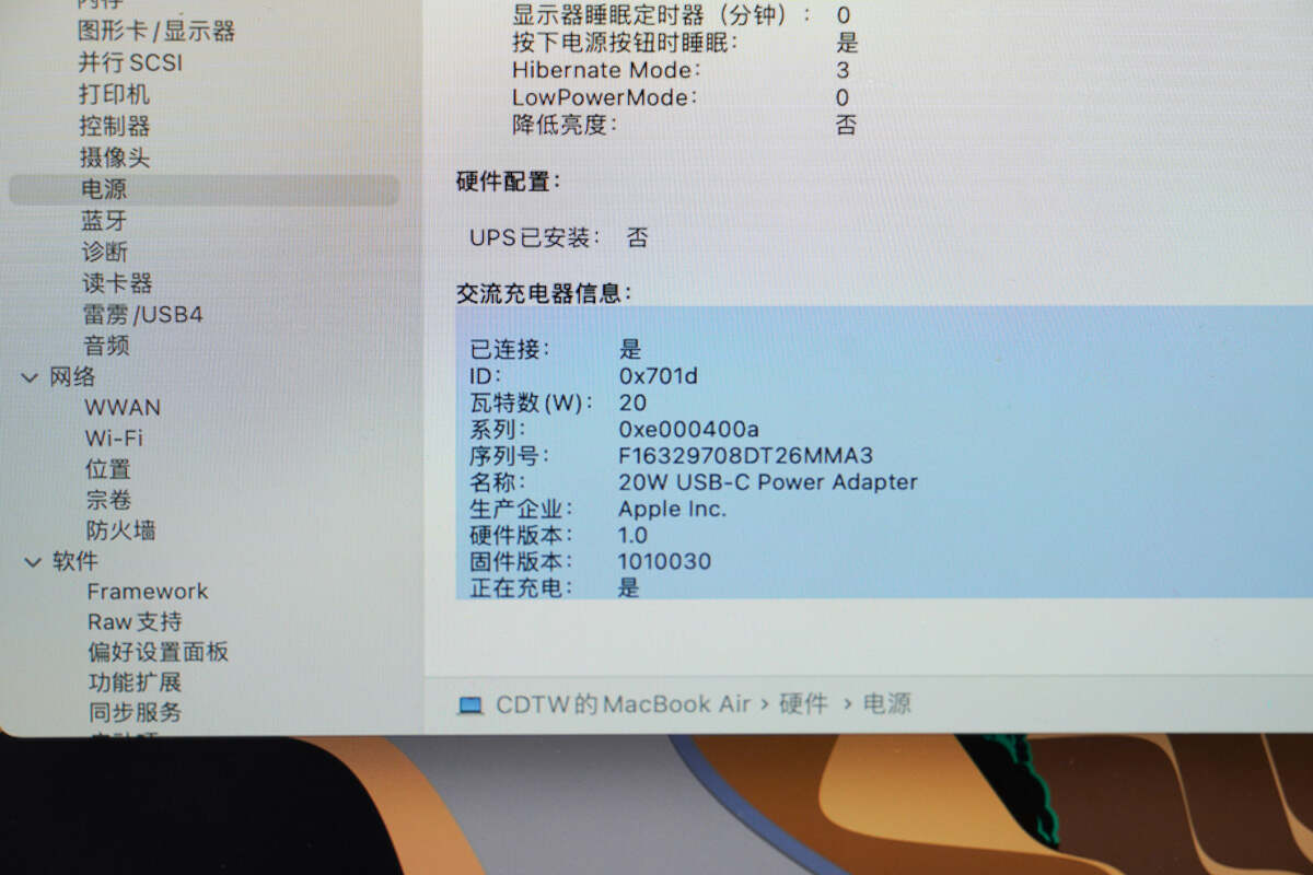
This serial number matches the one retrieved from the MacBook Air.
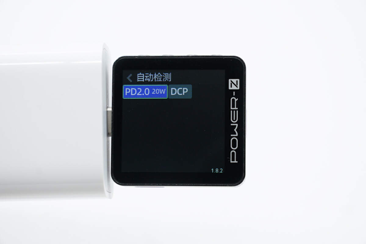
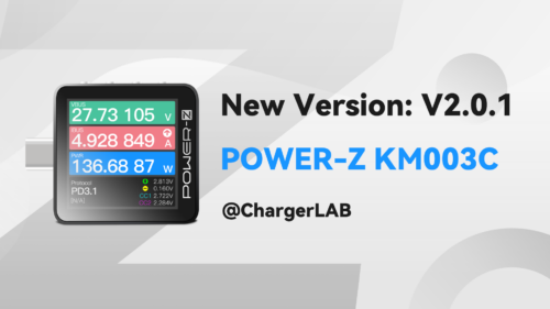
The ChargerLAB POWER-Z KM003C shows it only supports PD2.0 and DCP charging protocols.
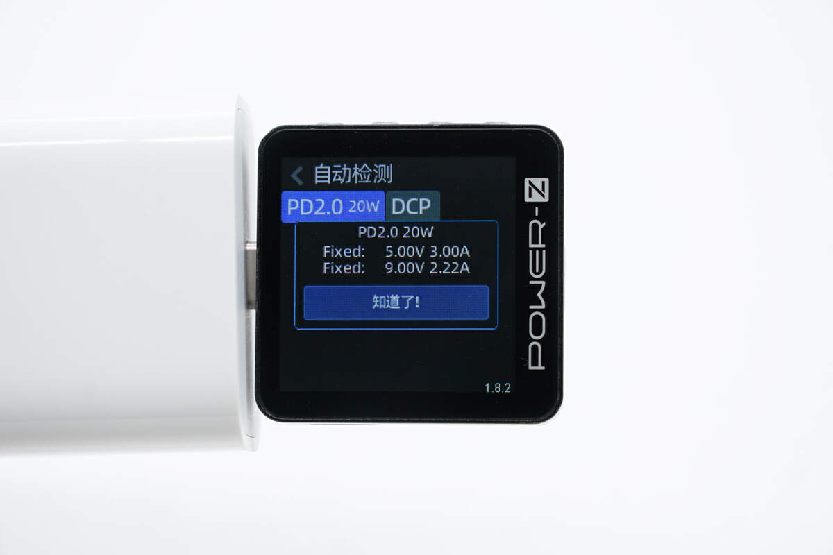
And it also supports two fixed PDOs of 5V3A and 9V2.22A.
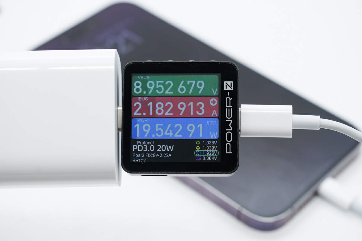
It can provide 8.95V 2.18A 19.54W of power to the iPhone 14 Pro Max.
Teardown
Now that we have completed our testing of this charger, it's time to take it apart and examine its internal components and structure.
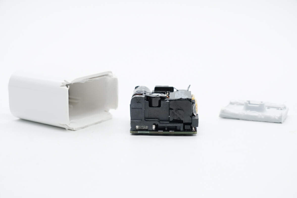
As always, let's try to cut it off using the cutting machine. The entire PCBA module can be easily pulled out.
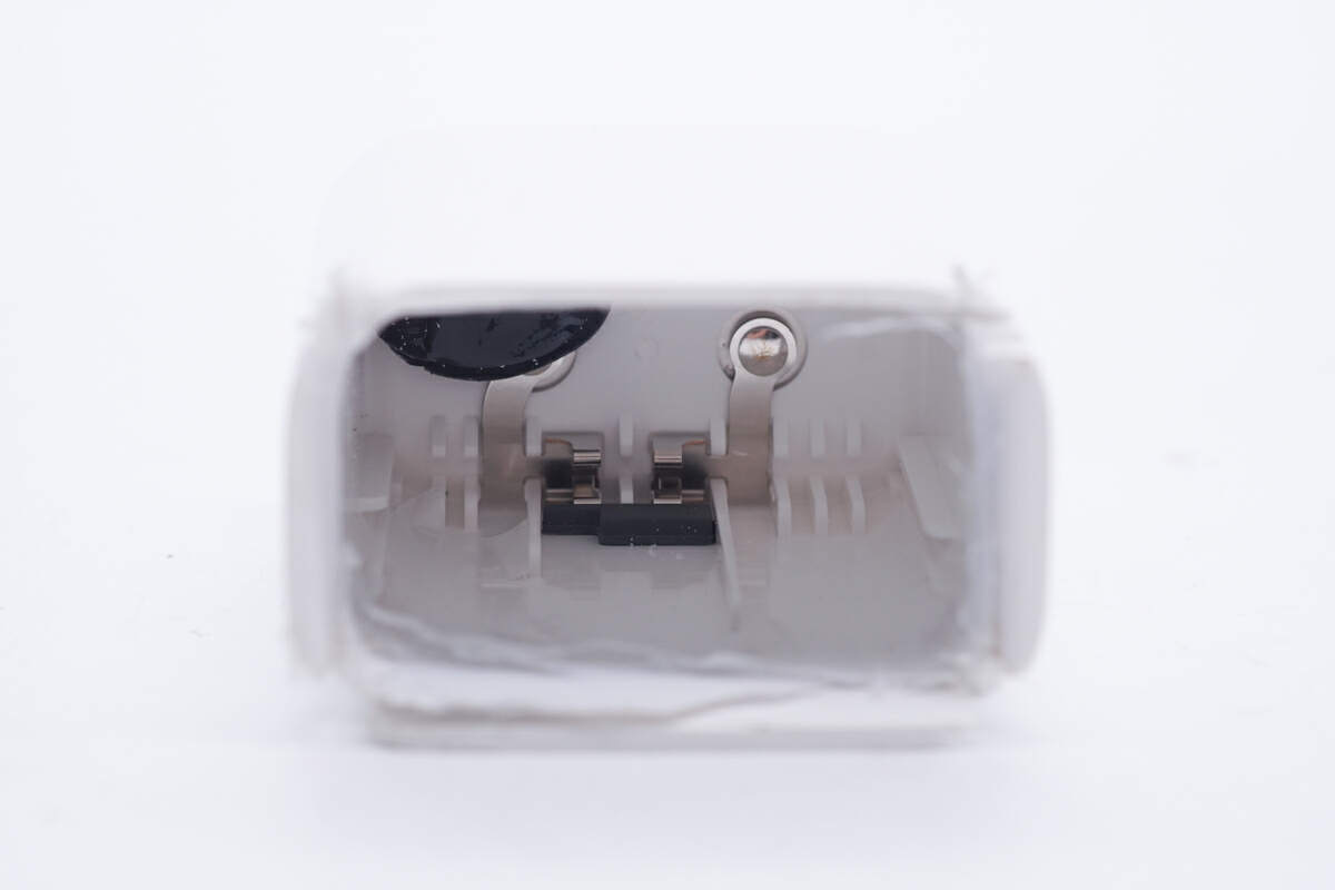
And the input prongs are connected to the charging module without wires.
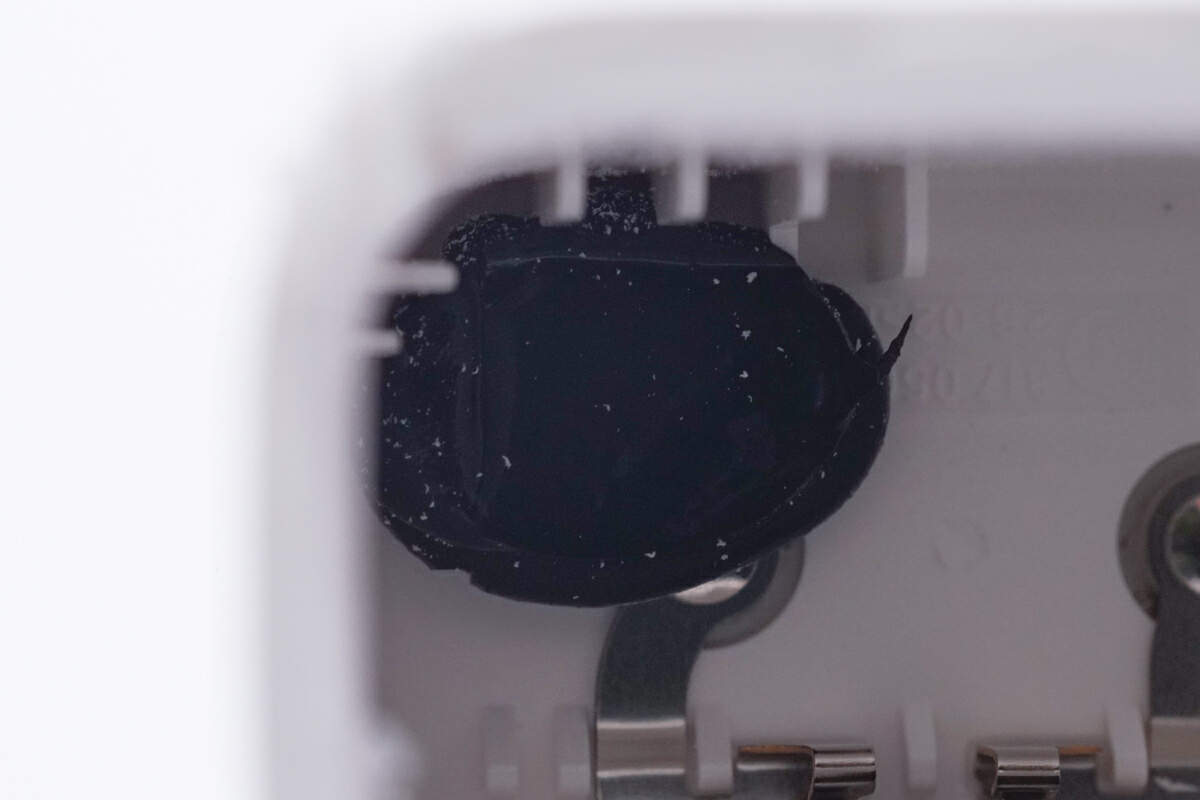
This black silicone block can dissipate heat from the transformer.
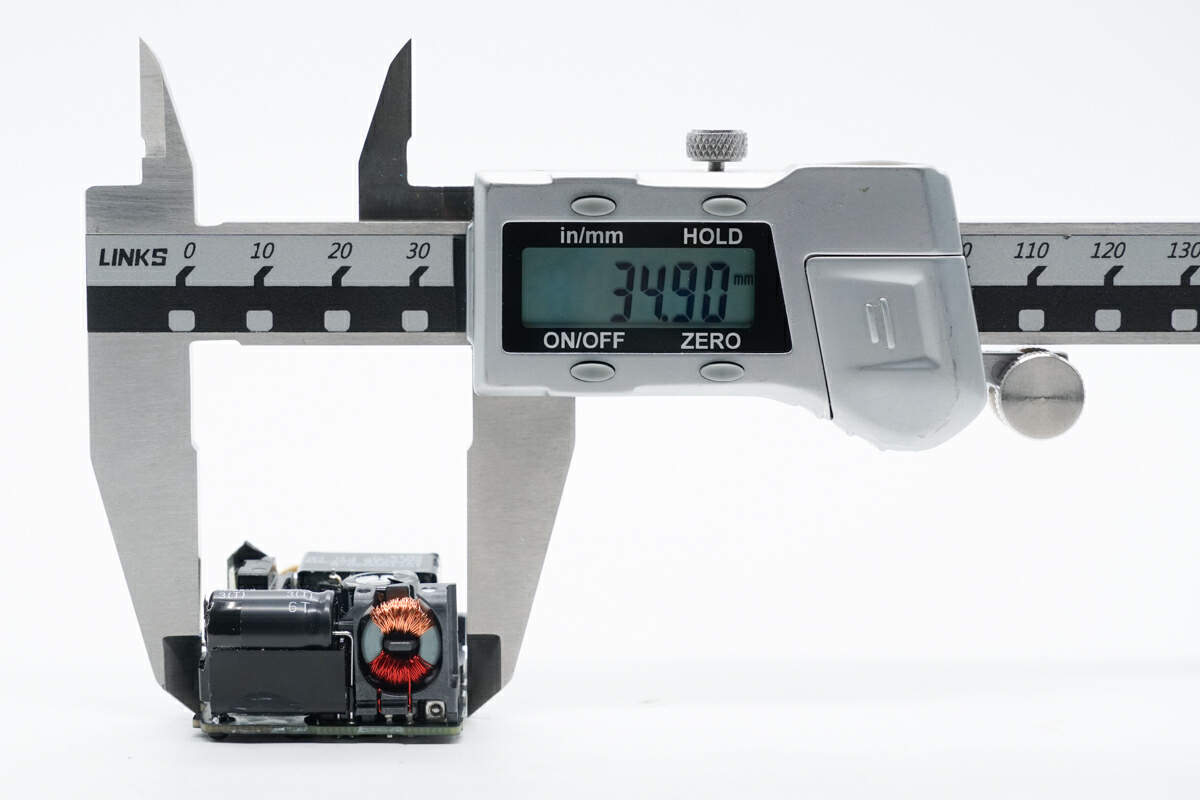
The length of the PCBA is about 35mm (1.38 inches).
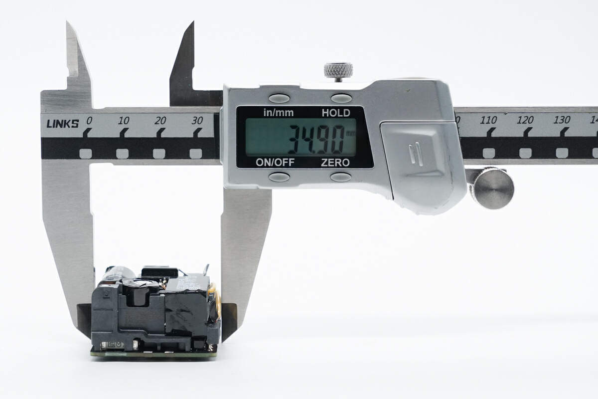
The width is also about 35mm (1.38 inches).
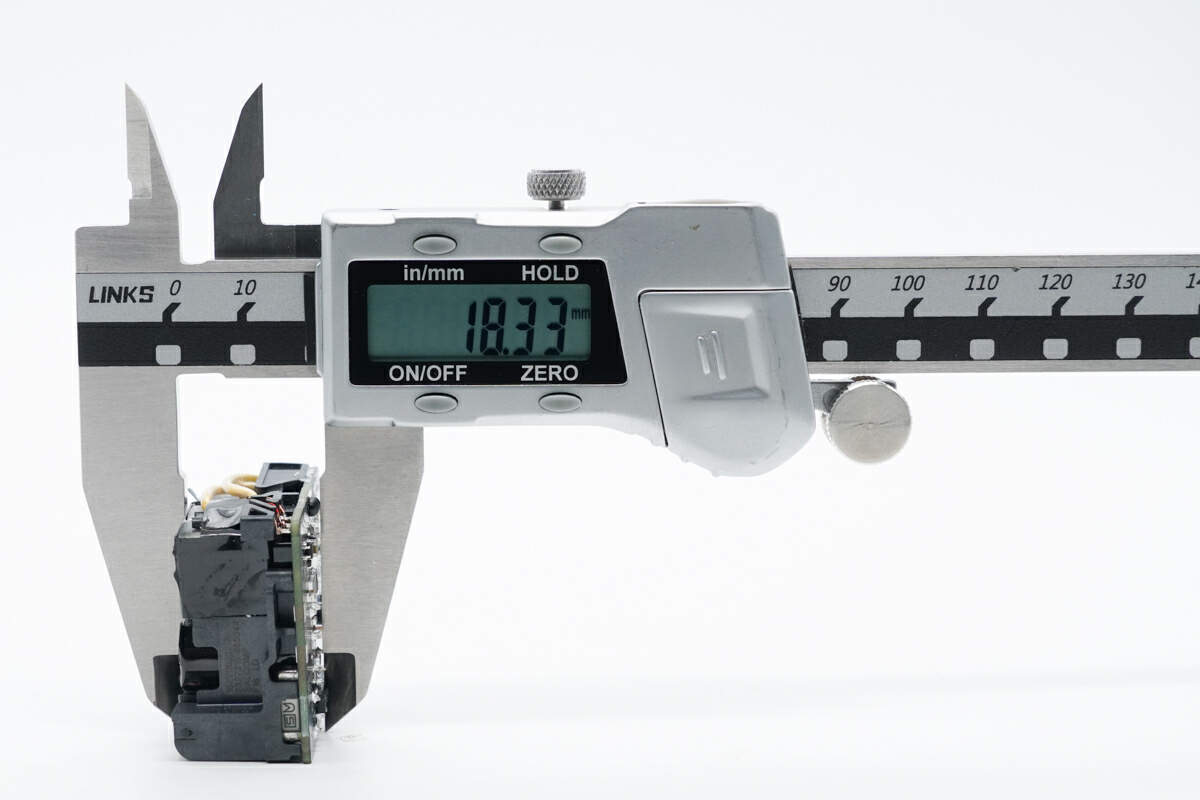
And the height is about 18mm (0.71 inches).
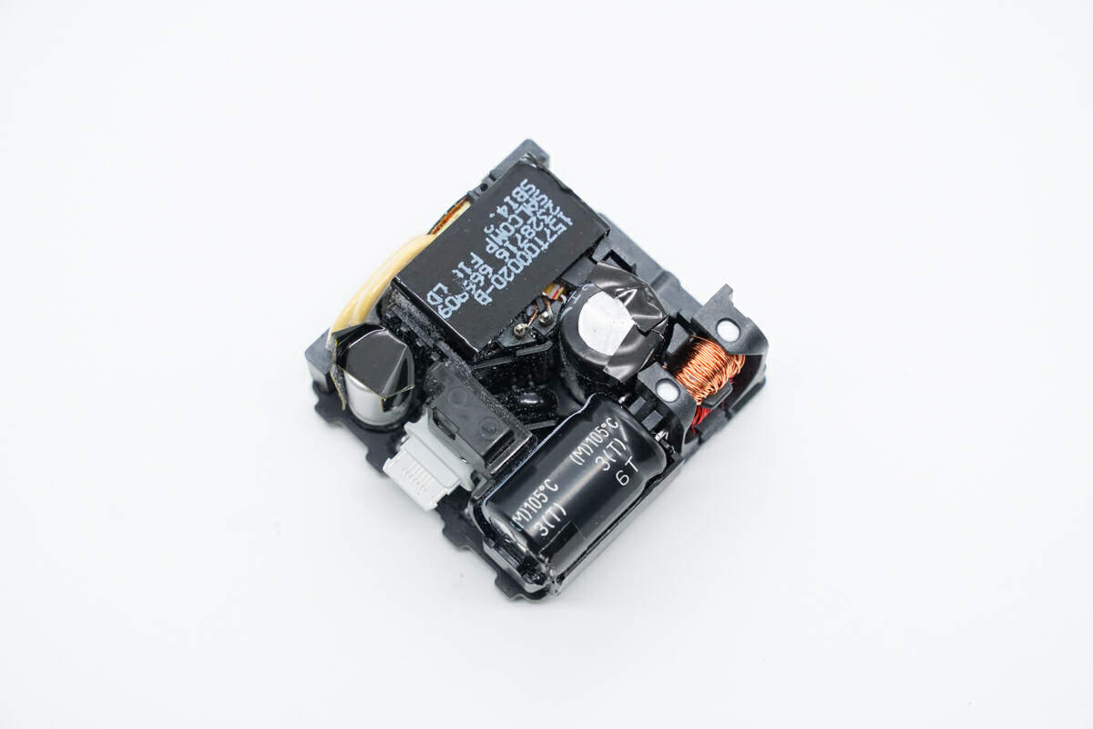
Almost all components on the front are black, but we still cannot find any GaN components. The common mode choke, capacitor, and other components are reinforced with plastic frames.
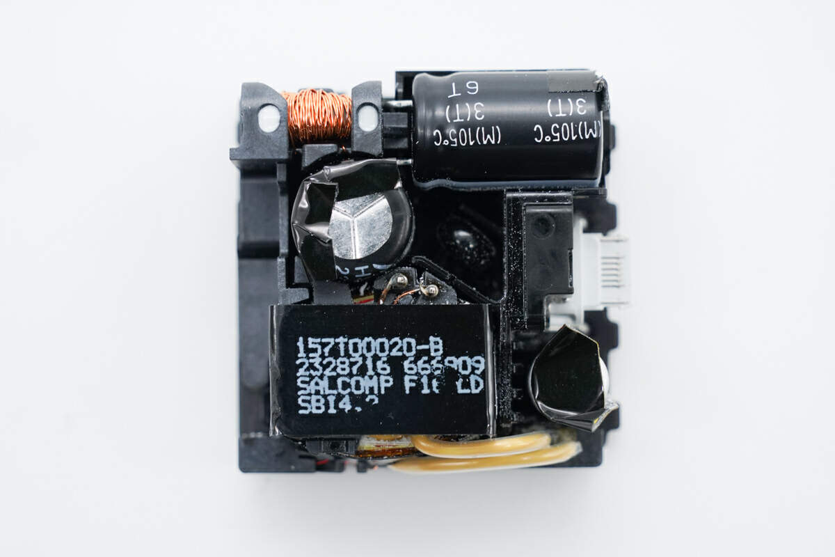
In the center, the high-voltage electrolytic capacitor and solid capacitor are affixed with black insulation tape.
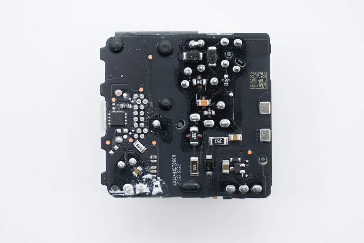
On the back, there's an output VBUS MOSFET, along with resistors, capacitors, and other small components. It's evident that the power supply solution used here offers a very high level of integration, resulting in a clean peripheral circuit.
ChargerLAB found this charger adopts switching power supply to output wide-range voltage, and then use the protocol chip of the secondary circuit to control the output voltage. Let's now dive into an understanding of various components, starting from the input side.
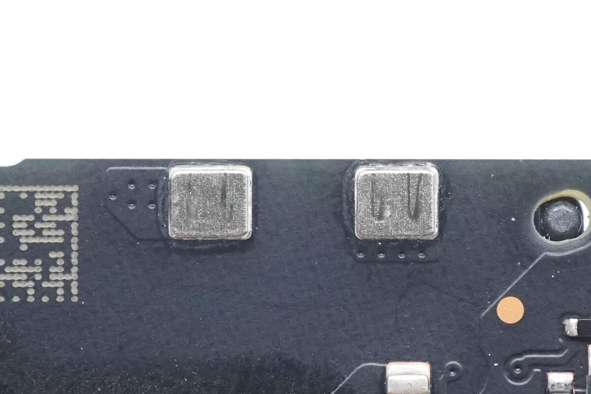
Here are the contacts of the input prongs,
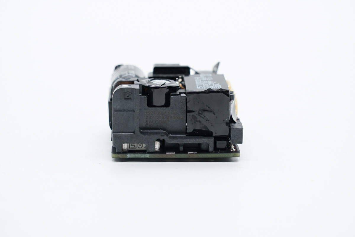
which are located under the plastic frame of the AC input end.
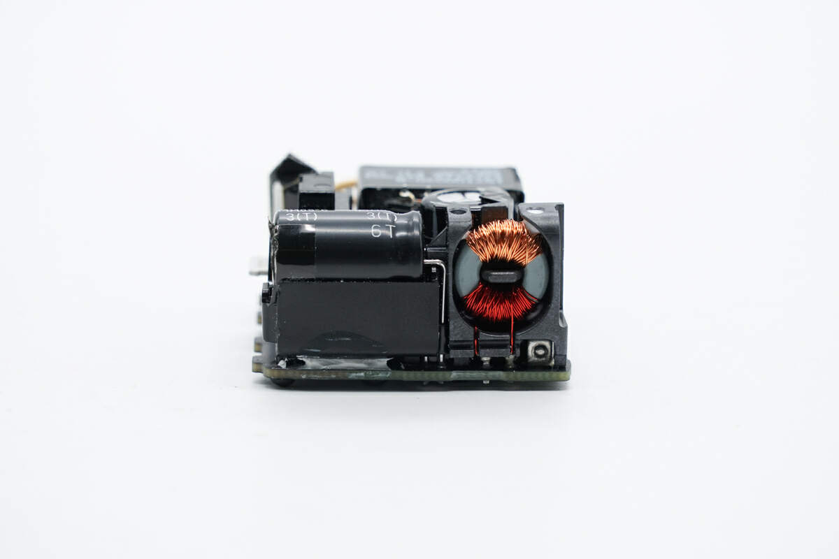
On one side of the module, there are common mode choke and high-voltage filter capacitor. The common mode choke is secured within a plastic frame, while the high-voltage filter capacitor is fixed on the outside of the plastic bracket.
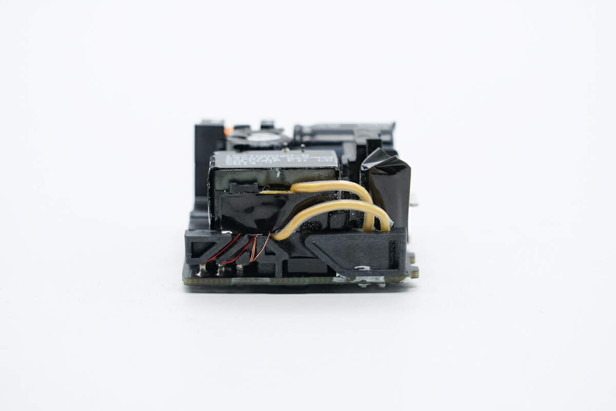
On the other side, there's a transformer, with the secondary winding made from multiple layers of insulated wire.
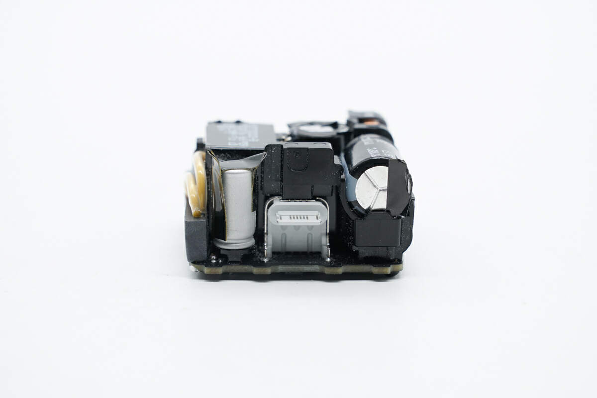
At the output end, the USB-C female socket is insulated using a plastic bracket.
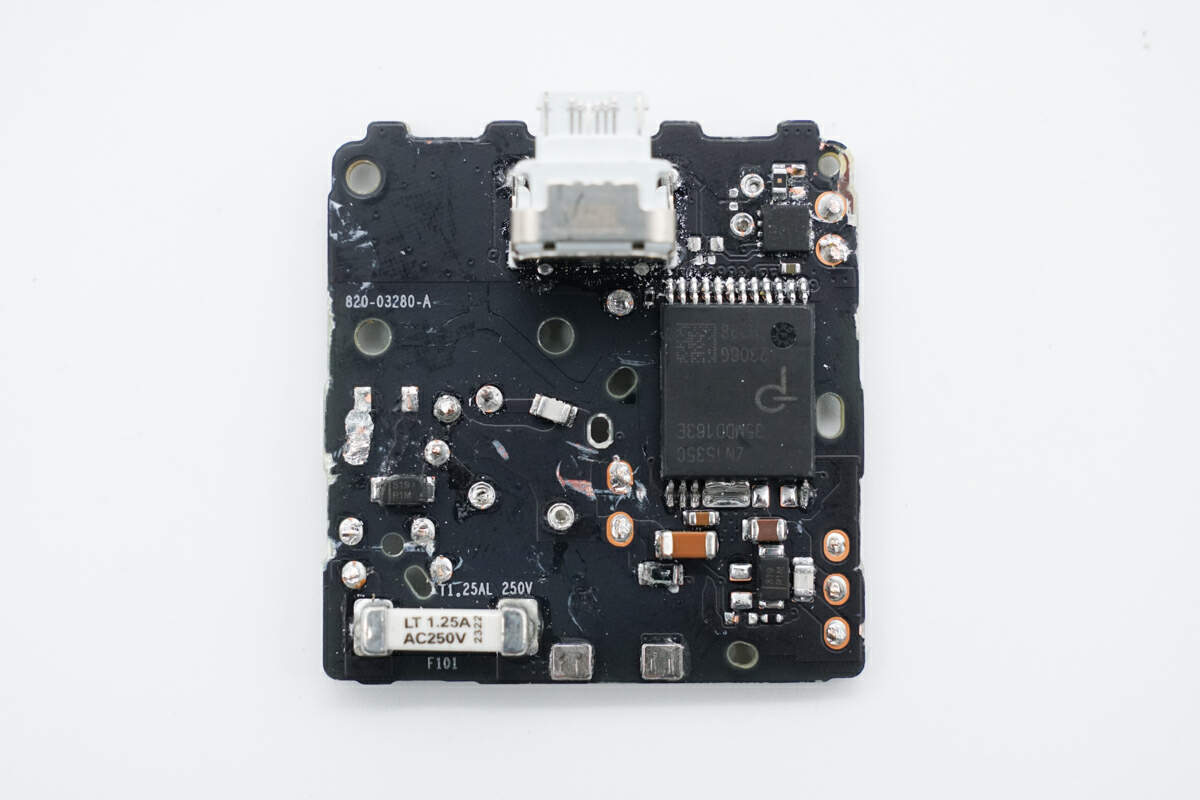
Removing the front components on the PCB reveals the presence of a fuse, rectifier diode, PI's master control chip, and synchronous rectification MOSFET.
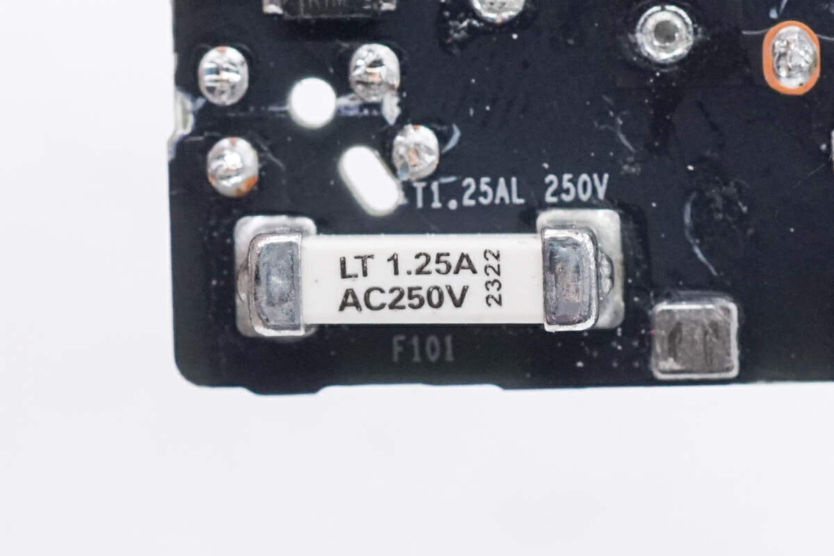
The input SMD fuse is from Littelfuse. 1.25A 250V.
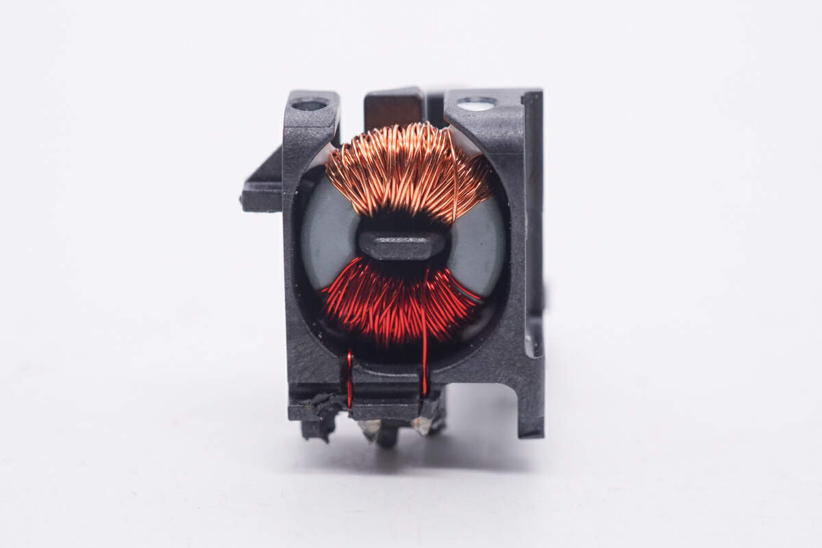
The common mode choke is wound with red and copper wires and fixed inside the plastic frame.
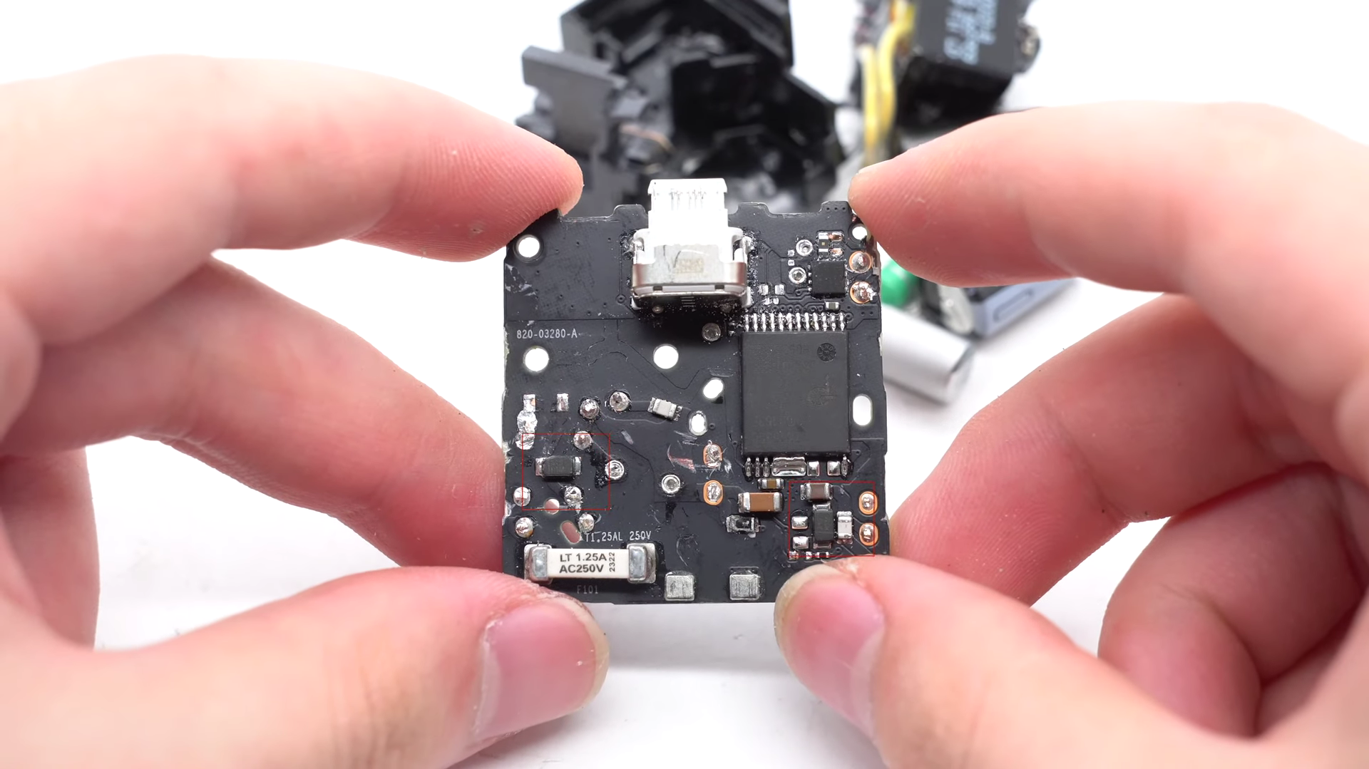
Those four diodes on the front,
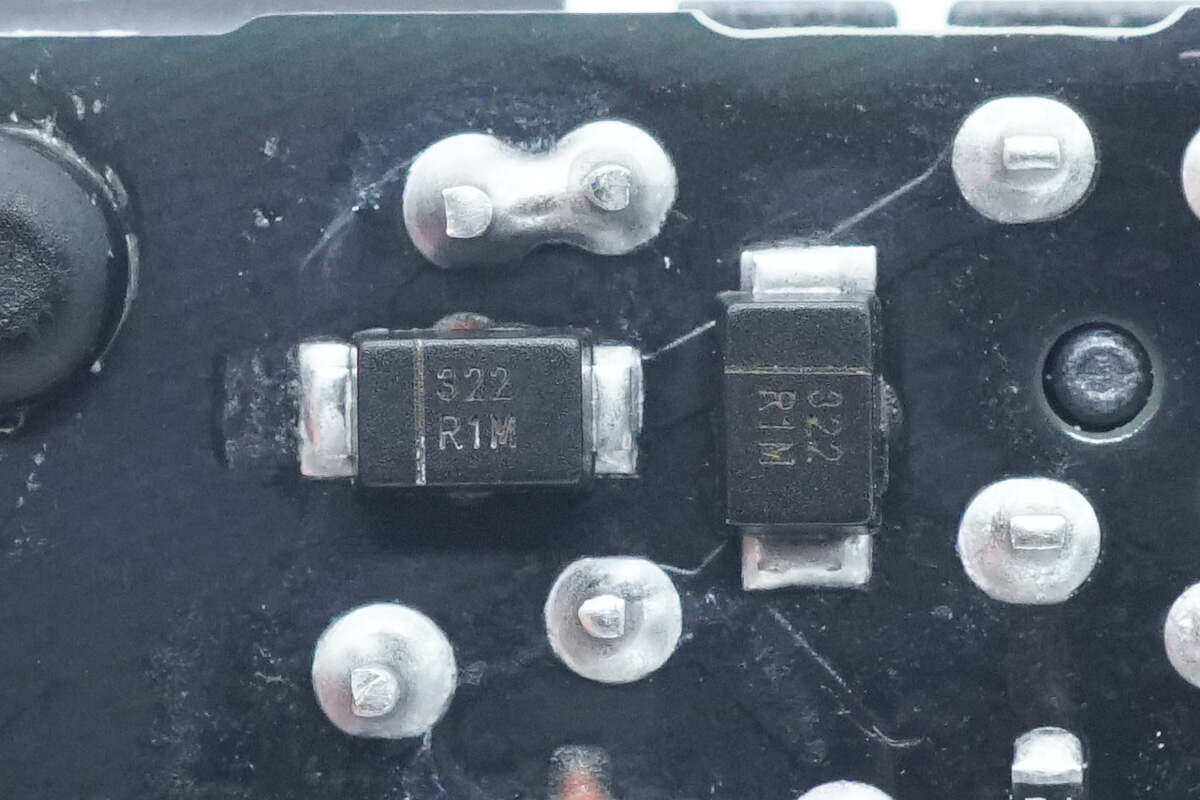
and back can form a bridge rectifier. They are marked with R1M and can be used to rectify AC into pulsed DC.
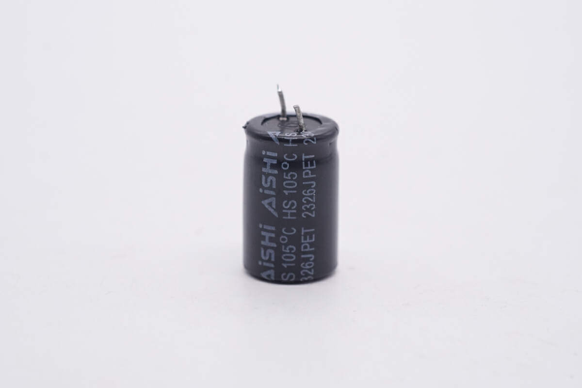
One of the electrolytic capacitors is pasted with insulating tape and is from AiSHi. 400V 15μF.
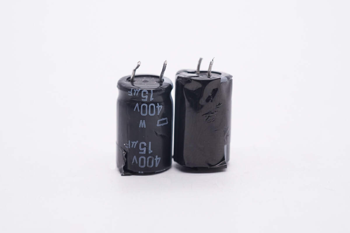
There are two electrolytic capacitors in total. The other one is from Chemi-Con. 400V 15μF.
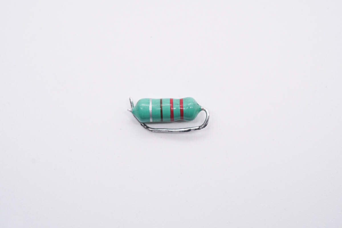
The differential mode choke is a color ring inductor.
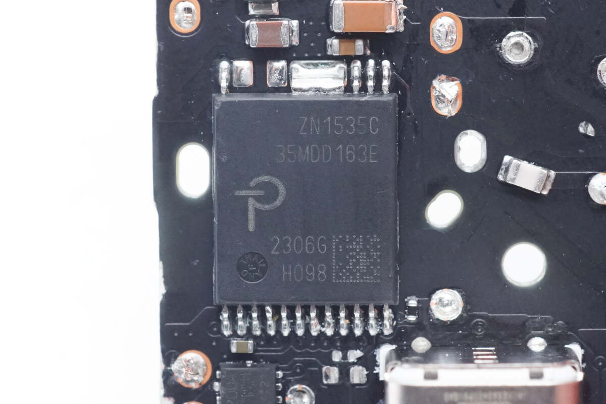
Then, this is the protagonist and largest chip of this charger. It's actually a customized master control chip from PI, marked with ZN1535C. There's no protocol chip inside this charger, cause it has been integrated into this chip. Except for that, it also integrates MOSFET, PWM controller, synchronous rectification controller, magnetic coupling, etc. So, we can call it "Power IC".
This design greatly simplifies the design and manufacturing of flyback power converters, especially for those that require high efficiency or compact size. It also enhances system reliability and stability.
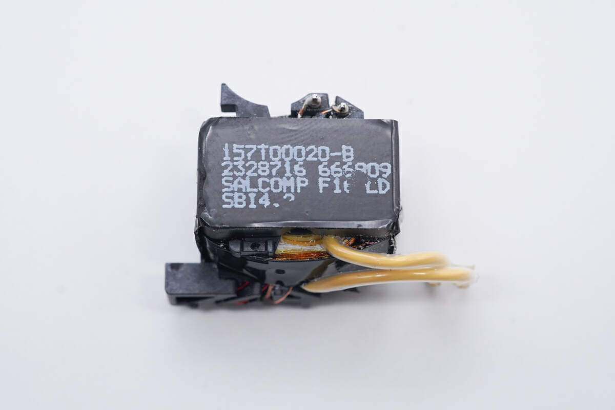
Here is the transformer, manufactured by Salcomp.
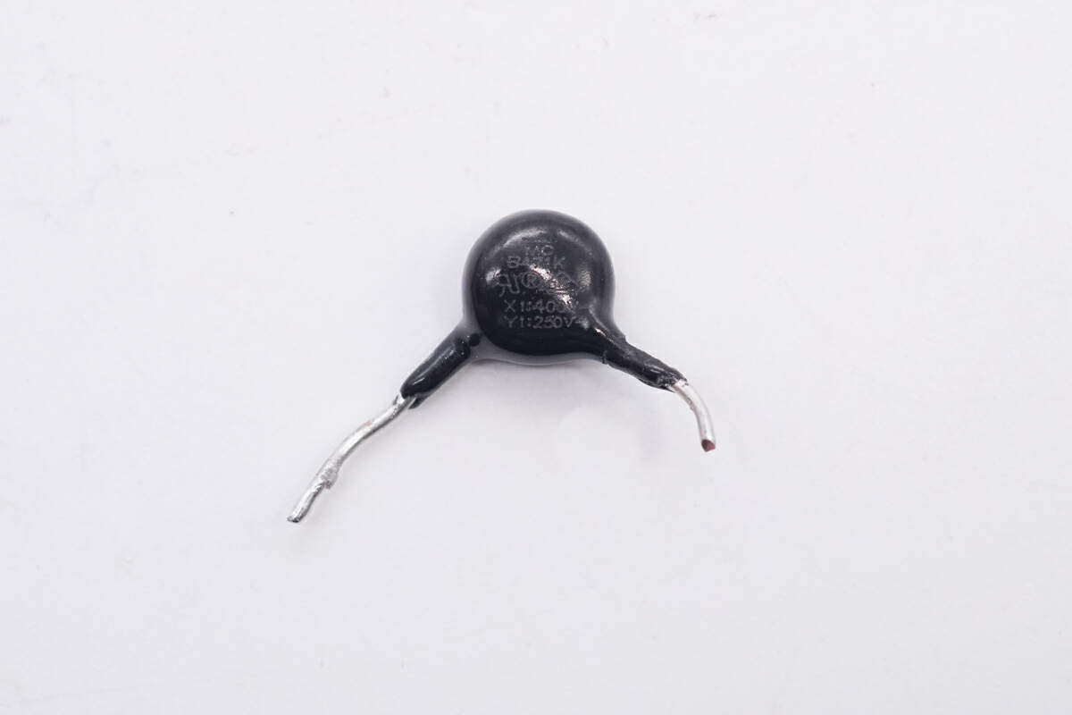
And here is the black Y capacitor.
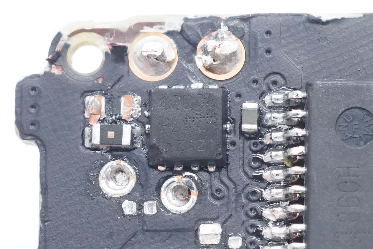
The synchronous rectifier is from Toshiba. 100V, 9.8mΩ. Model is TPN1200APL.
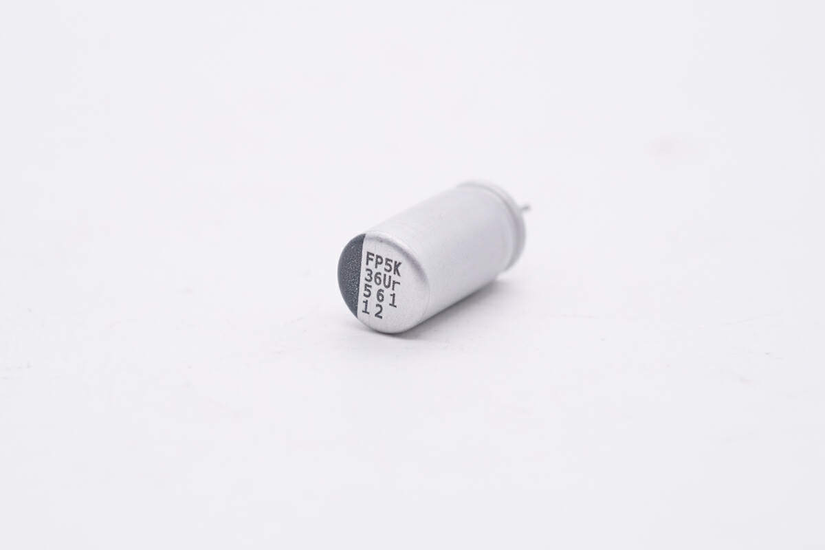
The solid capacitor for output filtering is from nichicon. 12V 560μF.
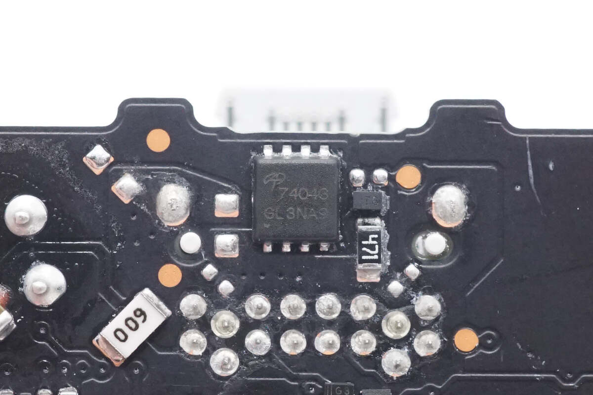
The output VBUS MOSFET is from AOS and adopts DFN3 x 3 package. 20V, 4.4mΩ. Model is AON7404G.
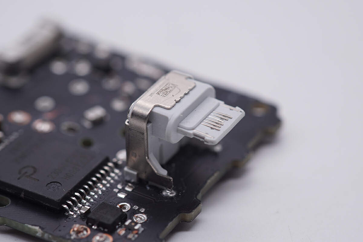
Finally, the USB-C female socket is reinforced with a metal plate and fixed with plastic frame.
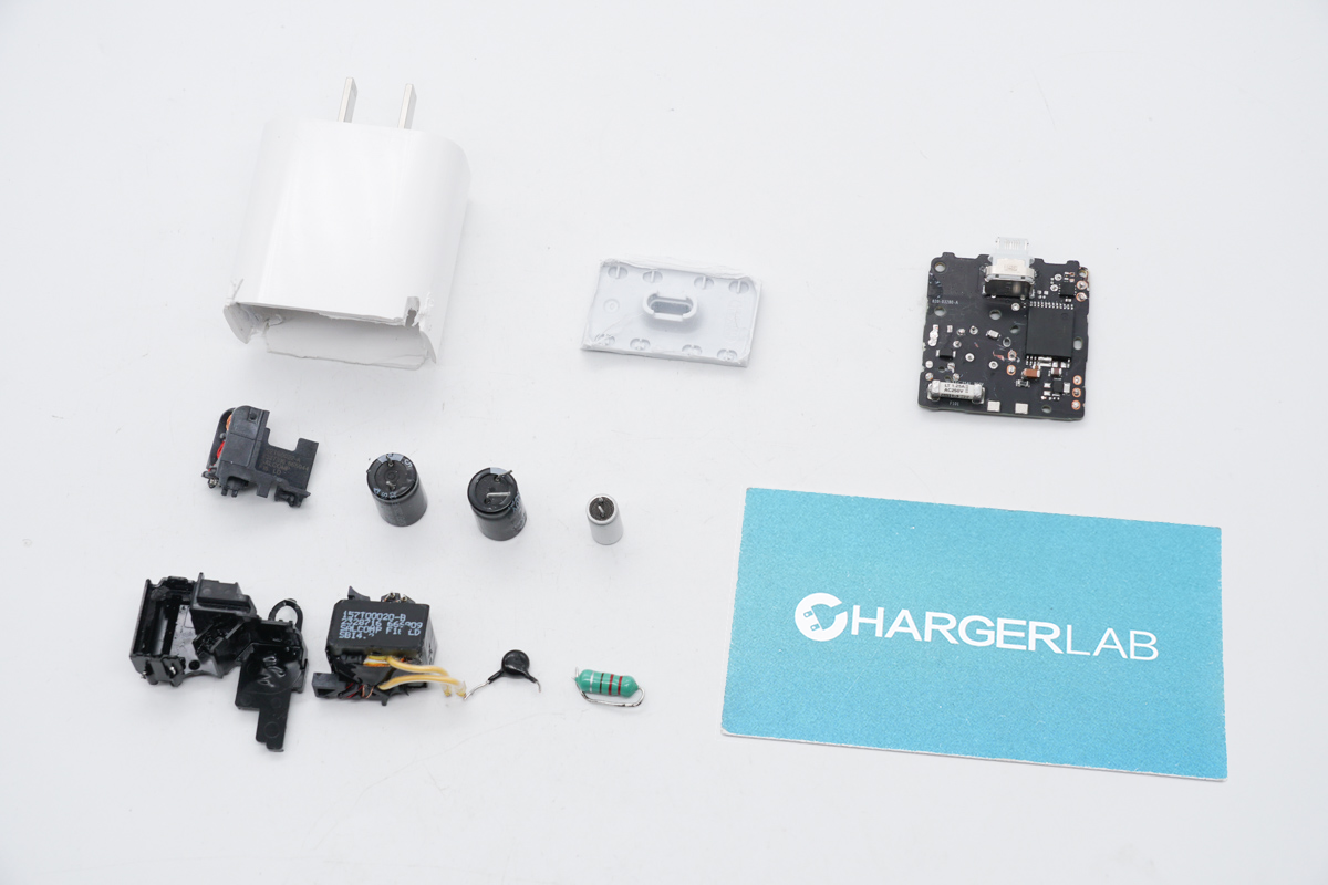
Well, that would be all components of new Apple 20W charger.
Summary of ChargerLAB
The new Apple 20W charger retains its classic appearance, with no changes in overall size. It has been tested to support PD 2.0 fast charging, featuring two fixed PDOs of 5V3A and 9V2.22A. In terms of both appearance and performance, it remains consistent with the original version, providing a familiar user experience.
ChargerLAB's teardown reveals that the charger's internal design follows the classic Apple style. The PCBA module is predominantly black, and common mode chokes, capacitors, and other components are supported and fixed with plastic frames. The charger utilizes a switching power supply solution with custom components from renowned manufacturer PI, achieving a new level of integration. Considering the current popularity of GaN IC technology and the introduction of Southchip's POWERQUARK series of fully integrated chips, this offers a glimpse into the industry's development trends. The charger is manufactured by Salcomp, known for its excellent craftsmanship and materials.
With GaN components, perhaps one day, Apple can achieve 20W output power in the volume of a 5W charger.
Related Articles:
1. What's Difference Between Apple 20W and Apple 18W Charger
2. Teardown of Apple 20W Power Adapter (For iPhone 14 Series)
3. Updated Power IC | Teardown of New Apple 20W Charger (Video)

