Introduction
The introduction of GaN technology has significantly reduced the size of chargers, making them easier to carry. However, conventional chargers still have a square design and are relatively thick, making them inconvenient to carry. Recognizing this pain point, several brands have focused on it and introduced ultra-slim GaN chargers in various cookie-like shapes to meet the personalized needs of consumers.
Recently, we got a brand-new ultra-slim charger from Baseus. It can support up to 65W output power, but the thickness is only about 16.6mm or 0.66 inches.
It's also equipped with a USB-A and a USB-C port for fast charging. Let's go ahead and take it apart to see how it can be so thin.
Product Appearance
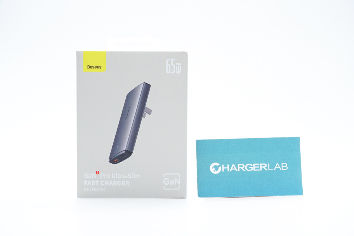
The packaging continues to adopt Baseus' design with the maximum output power of 65W printed on the top right corner.
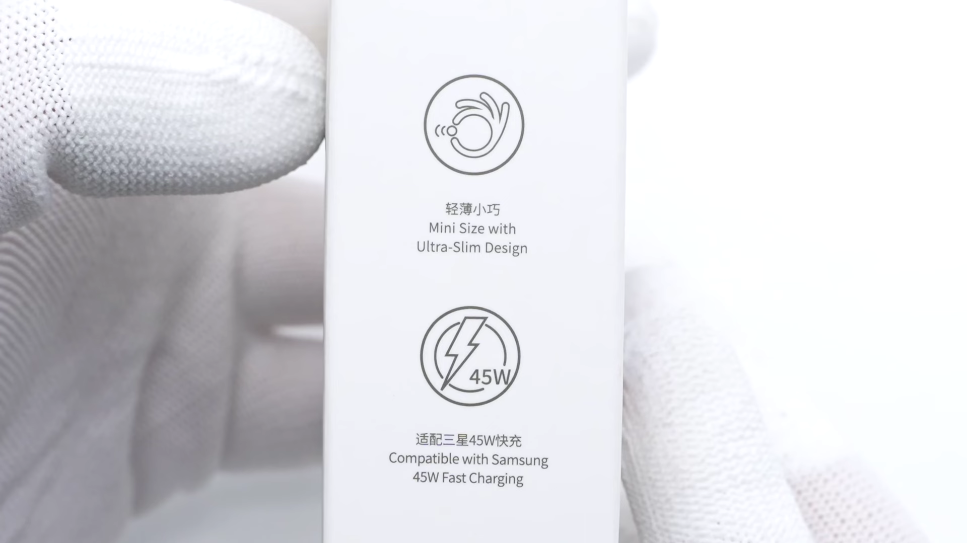
Except for its ultra-slim design, it's also compatible with Samsung 45W Fast Charging.
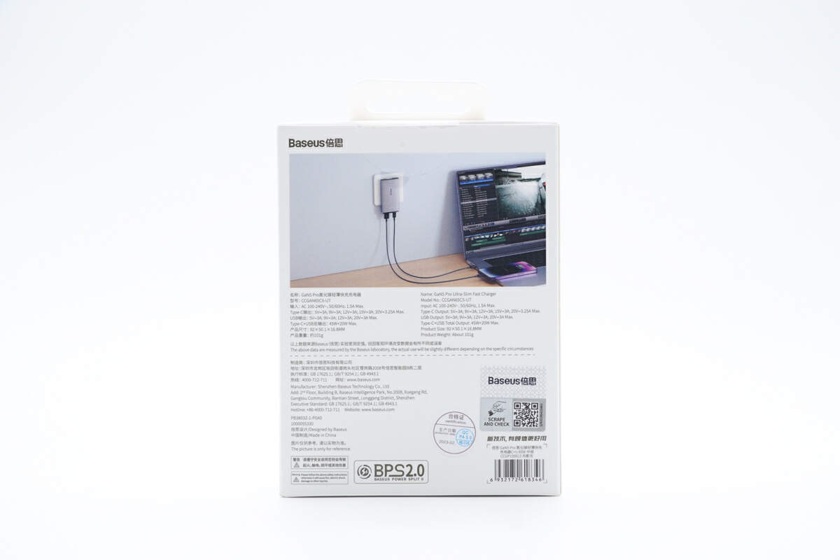
All specs info are printed on the back. We'll talk about it later.
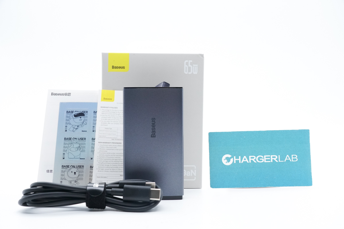
It contains the charger, cable, manual, and some stickers.
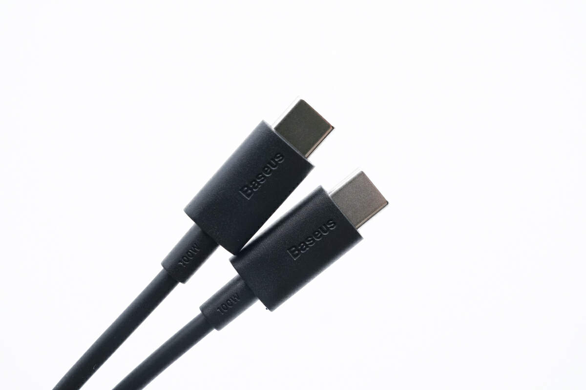
The Baseus logo and the 100W are engraved on the matte USB-C connector.
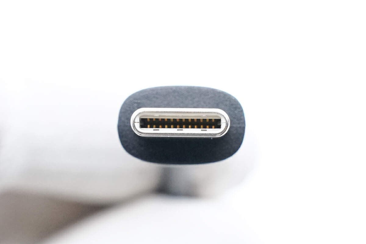
And it adopts a full pin design.
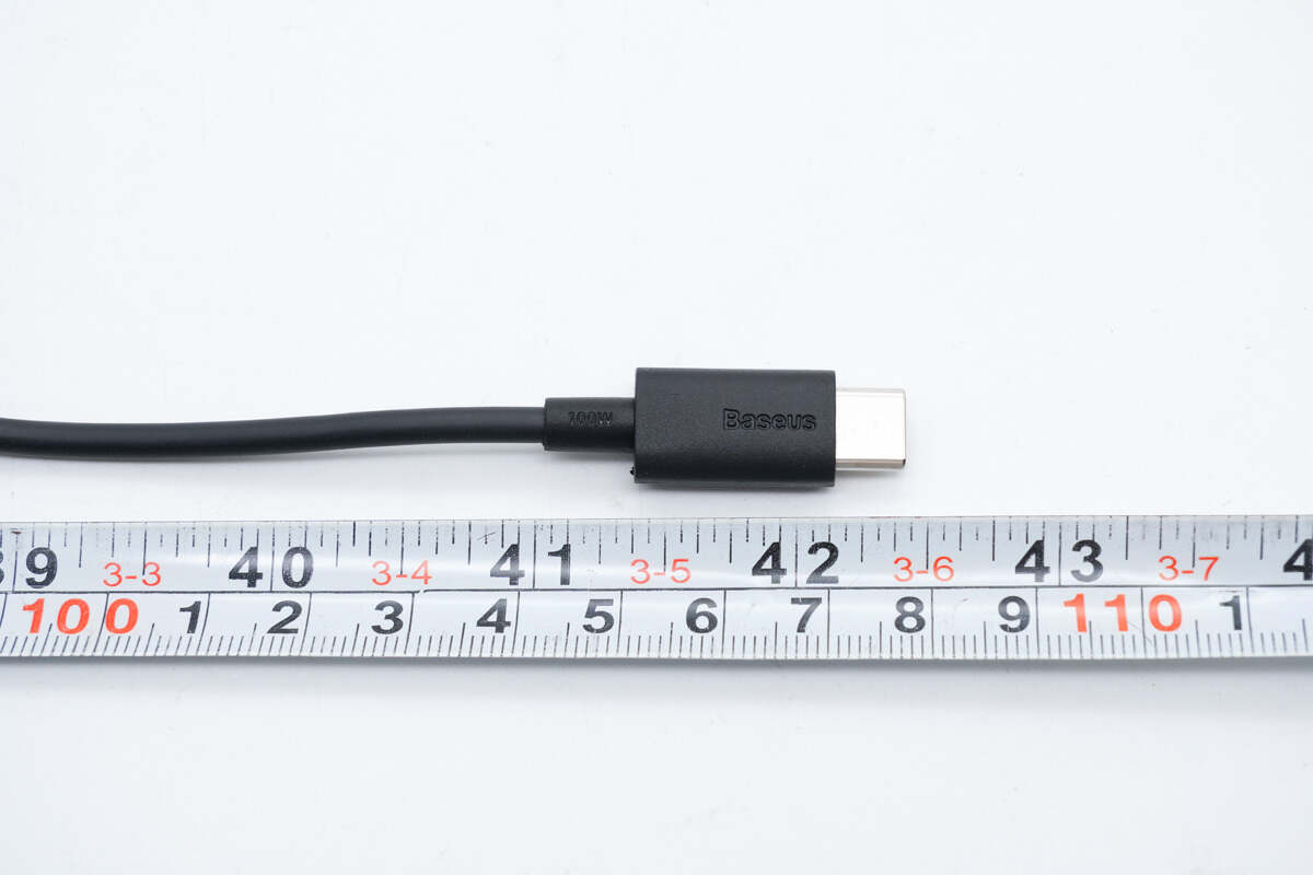
This cable is slightly longer than 1m (3' 3.37'').
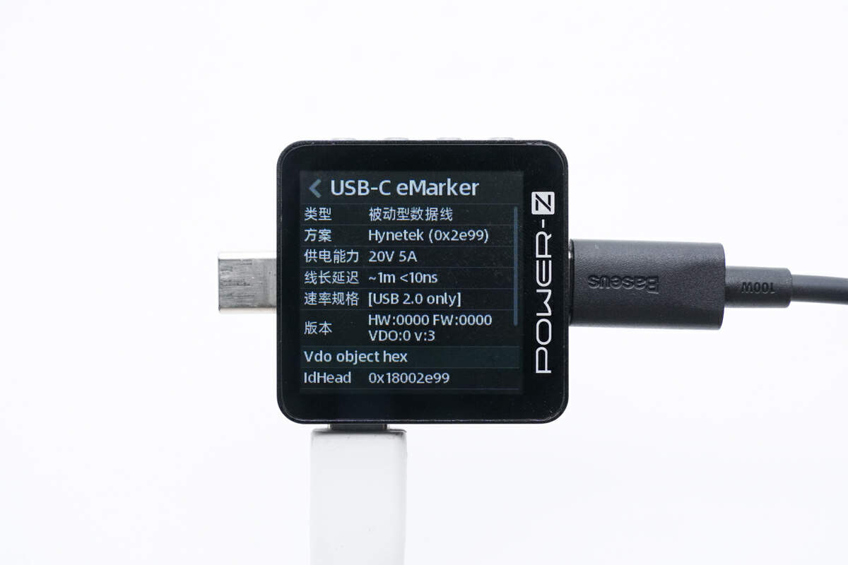
The ChargerLAB POWER-Z KM003C shows it integrates an E-Marker chip and can support 100W, but it only supports USB 2.0.
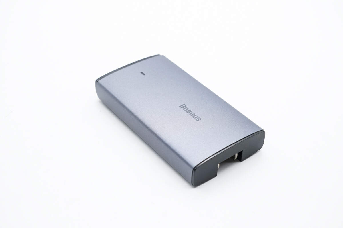
The charger is equipped with a fire-retardant outer casing treated with metallic paint coating. The outer case has a matte finish, giving it a smooth texture.

The baseus logo is printed on the front.

And the indicator light below it can show the charging status.
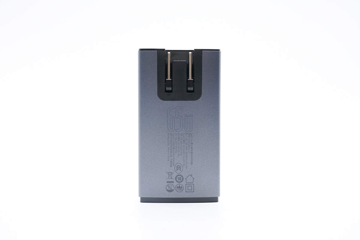
Flip to the back.
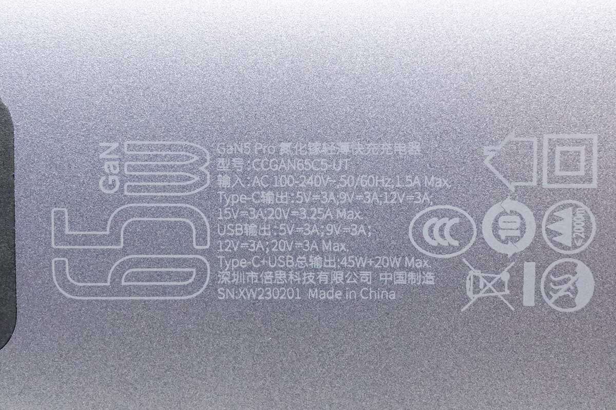
Model is CCGAN65C5-UT. It supports input of 100-240V~50/60Hz 1.5A. The USB-C can provide up to 65W output power, while the USB-A only supports up to 60W. When charging two devices, the power will be divided into 45W and 20W.
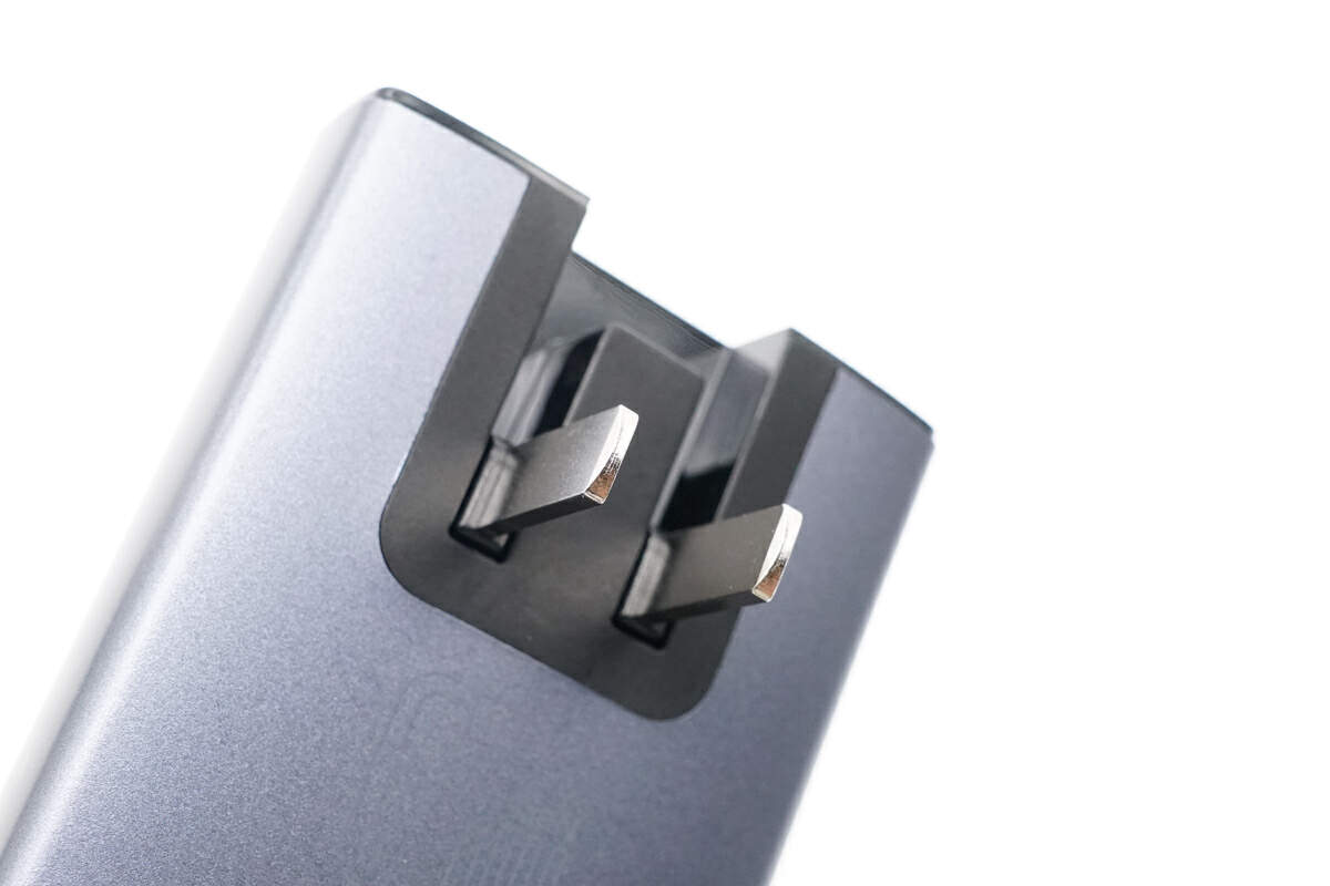
The input prongs can be folded, which is quite reasonable for an ultra-slim charger
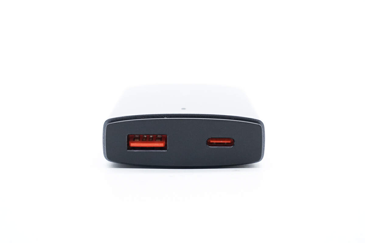
And both output ports are orange.
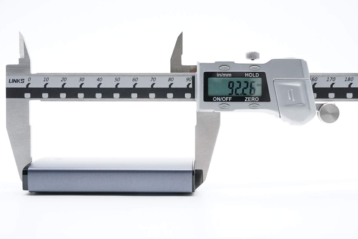
The length of this charger is about 92mm (3.62 inches).
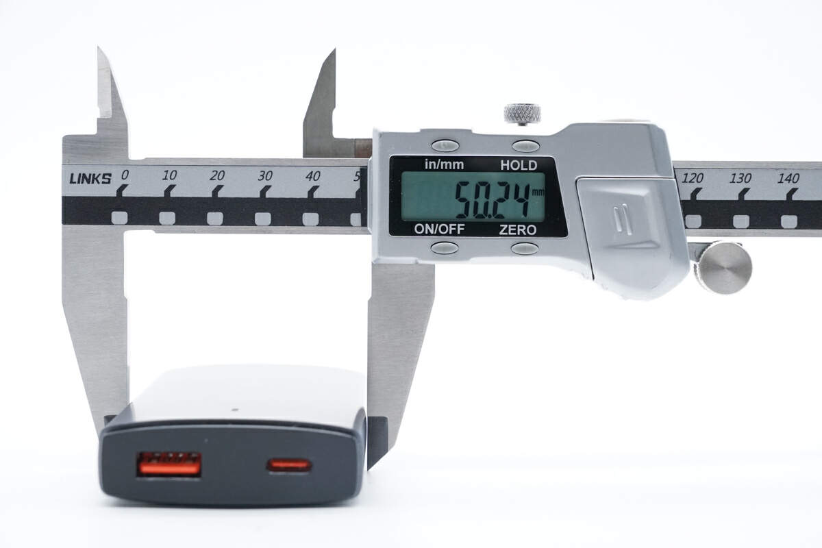
The width is about 50mm (1.97 inches).
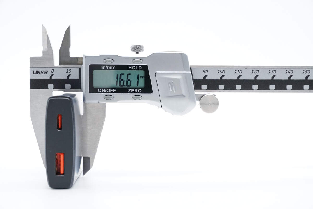
The height is about 16mm (0.66 inches)
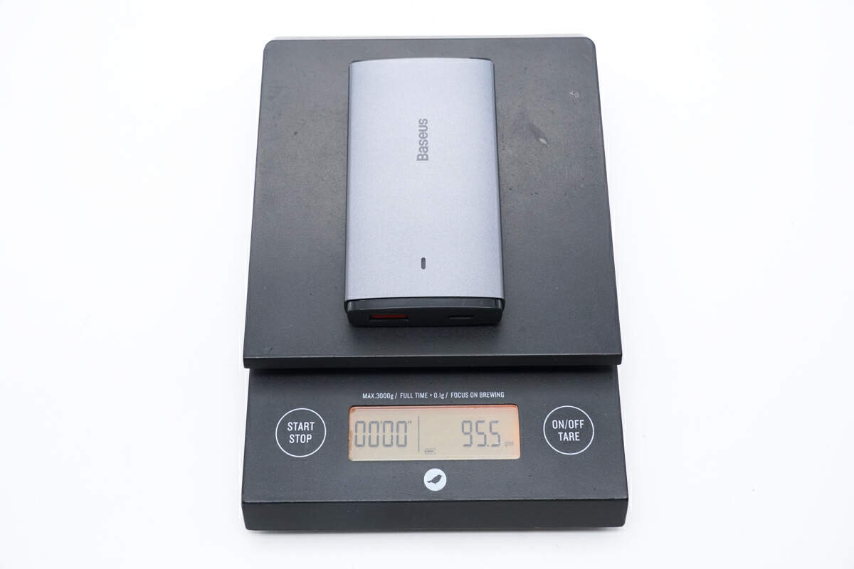
And the weight is about 95.5g (3.37 oz).
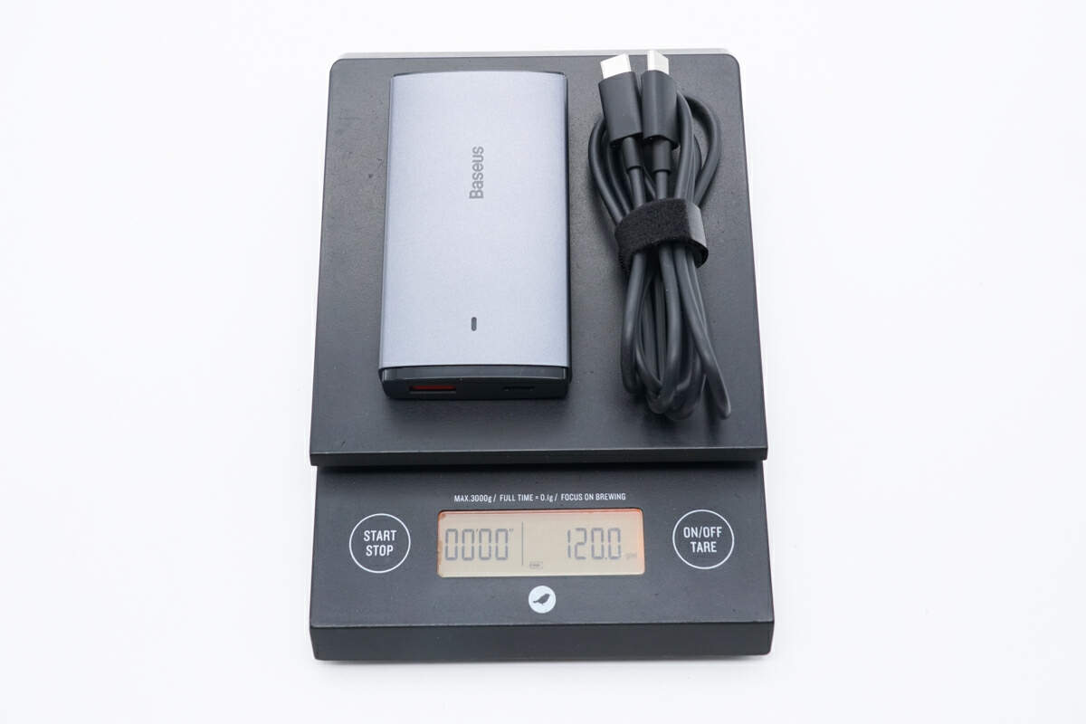
The total weight is 120g (4.23 oz).
After connecting to the power supply, the light on the front will light up.
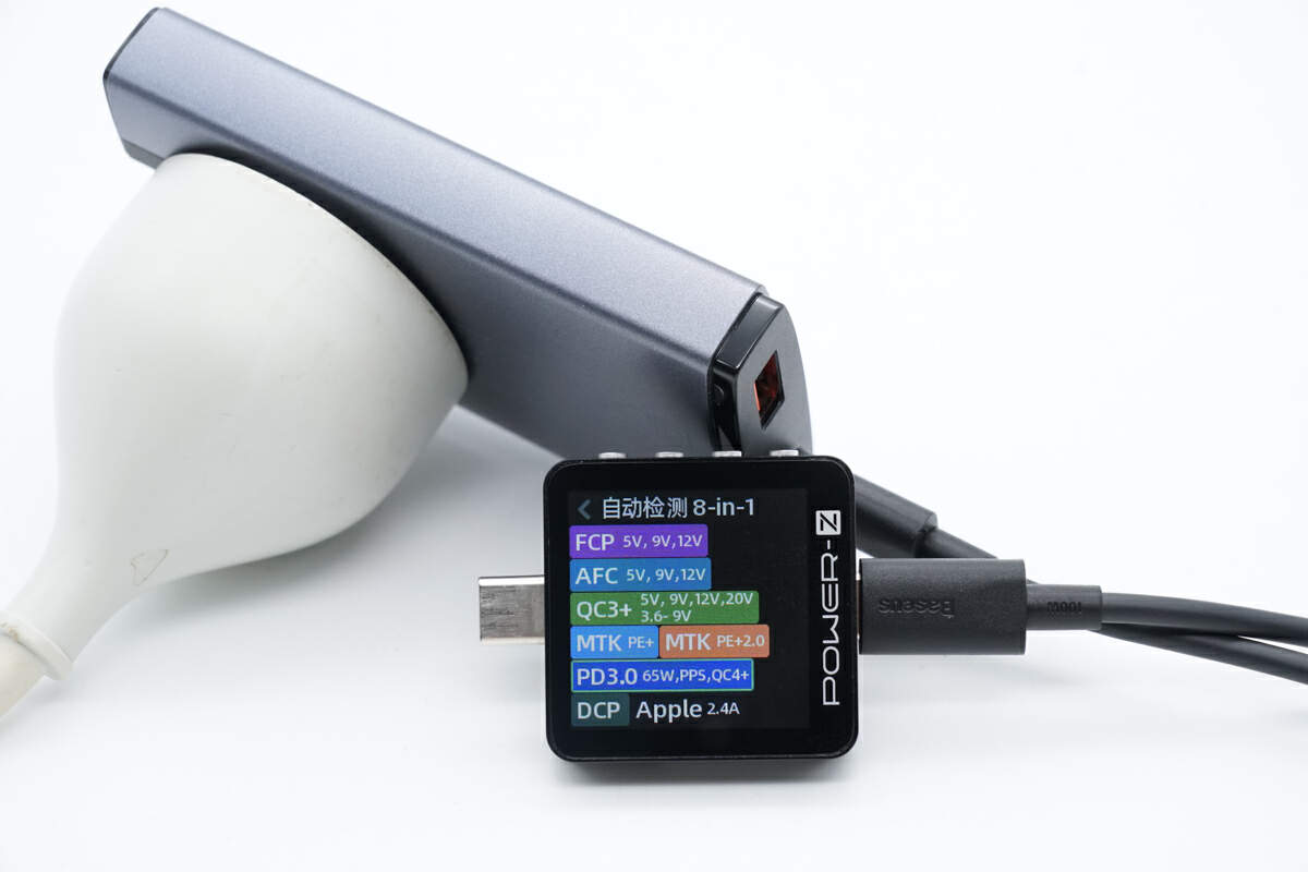
The ChargerLAB POWER-Z KM003C shows the USB-C supports FCP, AFC, QC3+/4+, PD3.0, PPS, DCP, and Apple 2.4A protocols.
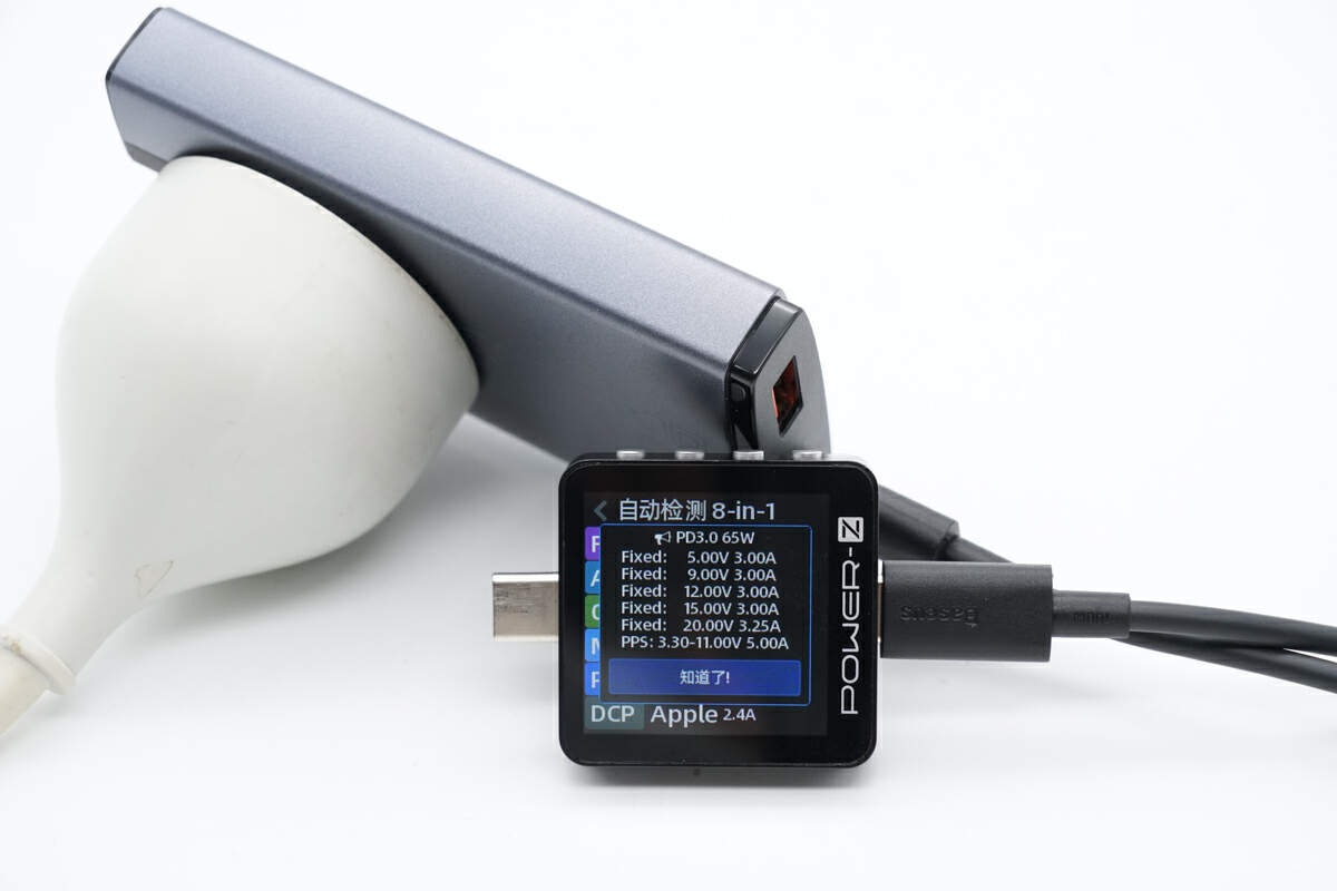
It also has five fixed PDOs of 5V/9V/12V/15V 3A, 20V 3.25A, and a set of PPS.

The USB-A port supports FCP, SCP, AFC, QC3.0, DCP, and Apple 2.4A protocols.
Teardown
Now that we have completed our unboxing and testing of this charger, it's time to take apart the device and examine its internal components and structure.

Next, let's use the spudger to pry along the gap of the input end.
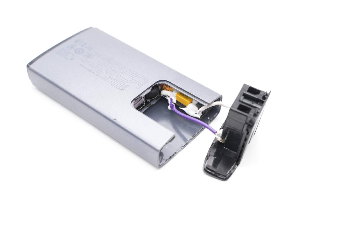
The input module is inserted here and is connected to the input wires through white and purple wires.
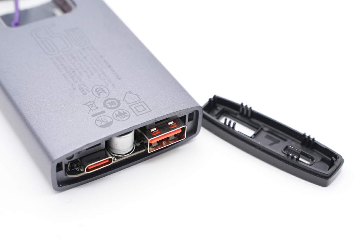
Next, remove the small cover on the output end.

But we cannot take it out and have to get help from "cutting machine."
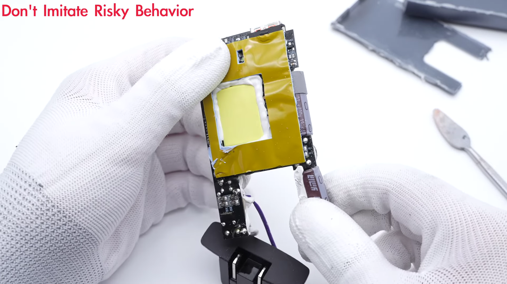
Finally, we can see the entire PCBA module.

And disconnect the input module from the main PCB.
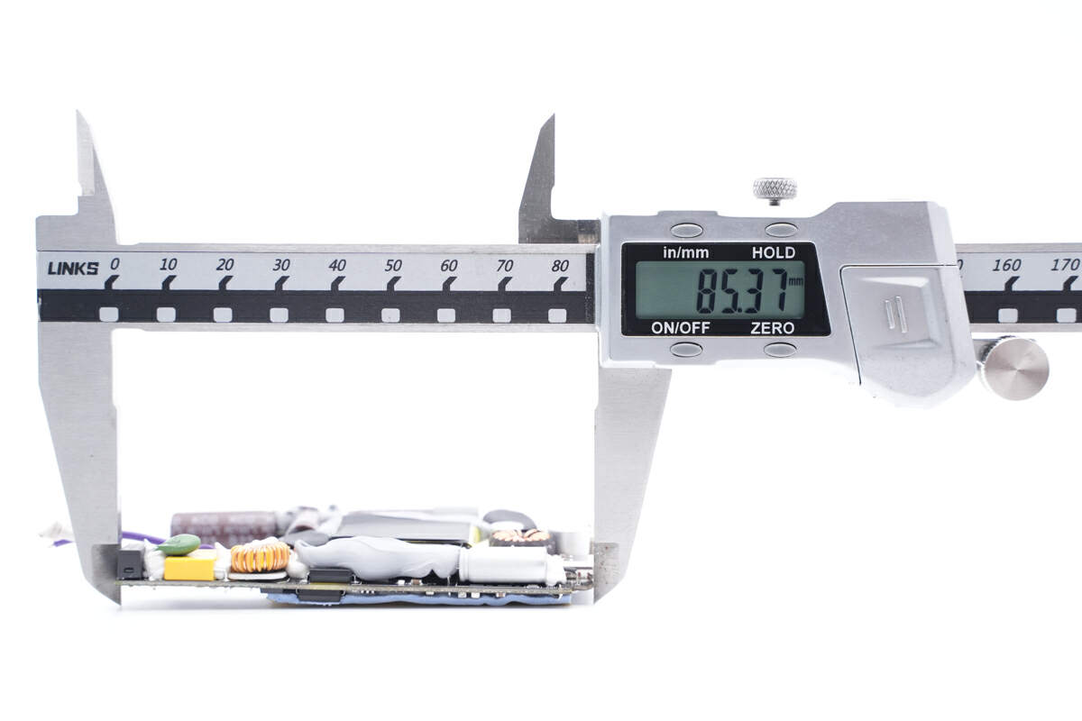
The length of the PCBA is about 85mm (3.35 inches).
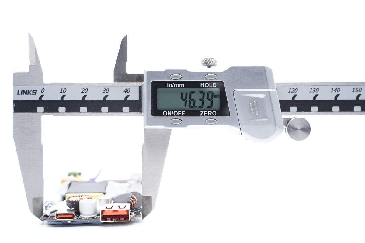
The width is about 46mm (1.81 inches).
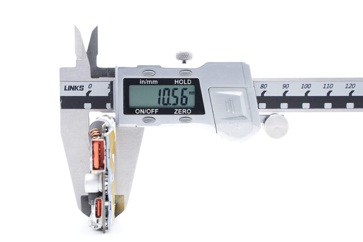
And the height is about 10.5mm (0.41 inches).
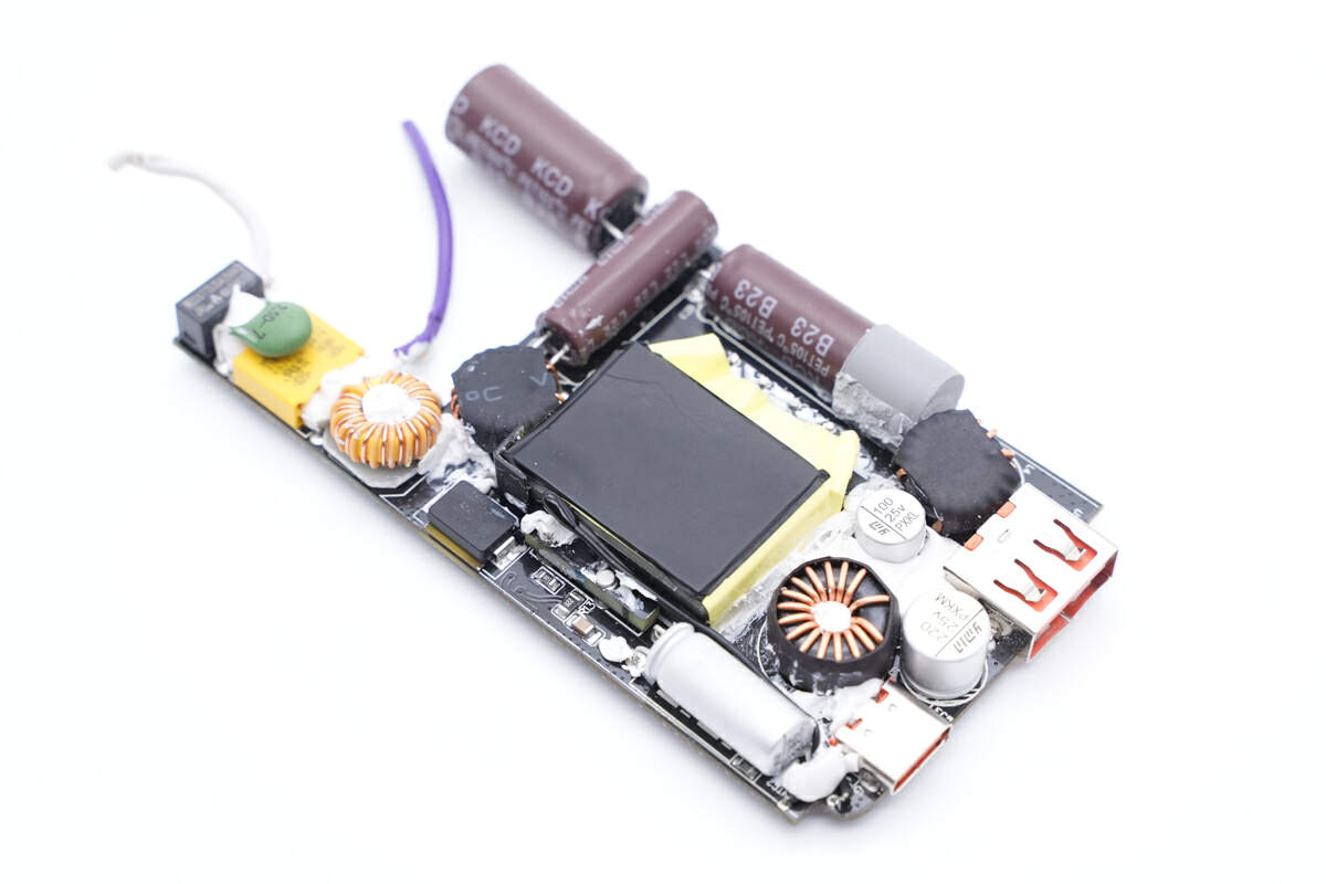
All components are placed horizontally to reduce the thickness.
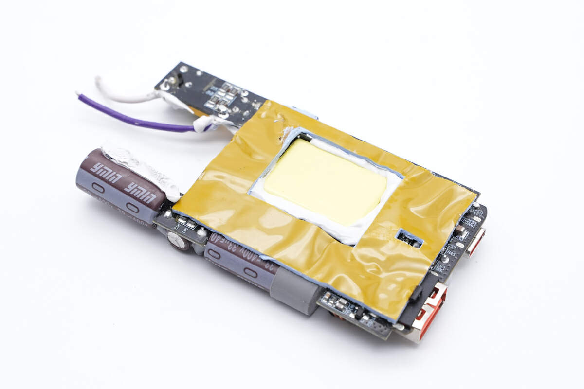
And the largest component, the transformer, is placed in the hollow of the PCB, the thermal pad is pasted around the transformer for heat dissipation.
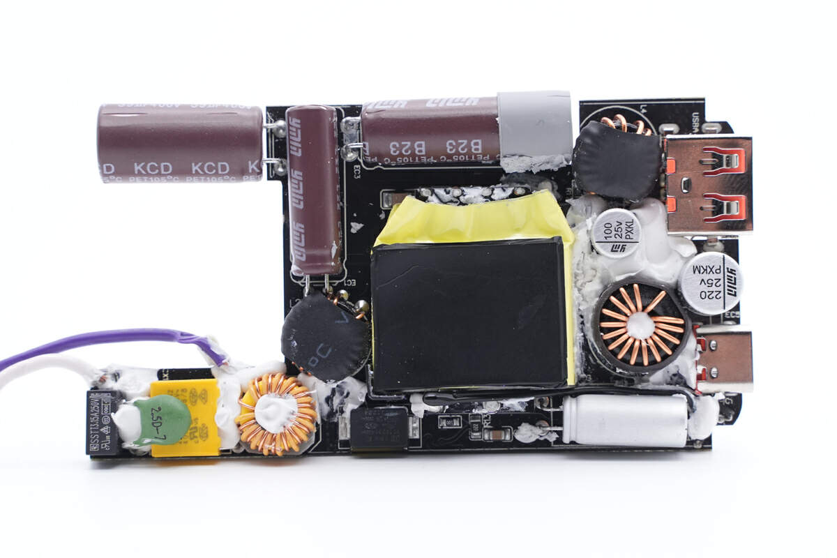
First, let's take a look at the front of the PCBA module. In the bottom left corner, we have the AC input end, which includes a fuse, NTC thermistor, safety X2 capacitor, and common mode choke, among other components. In the top left corner, we can see the high-voltage filtering capacitor, located right next to the planar transformer. On the right side, there is the secondary buck circuit, consisting of two inductors, filtering capacitor, and USB-A and USB-C sockets.
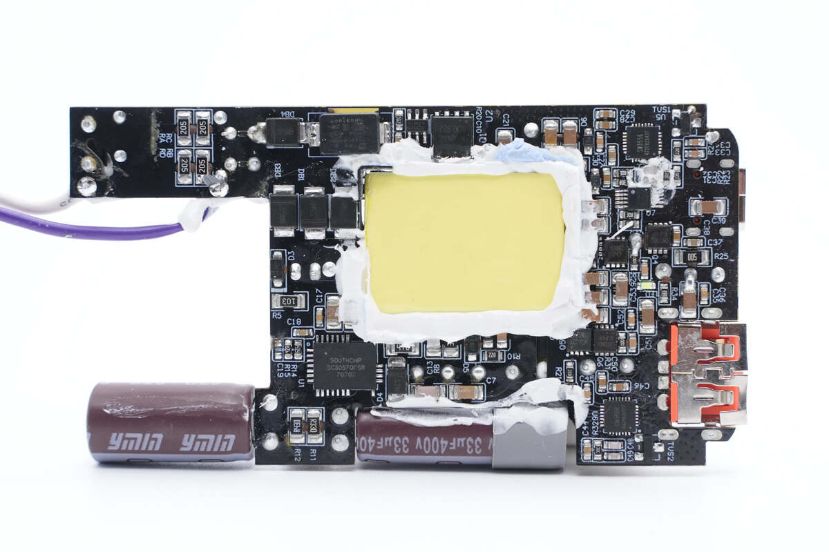
On the backside, there are the bridge rectifier, GaN IC, synchronous rectification controller, and buck chip.
ChargerLAB found it adopts QR flyback topology and is equipped with a synchronous rectification circuit to output the fixed voltage, then, the output circuit and protocol chip control the output power. Next, let’s introduce all components inside, starting from the input end.
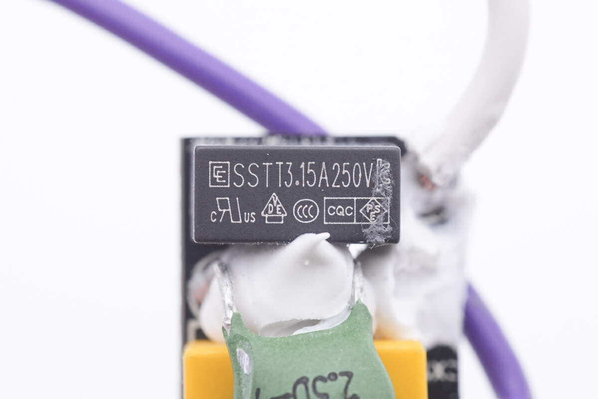
The input time-delay fuse is from CHEVRON. 3.15A 250V.
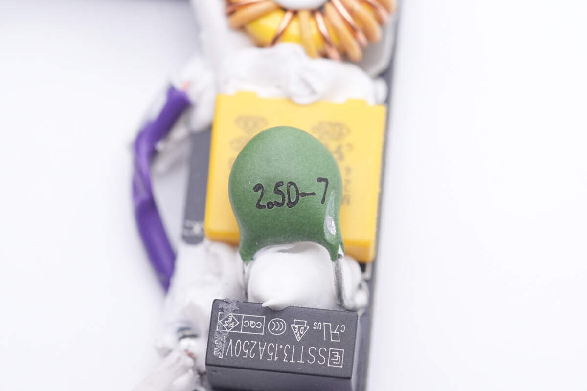
The NTC thermistor is printed with 2.5D-7, used to suppress the inrush current. "2.5D" indicates that it has a resistance of 2.5Ω at 25℃, while "7" represents a diameter of 7mm.
The safety X2 capacitor is from DGCX. 0.1μF.
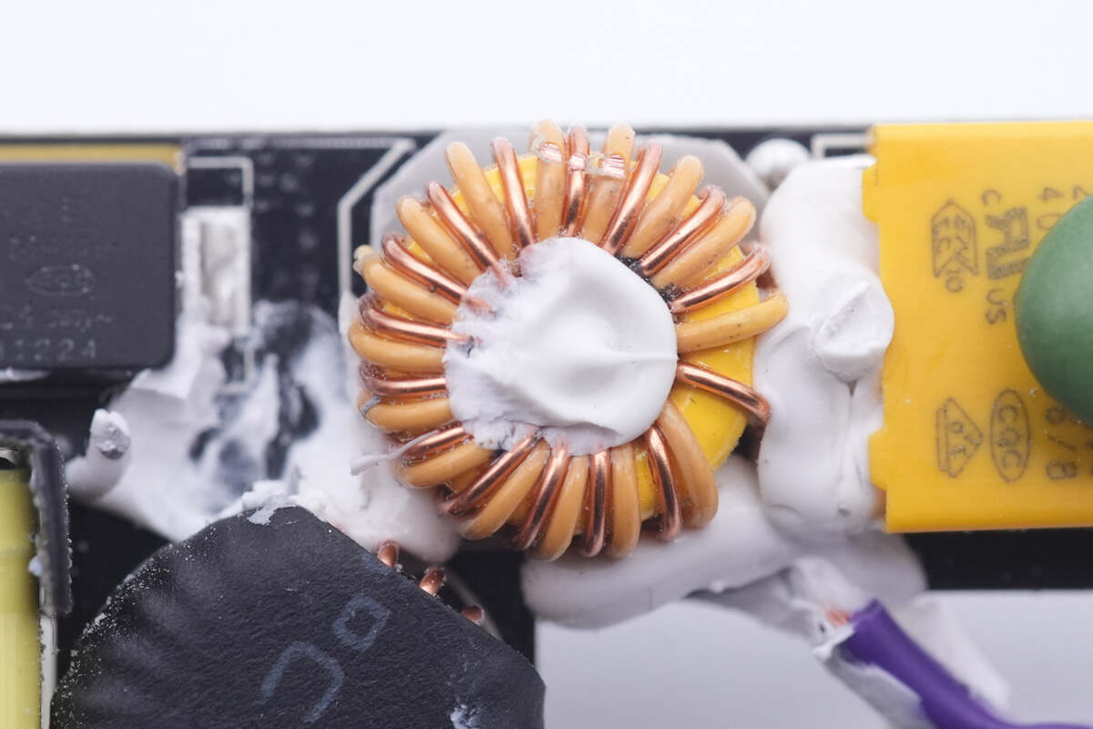
The common mode choke is next to the safety X2 capacitor.
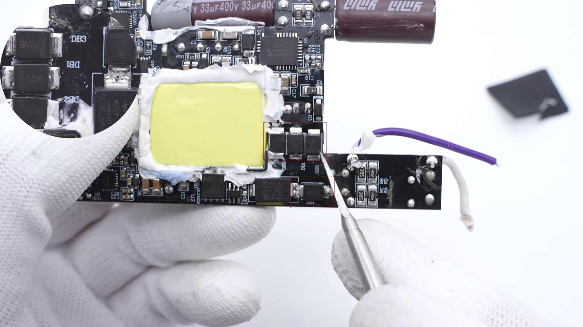
The bridge rectifier is composed of four diodes.
5A 1000V for each. Model is S5MB.
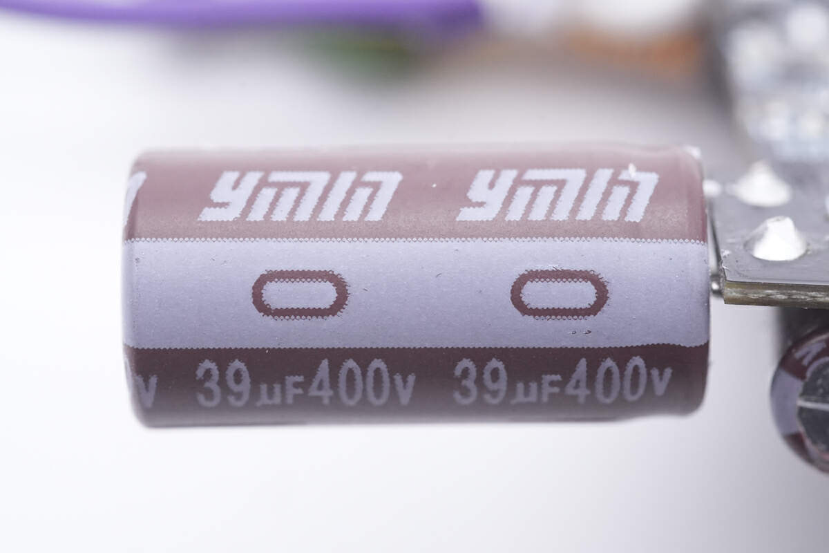
A total of three electrolytic capacitors are all from Yongming. The first one is 39μF 400V.
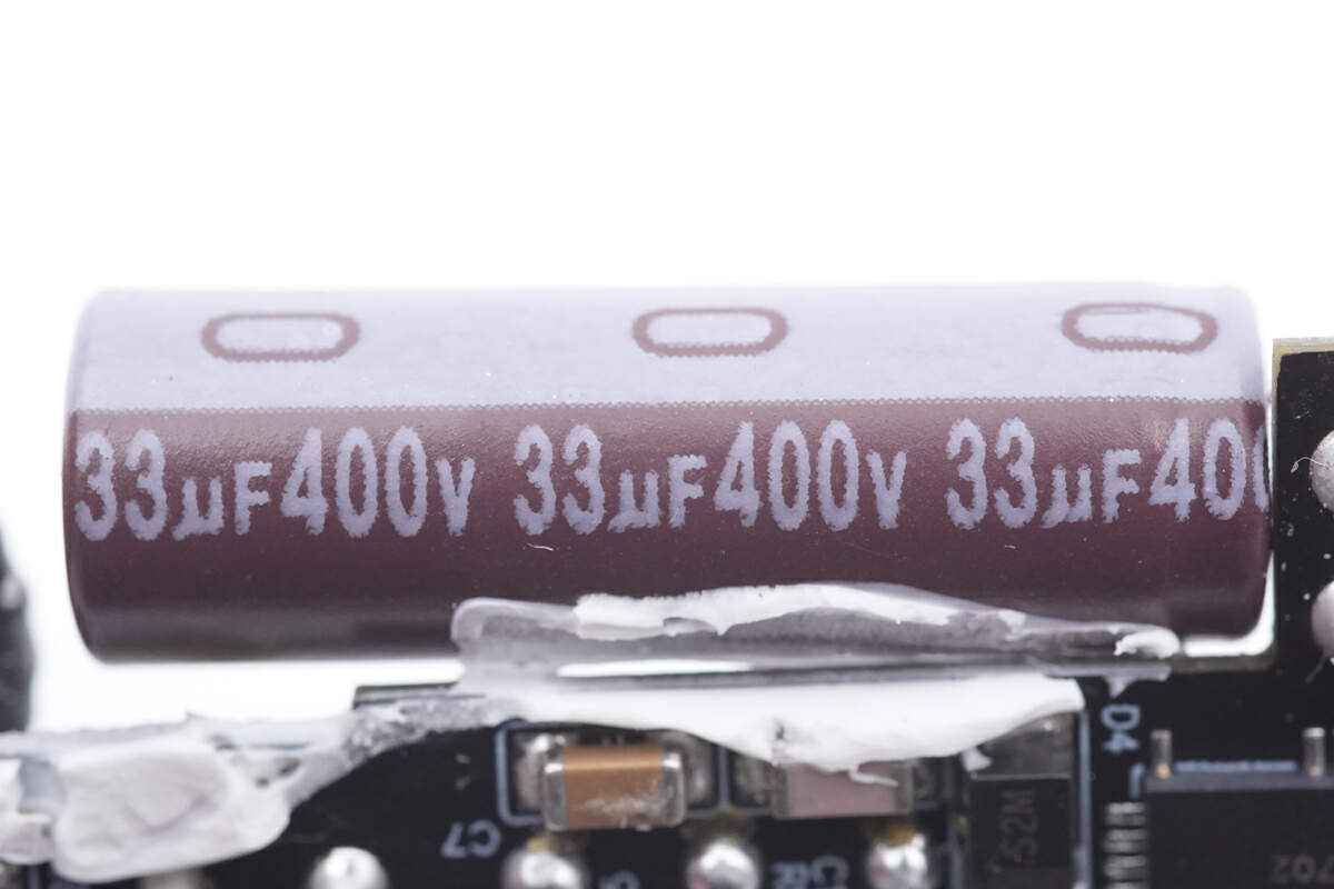
The second one is 33μF 400V.
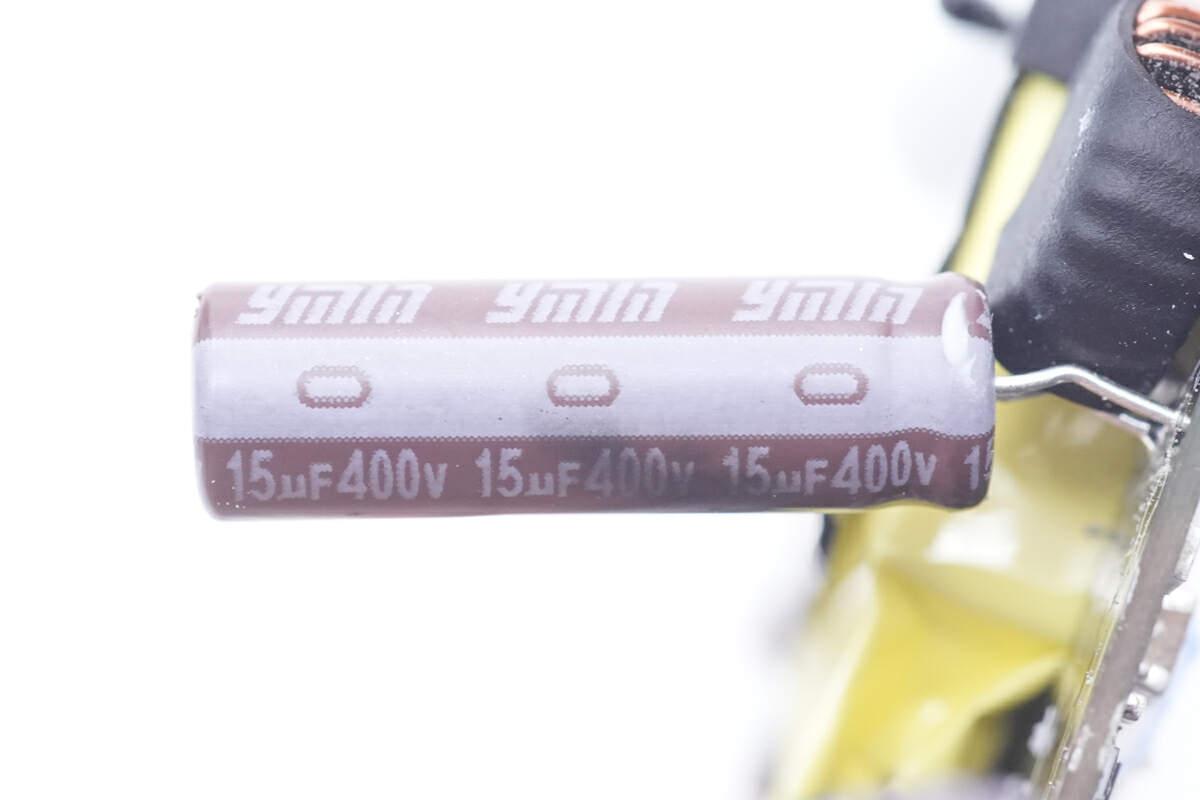
And the last one is 15μF 400V, 87μF in total.
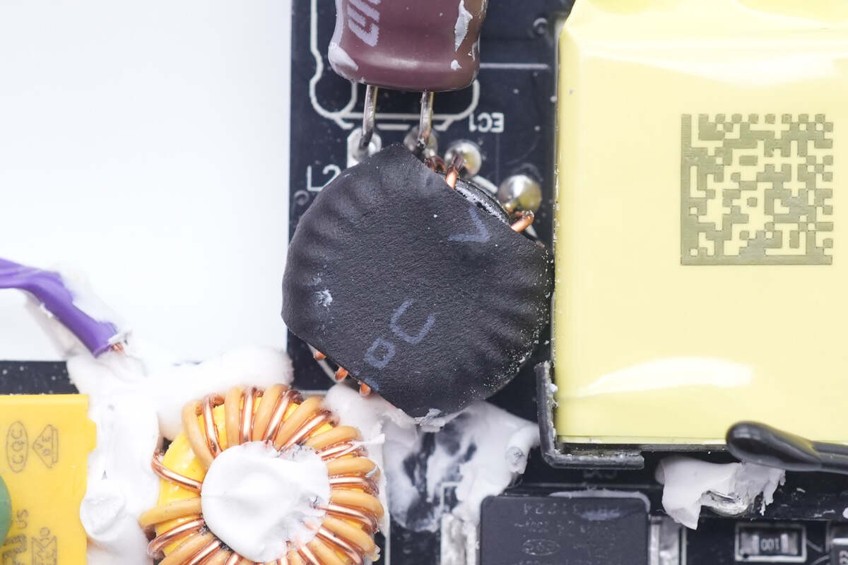
The differential mode choke is insulated by heat shrinkable tubing.
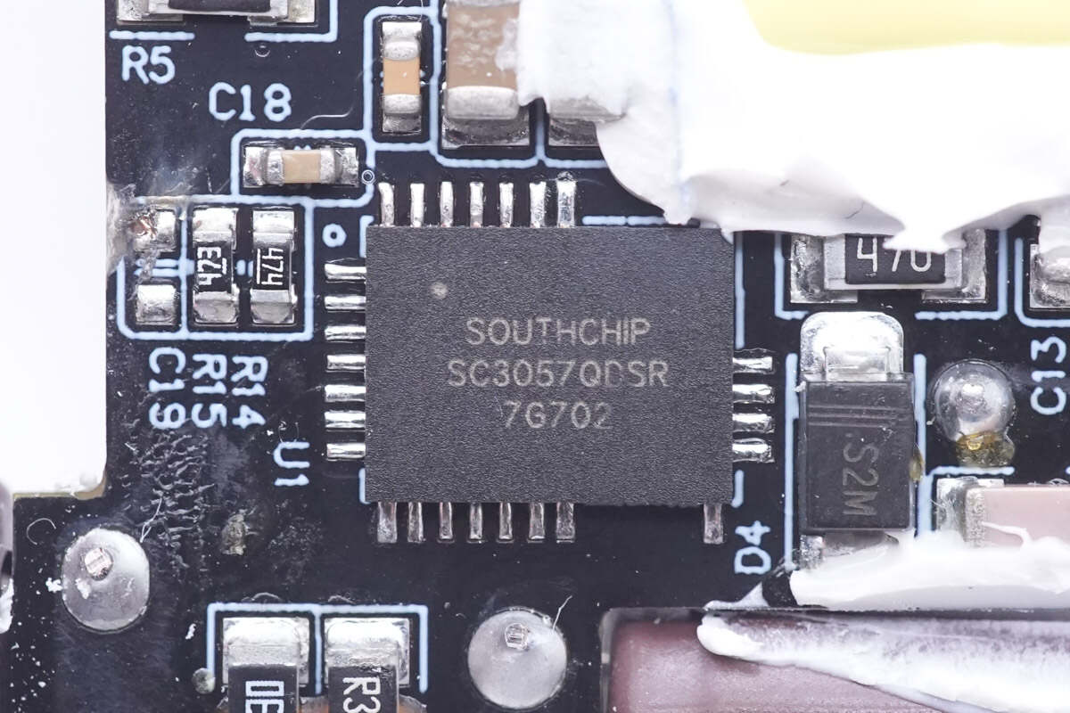
The master control chip of the charger adopts Southchip's GaN IC SC3057. This chip integrates high-performance multi-mode flyback controller, GaN driver, GaN FET, power supply and protection circuits. Simplify the number of external components and eliminate the parasitic elements of traditional drive wiring on high-frequency switching through package integration.
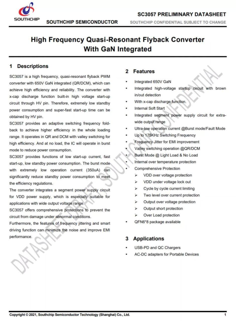
It also adopts a design that separates power wiring and control wiring to reduce the impact of high-frequency switching on the control loop, and optimizes the charger wiring design and electrical performance through optimized pad design, which simplifies design development. It has a built-in 165mΩ GaN FET, supports 175KHz switching frequency, and X-capacitor discharge.
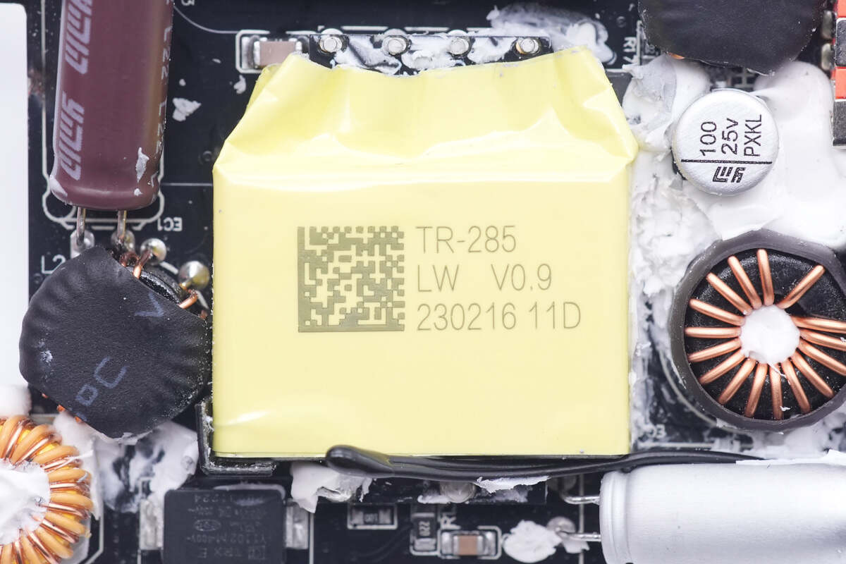
Here is the planar transformer, which is the key to make the charger ultra-slim.
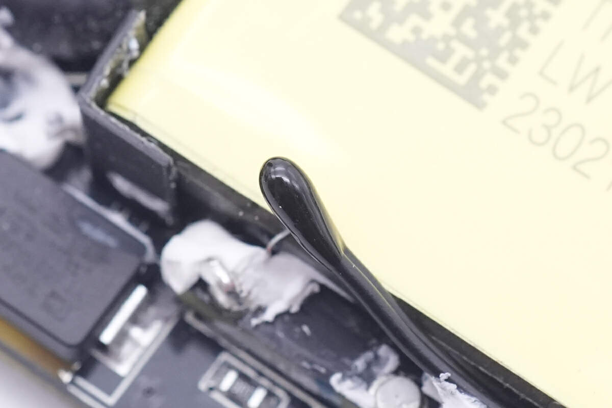
The thermistor is pasted on the side of the transformer to detect the internal temperature.
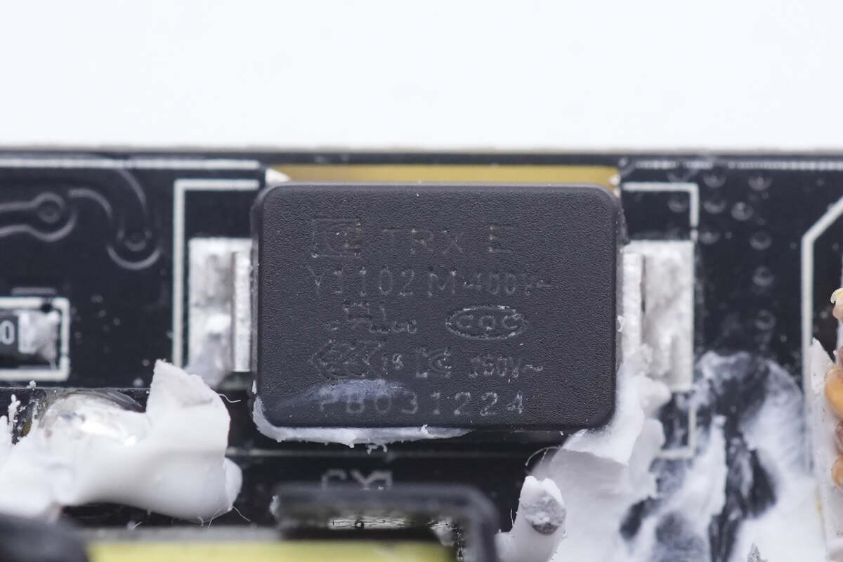
The SMD Y capacitor is from TRX, model TMY1102M, which features in small size and light weight, and are very suitable for high-density power supply products such as GaN charger.
TRX focuses on the R&D, production and sales of passive components, with a registered capital of 100 million yuan. It has two types of capacitor brands: SMD TRX and DIP TY capacitors. TRX will devote itself to the research of ceramic materials in order to provide customers with more solutions.
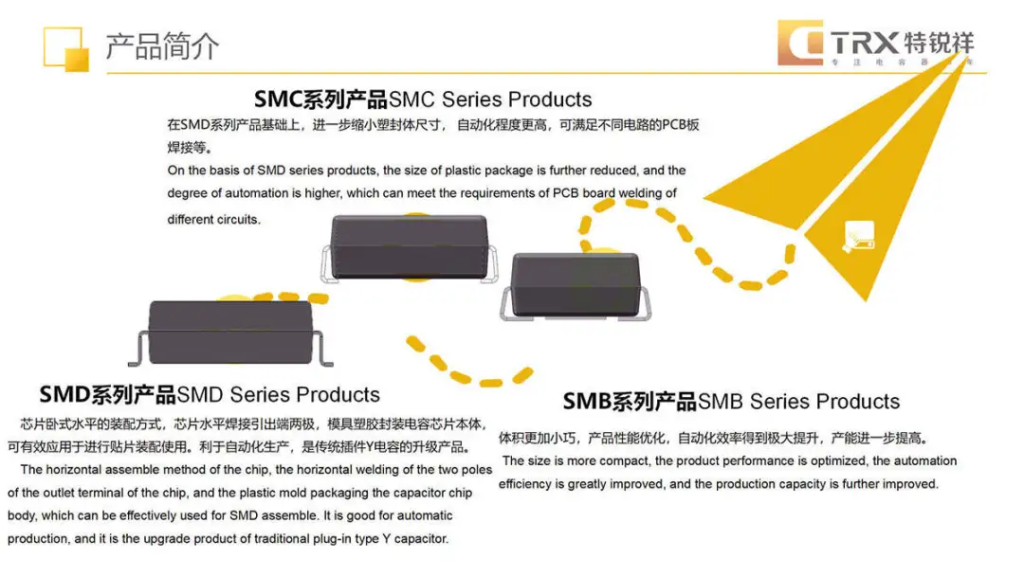
This is the introduction for TRX's products.
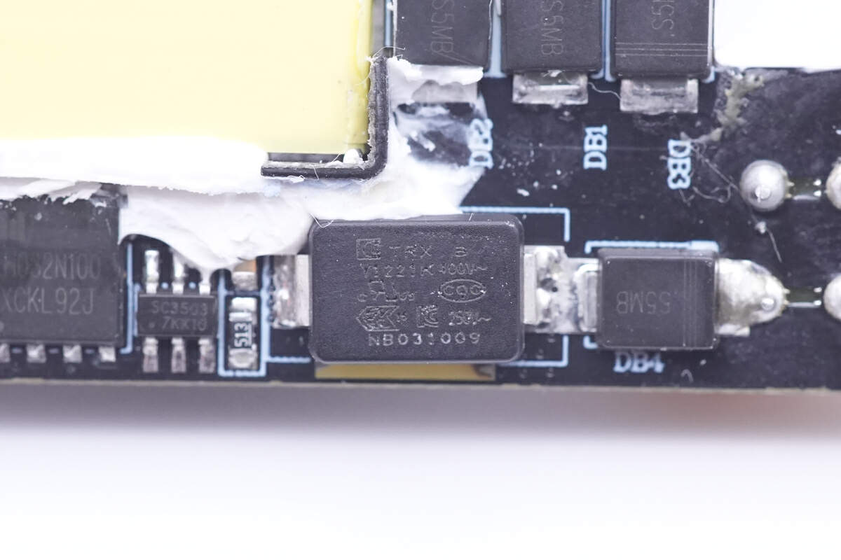
The other SMD Y capacitor is also from TRX, but the model is TMY1221K instead.
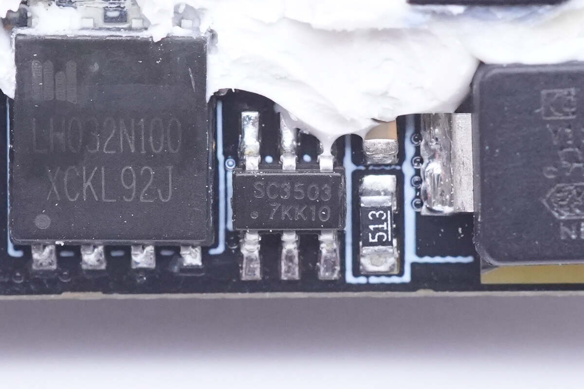
Then, let's move to the synchronous rectification circuit. The controller is from Southchip, model SC3503, which features in adaptive turn-on detection and fast turn-off. It does not need auxiliary coil for power supply, and the output voltage can be as low as 0V. The patented adaptive turn-on detection circuit avoids the synchronous rectifier from being mistaken as turned on. It is compatible with various MOS, has ultra-low static current, supports multiple operating modes, and supports both high-side and low-side synchronous rectification with very few peripheral components.
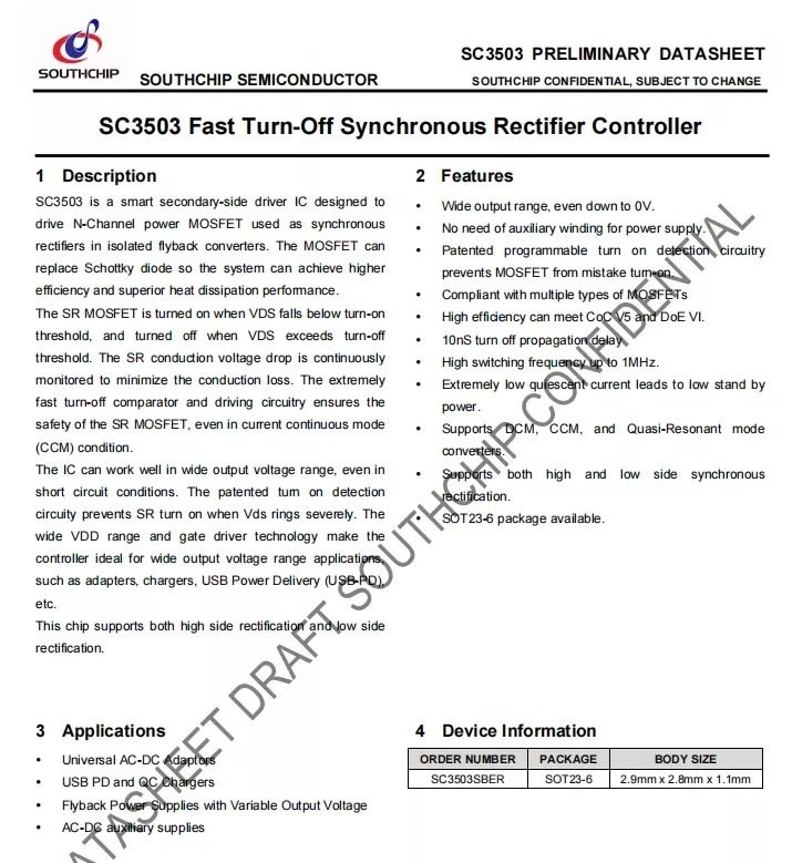
Here is all the information about Southchip SC3503.
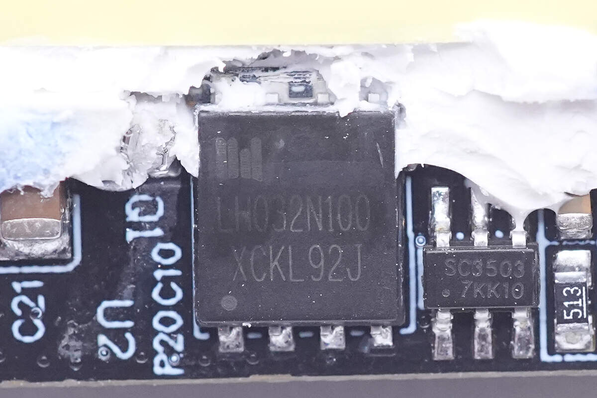
The synchronous rectifier is from LIHOMicro and adopts DFN5 x 6 package. Withstand voltage is 100V. Model is LH032N100.
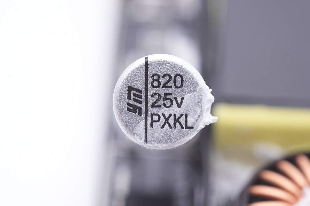
This solid capacitor for output filtering is from Yongming NPX series. 820μF 25V.
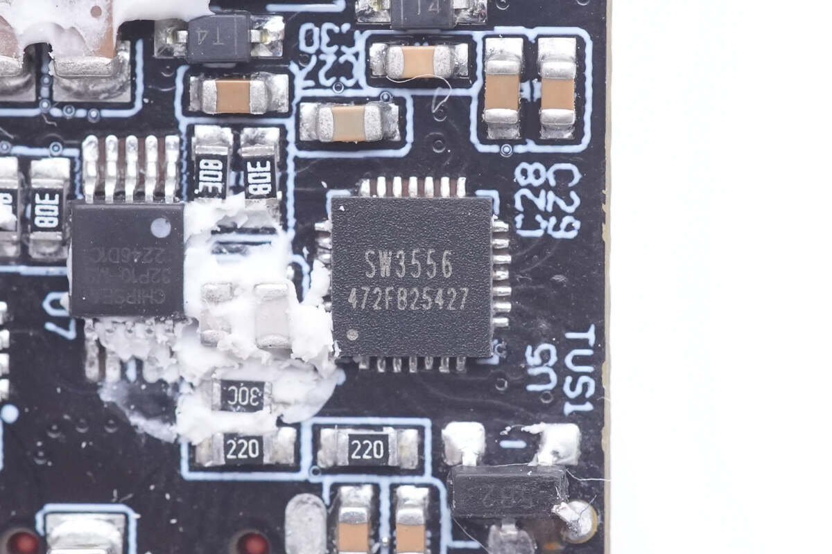
The protocol chips of both buck circuits are from Ismartware SW3556. It can control the output of dual USB-C ports and integrates a variety of fast charging protocols. It also supports a large current of 7A, independent current limiting. It supports driving low-voltage GaN FET, which can further improve the efficiency of the voltage reduction circuits, and reduce the size of the charger and its heat dissipation requirements.
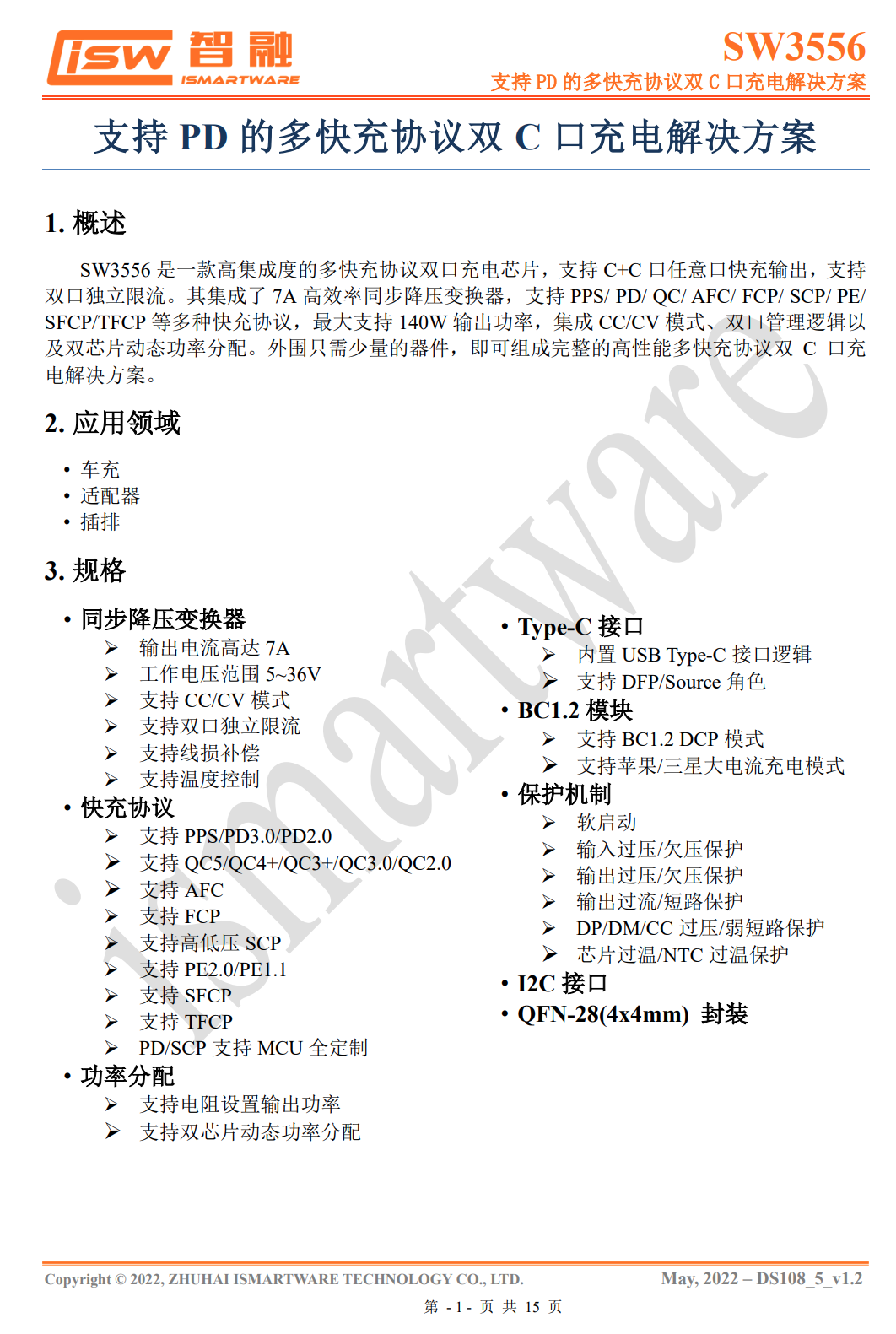
This chip features synchronous rectification buck topology and a 40V input, with a built-in synchronous rectification buck controller. When paired with simple peripheral devices such as silicon MOS or GaN FETs, inductors, and capacitors, it can support high power output of up to 140W. The built-in buck controller has a switching frequency of 125KHz and supports PFM/PWM mode operation to optimize conversion efficiency.
Moreover, it supports pin external resistance for configuring output power and dynamic power allocation without an external microcontroller, making peripheral devices more concise and cost-effective when developing multi-port fast charging products. It is suitable for product fields such as car chargers, multi-port chargers, and power strips.
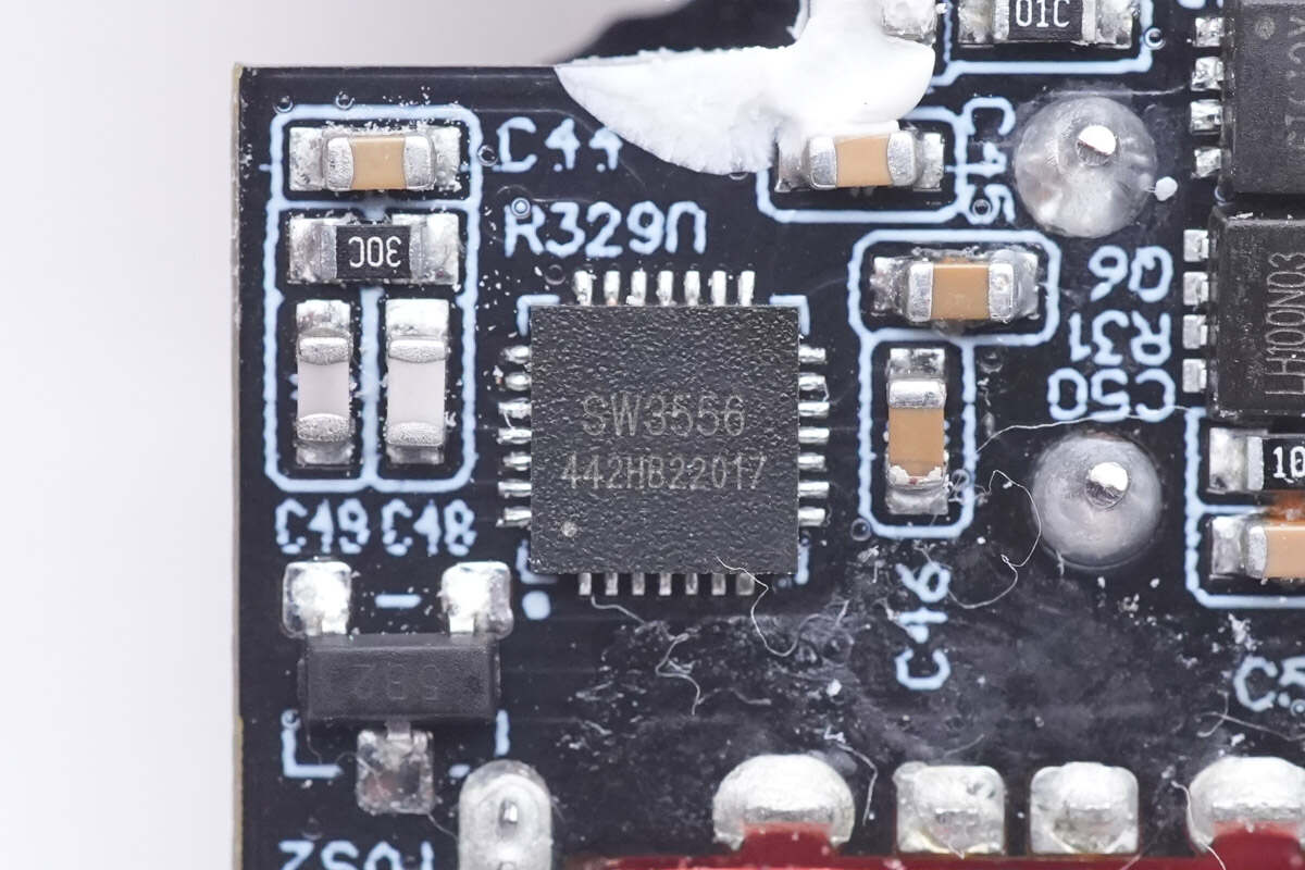
Here is the other one.
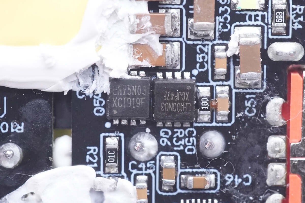
Those two buck MOSFETs are from LIHOMicro, with the respective models LH100N03 and LH75N03.

Finally, we have the output end.
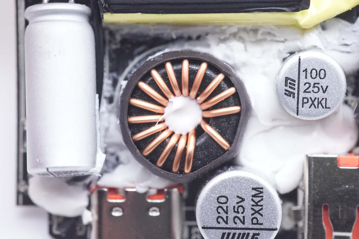
The buck inductor of USB-C output port is insulated with heat-shrinkable tubing.
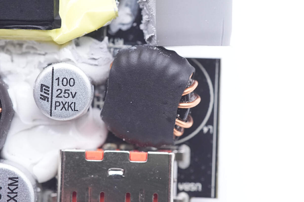
So is the one for USB-A port.
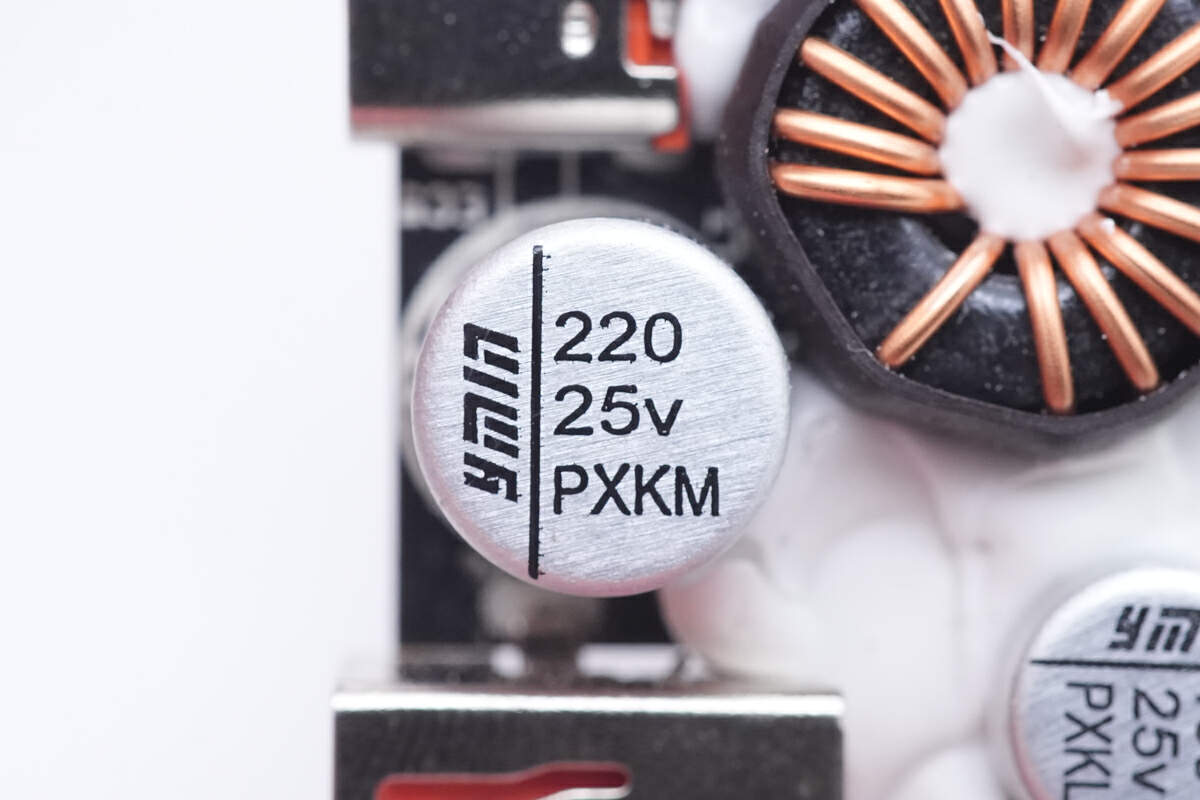
This solid capacitor for the USB-C port is from Yongming NPX series. 220μF 25V.
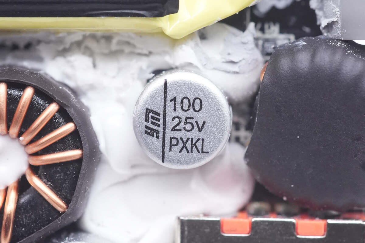
And the other solid capacitor for USB-A is also from Yongming. 100μF 25V.
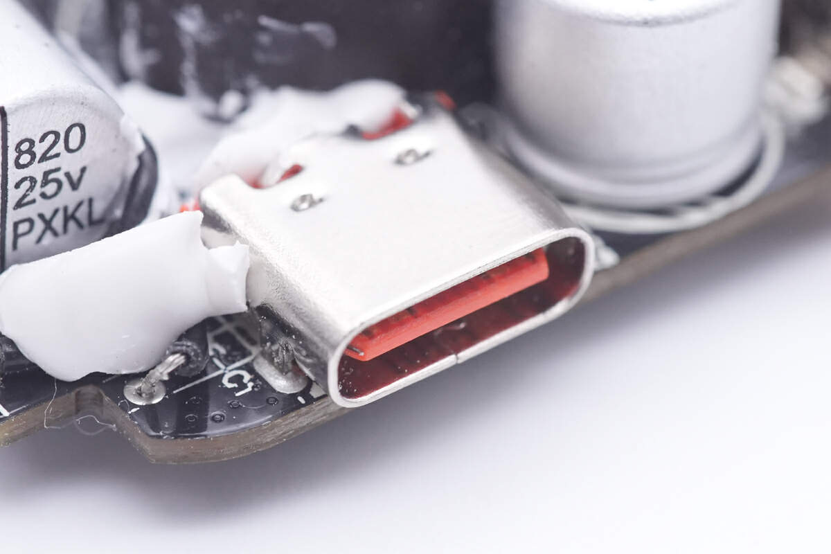
The USB-C socket is secured by through-hole soldering.
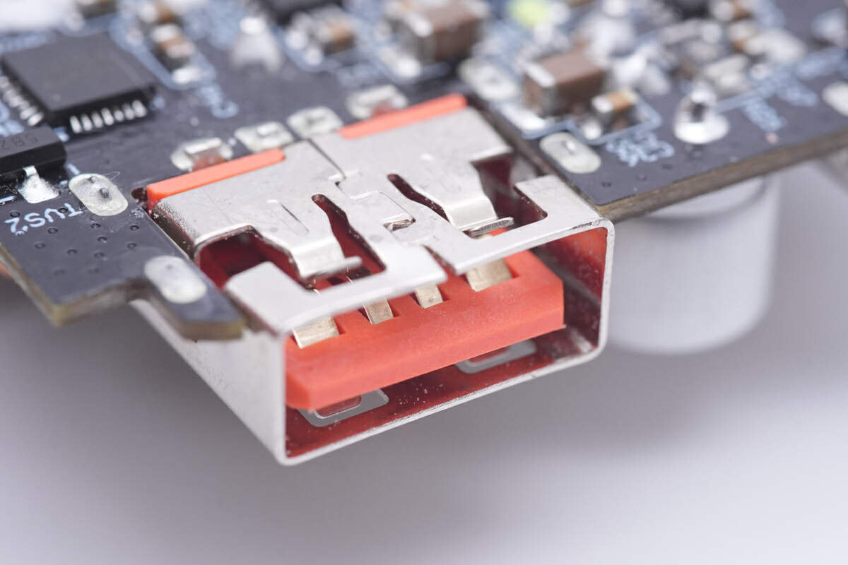
The same applies to the USB-A, and the positive and negative pins are widened for high-current fast charging.
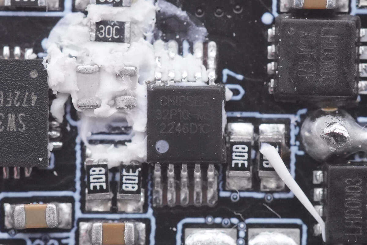
This 8-bit MCU, model CSU32P10, is from Chipsea and adopts MSOP10 package, used to control the output power and overheating protection.
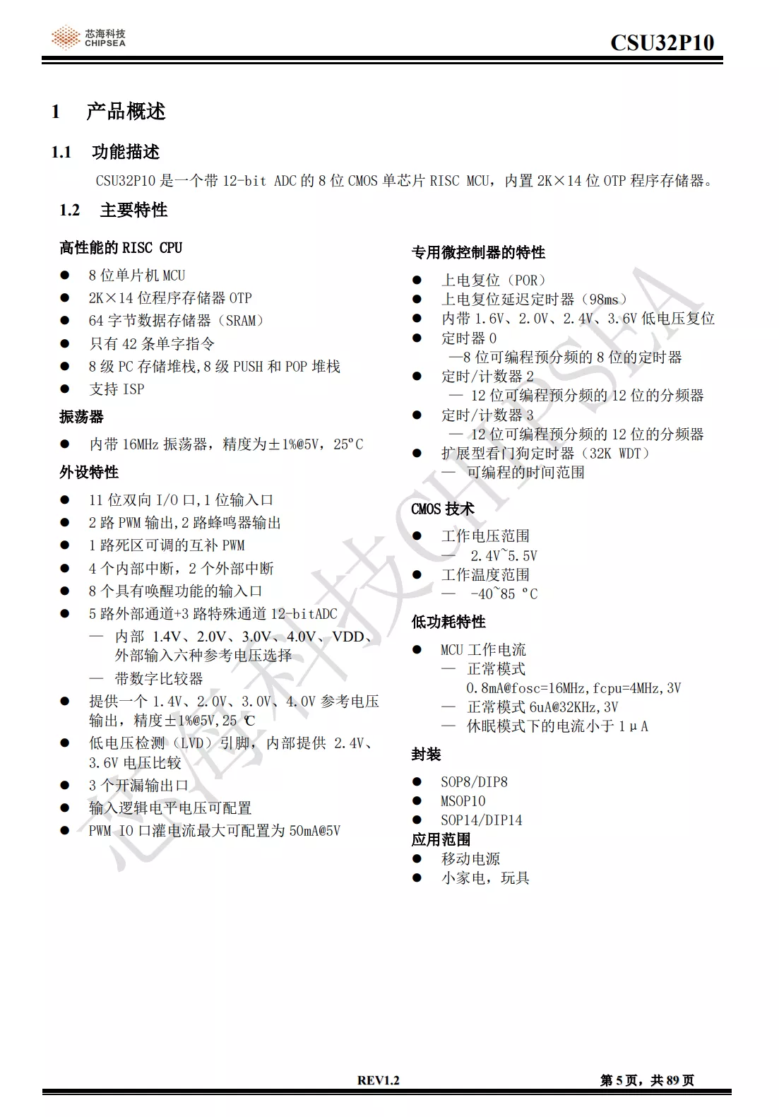
Here is all the information about Chipsea MSOP10.
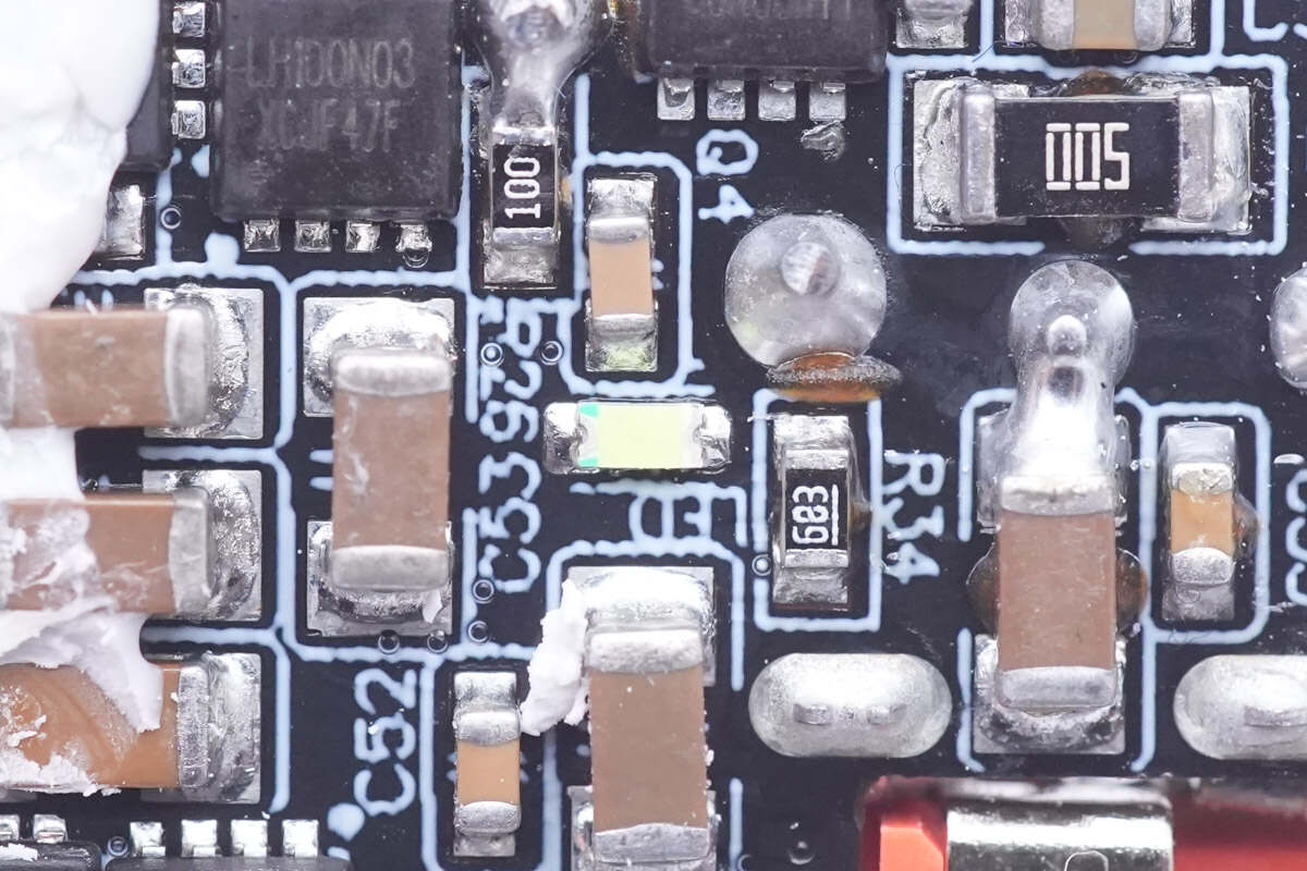
And this is the LED light we saw on the front.
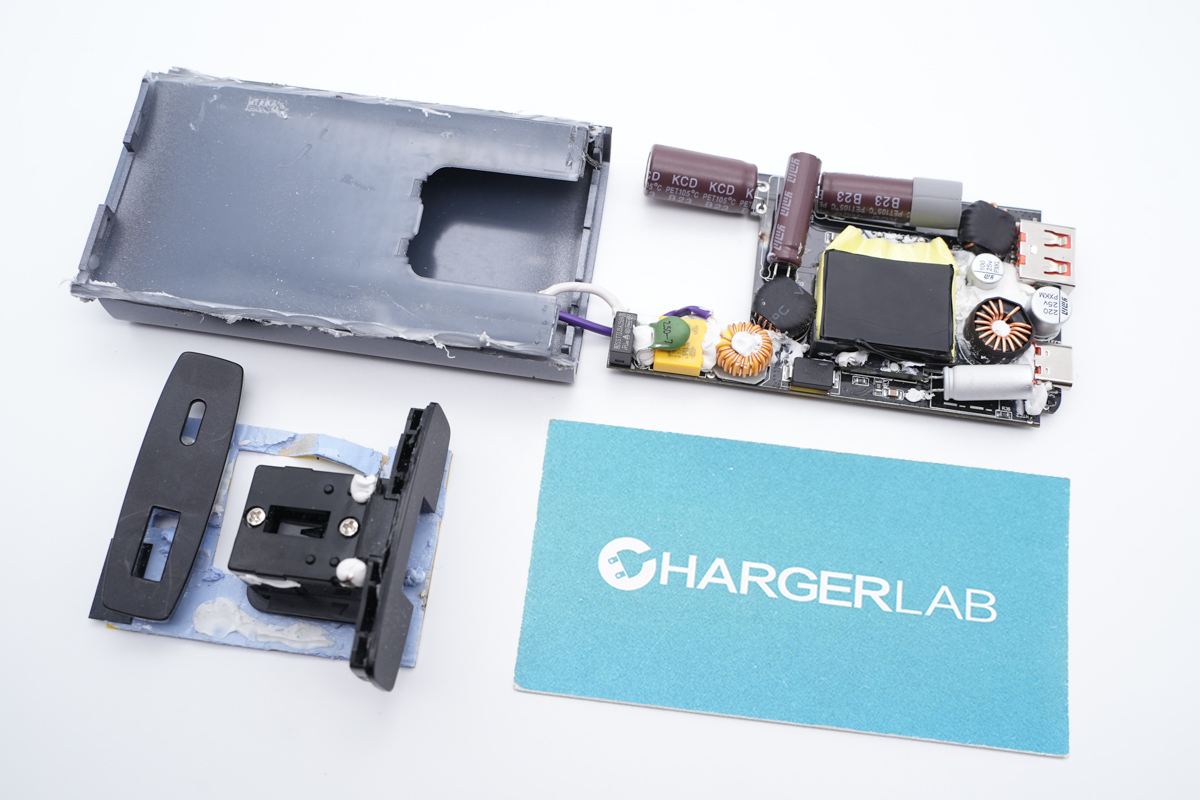
One last look at all the components of this Baseus 65W Ultra-Slim GaN Charger.
Summary of ChargerLAB
Thanks to the planar transformer and compact design of internal components, it can fit into your pocket easily. Unlike most PD chargers, the USB-A port provides up to 60W output power. With the other USB-C port, it can charge your primary device and some accessories at the same time when you're traveling.
Related Articles:
1. Ultra-Slim & GaN | Teardown of Baseus 65W Charger (Video)
2. Teardown of Baseus 140W PD3.1 GaN 5 Pro Fast Charger (2C1A)
3. Teardown of Baseus PowerCombo Pro 40W 6-in-1 GaN Power Strip

