Introduction
At 8 pm Eastern time on August 12th, Trump and Musk chatted for two hours on X, during which Trump pulled out a Chinese Anker brand power bank to charge his phone. This power bank is from the MagGo series, model A1654, and has a single USB-C port that supports 20W input and 27W output. The wireless charging power can be up to 15W, and it also comes in four colors: black, white, blue, and purple, making it easy to match with mobile phones of different colors.
There is an LCD on the side of the power bank, which can show the remaining power, output status, and input status, as well as the remaining usage time and remaining charging time. It uses Anker's independently developed Qi2 wireless charging module to reduce energy loss and improve charging efficiency. It comes with a bracket, which can be used as a phone stand after adsorbing, allowing the phone to be used horizontally or vertically. It also supports charging and discharging at the same time and can be used as a wireless charger.
The power bank has a built-in distance sensor, which can automatically start wireless charging after the phone is attached. Its battery capacity is 10000mAh. Next, let's take it apart to see its internal components and structure.
Product Appearance
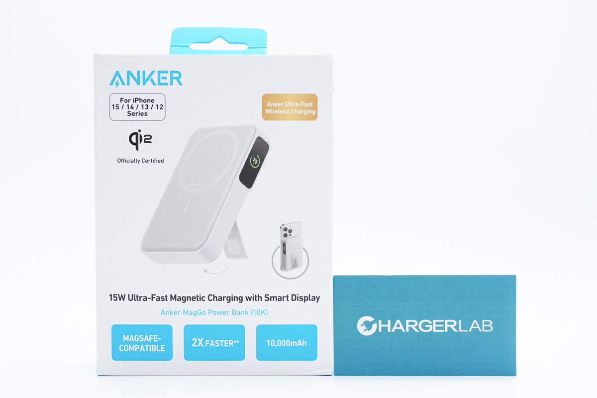
The front of the box is printed with ANKER, the appearance of the power bank, and it is suitable for the iPhone 12~15 series. It has passed the Qi2 certification, and the words MagSafe compatible, 2X faster, and 10000mAh are printed on the bottom.
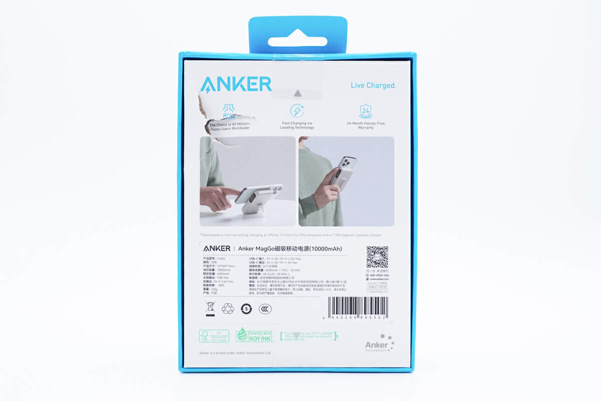
The back of the box shows two usage scenarios and some specs info are printed below.
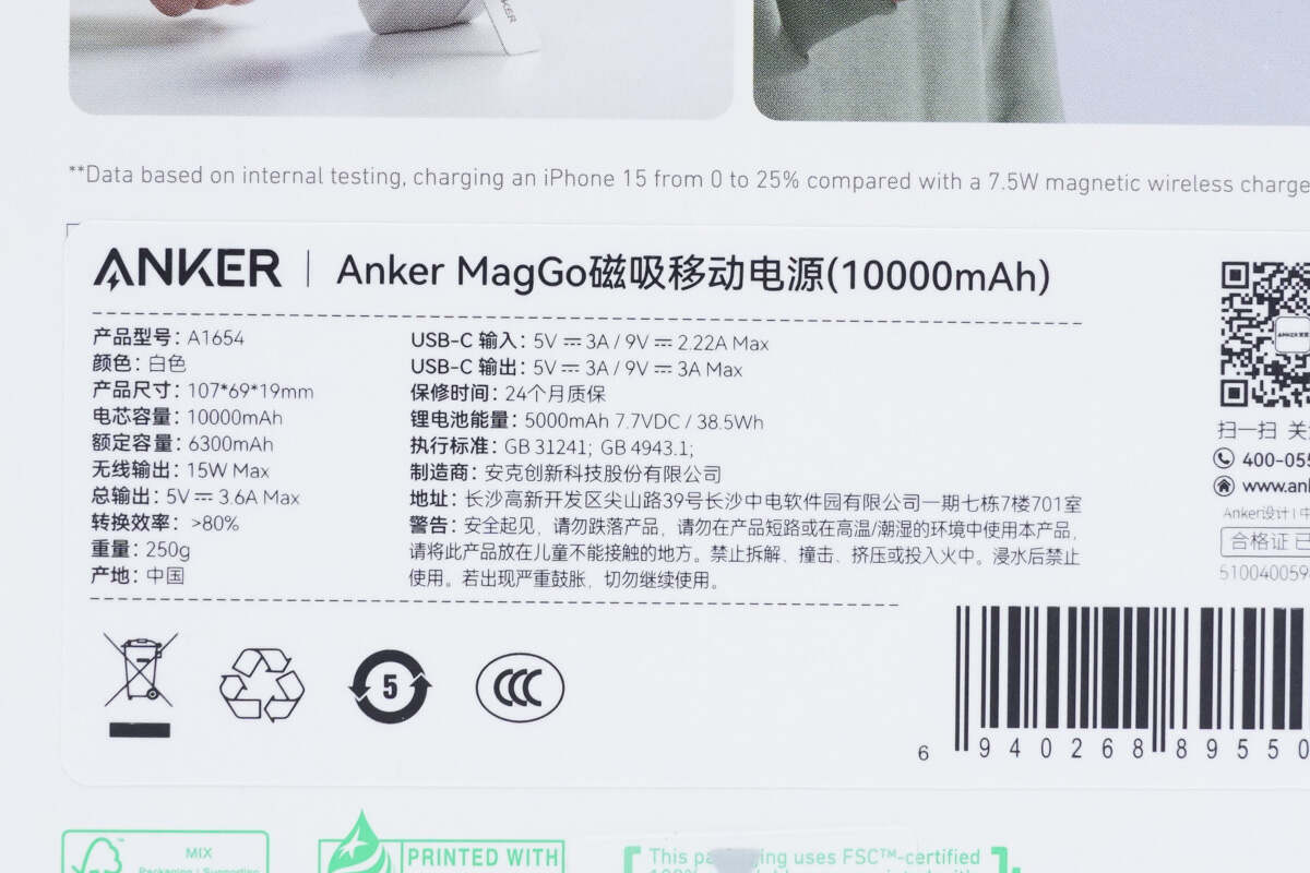
Model is A1654. The color is white. Its size is 107 x 69 x 19 mm (4.21 x 2.72 x 0.75 inches). Its battery capacity is 10000mAh. The rated capacity is 6300mAh. The Lithium battery energy is 5000mAh 7.7VDC/38.5Wh. The USB-C can support input of 5V 3A and 9V 2.22A. The USB-C can support output of 5V 3A and 9V3A. The maximum wireless output power is 15W. The total output is 5V 3.6A. The conversion efficiency is above 80%. Its weight is 250 g (8.82 oz).
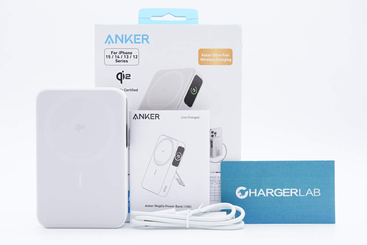
The box contains the Anker MagGo power bank, a cable, and some documents.
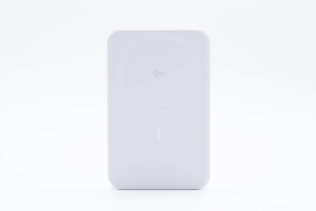
There is a magnetic wireless charging panel and the Qi2 logo printed on the front.
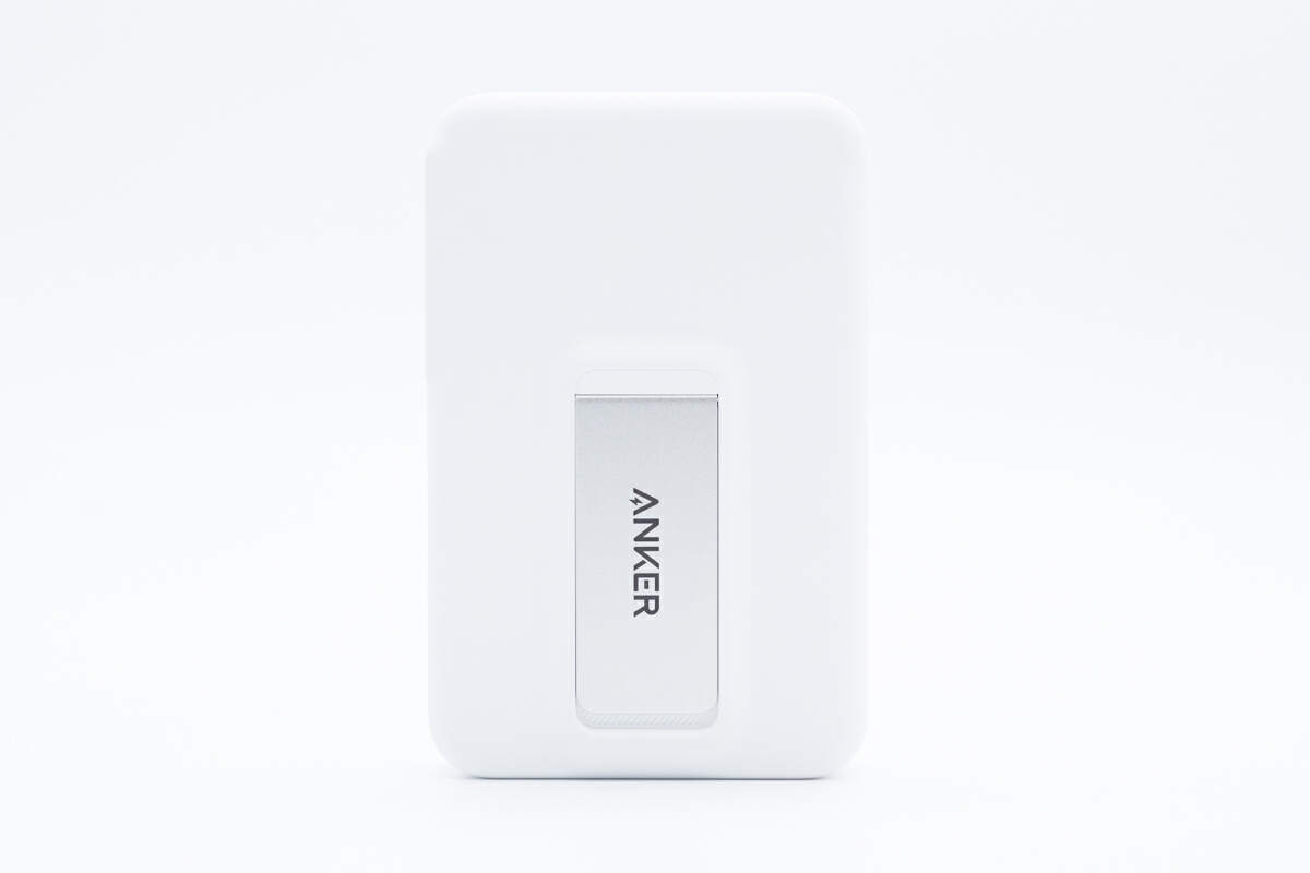
There is an aluminum alloy foldable bracket on the back with the ANKER logo printed on it.
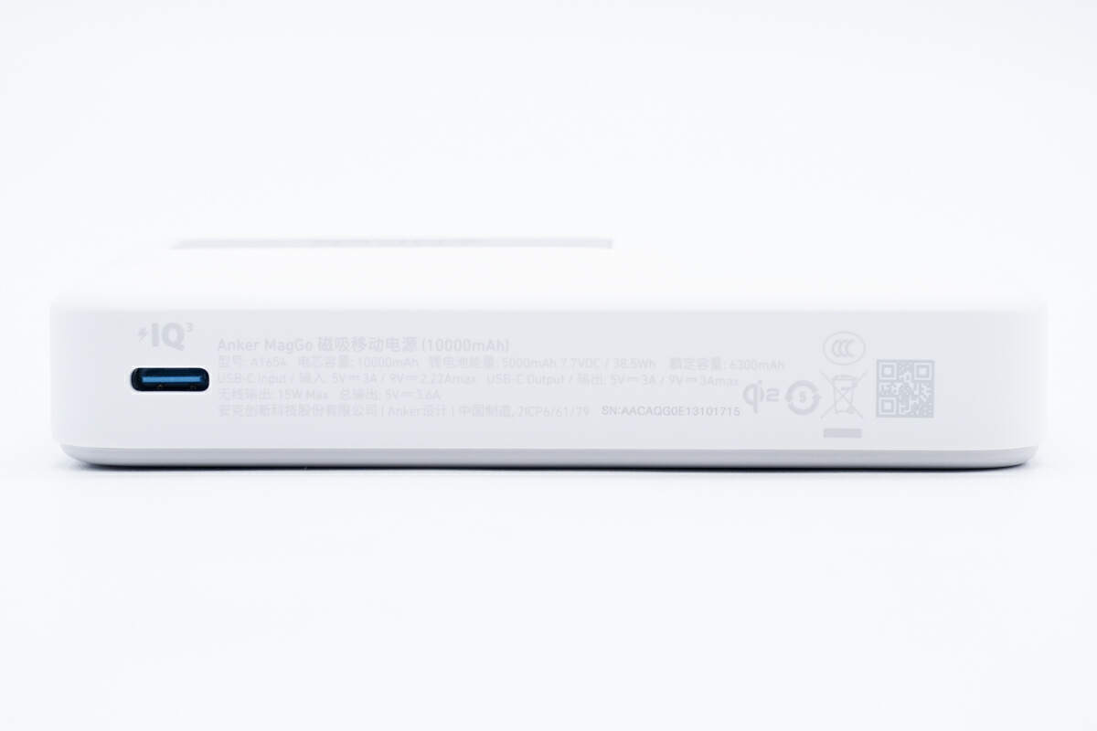
There is a USB-C port on the side, and the specs info are also printed on it.
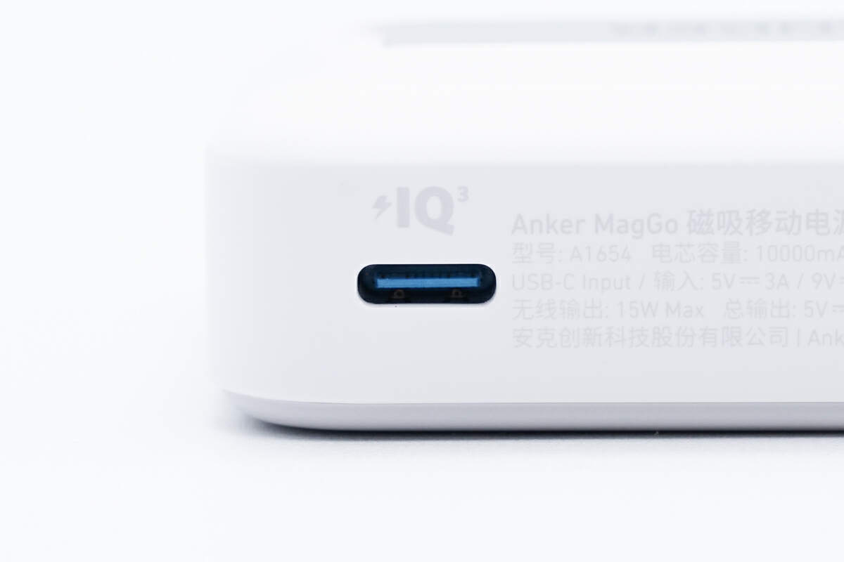
The USB-C port is blue.
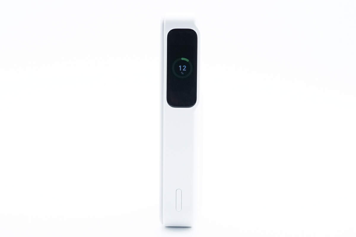
The display can show the remaining power after being turned on, and there is a power button below.
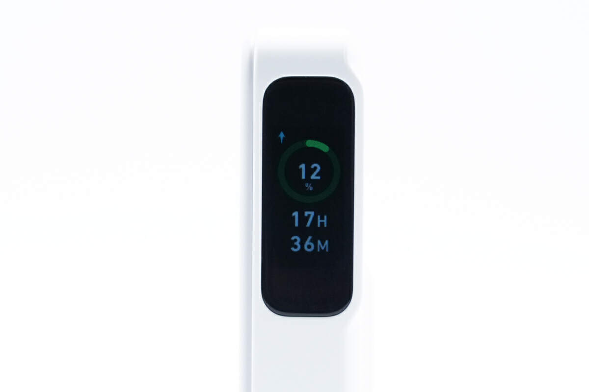
Below the remaining power is the remaining usage time.
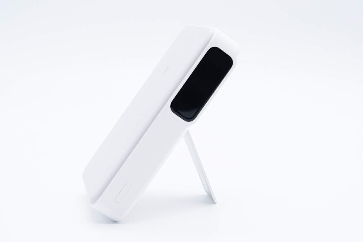
Open the bracket and the power bank can be supported steadily.
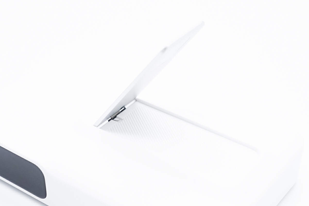
There is a spring inside the bracket, which is fixed by magnets.
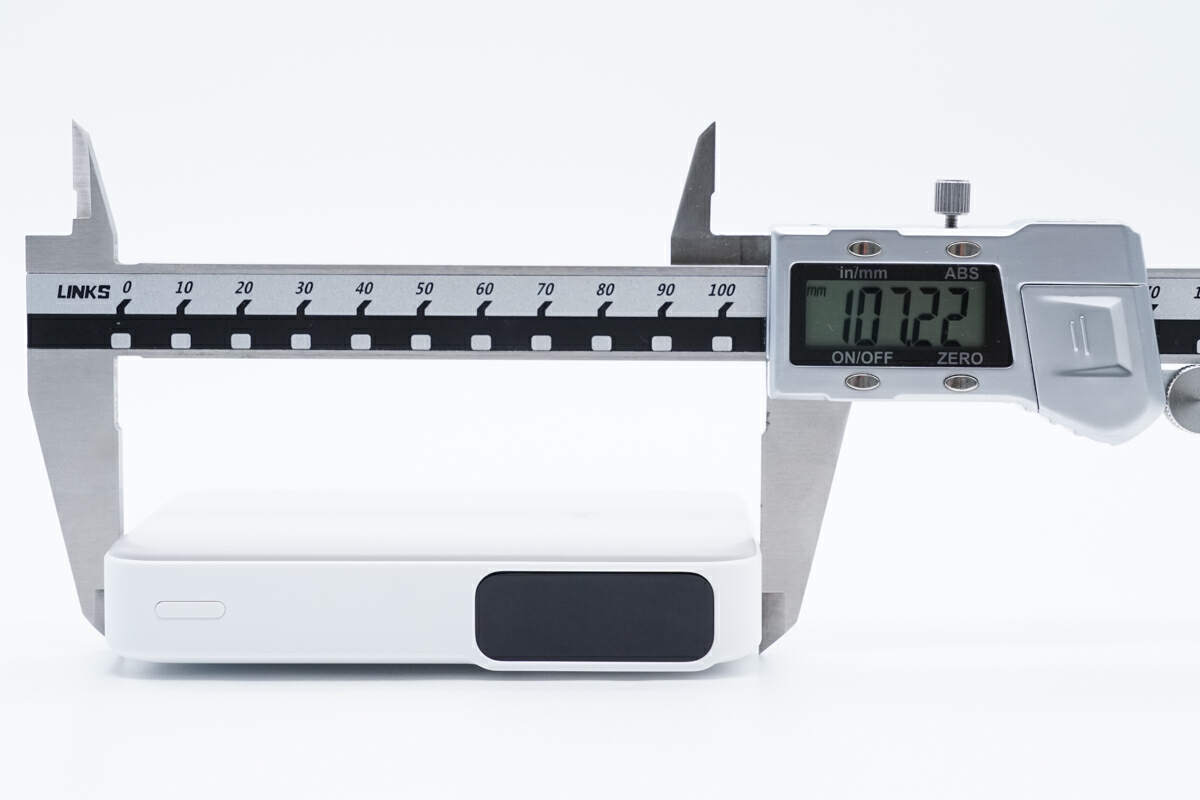
The length of the power bank is about 107 mm (4.21 inches).
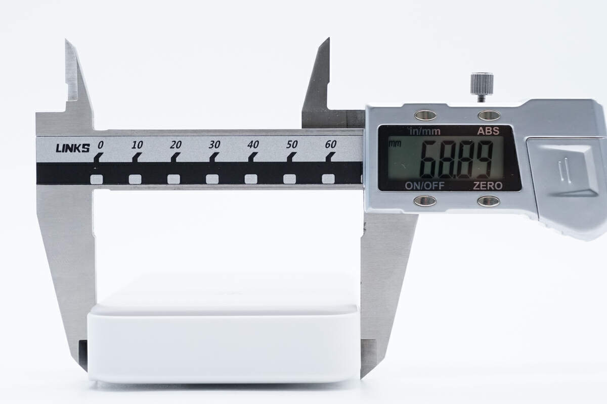
The width is about 69 mm (2.72 inches).
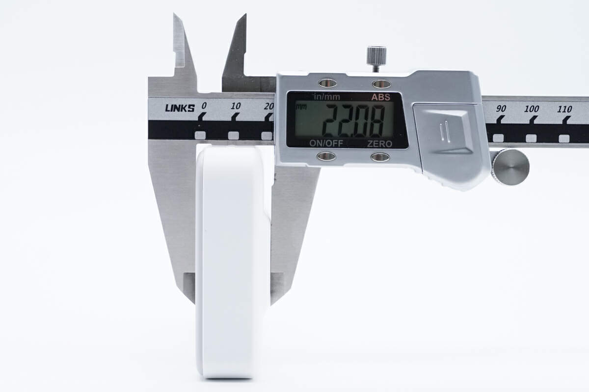
The thickness is about 22 mm (0.87 inches).

That's how big it is in the hand.
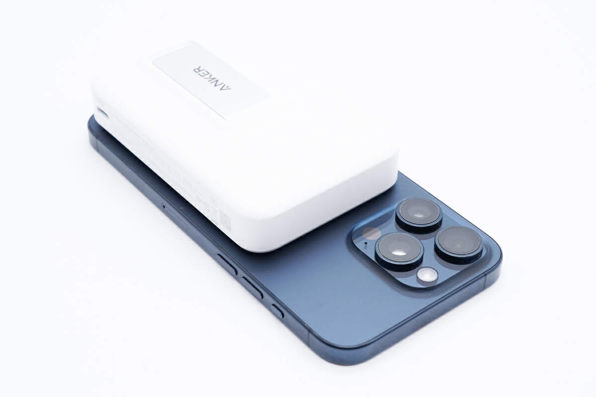
Use it to charge the iPhone 15 Pro Max, it will not block the camera.
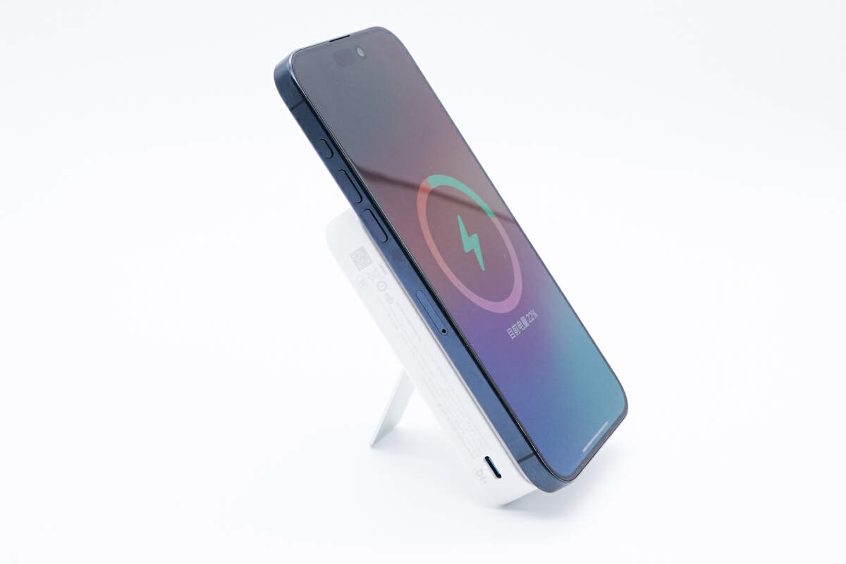
And it can support itself and the phone steadily through the bracket.
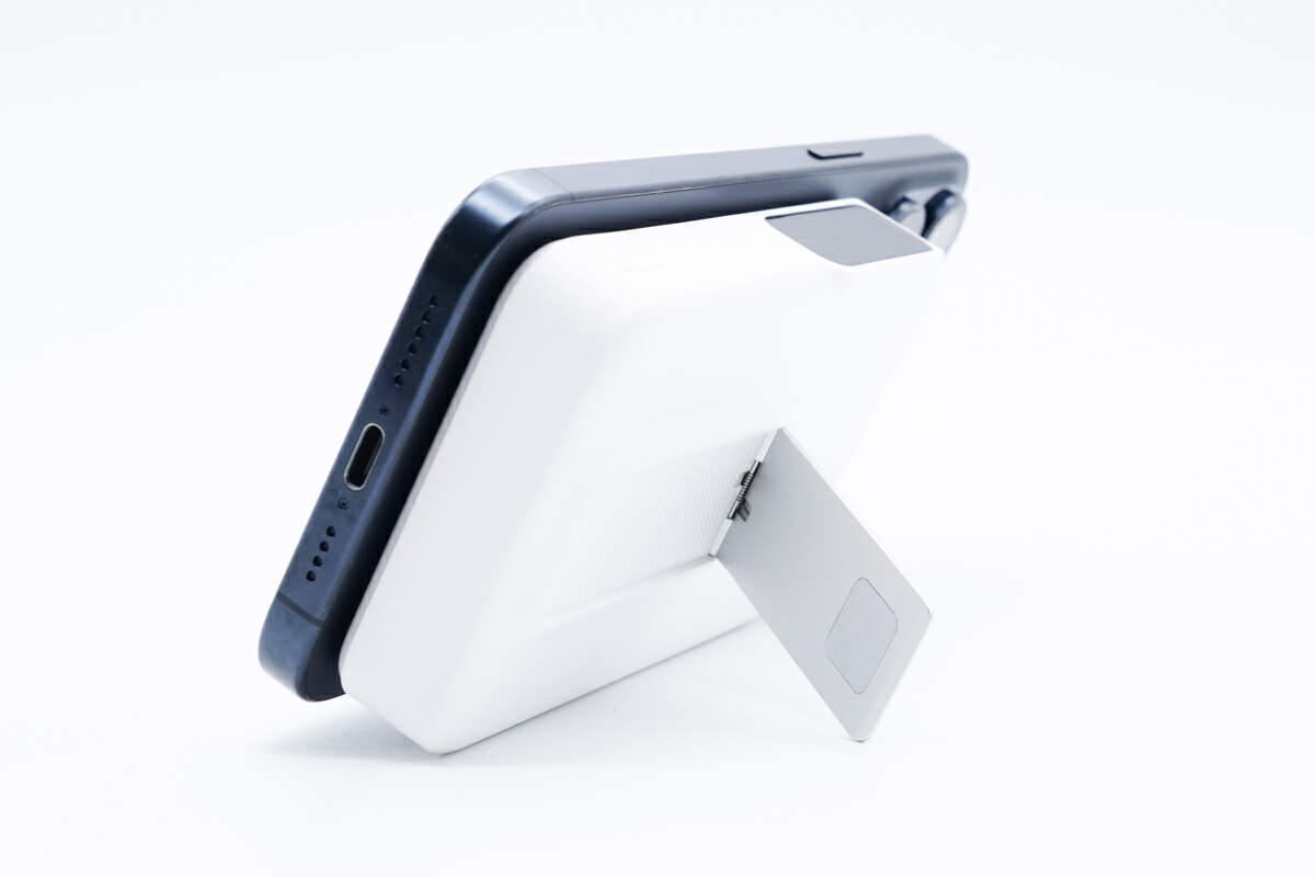
It can also be stably supported when placed horizontally.
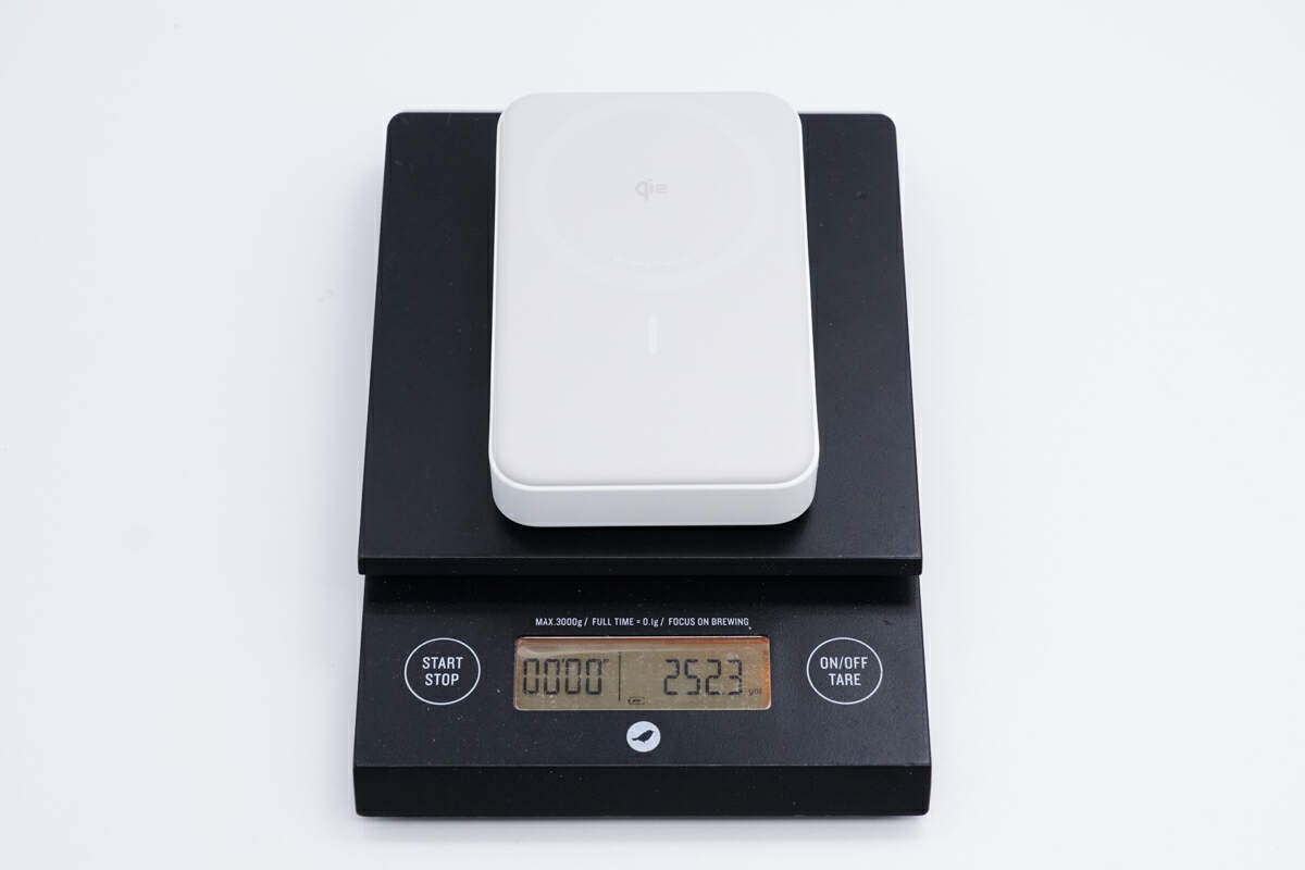
The weight is about 252 g (8.89 oz).
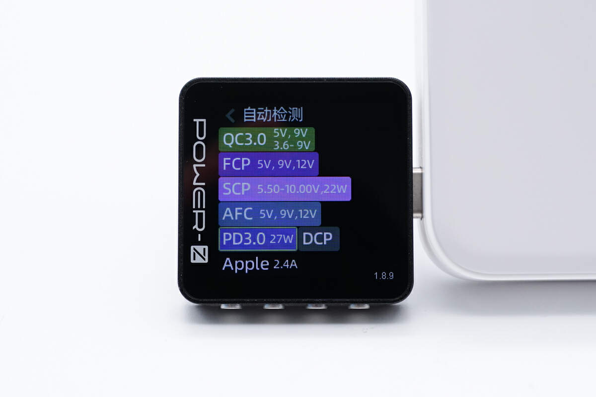
The ChargerLAB POWER-Z KM003C shows the USB-C port can support QC3.0, FCP, SCP, AFC, PD3.0, DCP, and Apple 2.4A charging protocols.
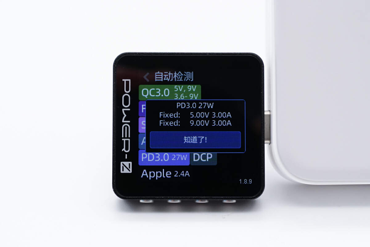
And it has two fixed PDOs of 5V 3A and 9V 3A.
Teardown
Next, let's start to take it apart and take a look at the internal components.
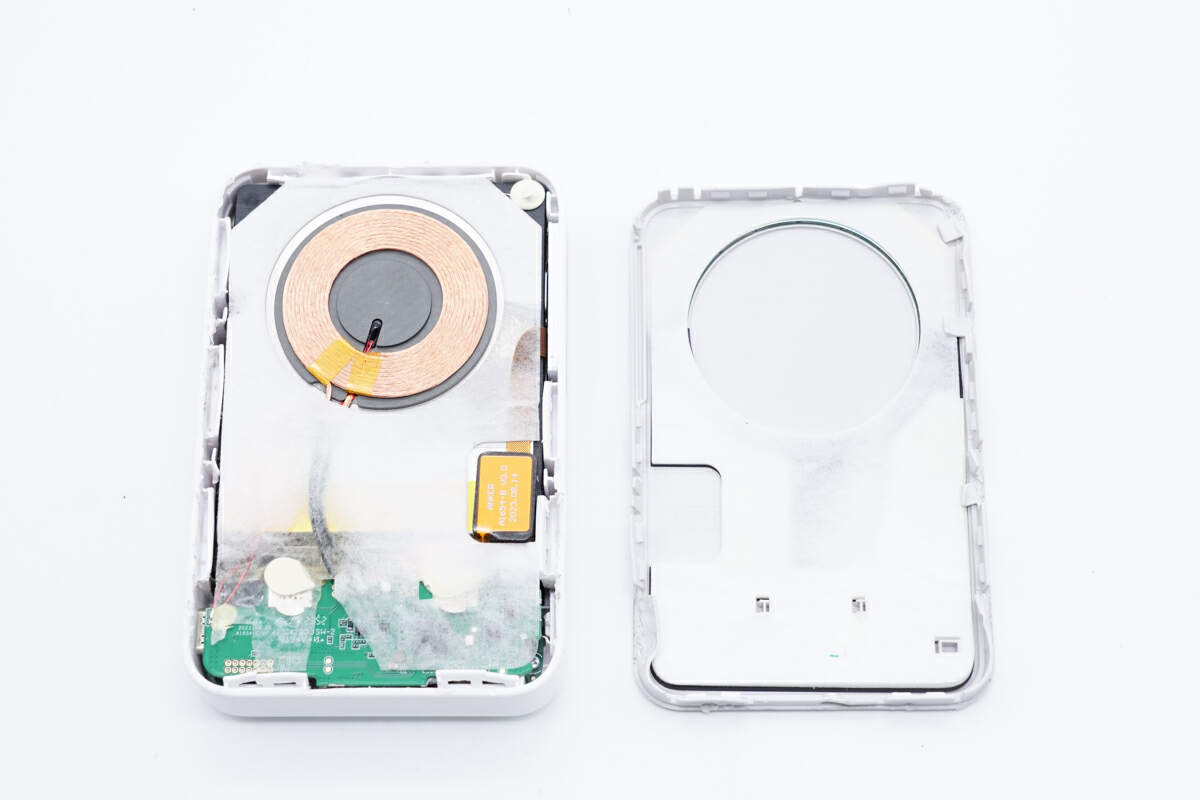
First, pry off the case along the gap.
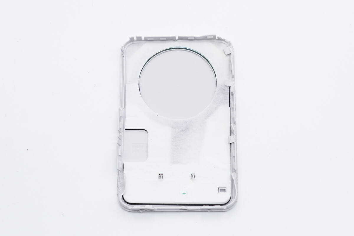
There are graphite thermal pads and aerogel inside the cover.
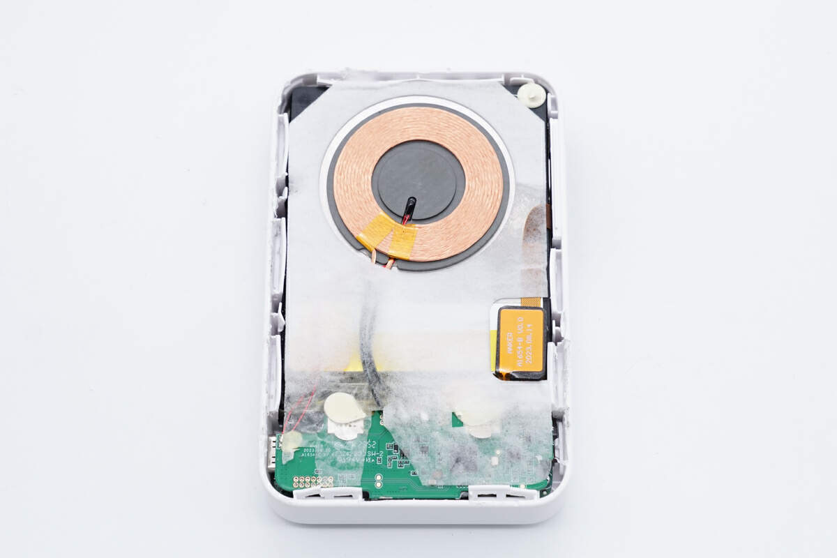
There is a wireless charging coil, touch detection pad, and PCBA module inside the case.
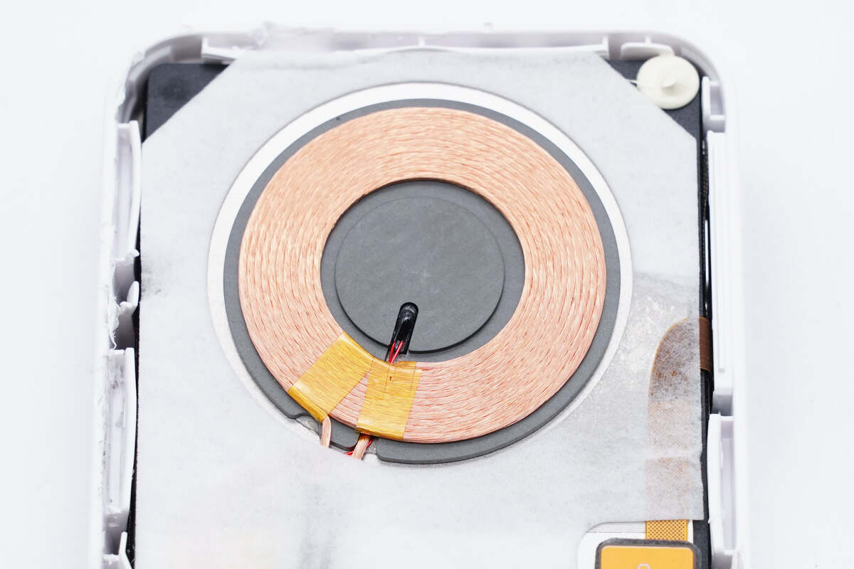
The wireless charging coil is wound with Litz wire and has a thermistor inside to detect the temperature.
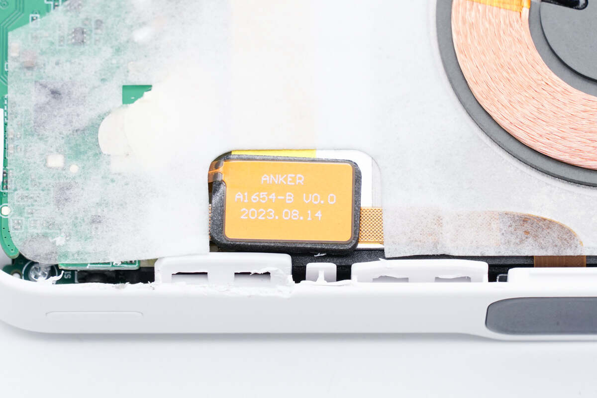
The touch detection pad is printed with ANKER, A1654-B. With the touch detection chip, wireless charging is automatically turned on when the power bank is attached to the phone.
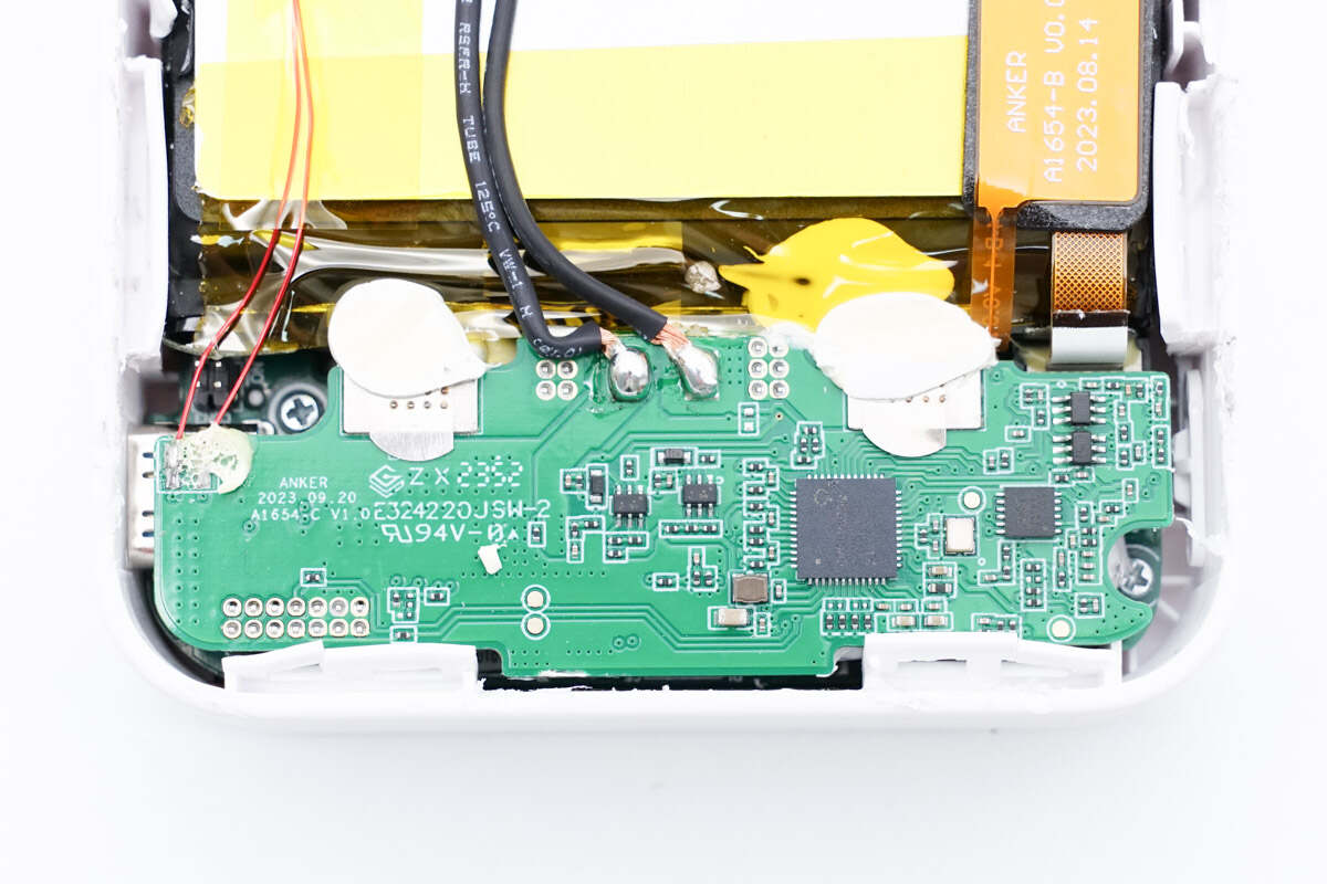
The NTC thermistor and wireless charging coil are connected to the PCBA module by soldering.
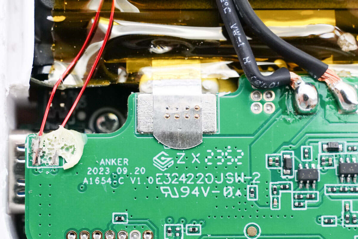
The battery is connected to the PCBA module by spot welding.
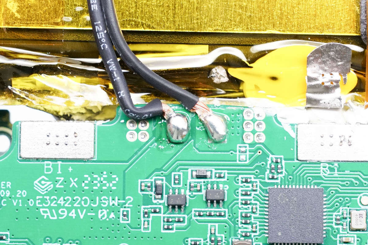
The welding points of the wireless charging coil are round and full.
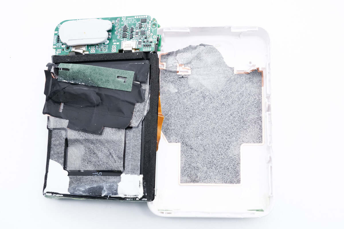
Take out the PCBA module and battery from the case. There is foam on the edge of the battery and a graphite thermal pad inside the case.
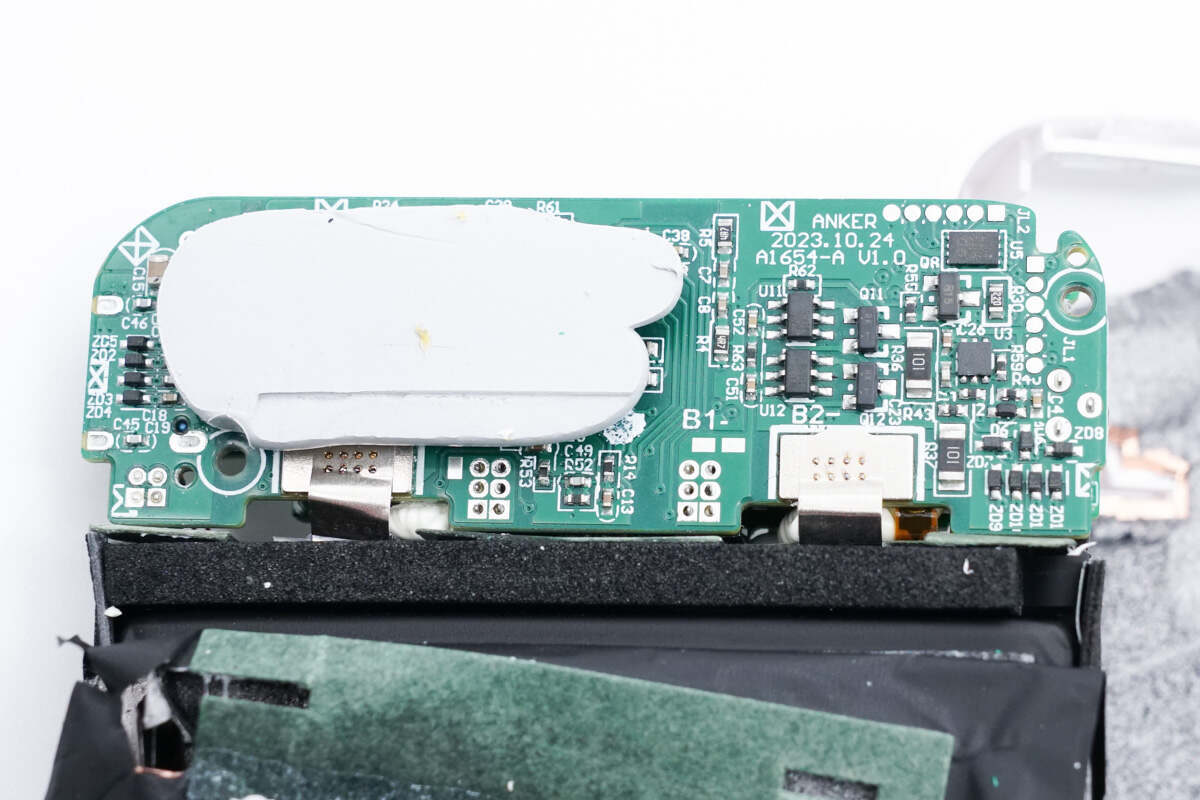
The PCBA module enhances heat dissipation through the potting compound.
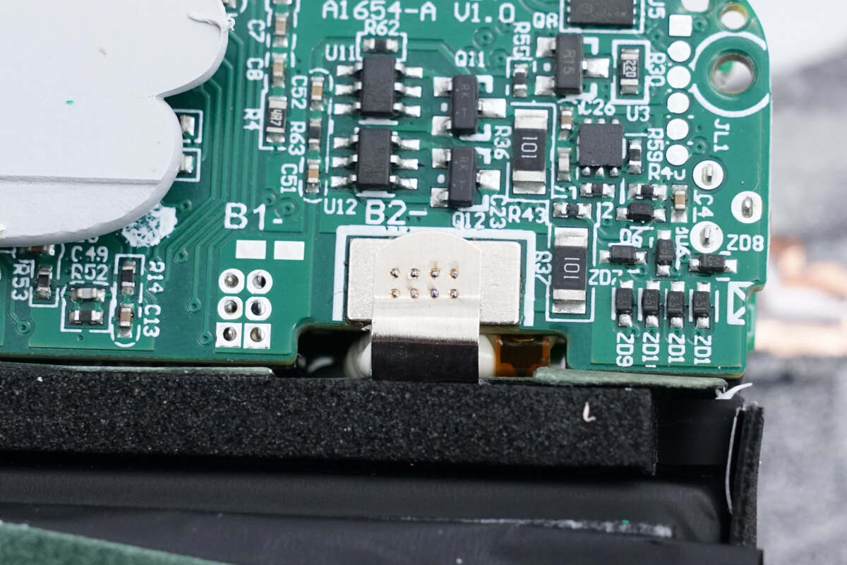
Another battery is also connected to the PCBA module by spot welding.
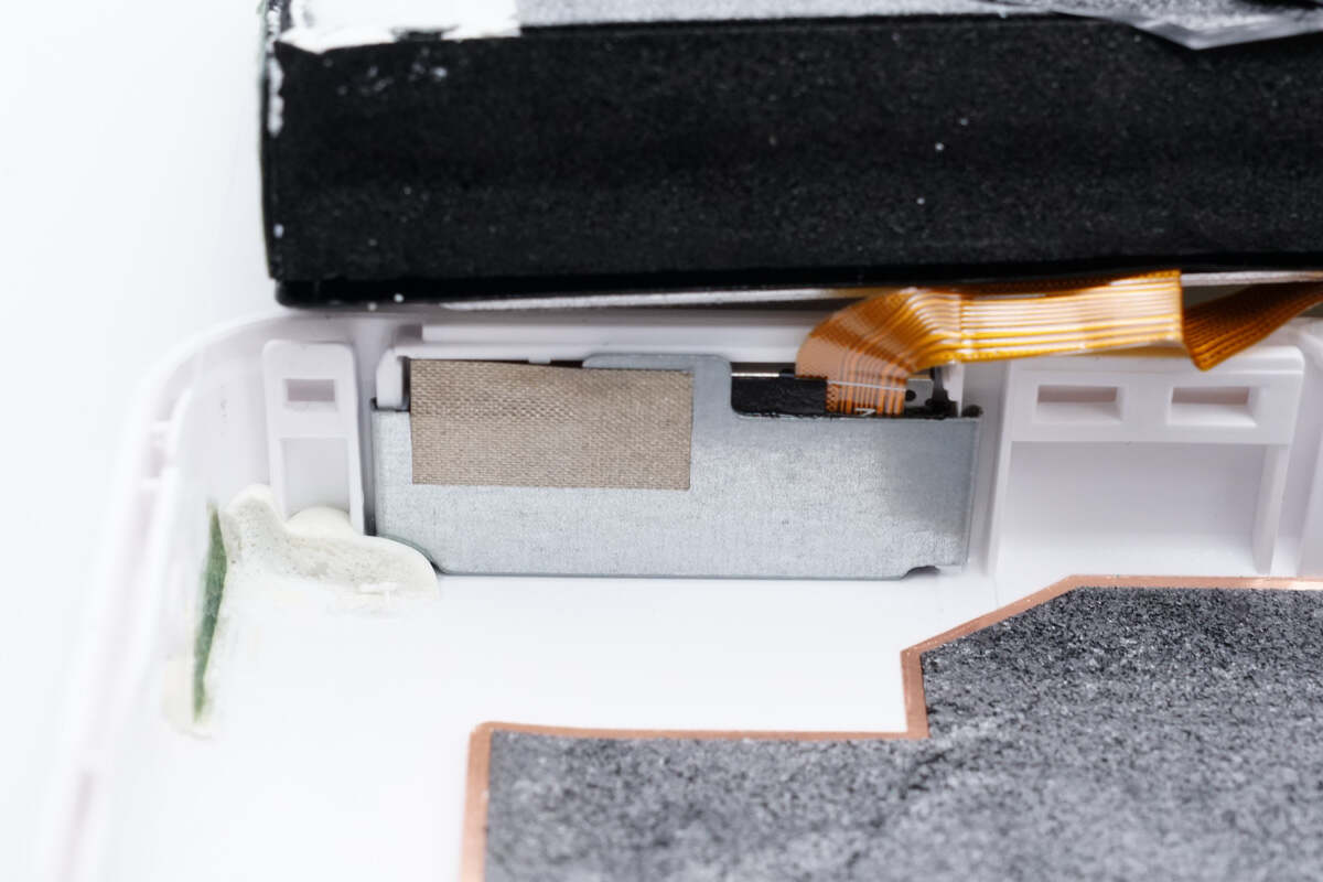
The LCD is fixed with a metal plate.
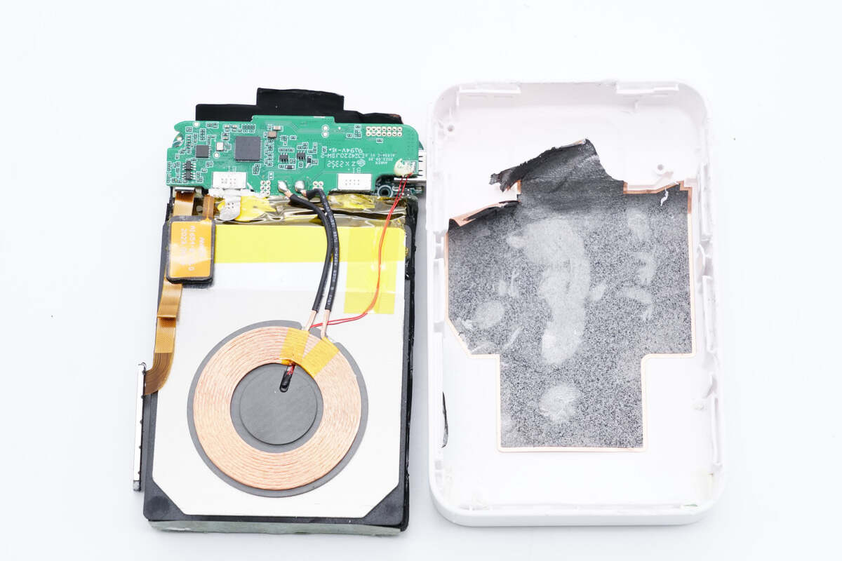
Remove the metal plate that fixes the LCD and separate the PCBA module from the casing.
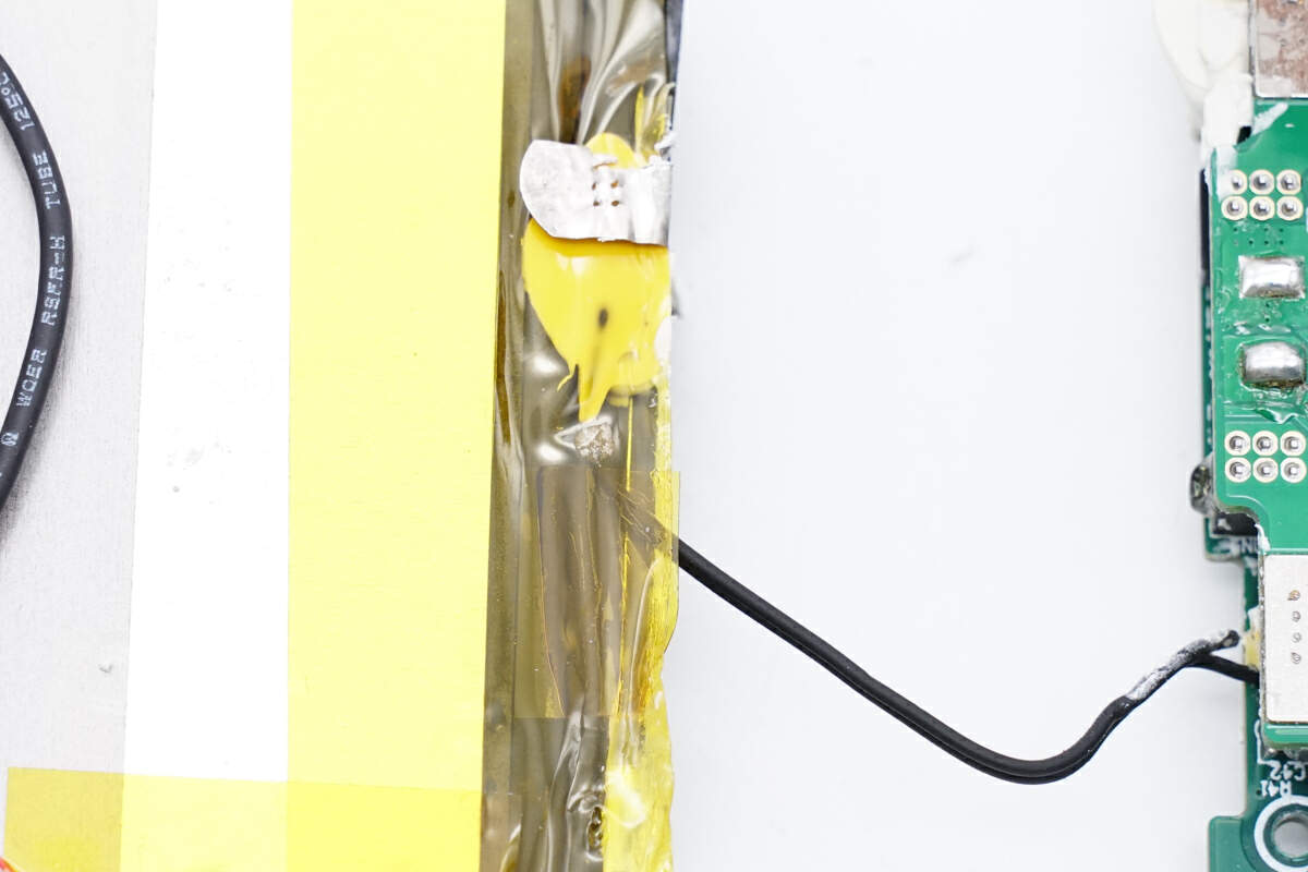
The battery pack is attached with a thermistor to detect the temperature.
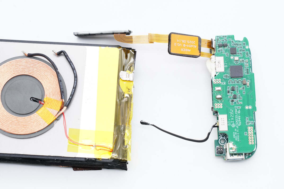
This is the thermistor used to detect the battery temperature.
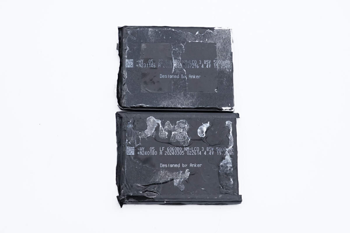
The battery pack uses two Lithium batteries connected in series.
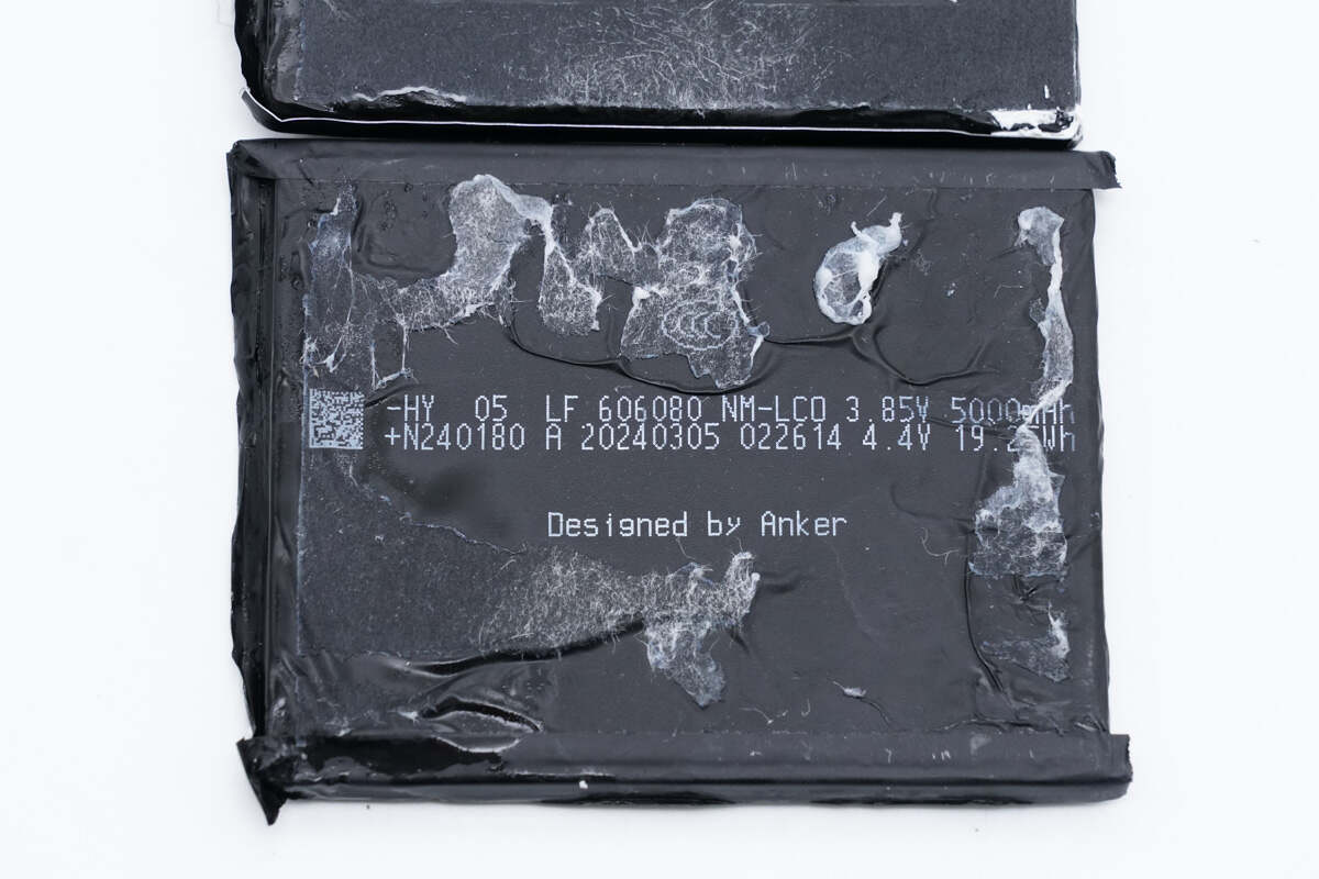
The 3.85V high voltage lithium-ion polymer battery has a size of 606080 and a battery capacity of 5000mAh. The input limit voltage is 4.4V, the energy is 19.25Wh, and it is designed by Anker.
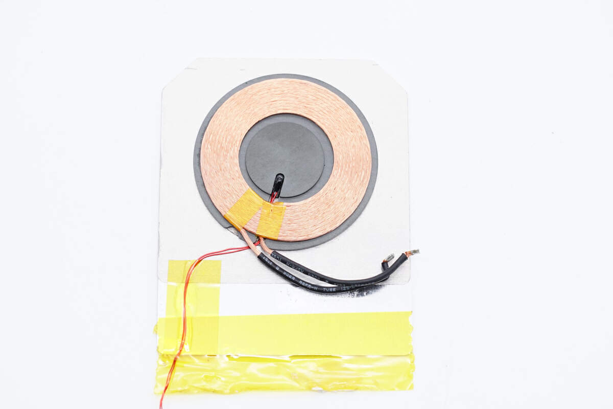
The wireless charging coil is glued to the aluminum plate.
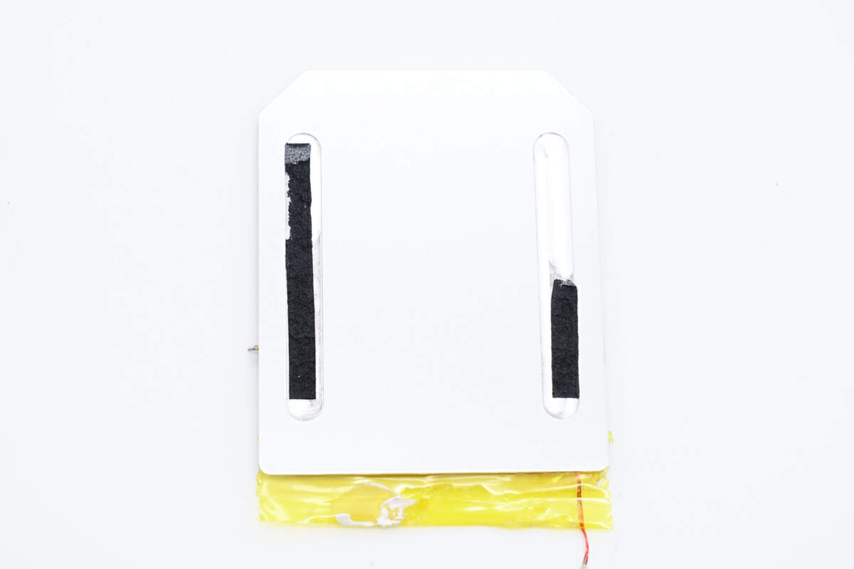
The back of the aluminum plate is fixed to the battery with double-sided tape.
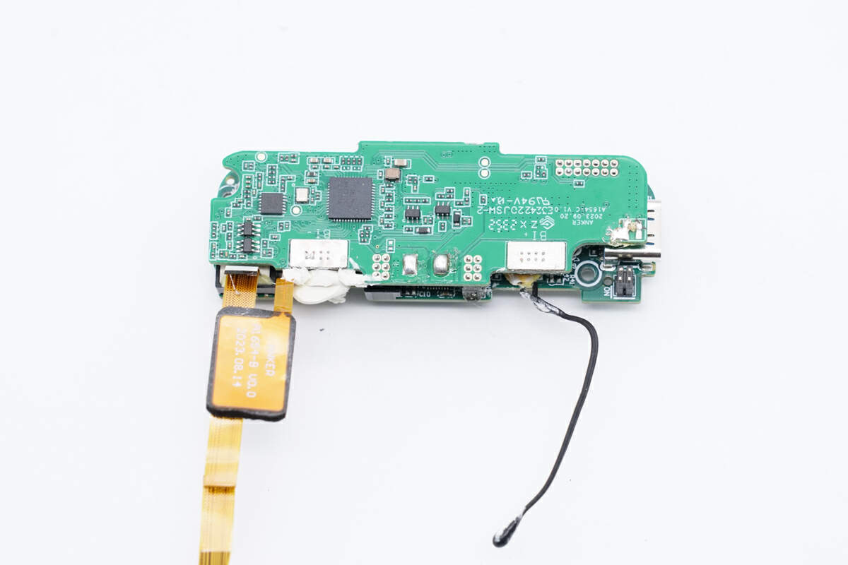
The upper PCBA module is a wireless charging module, which is welded with a wireless charging coil and an NTC thermistor.
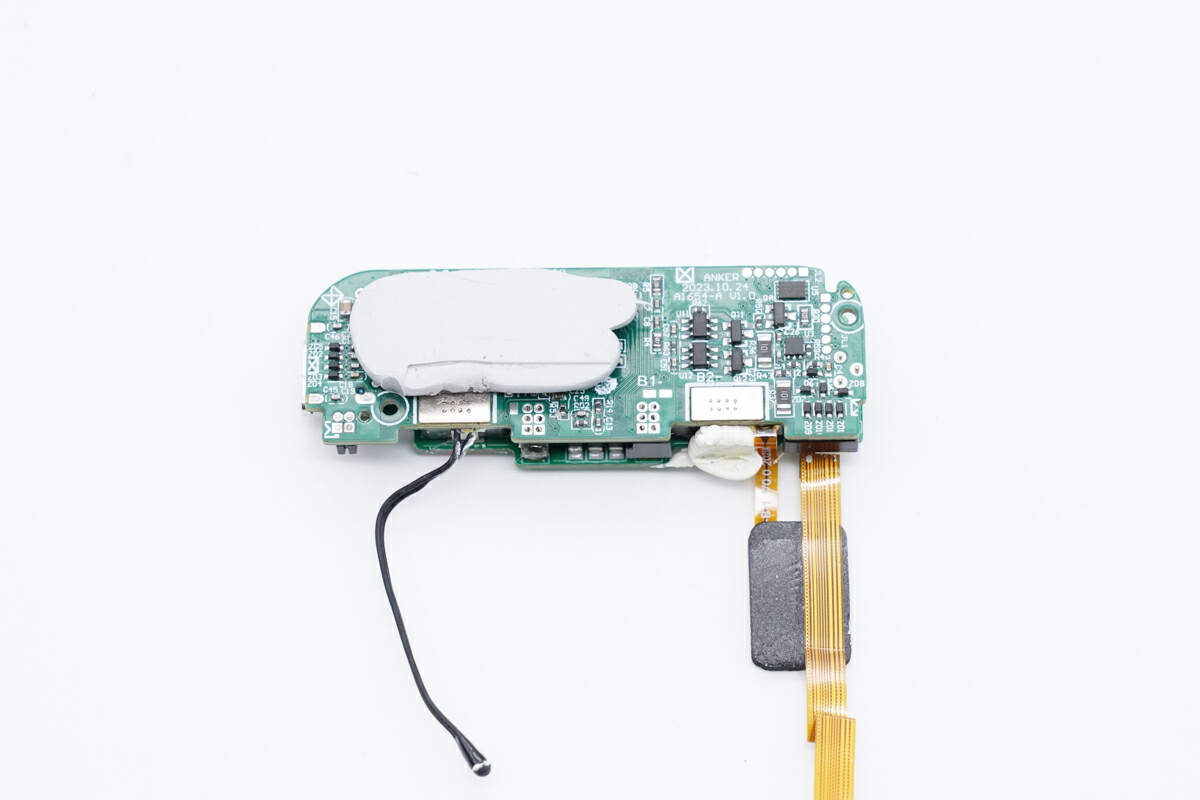
The bottom PCBA module enhances heat dissipation through the potting compound.
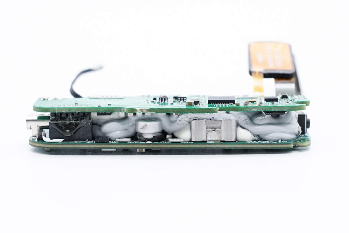
Filter capacitors and alloy inductors are arranged between the two layers of PCBA modules, the components are filled with potting compound, and the PCBA modules are connected through connectors.
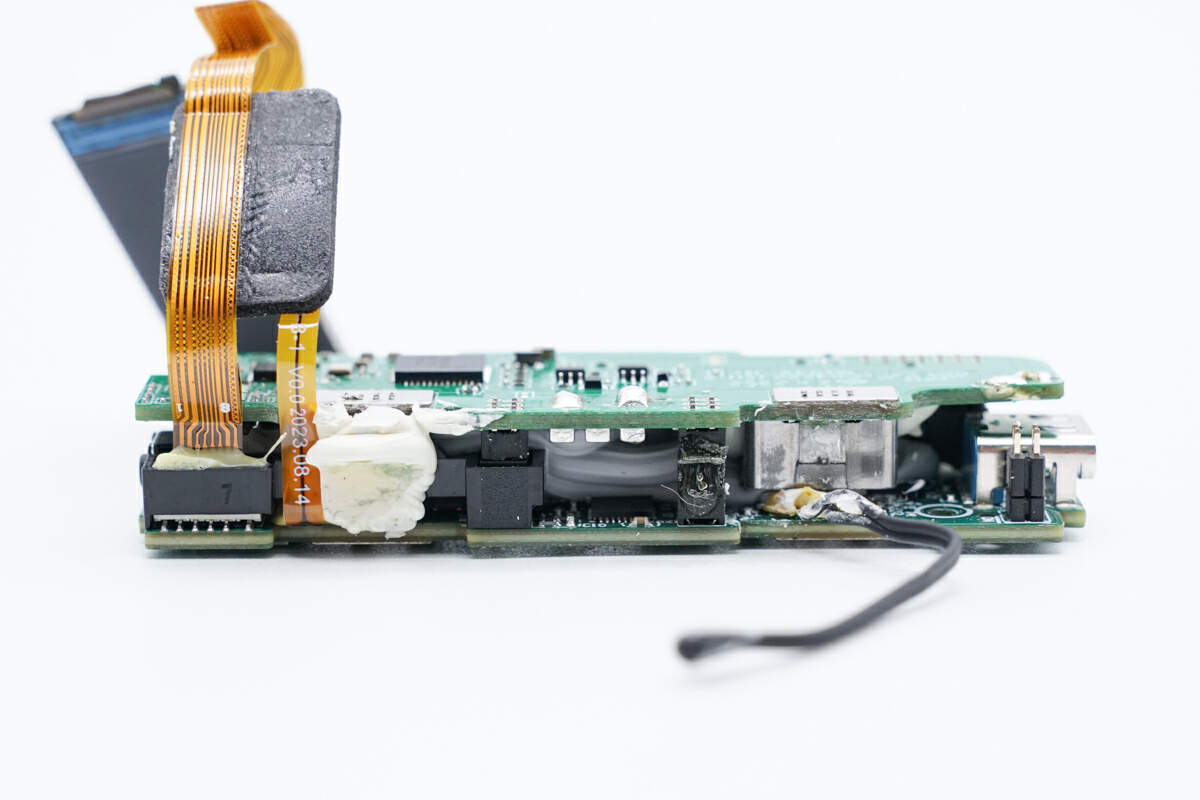
The other side has the display connector and touch detection pad, as well as the connector that connects the two layers of PCBA modules.
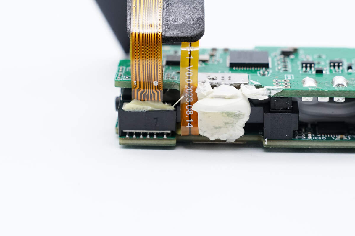
This is the LCD screen connector.
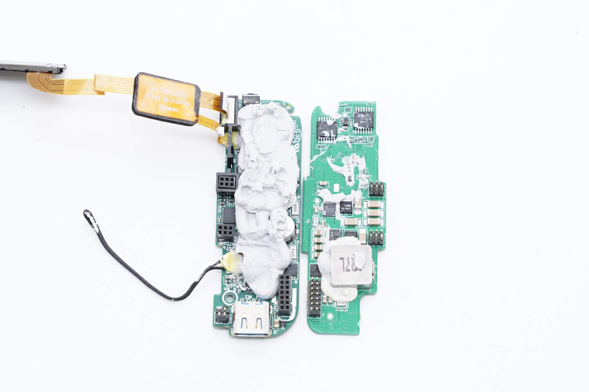
Separate two layers of the PCBA module. The inside is filled with potting compound to enhance heat dissipation.
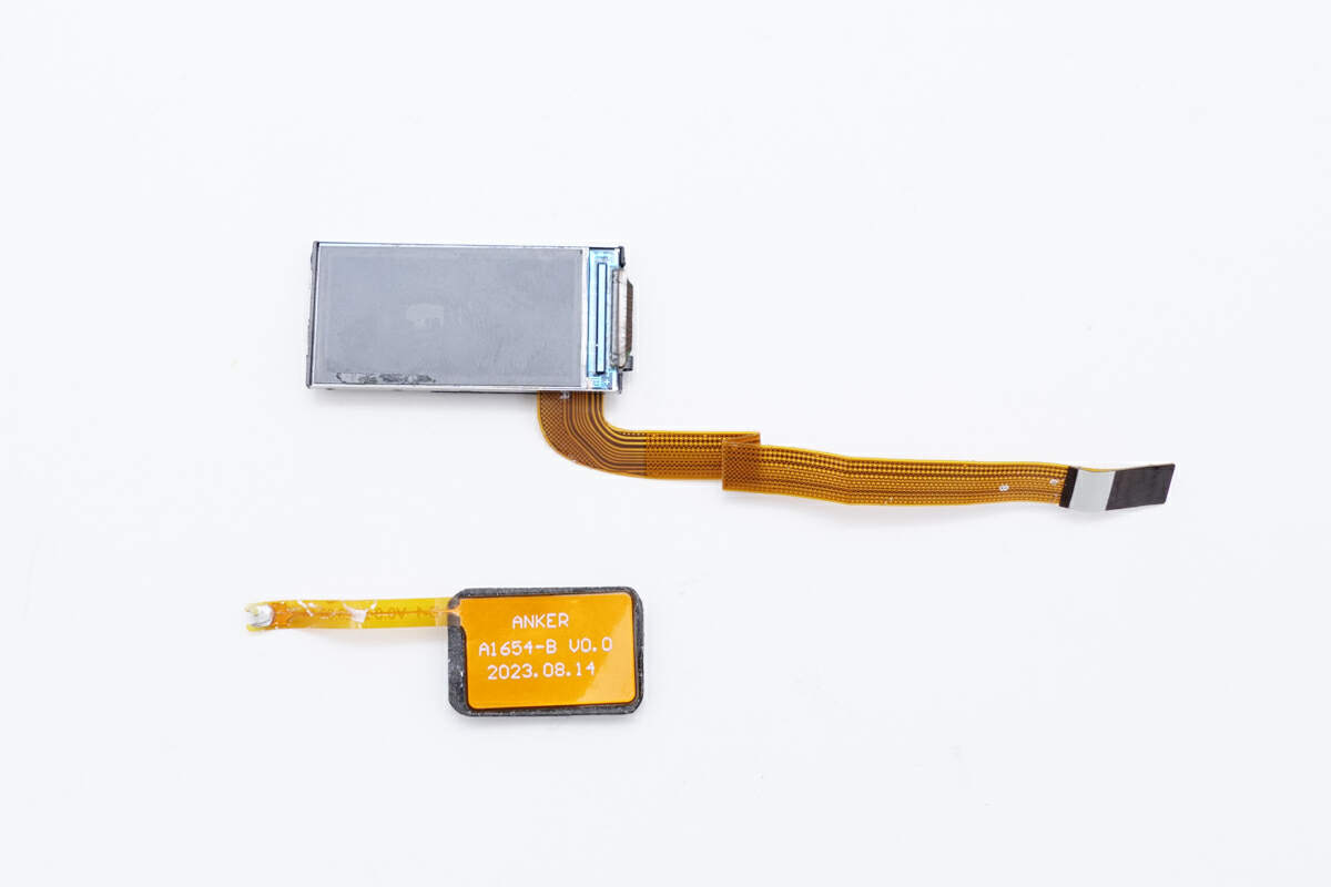
The LCD is connected via a flat cable, and the touch detection chip is connected by welding.
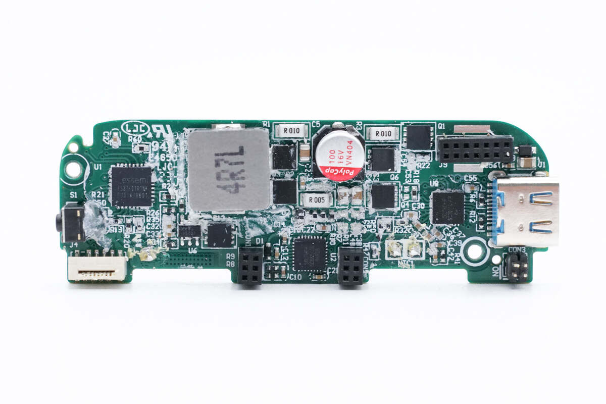
Clean up the PCBA module. The front of the bottom PCBA module is welded with micro-switch button, screen connector, MCU, alloy inductor, battery protection circuit, inductor, synchronous buck-boost MOSFET, capacitor for output filtering, synchronous buck-boost controller, protocol chip, VBUS MOSFET, and USB-C female socket.
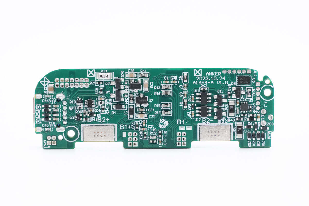
On the back, there are TVS diodes for interface electrostatic protection, battery balancing chips, touch detection chips, and memory.
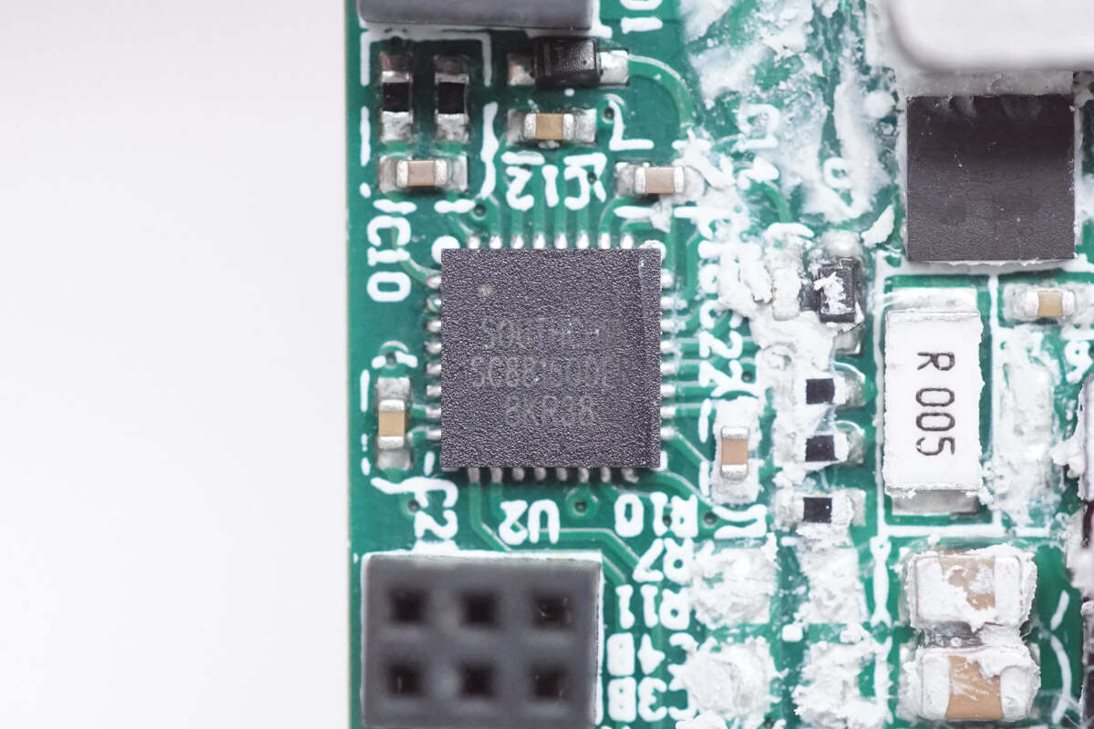
The buck-boost chip is from SouthChip and adopts QFN32 package. It is used for buck-boost voltage conversion, charging the battery, and the output of the USB-C port. It is a bidirectional synchronous buck-boost controller with an integrated I2C port, supporting 2.5 to 36V input and output voltage range, and supporting 1 to 6 battery strings. It has under-voltage protection, overvoltage protection, overcurrent protection, short-circuit protection, and thermal shutdown protection. Model is SC8815.
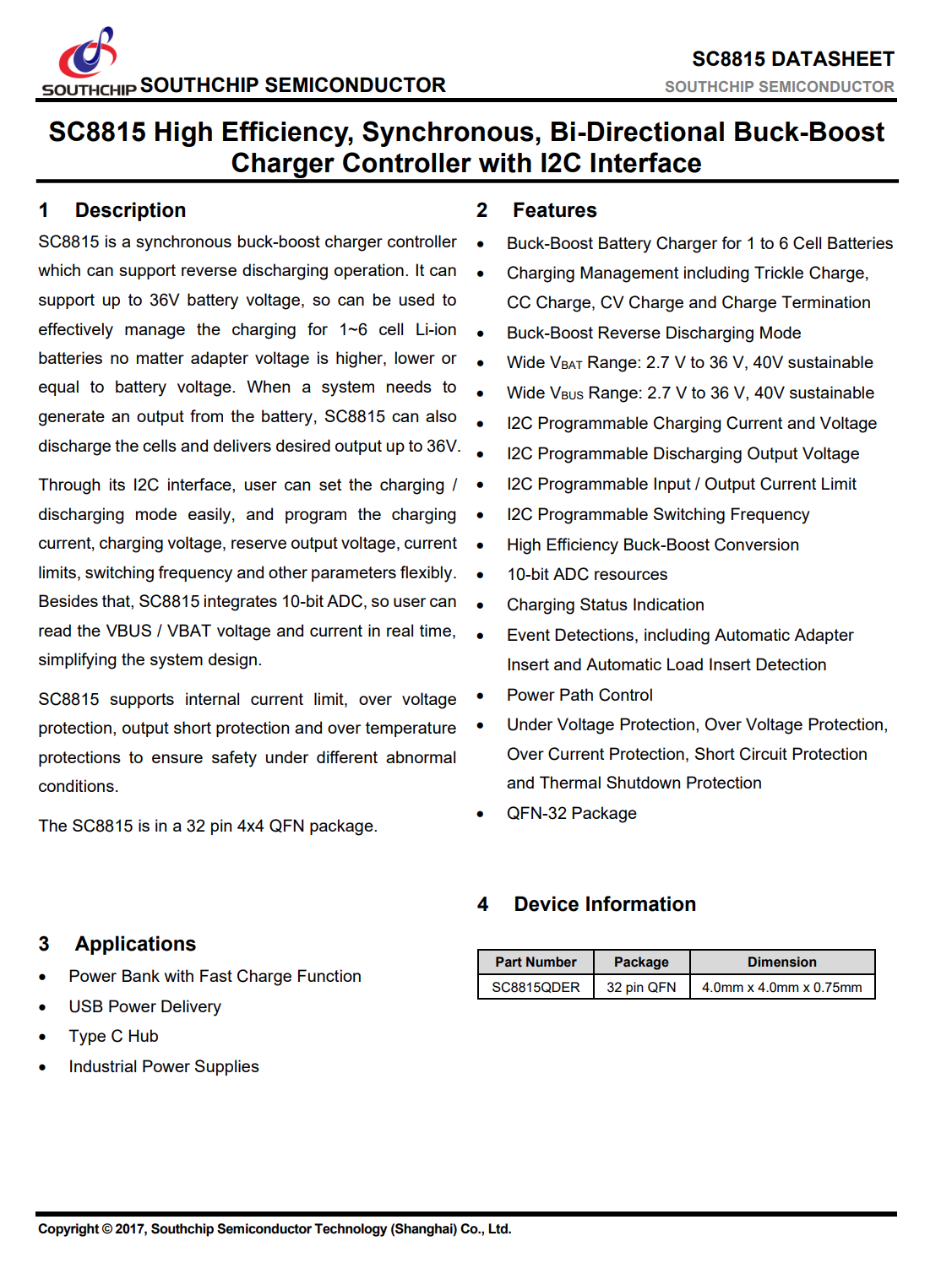
Here is the information about SouthChip SC8815.
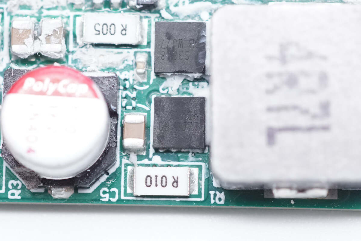
The synchronous buck-boost MOSFET is marked with S3818. Two of them form a full bridge.
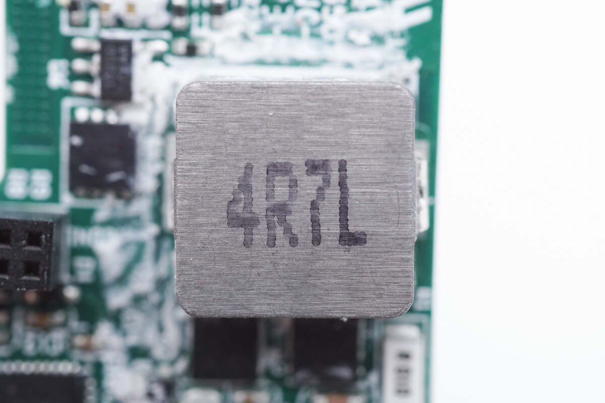
The alloy inductor adopts 10 x 10 mm package. 4.7μH.
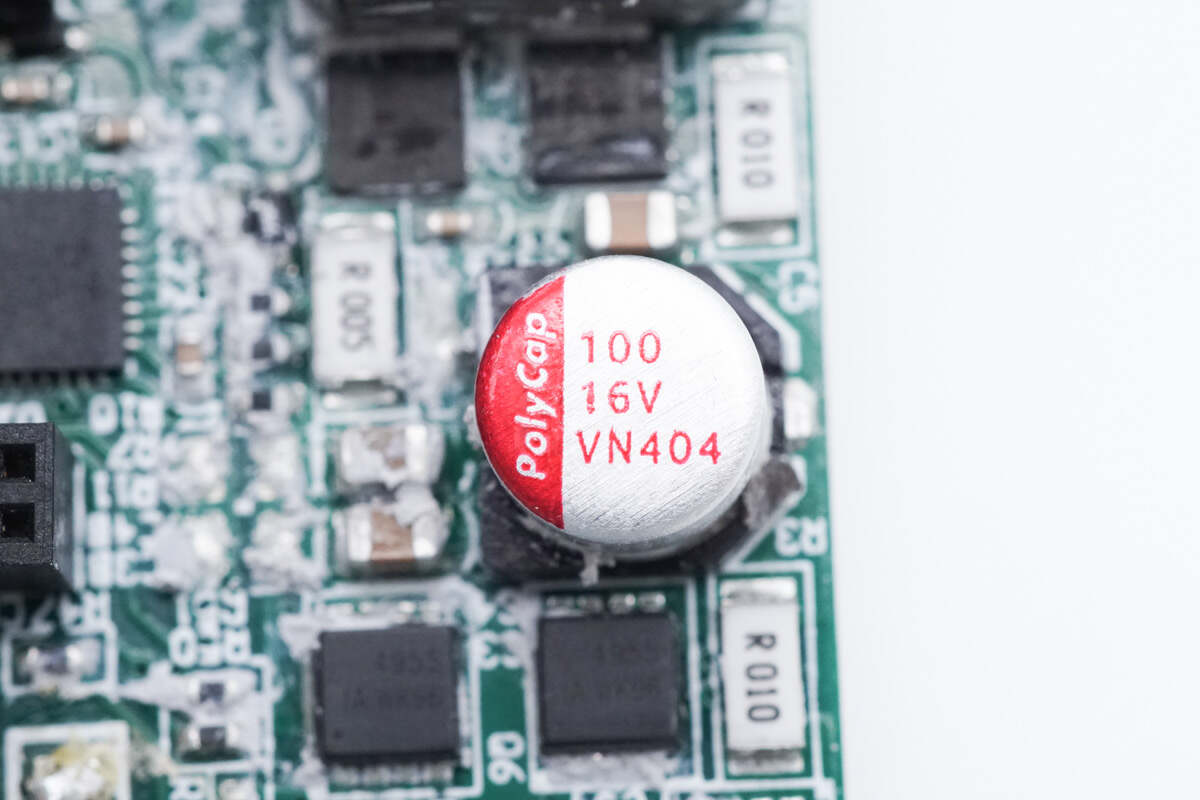
The filter capacitor is from PolyCap VN series. Heat resistant 105℃, 100μF 16V.
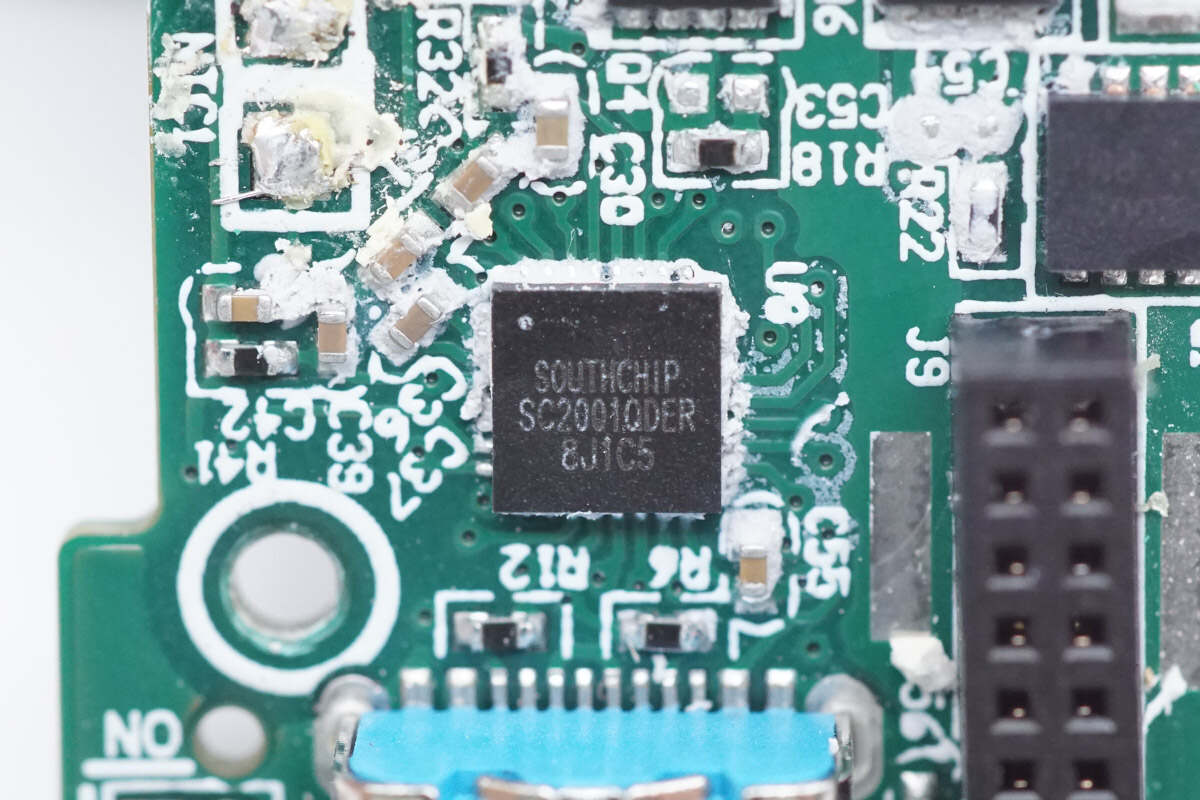
The protocol chip is from SouthChip and adopts QFN-32 package. It is a highly integrated USB PD controller that complies with the latest USB Type-C and USB PD standards. It has a 30V rated voltage and multiple built-in protections, including over-temperature protection, constant power, constant current, and over-voltage protection, to ensure the safe operation of the system. It integrates an MCU subsystem and supports programming through CC pins, a driver, a 10-bit ADC, and a high-precision amplifier, which can reduce the number of external components to a minimum. Model is SC2001.
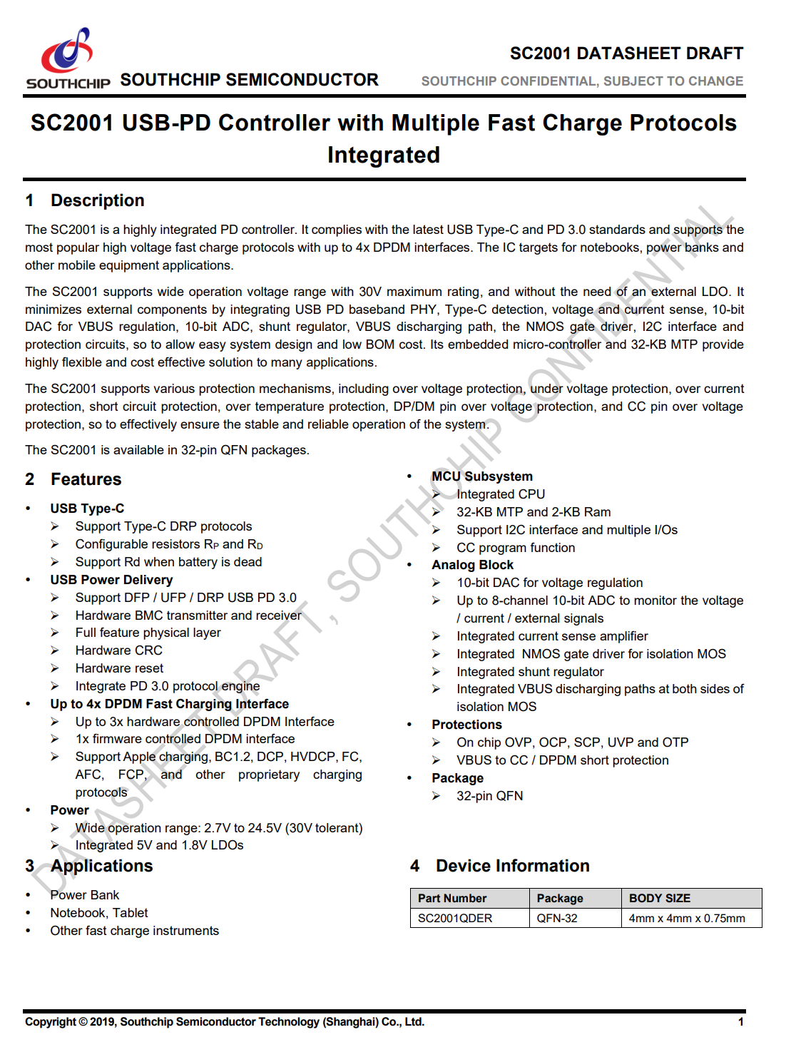
Here is the information about SouthChip SC2001.
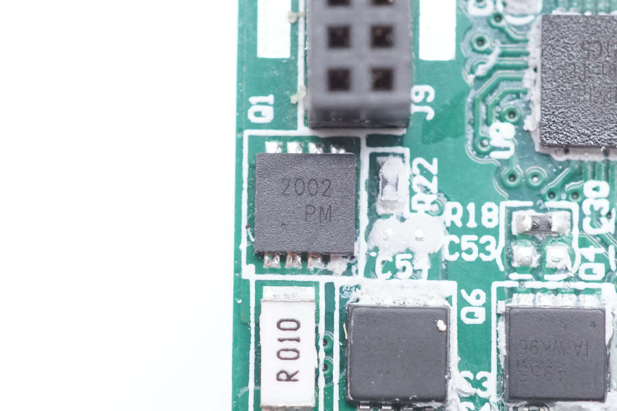
The VBUS MOSFET used to control the USB-C port output is marked with 2002.
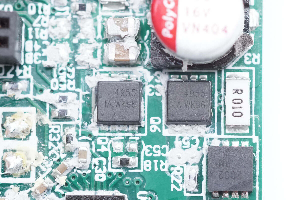
The other two VBUS MOSFETs are marked with 4955.
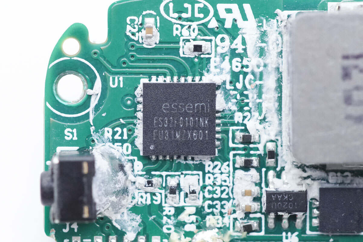
The MCU used to drive the display is from essemi and adopts QFN32 package. It is an ARM Cortex-M0 core with a main frequency of 52MHz. It integrates 64KB FLASH and 4KB SRAM and has a built-in 12-bit ADC, two I2C ports, one SPI port, and two USART ports. Model is ES32F0101NK.
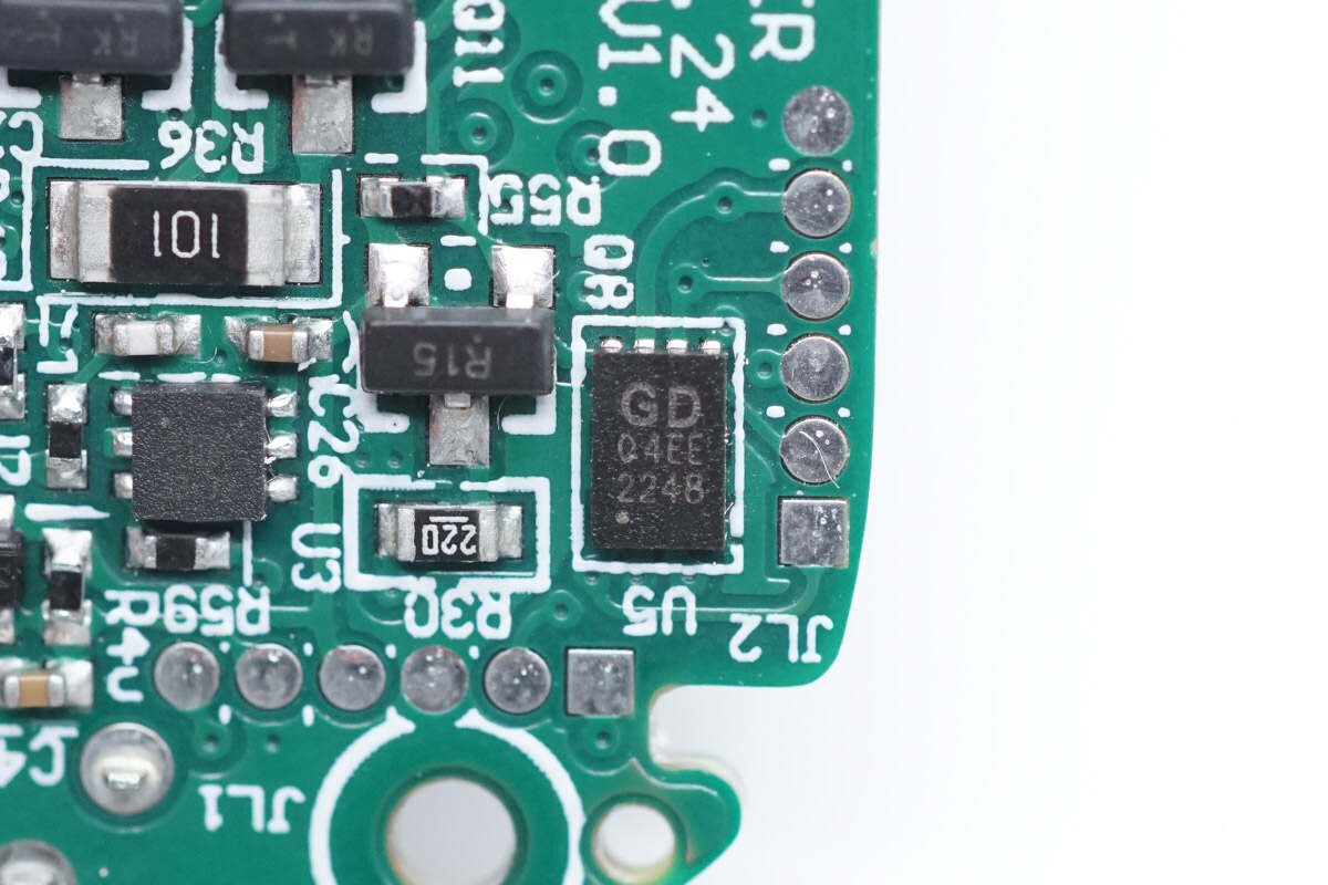
The memory marked with Q4EE is from GigaDevice and adopts USON8 package. Model is GD25Q80EEIG.
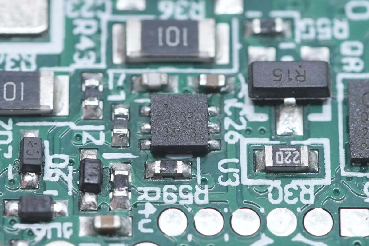
The touch detection chip marked with 31BP is from HYNITRON. It adopts DFN2*2-6 package. It can be configured into multiple modes through pins. Model is HK31BP.
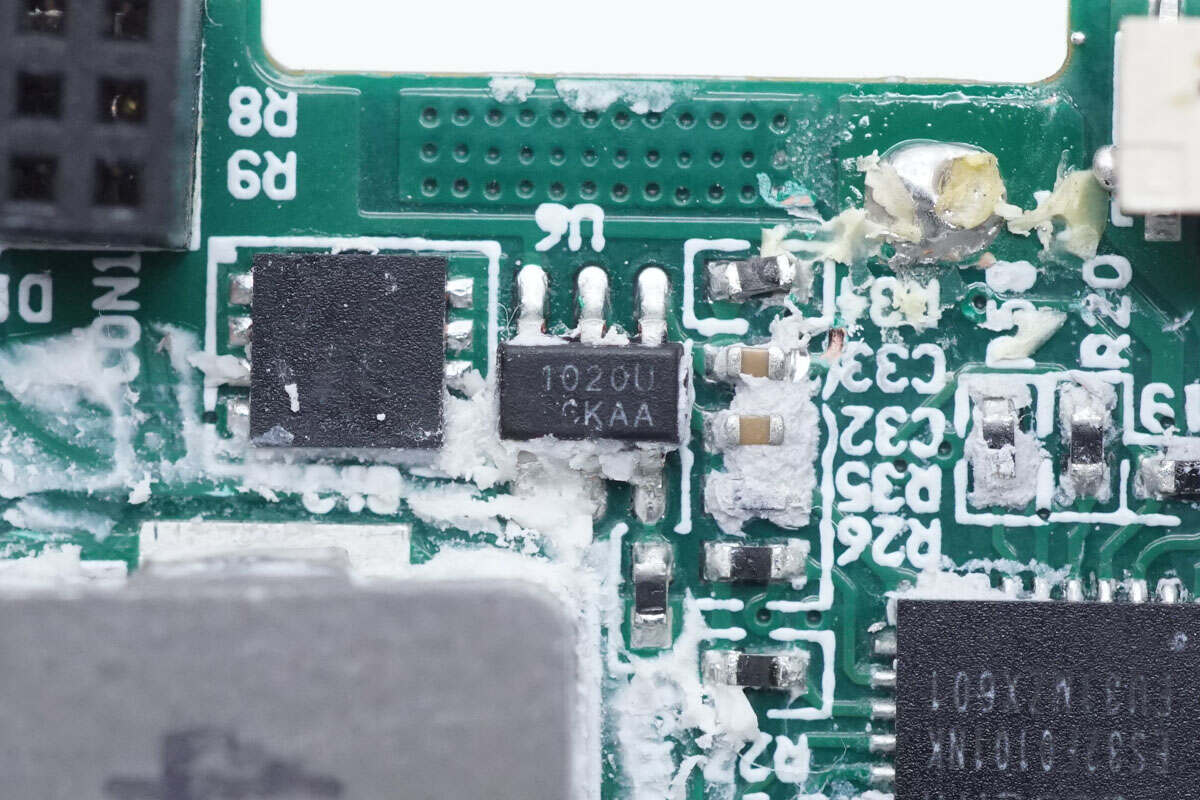
The battery protection chip marked with 1020U is from iCM. It adopts SOT23-6 package. It has a built-in high-precision voltage detection circuit and current detection circuit, and the overcharge protection voltage is 4.37V, with 25mV accuracy. It supports the detection of overcharge, over-discharge, discharge overcurrent, short circuit, and charge overcurrent. Model is CM1020-UC.
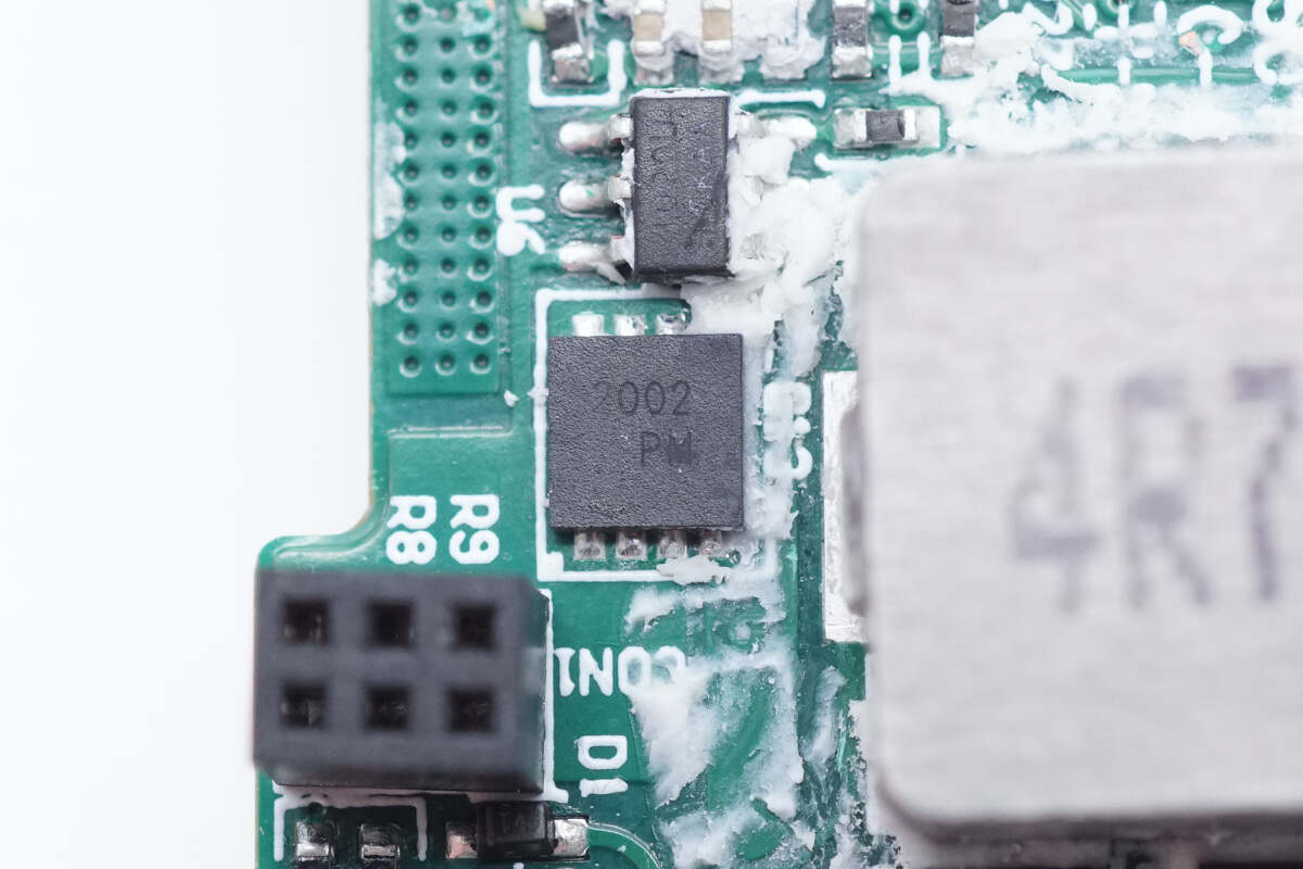
The battery protection MOSFET is marked with 2002.
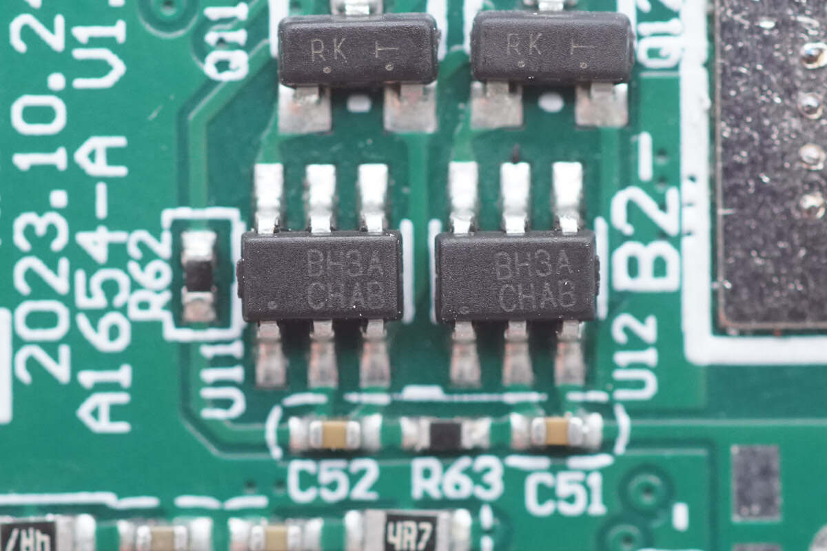
The two battery balancing chips marked with BH3A are from iCM. They adopt SOT23-6 package. It integrates a high-precision voltage detection circuit and delay circuit and realizes battery pack balancing by detecting the battery voltage. Model is CM1010-H.
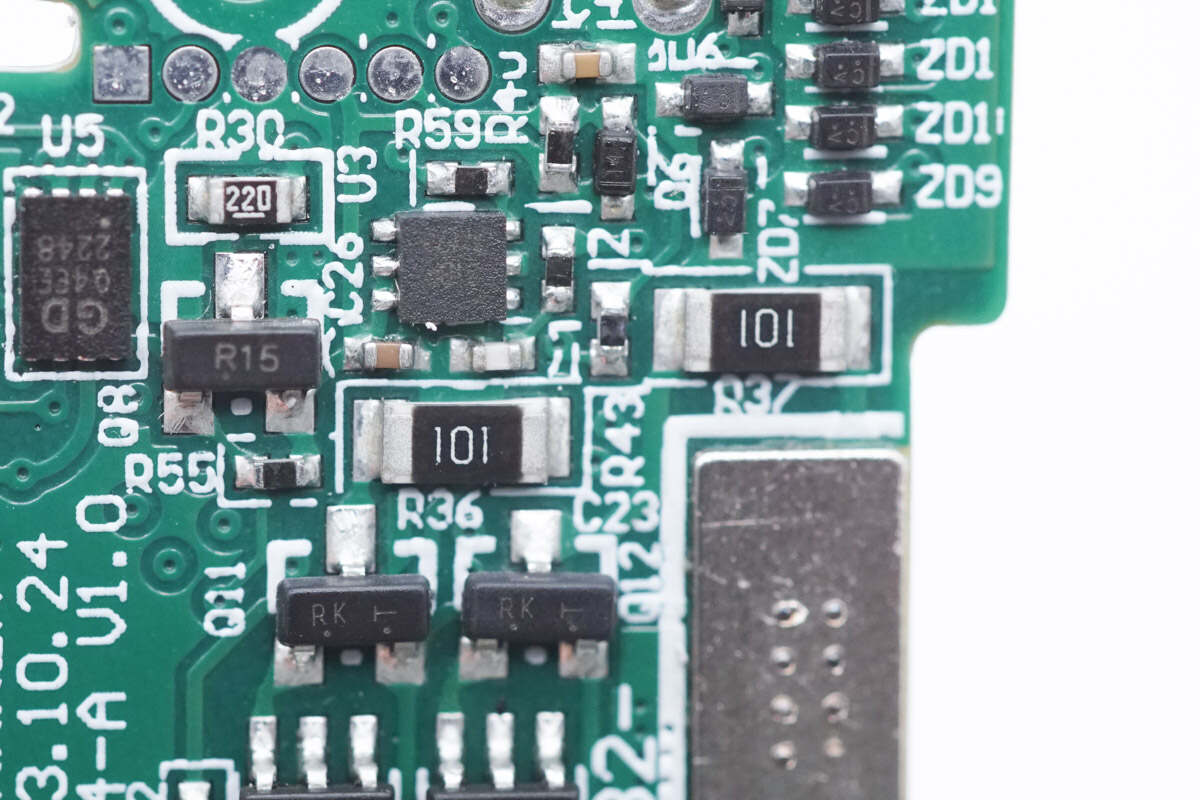
This is the external balancing MOSFETs and balancing resistors.
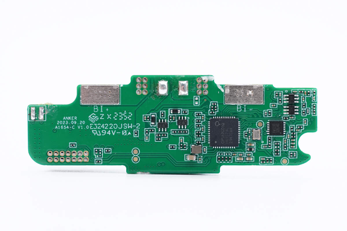
The wireless charging master control chip and secured encryption chip are installed on the front of the upper PCBA module.
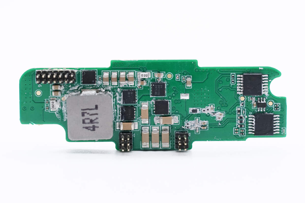
On the back are alloy inductors, boost MOSFETs, filter capacitors, MOSFETs for switching resonant capacitors, and two quad op-amps.
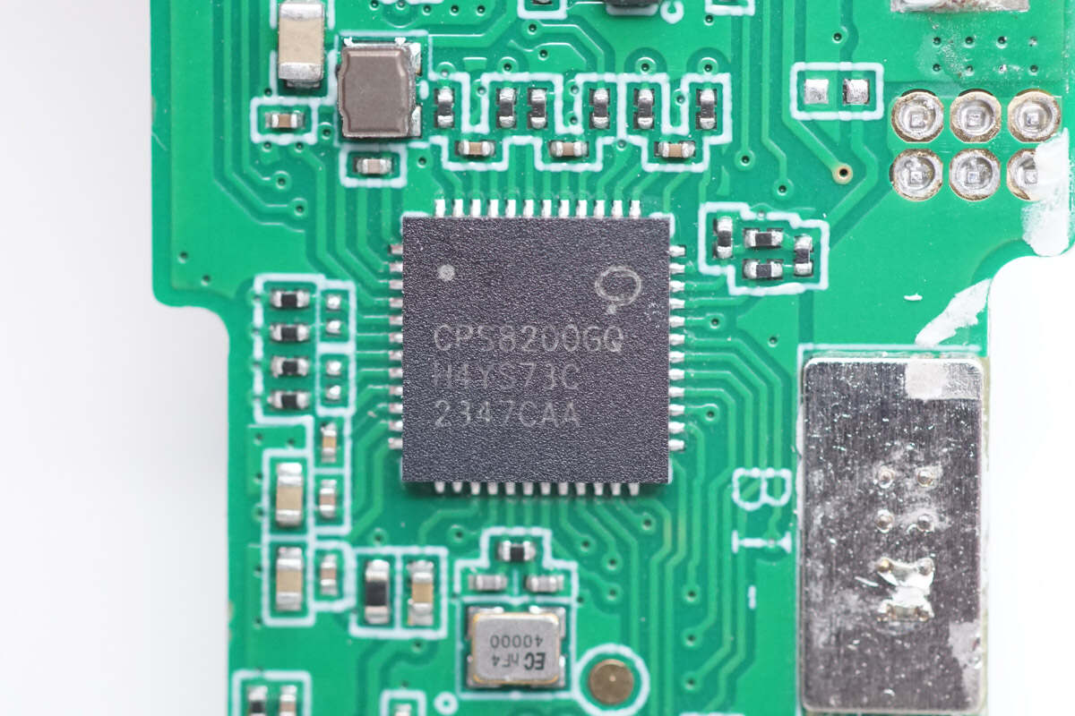
The wireless charging master control chip is from CPS. It has an integrated 32-bit processor, built-in 64+2KB MTP, 32KB ROM and 2KB SRAM. It supports programming via CC and DPDN. It has two I2C ports and two UART ports. It supports QC2.0/QC3.0/PD3.1/SCP/AFC fast charging protocols. Model is CPS8200.
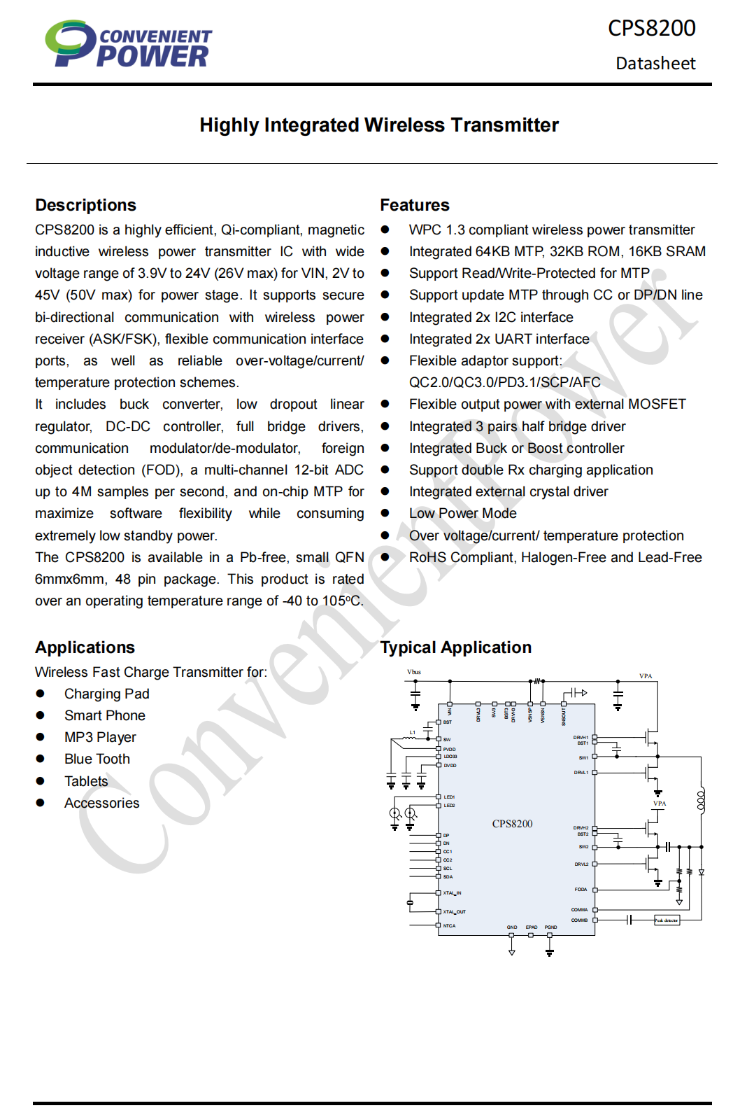
Here is the information about CPS CPS8200.
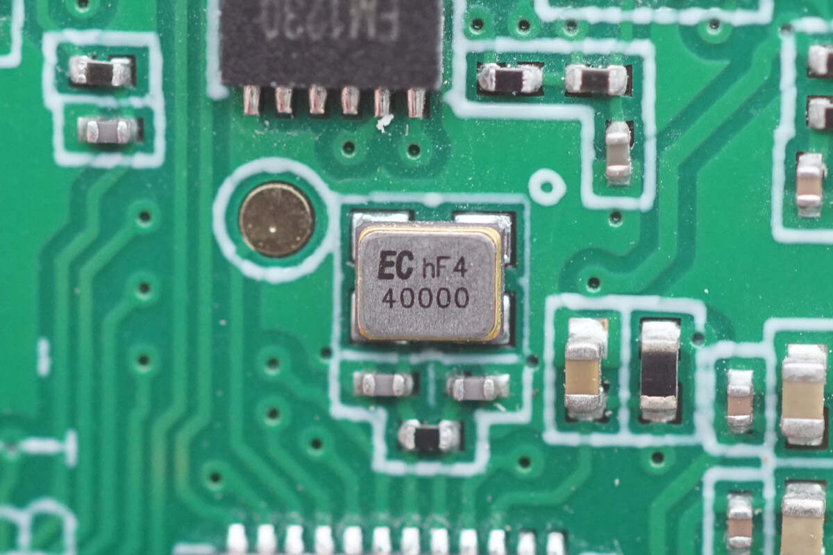
This is a passive clock crystal. 40.000Mhz.
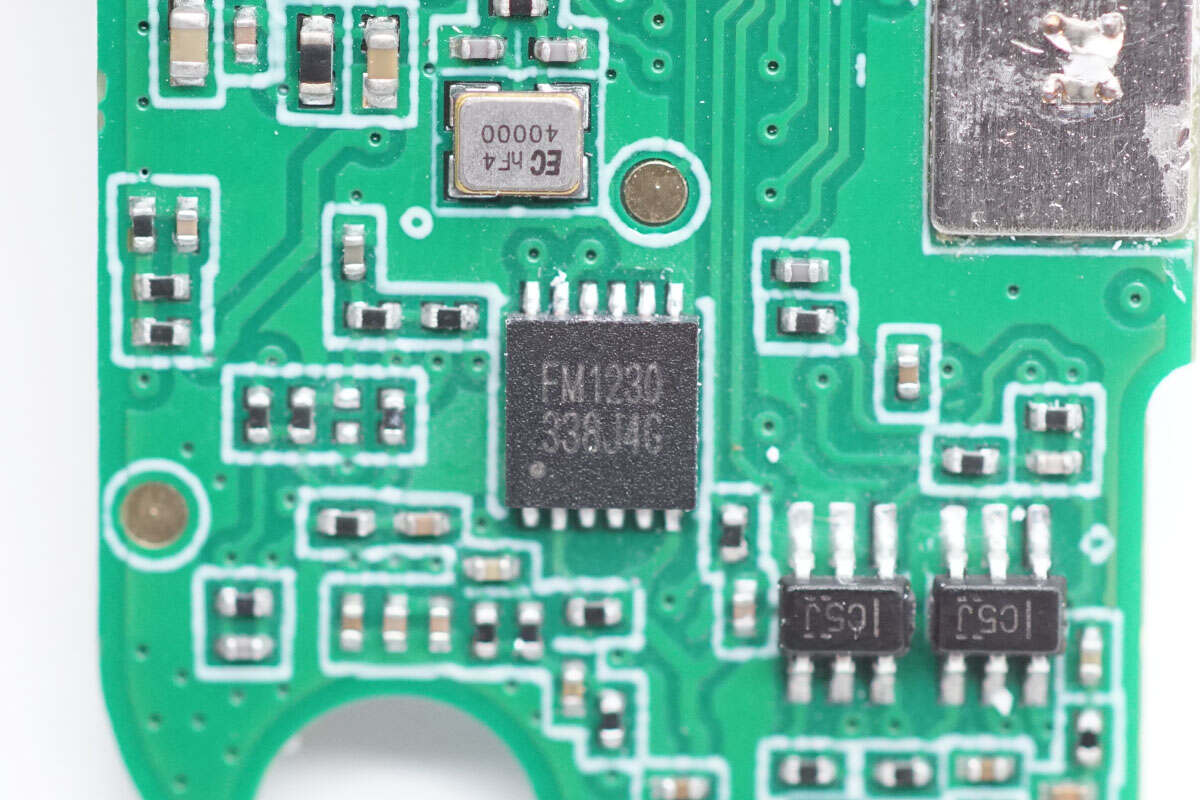
The secured encryption chip is from FUDAN. It supports DES/TDES, AES, SM4 symmetric algorithms, RSA, ECC, SM2 asymmetric algorithms, SHA1, SHA224, SHA256, SM3 hash algorithms, and other security algorithms. It has multiple protection capabilities, supporting symmetric and asymmetric encryption and decryption operations, secure storage, identity authentication, and other functions. Model is FM1230.
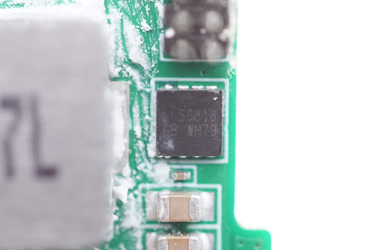
The boost MOSFET is marked with S3818. Same as synchronous buck-boost MOSFET.
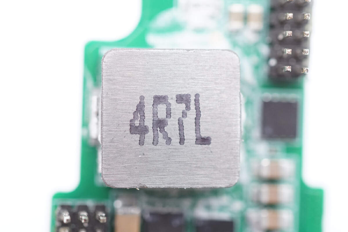
This is an alloy inductor. 4.7μH.
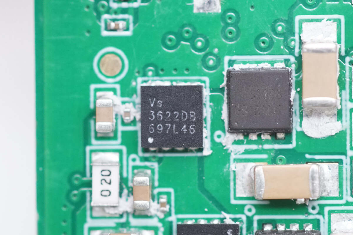
The wireless charging power MOSFET is from Vergiga and adopts DFN3*3 package. The dual NMOS is connected via a half-bridge, with a withstand voltage of 30V and a conduction resistance of 8.2mΩ and 6mΩ respectively. Model is VS3622DB.
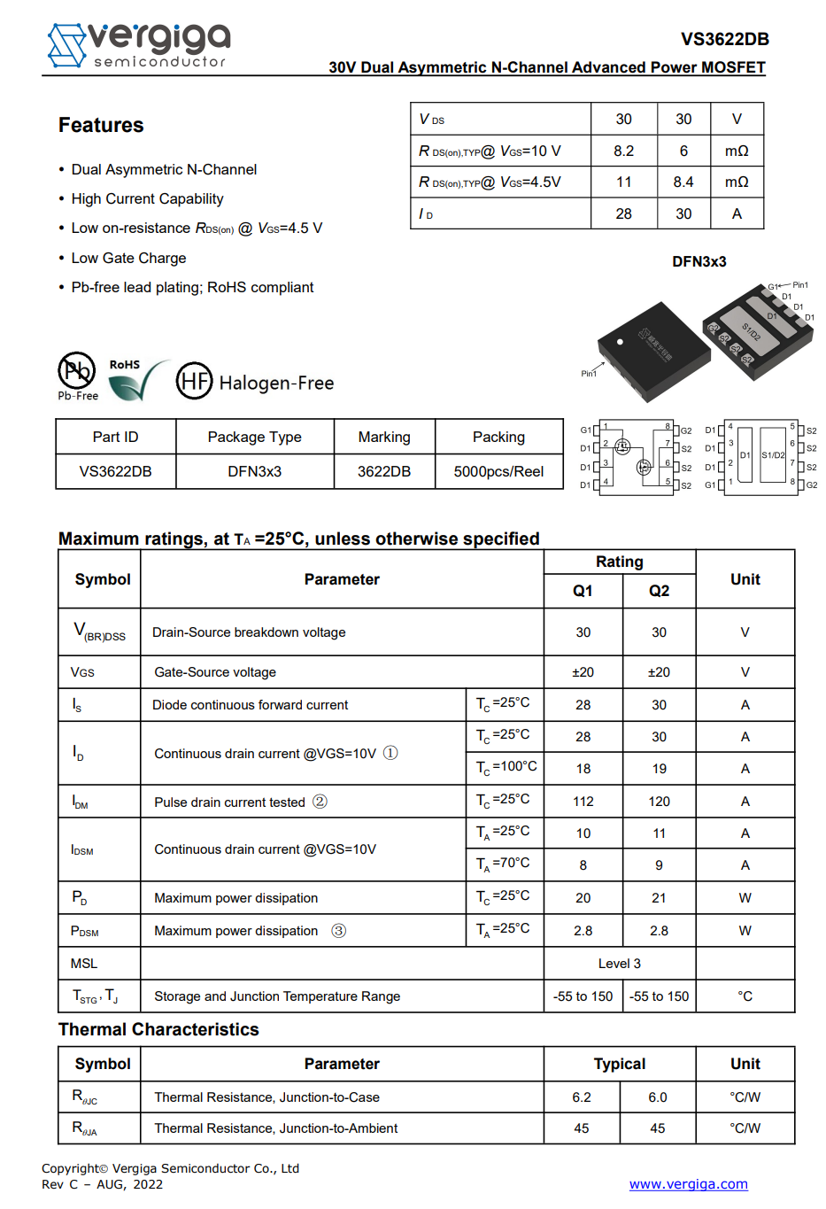
Here is the information about Vergiga VS3622DB.
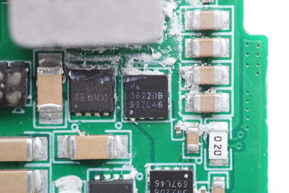
This is another Vergiga VS3622DB, two of them form an H-bridge for wireless charging coil driving.
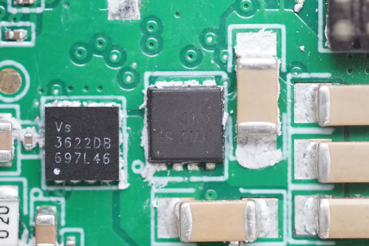
The MOSFET used to switch the resonant capacitor is marked with S1008.
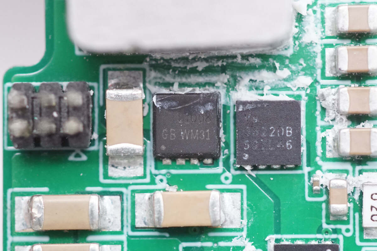
Another MOSFET that switches the resonant capacitor is also marked with S1008.
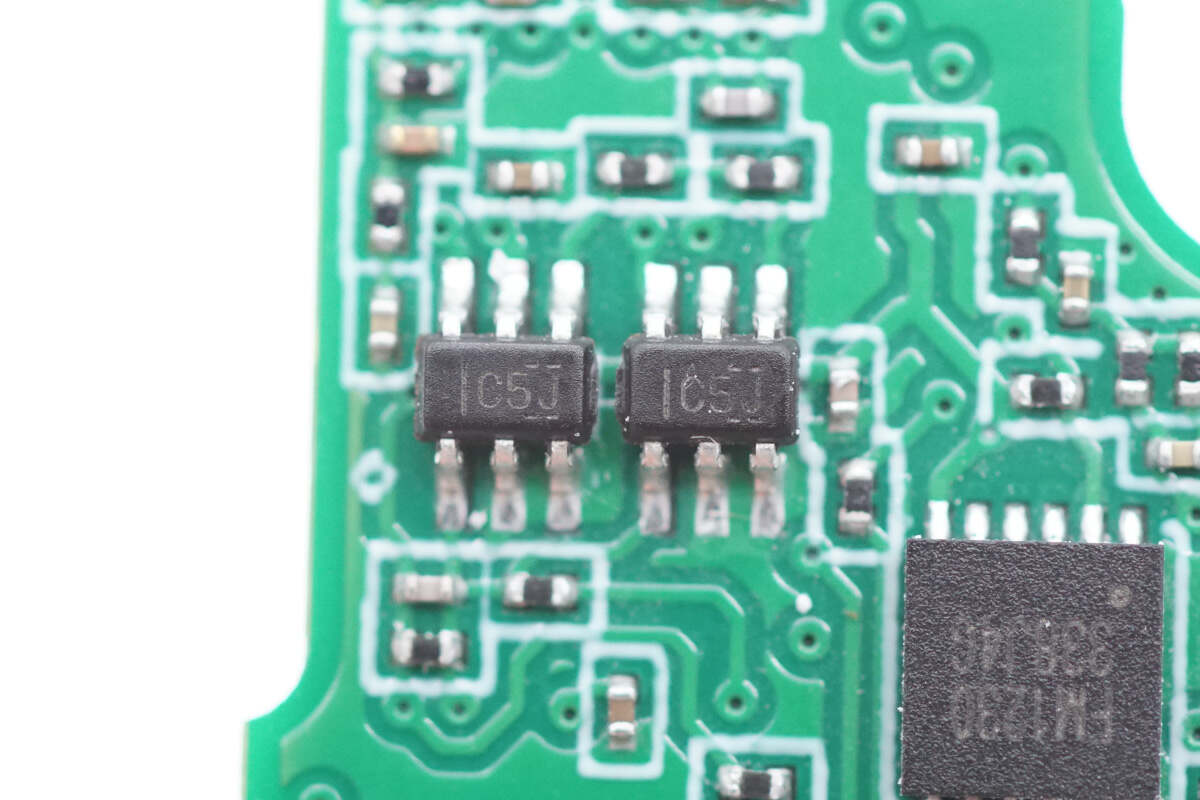
The analog switch IC is from TI and adopts SC70 package. Model is SN74LVC1G3157.
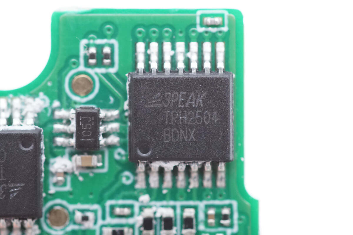
The quad op-amp is from 3PEAK and adopts TSSOP14 package. It has a 100mA high output current capability and supports rail-to-rail input and output. Model is TPH2504.
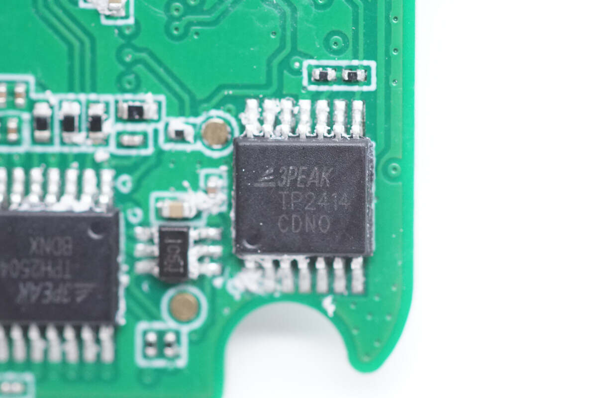
Another quad op-amp is also from 3PEAK and adopts TSSOP14 package. It has an output current of 70mA. Model is TP2414.
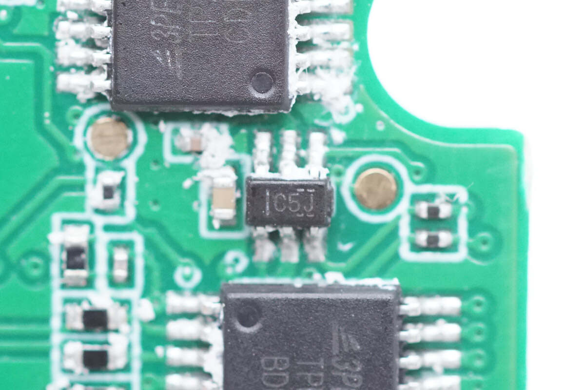
The Analog Switch IC between the two op amps is from TI. Model is SN74LVC1G3157.
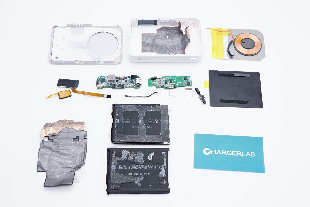
Well, those are all components of the Anker MagGo Magnetic Power Bank.
Summary of ChargerLAB
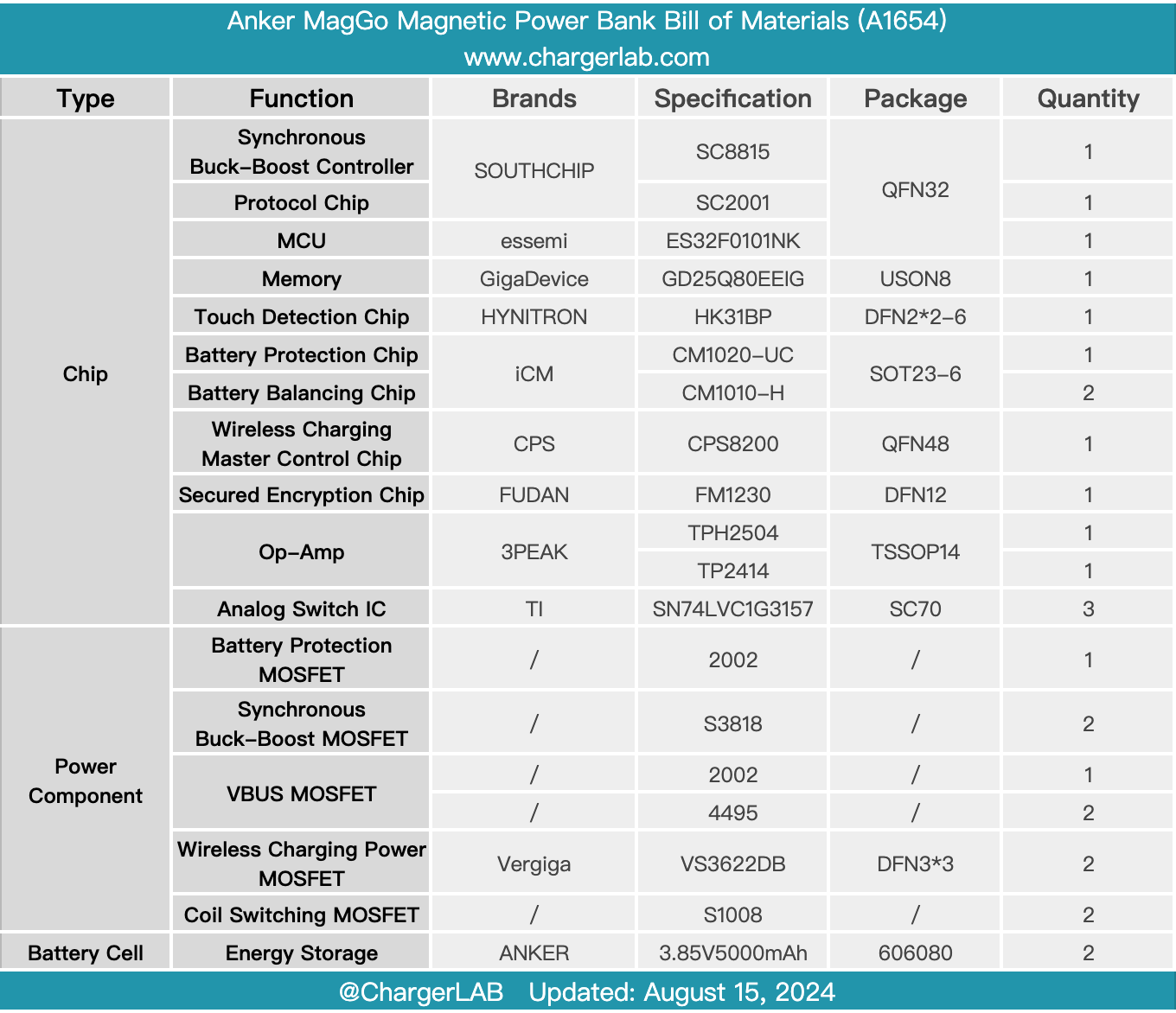
Here is the component list of the Anker MagGo Magnetic Power Bank for your convenience.
The Anker MagGo power bank has a flat design, a magnetic bracket on the back, and a compact size. There is a USB-C port on the side, which supports input of 20W and output of 27W and is equipped with an LCD display to show the remaining power and remaining usage time. It supports Qi2 protocol and the wireless charging power can reach 15W.
After taking it apart, we found it had two built-in lithium-ion polymer batteries. The wireless charging coil and the battery are isolated by an aluminum plate, and the battery edge is protected by foam. A graphite thermal pad is pasted inside the case to enhance heat dissipation. The battery protection chip is from iCM, with two battery balancing chips for overcharge, over-discharge, and over-current protection. It adopts thermistors for temperature detection. The overall workmanship of the power bank is fine and the materials used are solid.
Related Articles:
1. Teardown of CUKTECH 10000mAh 30W Power Bank (PB100)
2. Teardown of SHARGE 5000mAh Flow Mini Power Bank (SP012)
3. Teardown of IDMIX Q10 Pro 15W Magnetic Wireless Charging Power Bank with Stand

