Chargerlab Chargerlab
  • News
    • What's New
    • Interviews
    • Vlogs
    • Events
    • Industry
  • Reviews
    • Charging Compatibility
    • Fully Charging
    • Comparison
    • Chargers & Cables
    • Power Banks & Stations
    • Mobile Devices
    • Accessories
  • Teardowns
    • Chargers & Cables
    • Power Banks & Stations
    • Power Supplies
    • Prototypes
    • Batteries
    • Accessories
  • Videos
    • YouTube
    • TikTok
  • Guides
    • How to Buy
    • Explained
    • Deals
    • ICs
  • POWER-Z
    • KM003C/KM002C
    • KT002
    • Buy POWER-Z
    • Technical Support
  • Contact Us
Home › News › Industry › The New Innoscience 40V Bi-GaN Enhancement-mode FET
  • 1

The New Innoscience 40V Bi-GaN Enhancement-mode FET

Jeffrey
July 16, 2022

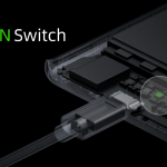
A short time ago, the Innoscience Bi-GaN series and the INN40W08 GaN switch transistor debuted.

The New Innoscience 40V Bi-GaN Enhancement-mode FET-Chargerlab

The Innoscience INN40W08 is a 40V enhancement-mode FET in the Bi-GaN series in a WLCSP 2x2 package with a very compact size. The chip supports bi-directional blocking capability with resistance as low as 7.8mΩ and can be used to protect circuits in an overvoltage when charging. Or it can apply to the high side electrical load switch circuits and switch circuits for multi-power suppliers system.

ChargerLAB learned that OPPO has already adopted the GaN switch transistor in mass production, becoming the first phone manufacturer with built-in GaN charging protection worldwide, which has extraordinary significance in the industry.

Highlights

Due to the limit of volume and resistance, the silicon MOSFET not only occupies a large amount of space on the phone's main board but also generates considerable temperature rise and efficiency loss when facing high power fast charging, affecting the stability and high power duration of fast charging.

As a third-generation semiconductor material, GaN has advantages of high frequency, high efficiency, low resistance, and so on, which plays a crucial role in charging. Previously, charging protection was done by integrating GaN components into chargers, while Bi-GaN is to build GaN FETs into phones.

The New Innoscience 40V Bi-GaN Enhancement-mode FET-Chargerlab

Thanks to the small thermal resistance per unit area of GaN and the diode, one Bi-GaN can be used to replace the previous NMOS to realize a bi-directional switch of the currents of charging and discharging, reducing on-state resistance by 50% and temperature rise by 40% in the same occupied board area.

As the charging power of phones continues to rise, the Innoscience Bi-GaN series not only save valuable space inside the phone but also reduces the temperature rise of the phone during charging, maintains a more comfortable temperature during fast charging, extends the duration of fast charging, and provides users with a better charging experience.

Summary of ChargerLAB

The Innoscience INN40W08 is a 40V enhancement-mode FET in the Bi-GaN series in a WLCSP 2x2 package with a very compact size. The chip supports bi-directional blocking capability with resistance as low as 7.8mΩ and can be used to protect circuits in an overvoltage when charging. Or it can apply to the high side electrical load switch circuits and switch circuits for multi-power suppliers system.

As the charging power of phones continues to rise, the Innoscience Bi-GaN series not only save valuable space inside the phone but also reduces the temperature rise of the phone during charging, maintains a more comfortable temperature during fast charging, extends the duration of fast charging, and provides users with a better charging experience.

Related Articles:
1. UGREEN Launches The New 45W Dual-port GaN Charger (Simultaneous Fast Charging for Dual iPhones)
2. Review of Asus Adol 100W GaN Charger
3. Review of UGREEN Nexode 3-in-1 65W GaN Charger

GaN OPPO
1
Teardown of Zikko Thunderbolt 4 Cable (0.8m)
Previous
Teardown of InfinityLab ILINC 100W 2A2C GaN Charger
Next

Hot posts

100W+ PPS | Charging Compatibility Test of REDMAGIC 11S Pro+
Teardown of the NVIDIA DGX Spark Original 240W USB-C Power Adapter
1080W Peak Power | An In-Depth Analysis of Silicon Carbide Chargers from 26 Brands
Chipown’s PN8602 Boosts Efficiency and Lowers GaN Operating Temperatures in PD Chargers

Related posts

Over 360 Qi2-certified Products! 90 New Qi2 Products Added in June

Over 360 Qi2-certified Products! 90 New Qi2 Products Added in June

July 31, 2024
0
Navitas Selected for NVIDIA’s Next-Gen 800V HVDC Data Center Architecture

Navitas Selected for NVIDIA’s Next-Gen 800V HVDC Data Center Architecture

June 7, 2025
0
CALB Takes Center Stage at Shenzhen’s Premier UAV Industry Event

CALB Takes Center Stage at Shenzhen’s Premier UAV Industry Event

May 25, 2026
0
Deep Dive of Charging Compatibility of the AMC 240W GaN Charger

Deep Dive of Charging Compatibility of the AMC 240W GaN Charger

May 21, 2026
0
1

ABOUT US

As a sibling site of chongdiantou.com, ChargerLAB covers everything about charging, including chargers, wireless chargers, power banks, cables, car chargers, portable power stations and other peripherals. You can contact us by sending the email to info@chargerlab.com.

FOLLOW US

Facebook Instagram TikTok Twitter YouTube

E-COOL MEDIA

POWER-Z PowerPi Chongdiantou 52Audio
Copyright © 2016-2026 Chargerlab. Designed by nicetheme.
  • News
    • What's New
    • Interviews
    • Vlogs
    • Events
    • Industry
  • Reviews
    • Charging Compatibility
    • Fully Charging
    • Comparison
    • Chargers & Cables
    • Power Banks & Stations
    • Mobile Devices
    • Accessories
  • Teardowns
    • Chargers & Cables
    • Power Banks & Stations
    • Power Supplies
    • Prototypes
    • Batteries
    • Accessories
  • Videos
    • YouTube
    • TikTok
  • Guides
    • How to Buy
    • Explained
    • Deals
    • ICs
  • POWER-Z
    • KM003C/KM002C
    • KT002
    • Buy POWER-Z
    • Technical Support
  • Contact Us
  • Apple
  • GaN
  • ANKER
  • Power Bank
  • 100W
  • 65W
  • ChargerLAB
  • Xiaomi
  • Baseus
  • UGREEN

Jeffrey

Author