Introduction
Just a few months ago, we conducted a charging compatibility test of the Xiaomi 13 Pro, which included a 120W charger. If you are a Xiaomi fan, then you probably know that they tend to pair their flagship phone with a non-flagship wired charging speed. For instance, the latest Xiaomi 13 Ultra has a maximum power of only 90W. However, Xiaomi has valid reasons for doing this - to free up more valuable space in the phone and allocate it towards the camera module, which is a standout feature of the Xiaomi 13 Ultra flagship.
However, in terms of compatibility, this 90W charger is actually not too shabby. Not only does it support Xiaomi's 90W proprietary fast charging protocol, but when paired with the dedicated USB-A to USB-C cable, it can also support 65W PD fast charging output, which is super rare for a USB-A charger. Next, ChargerLAB will take apart this Xiaomi 90W GaN charger to reveal its internal components and build quality.
Product Appearance
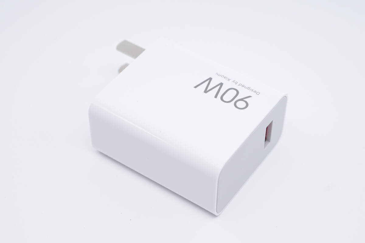
It adopts a white glossy PC design, which is a classic design of Xiaomi charger.
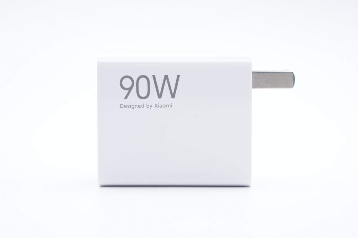
A big "90W" is printed on the side.
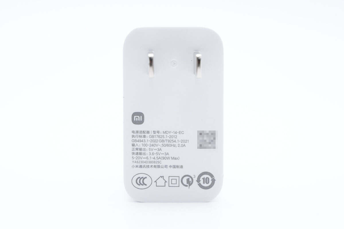
And the specs info is under the fixing two-prong plug, as always.
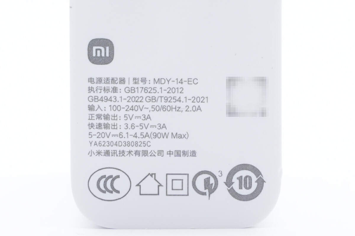
Model is MDY-14-EC. It can support input of 100-240V~50/60Hz 2A, and the maximum output is 90W. It also has passed Qualcomm QC3.0 certification.
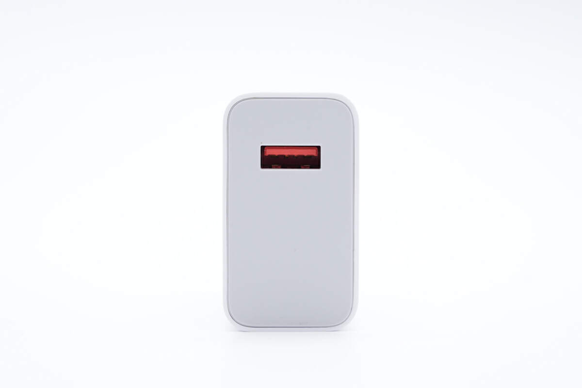
It still adopts the same old special design USB-A port with a red plastic sheet.

Take a closer look, we can see two widened pins, which are the key to achieveing PD output on the USB-A port.
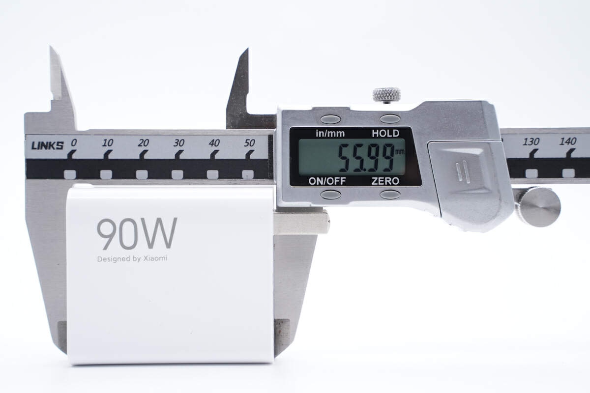
The length of the charger is about 56mm (2.20 inches).
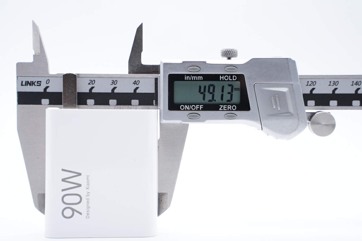
The width is about 49.1mm (1.93 inches).

And the height is about 27.9mm (1.10 inches), so the power density is about 1.17W/cm³.
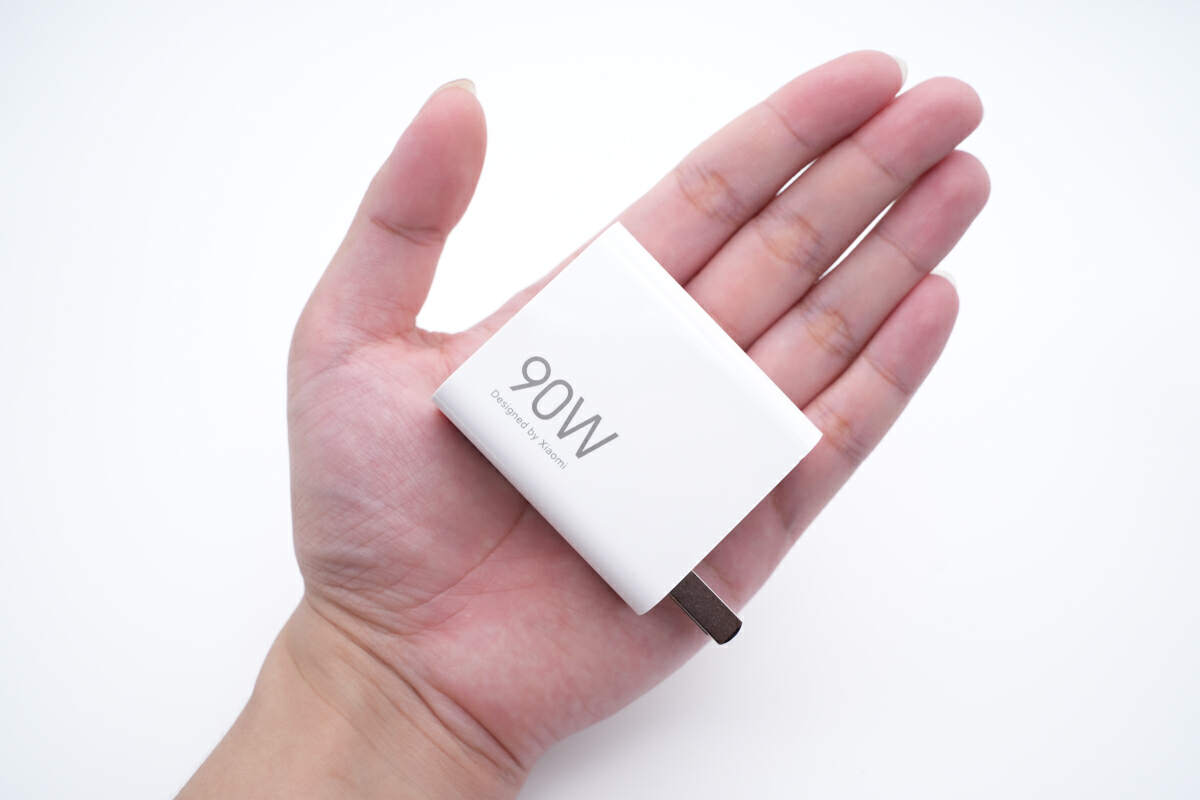
This is what it looks like on my hand, pretty tiny.
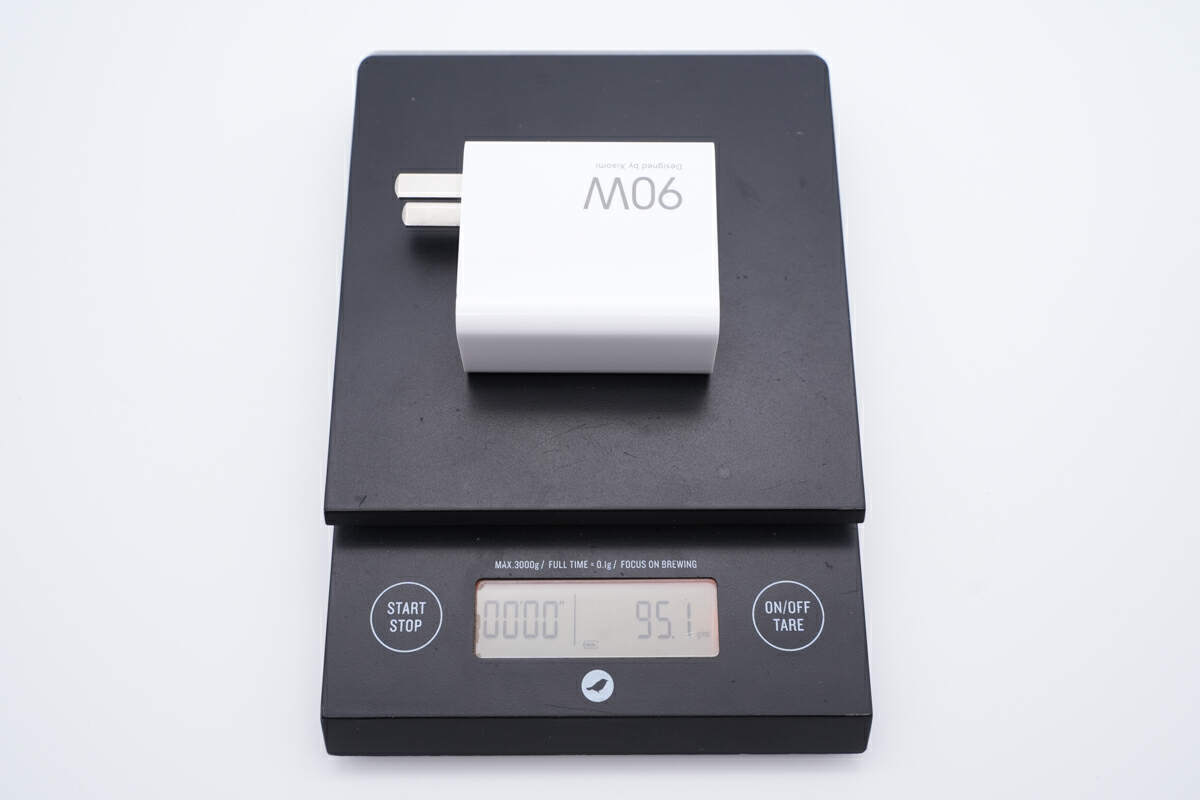
And the weight is about 95g (3.35 oz).
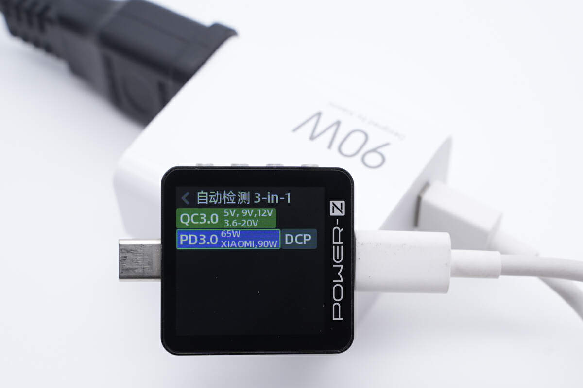
The ChargerLAB POWER-Z KM003C shows the charger not only supports QC3.0, PD3.0, DCP protocols, but also the Xiaomi's 90W protocol.
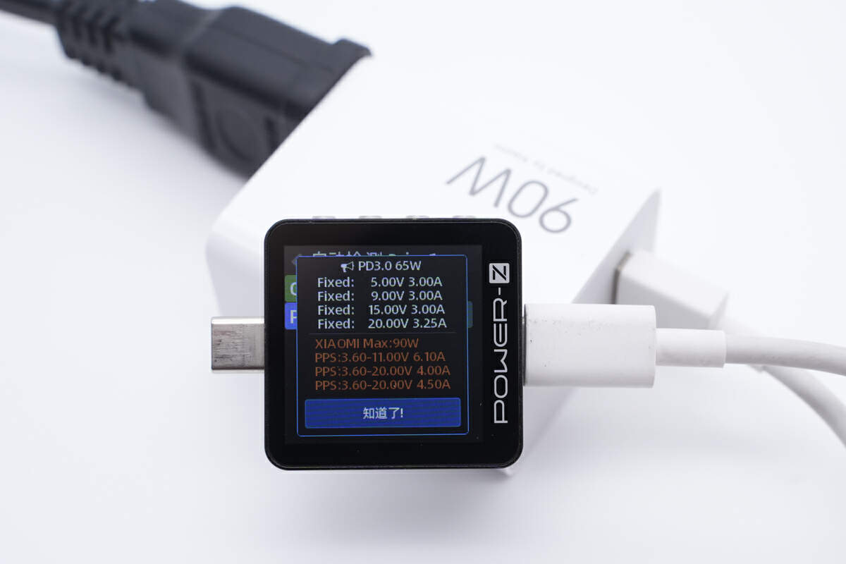
And it also has four fixed PDOs of 5V/9V/15V 3A, 20V 3.25A, and three sets of proprietary PPS.
Teardown
Now that we have completed our unboxing and testing of this Xiaomi charger, it's time to take apart the device and examine its internal components and structure.
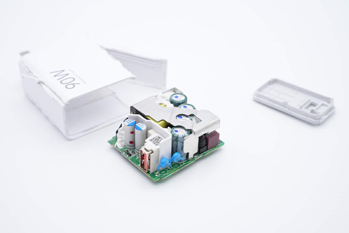
Use the cutting machine to cut off the outer case, and take out the PCBA module.
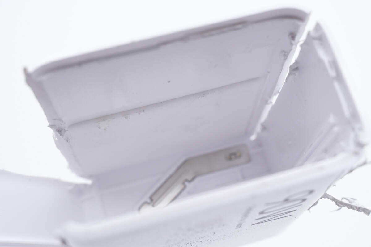
There are some foams inside the case for buffering.
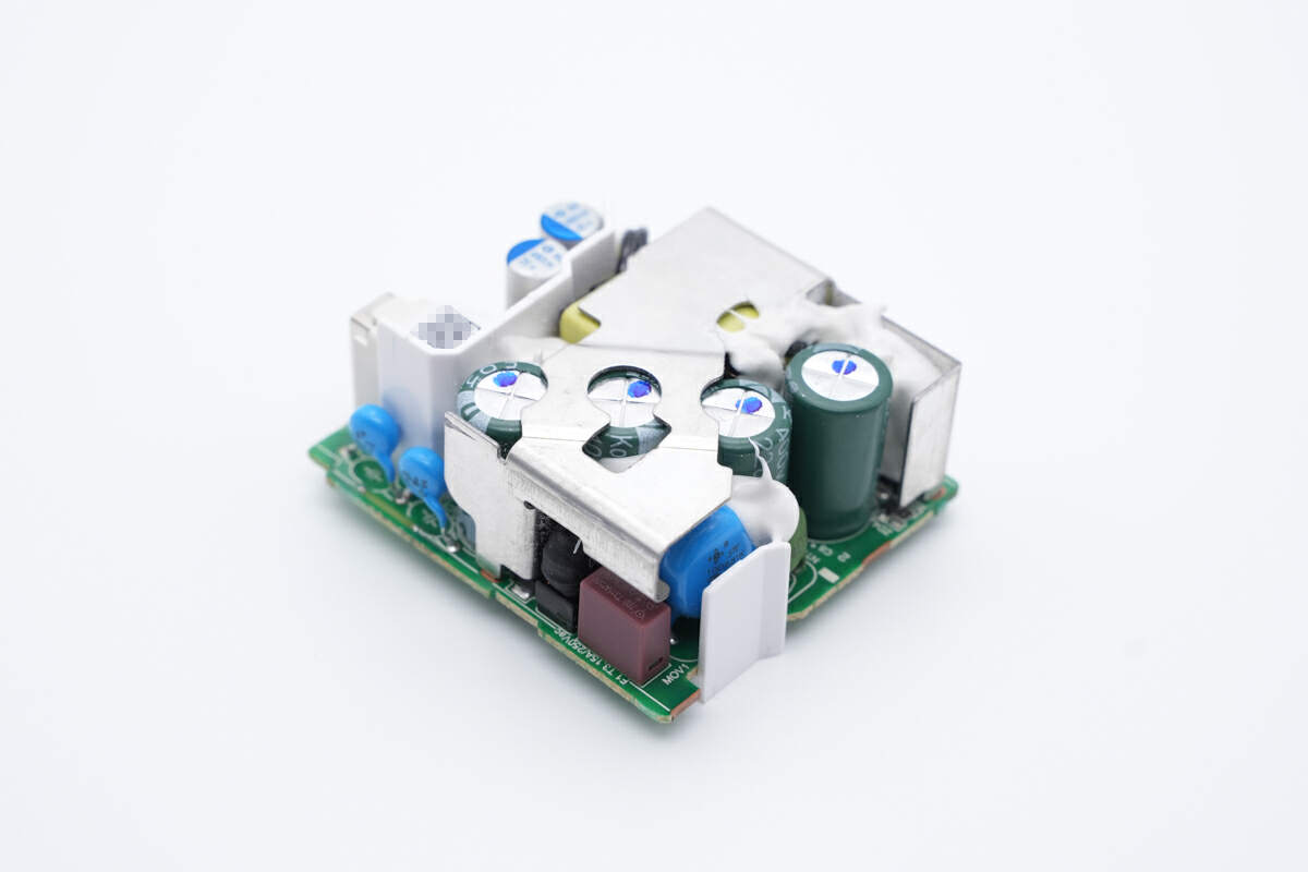
And the PCBA module is wrapped by a layer of irregular heat sink.
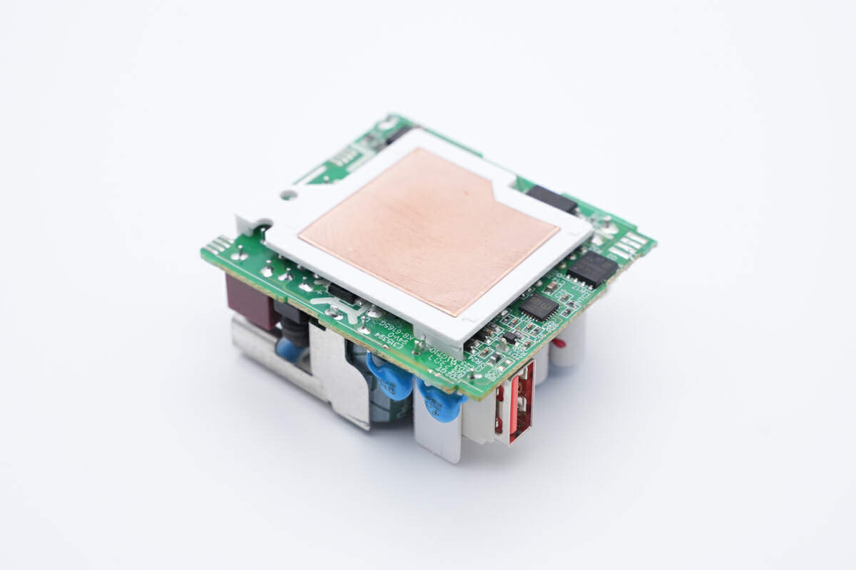
A combination of plastic board and copper foil are located on the back for heat dissipation.
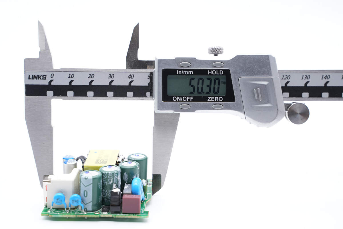
The length of the PCBA is 50.3mm (1.98 inches).
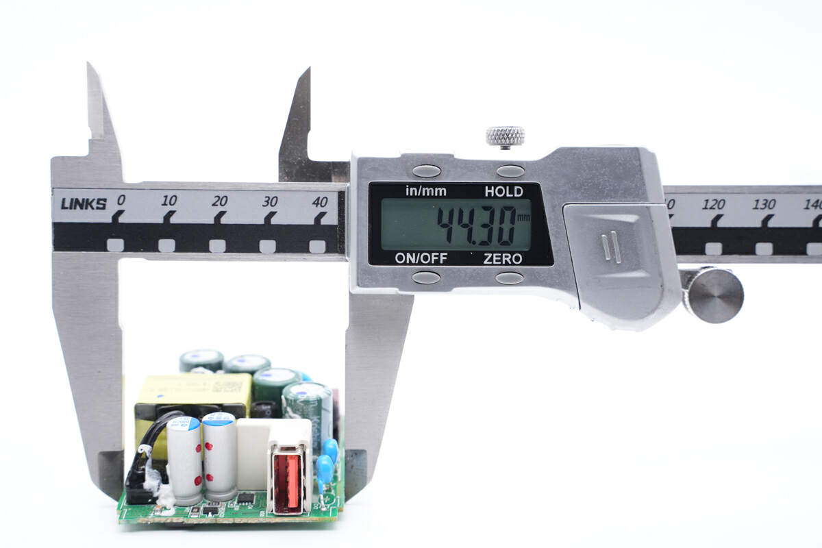
The width is 44.3mm (1.74 inches).
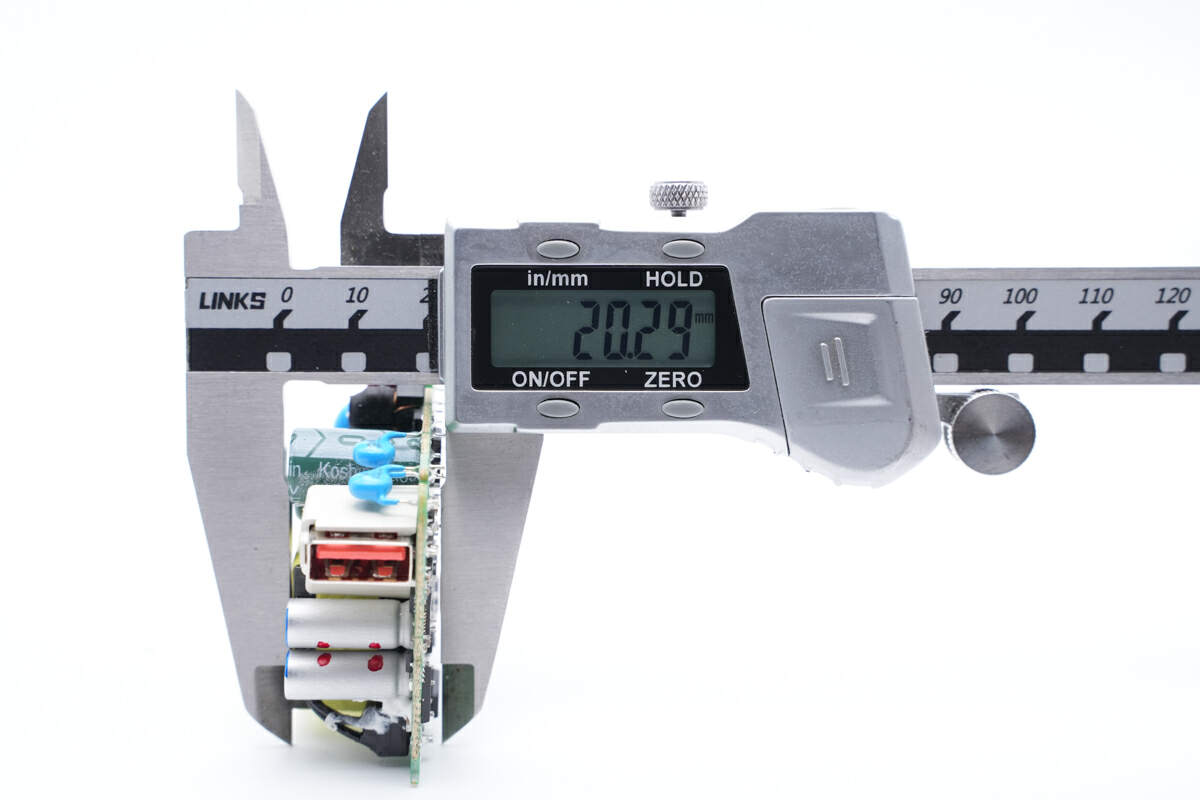
And the height is about 20.3mm (0.80 inches).
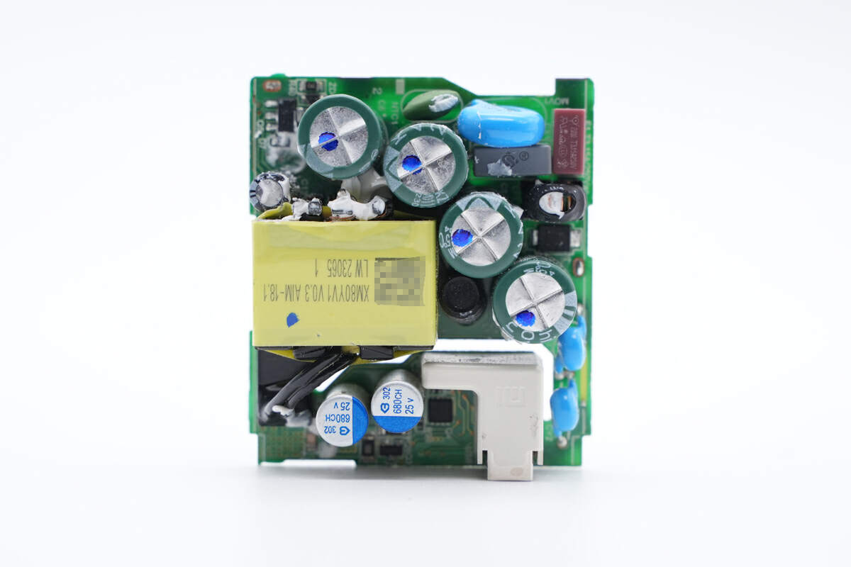
The fuse, NTC thermistor, common mode choke, high voltage filter capacitor and transformer are on the front of PCBA module.
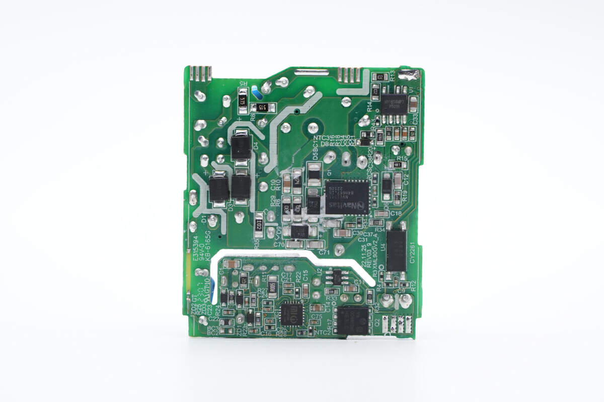
And rectifier diode, master control chip, feedback optocoupler, synchronous rectifier controller, protocol chip and synchronous rectifier MOSFET are on the back.
ChargerLAB found that this Xiaomi 90W GaN charger adopts QR flyback topology, and the output voltage is controlled by the protocol chip. Both the switch-mode power supply controller and the synchronous rectifier controller are from Hyasic Semi, the GaN IC is from Navitas, and the protocol chip is from Injoinic. Next, let's introduce all the major components.
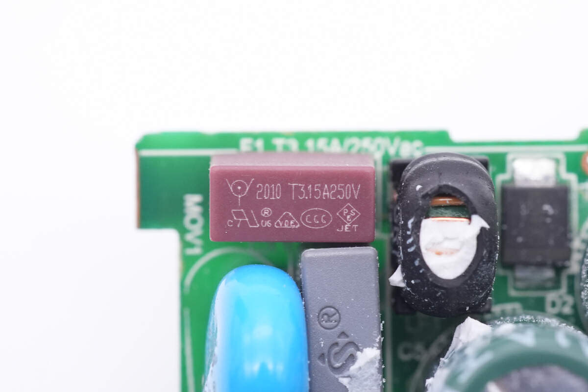
The input time-delay fuse is from WalterFuse. 3.15A 250VAC.
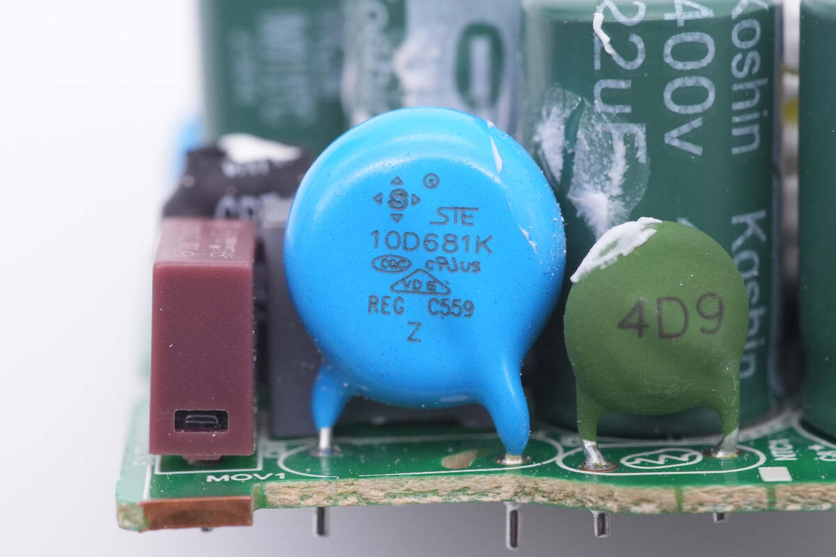
The varistor is from STE, model 10D681K, which is used to absorb the surge overvoltage.
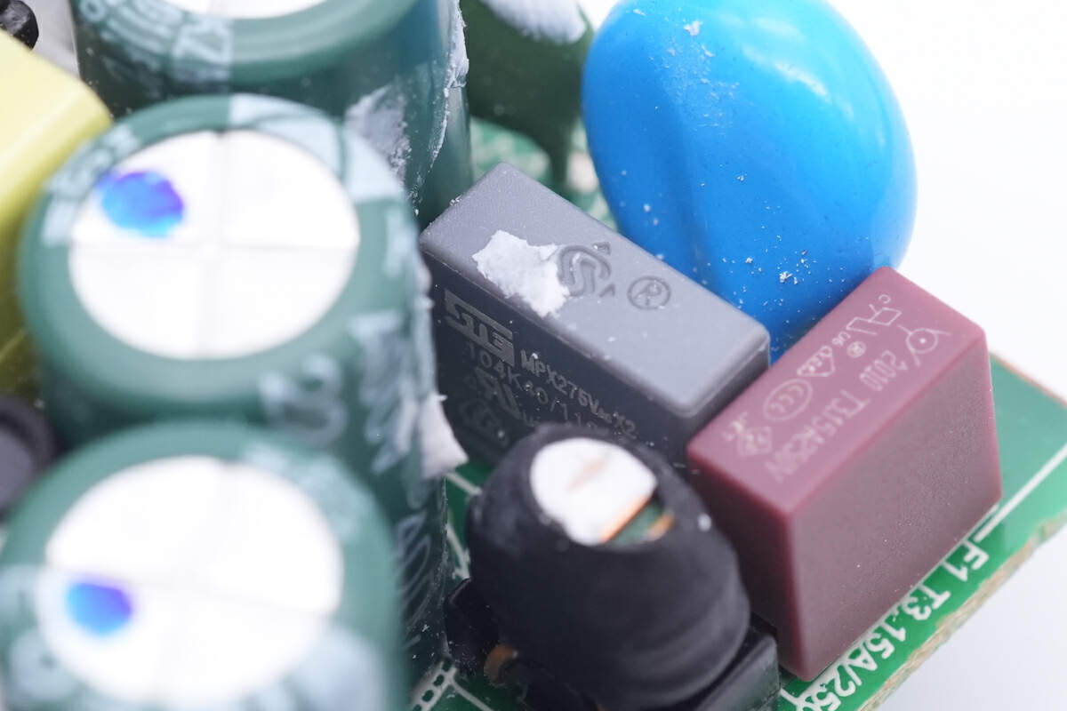
And the safety X2 capacitor behind it is from STE. 0.1μF.
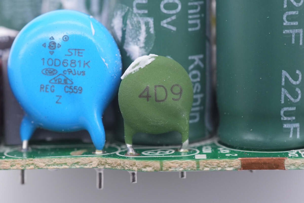
The NTC thermistor marked with 4D9 is used to suppress the surge current.
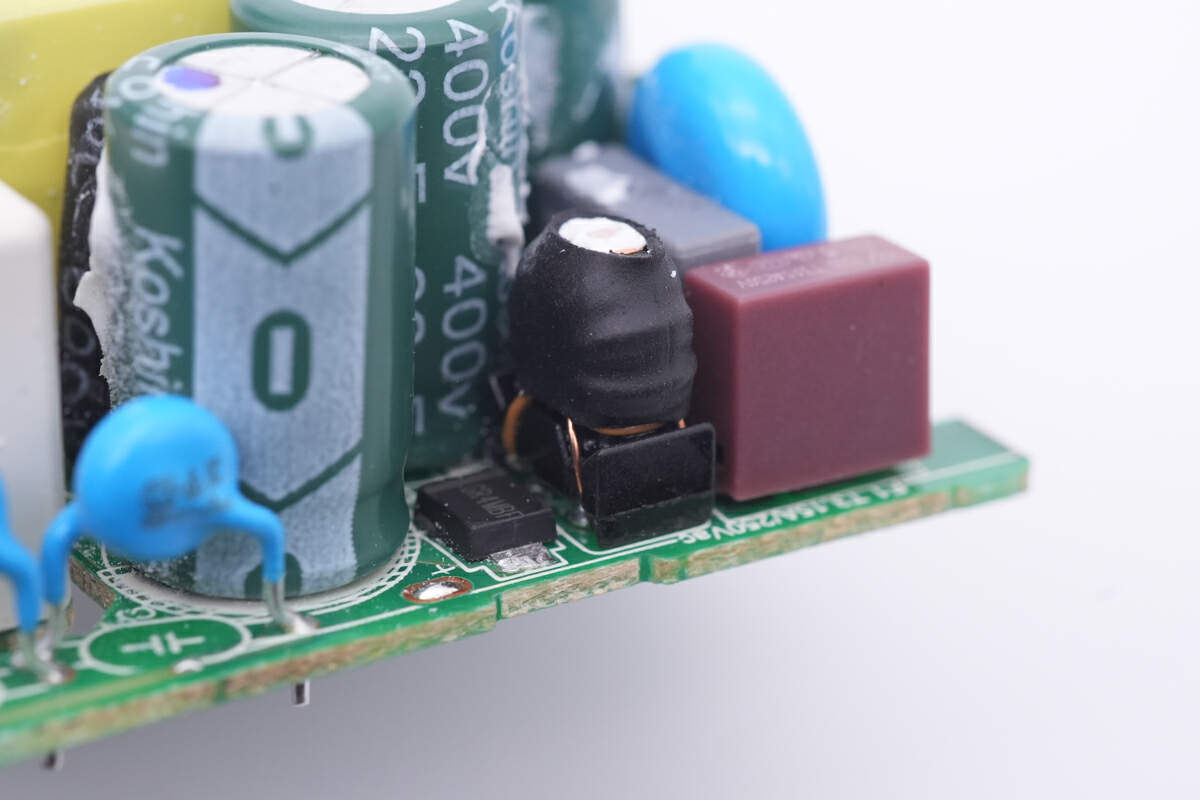
The common mode choke is insulated with heat-shrinkable tubing.
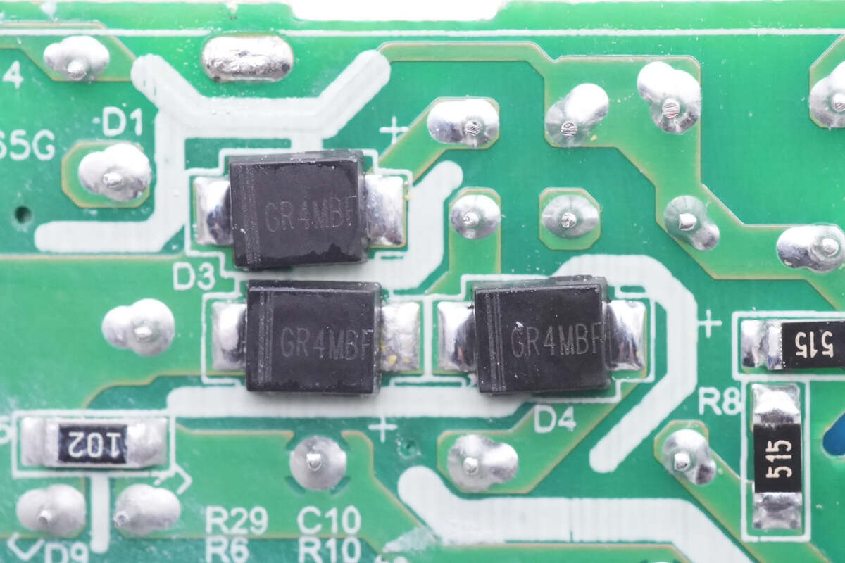
Surprisingly, it doesn't use a separate bridge rectifier, but instead uses four diodes to form a bridge rectifier, with three of them soldered on the back of the PCB. This design optimizes the use of space, making it easy to shrink the charger's size.
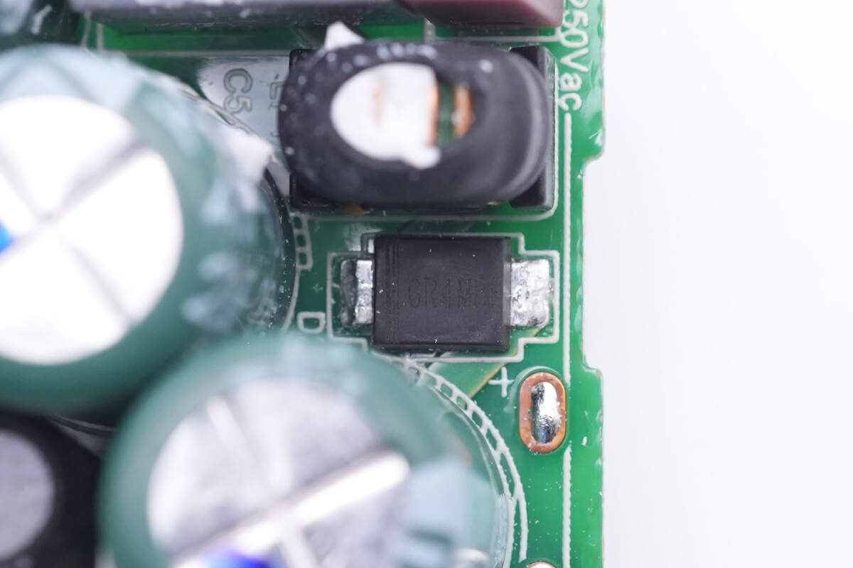
The last one is located next to the common mode choke we just mentioned, model GR4MBF, which is a 4A 1000V fast recovery diode.
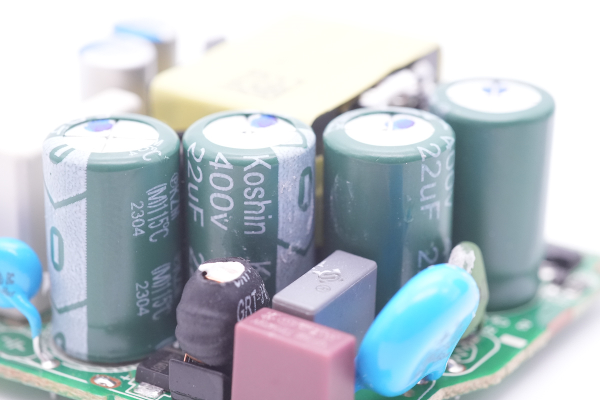
These four high-voltage filter capacitors are from Koshin. 400V 22μF.
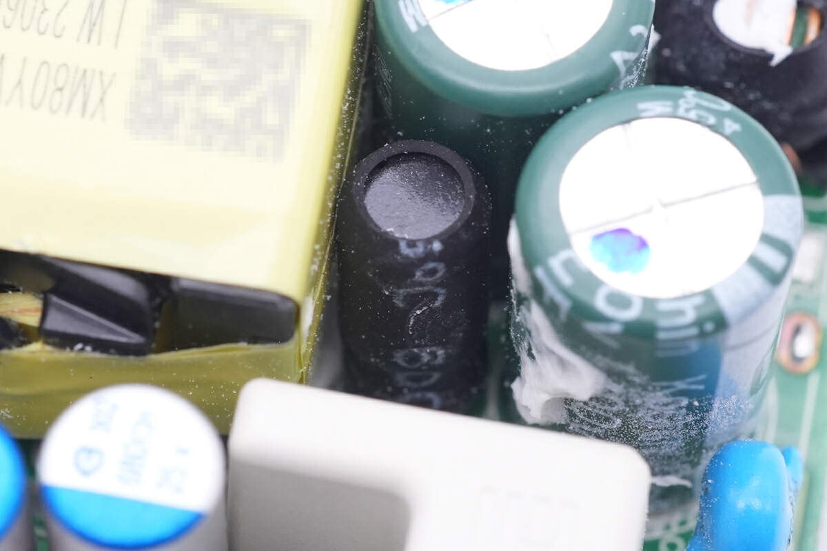
And the differential mode choke next to them adopts I-shaped magnetic core and is insulated with heat-shrinkable tubing.
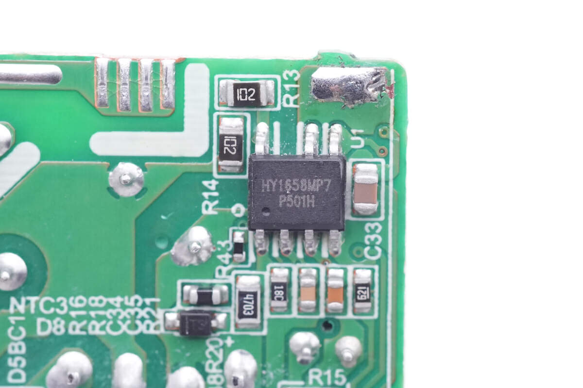
The master control chip is from Hyasic Semi, model HY1658M, which is an intelligent multi-mode Flyback controller with high voltage start up, and adopts SOP7L package. It can support multiple working modes, and can automatically switch between QR and CCM modes to balance the switching loss and the conduction loss. The chip also has switching frequency dithering to improve EMI performance, the adaptive MOSFET gate driver can balance switching loss and EMI.
Furthermore, the HY1658M integrates rich protections and features such as output overvoltage protection, transformer saturation protection, undervoltage/overvoltage protection, overload protection, over temperature protection and current sensing open protection. It is suitable for USB PD charger, TV/monitor standby power and notebook power.
An NTC thermistor is in the lower left corner of the chip, which is used for overheat protection.
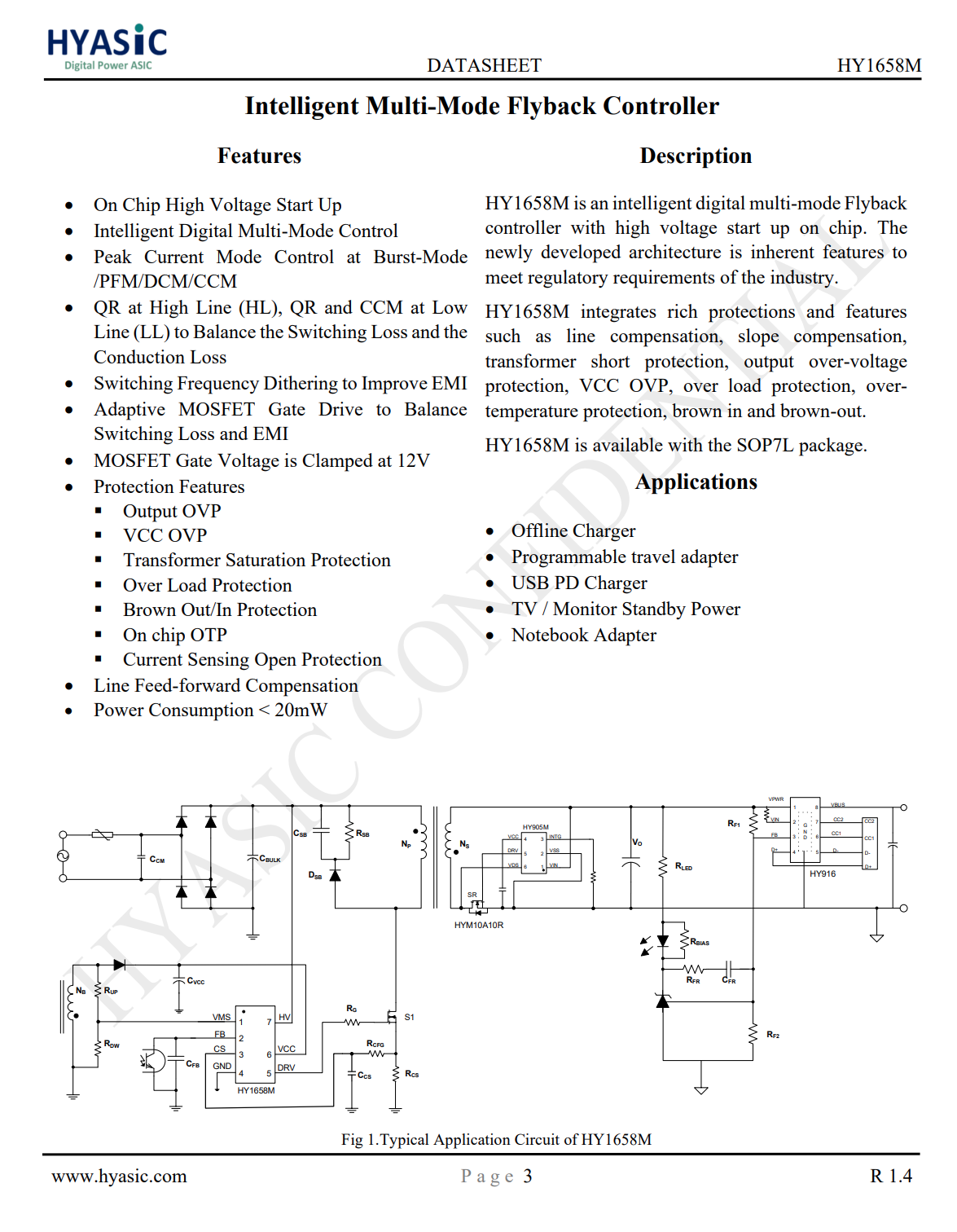
Here is all the information about Hyasic Semi HY1658M.
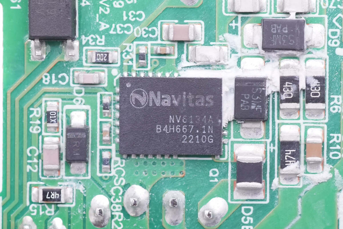
The highly integrated GaN IC is from Navitas and adopts QFN6 x 8 package. It integrates GaN FET, driver, and lossless current sampling circuit, which can eliminate the loss of the sampling resistor. Model is NV6134A.
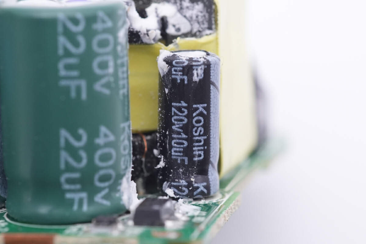
The electrolytic capacitor that powers the master control chip is also from Koshin. 120V 10μF.
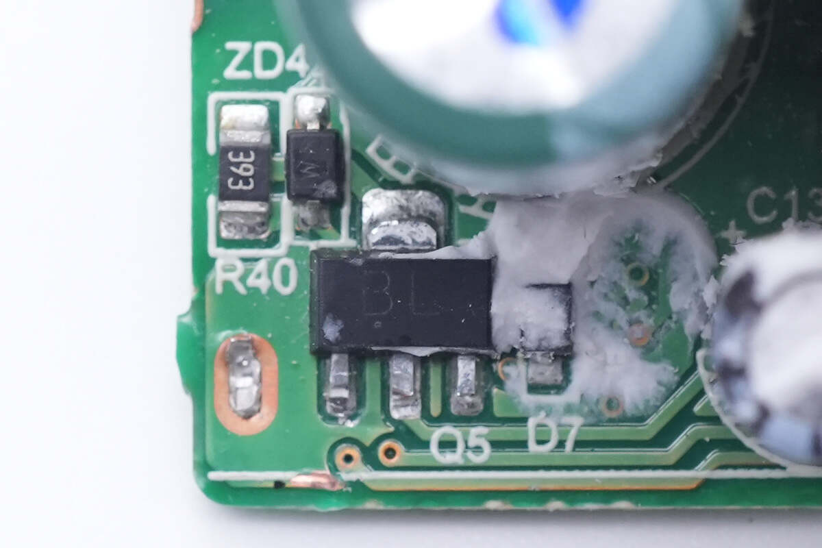
A triode marked with BL is used for power supply regulation.
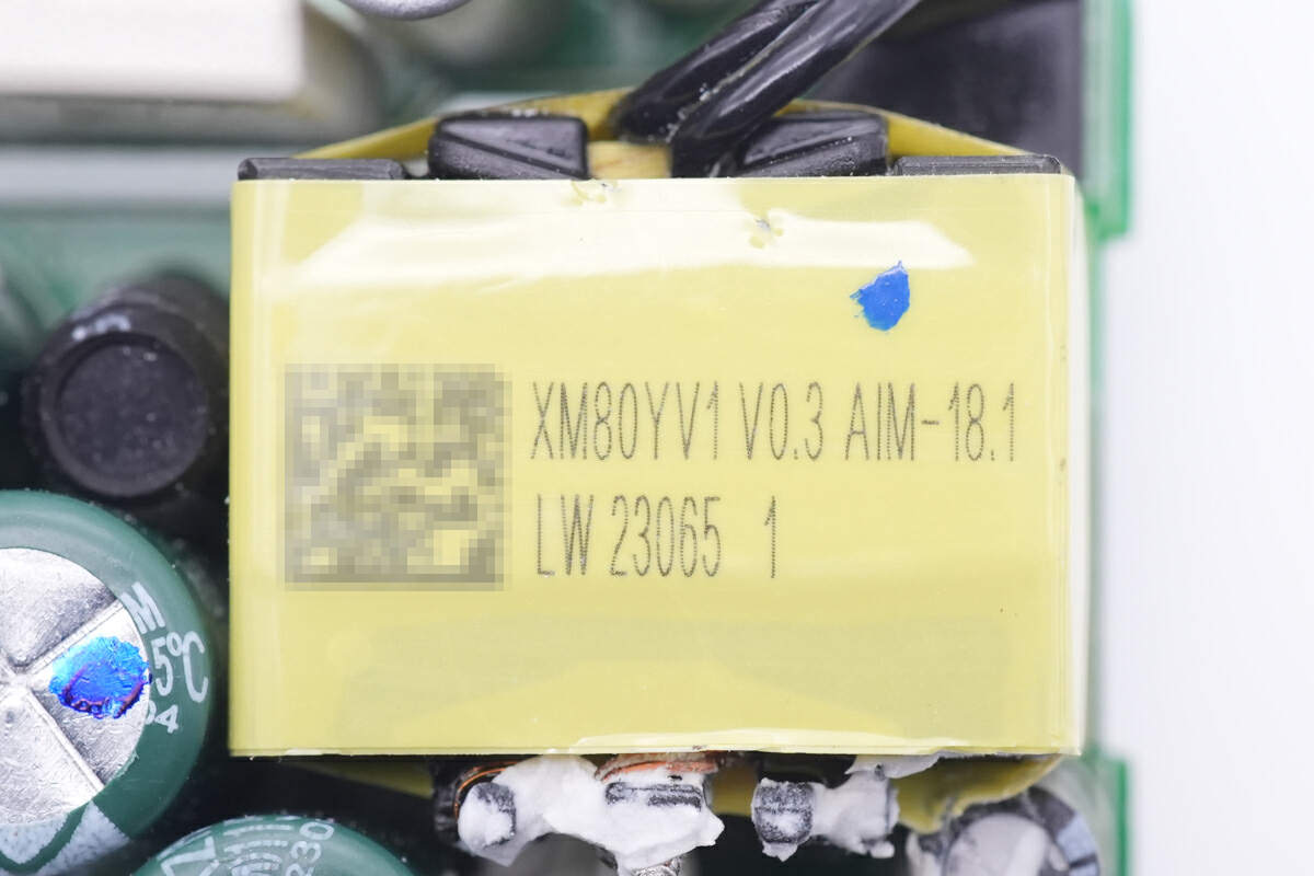
The transformer is wrapped with yellow tape.
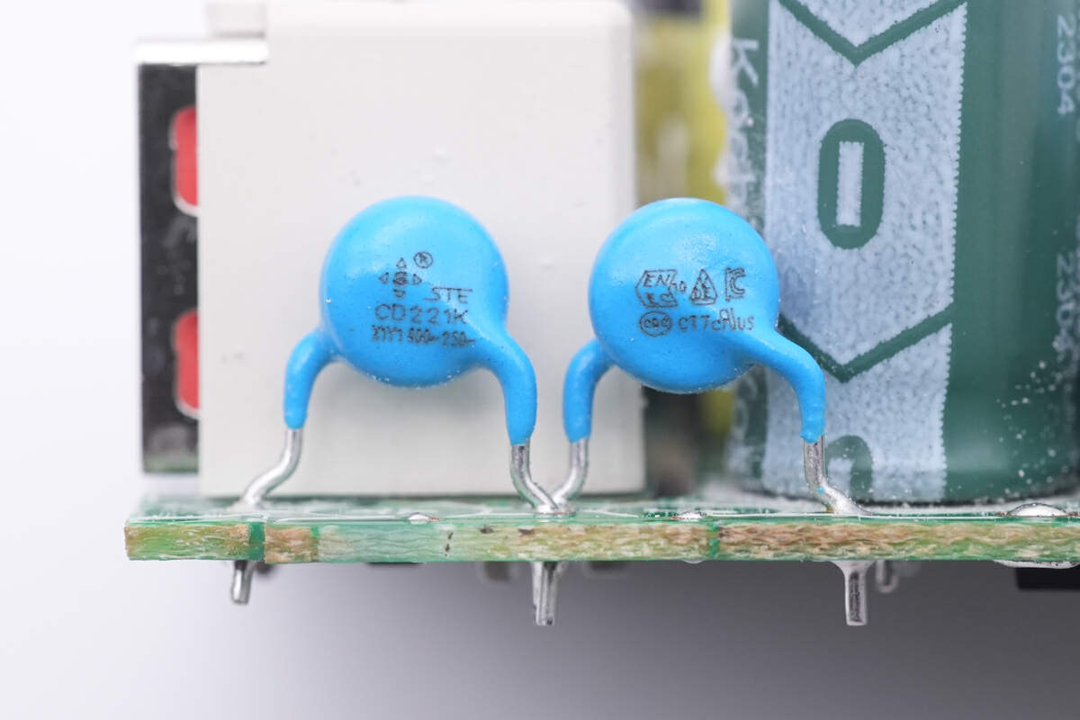
And These two blue Y capacitors are also from STE.
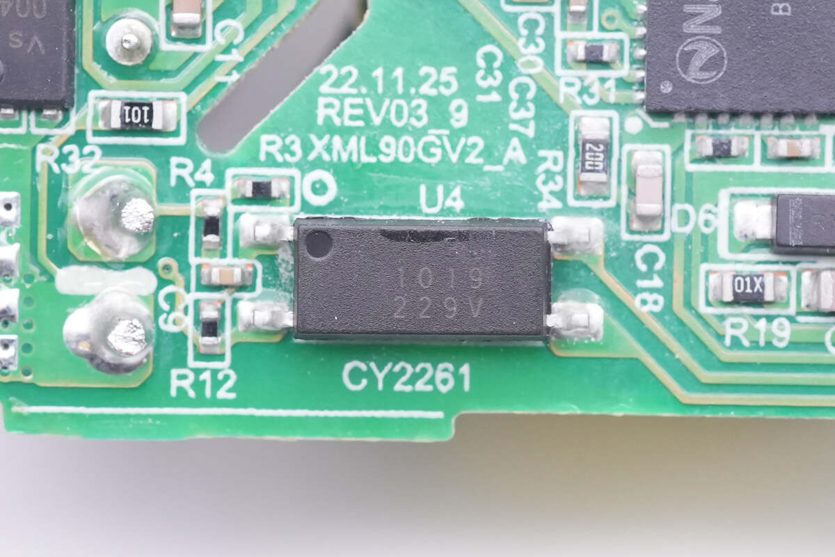
The EL1019 optocoupler is from EVERLIGHT, which is used to regulate the output voltage.
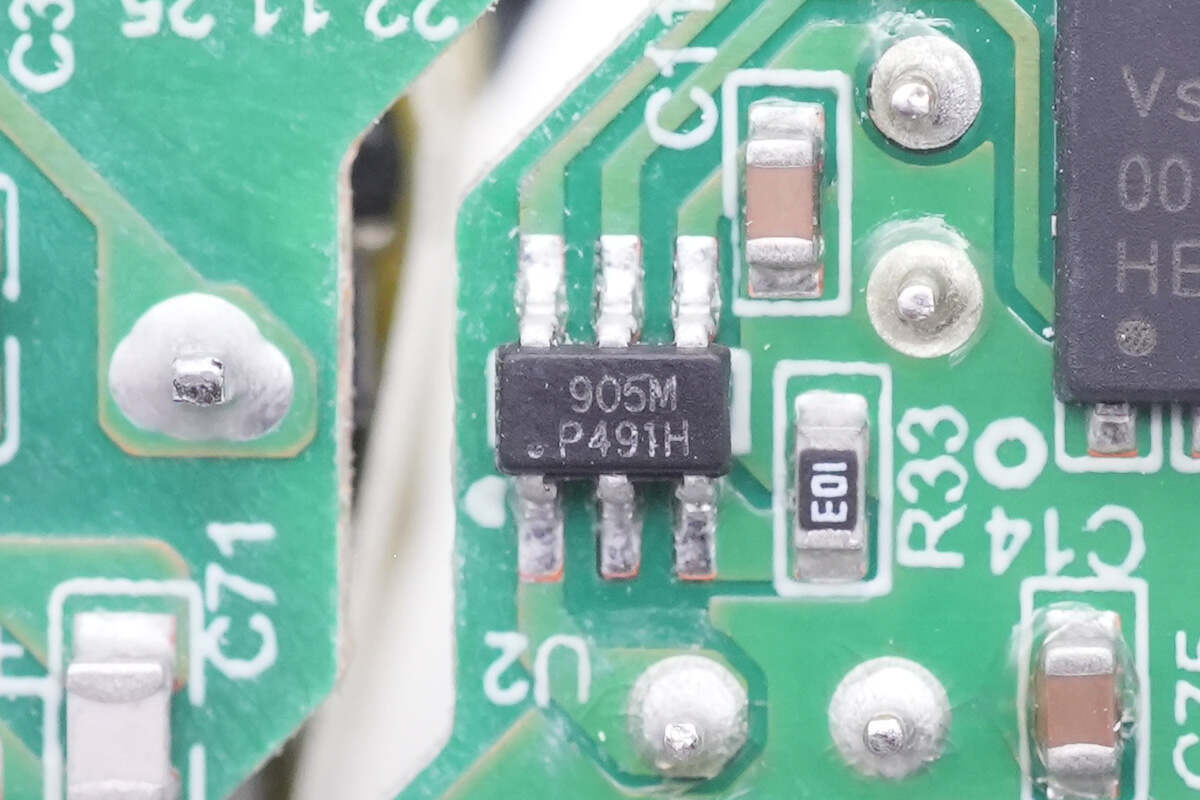
The synchronous rectifier controller is also from Hyasic Semi, model HY905M, which is a digital adaptive multi-mode controller and adopts SOT23-6 package. It can support low-side synchronous rectification without auxiliary winding. And it also supports multiple working modes such as DCM, CCM, PFM and QR, the output voltage range is pretty wide at 3.2-25V. It features adaptive pre-turn off drive for faster turn off transition.
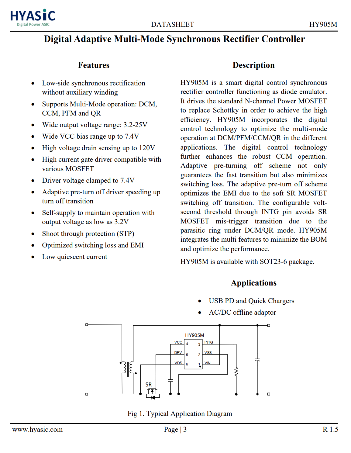
Here is all the information about Hyasic Semi HY905M.
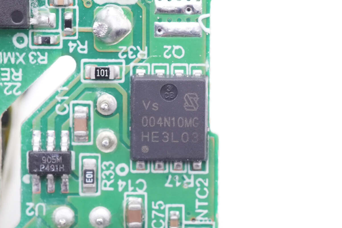
The synchronous rectifier MOSFET is from Vergiga Semi and adopts PDFN5060X package. Model is VSP004N10MS-G. 100V 3.8mΩ.
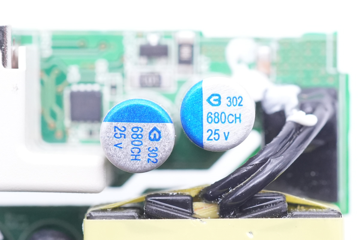
These two solid capacitors for output filtering are from Beryl CH series. 680μF 25V.
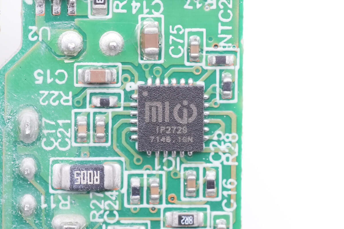
The protocol chip is from Injoinic, model IP2729, which is customized by Xiaomi. It integrates USB PD, QC3.0 and Xiaomi 120W fast charging protocols, which is very powerful.
And a thermistor is located in the lower left corner of the protocol chip, which is used to detect the internal temperature rise of the charger and protect it from overheating.
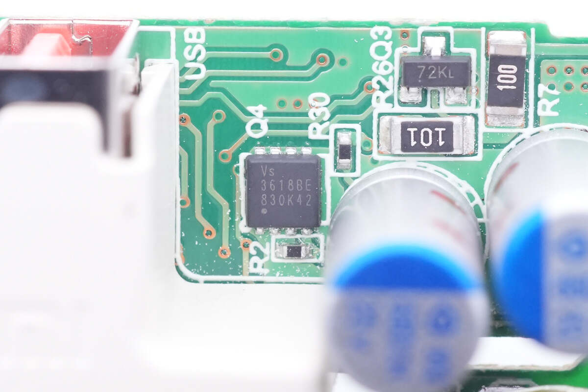
The VBUS MOSFET of the USB-A port is also from Vergiga Semi and adopts PDFN3333 package. Model is VS3618BE. 30V 5.2mΩ.
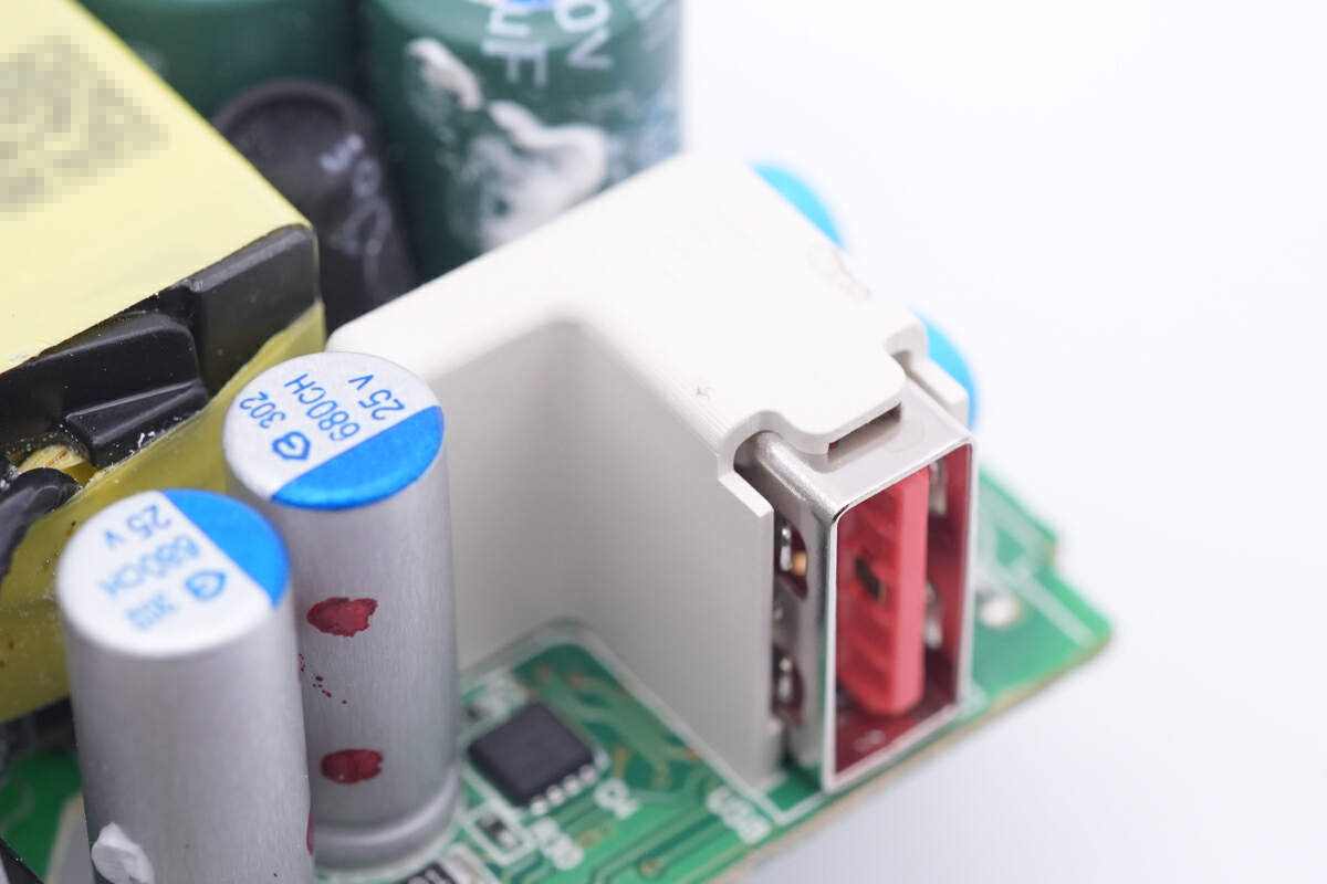
The USB-A socket is L-shaped and reinforced with a plastic shell.
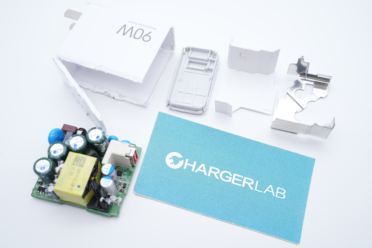
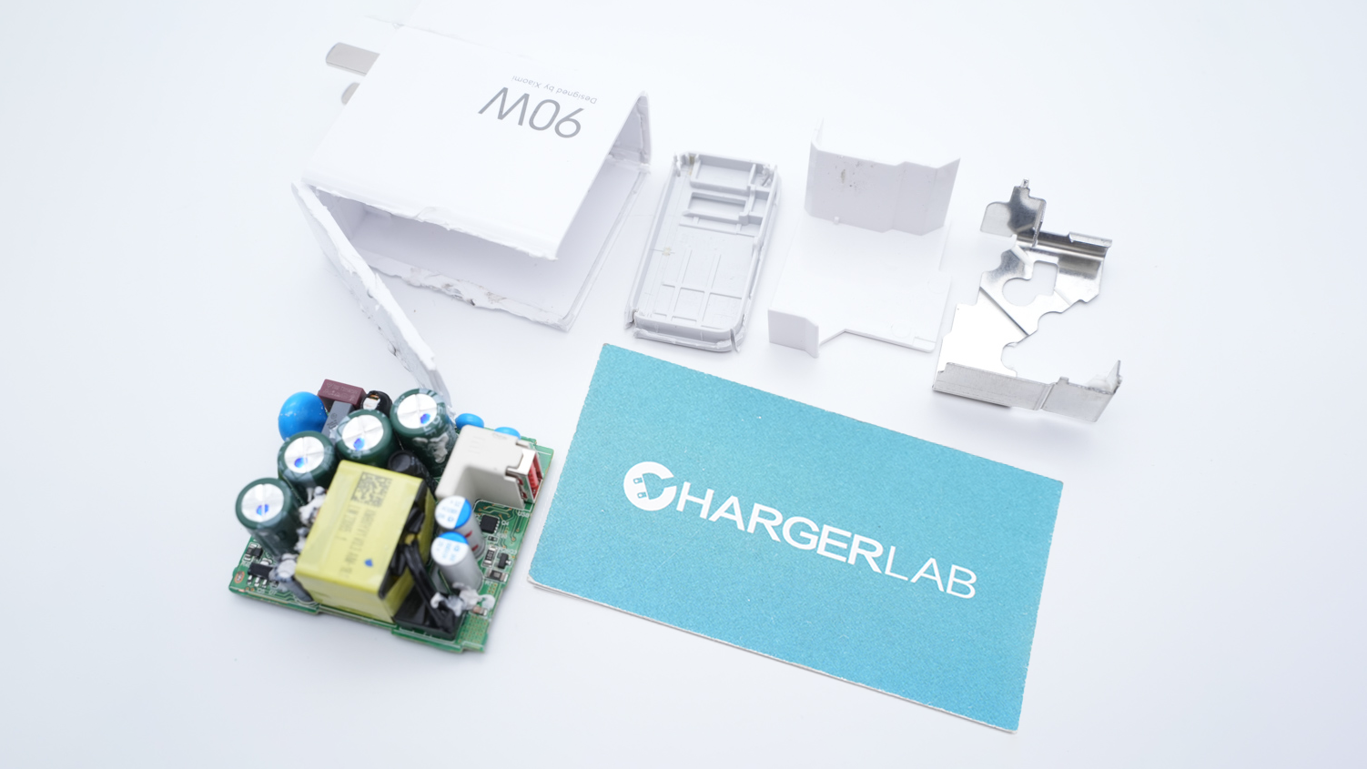
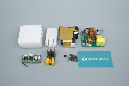
One last look at all the components of this Xiaomi 90W GaN Charger.
Summary of ChargerLAB
In conclusion, the Xiaomi 90W GaN charger is a well-designed and compact charger with excellent compatibility and performance. Our teardown of the device revealed that it adopts high-quality components, including a Hyasic Semi master control chip, Navitas GaN IC, Injoinic protocol chip, and Beryl solid capacitors. Additionally, the charger supports multiple fast charging protocols, including Xiaomi's proprietary 90W fast charging protocol, QC3.0, and PD3.0. The innovative design of this charger optimizes space utilization by integrating the four diodes to form a bridge rectifier, making it smaller in size. Overall, this charger is a great option for anyone looking for a reliable and high-performance charger for their Xiaomi devices.
Related Articles:
1. Charging Compatibility Test of Xiaomi 13 Ultra
2. Teardown of Xiaomi 90W GaN Charger (Video)
3. A Shot Above | Xiaomi 13 Ultra Launch Event

