Introduction
Several weeks ago, ChargerLAB posted a charging compatibility test video of the vivo X90 Pro, and it comes with a 120W flash charge charger. This charger not only supports vivo's proprietary fast charging protocol and 65W PD, but also has a customized GaN power chip by Innoscience, making it both compact and powerful. And today, we're going to take it apart and reveal its internal components and build quality.
Product Appearance
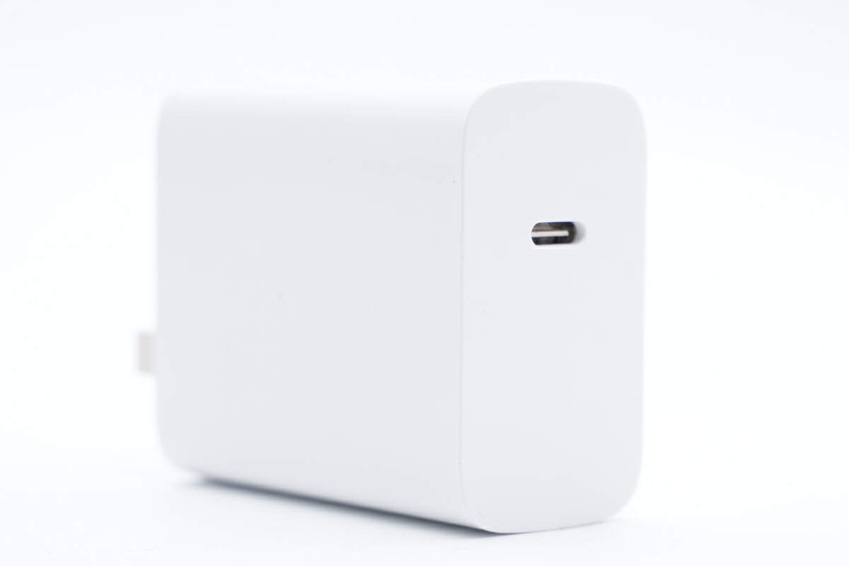
The output port of this charger is a single USB-C.
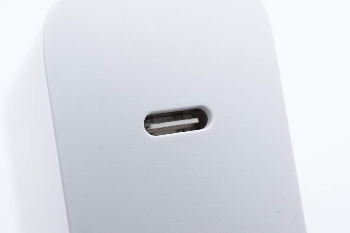
And the plastic sheet inside the USB-C socket is white.
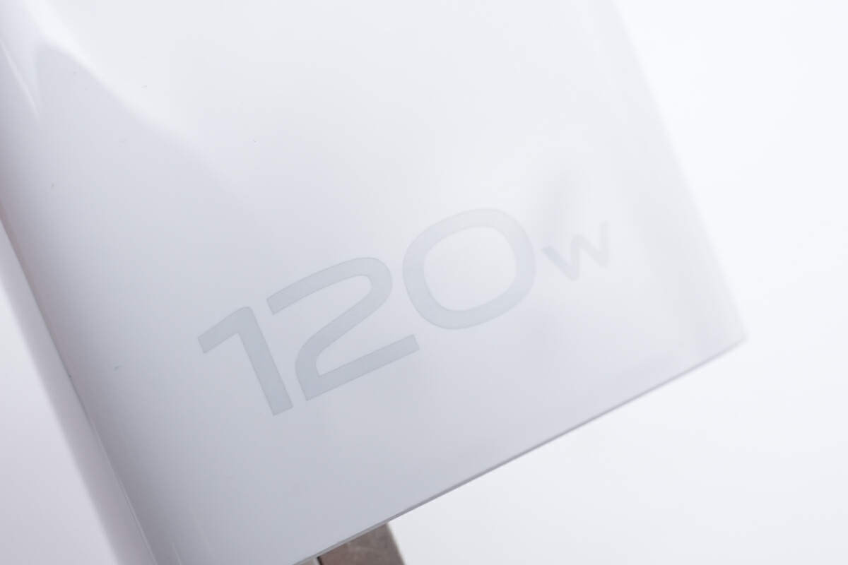
The "120W" is clearly printed on glossy white plastic.
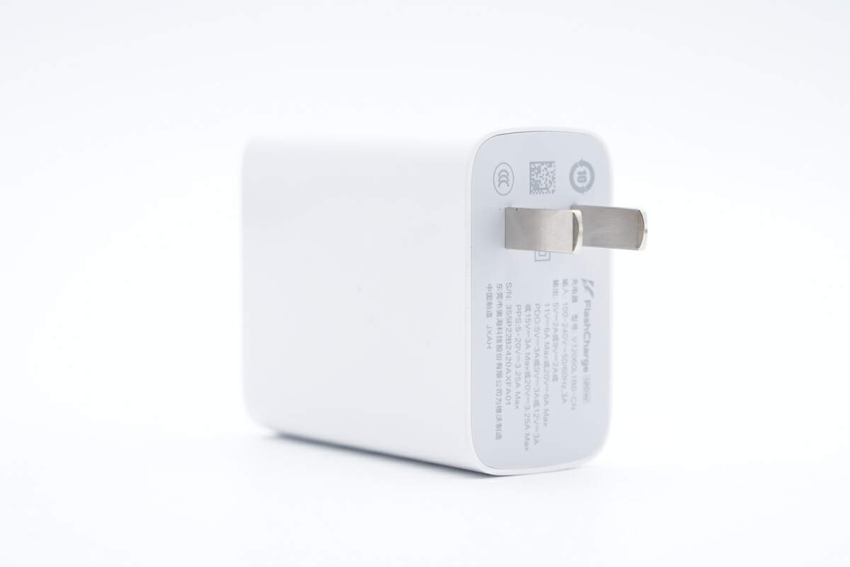
All spec info is printed below the fixed input prongs.
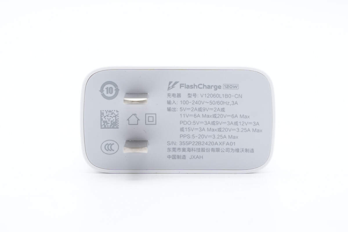
Model is V12060L1B0. It supports input of 100~240V~50/60Hz 3A, and the output power can be up to 120W. But it only supports 65W PD protocol.
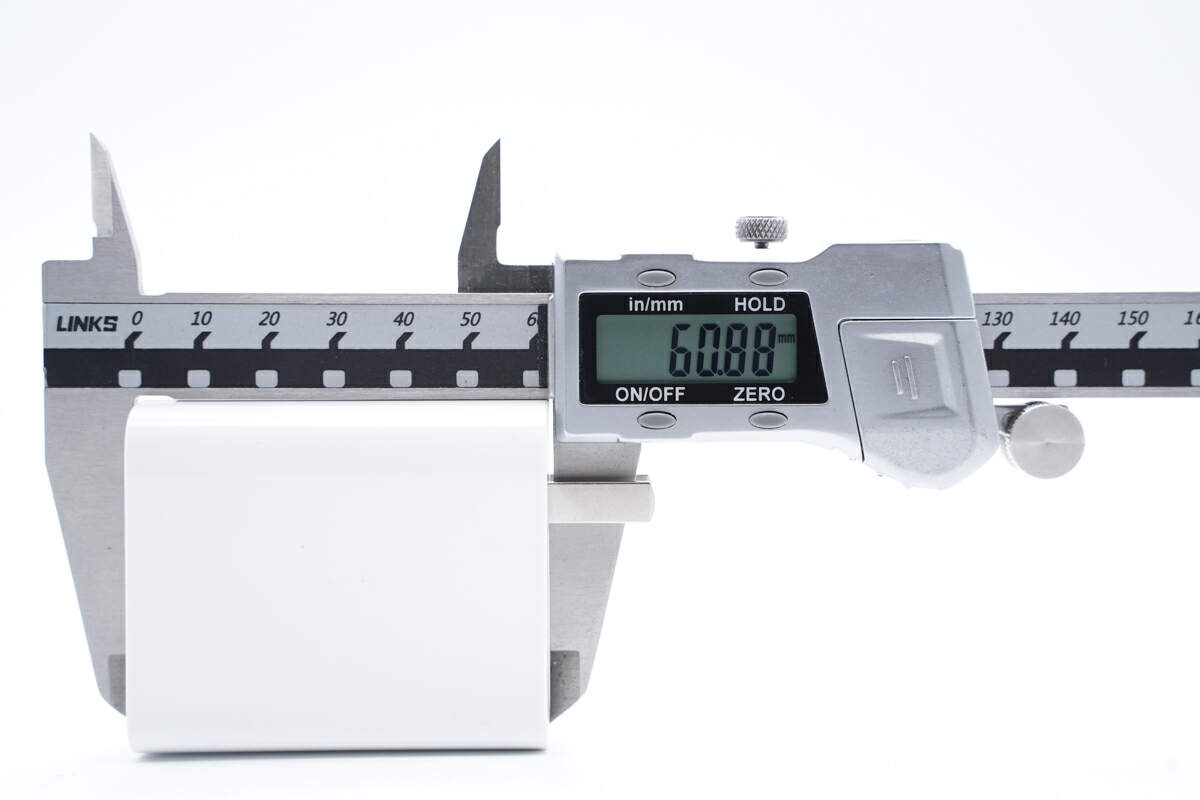
The length of the charger is about 61mm (2.40 inches).
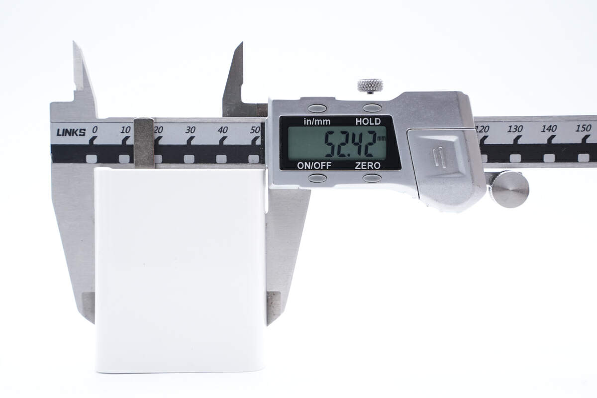
The width is about 52mm (2.05 inches).

And the height is about 29mm (1.14 inches).
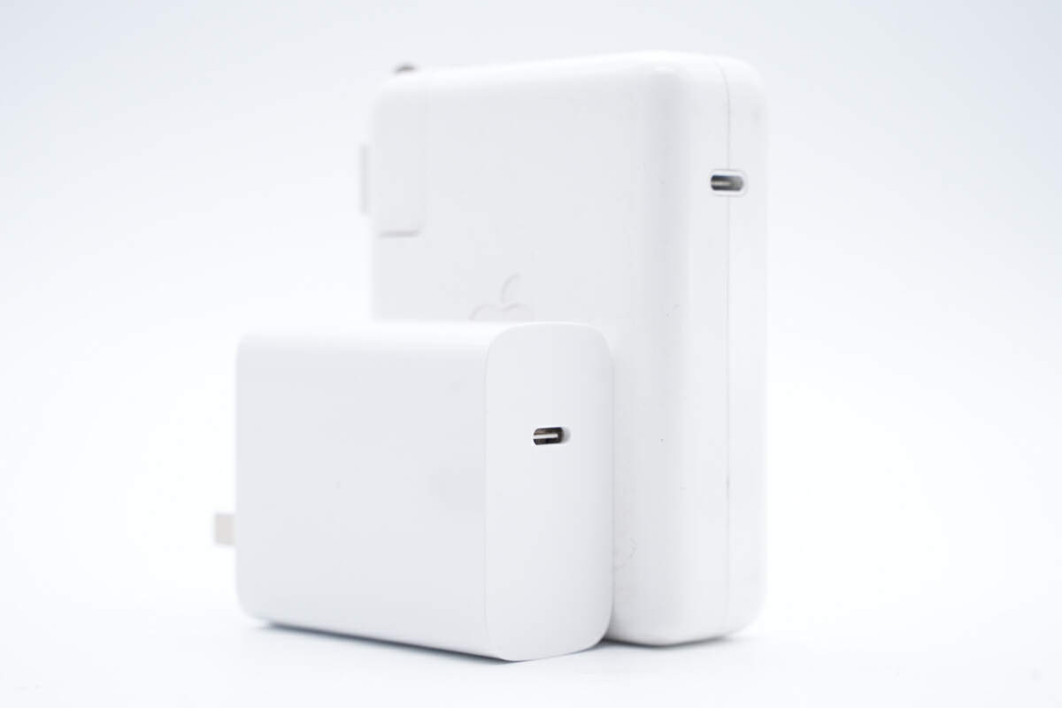
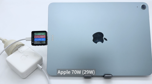
Compared with the Apple 140W charger, the size is almost half of it.
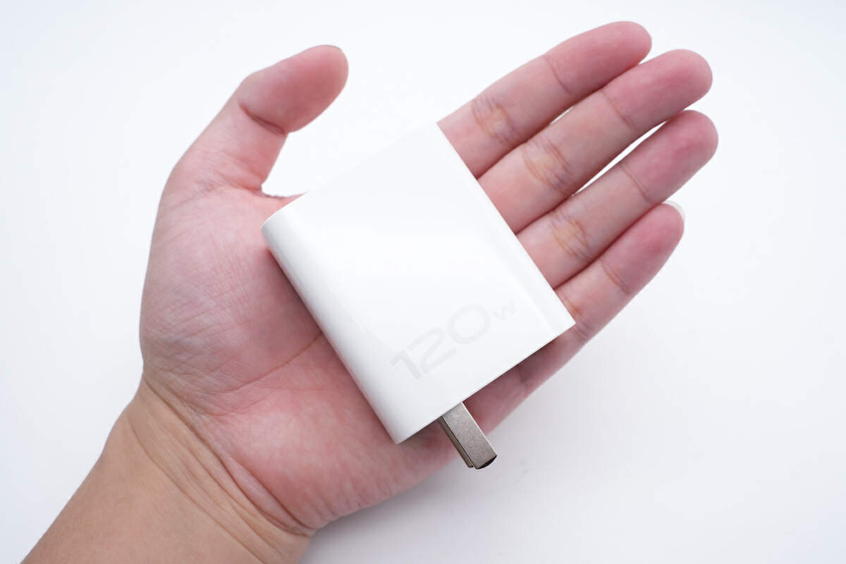
This is how it looks like on my hand.
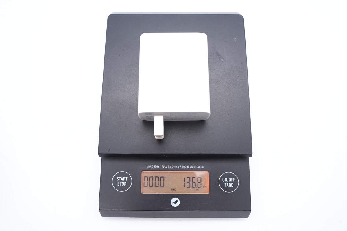
And the weight is about 137g (4.83 oz).
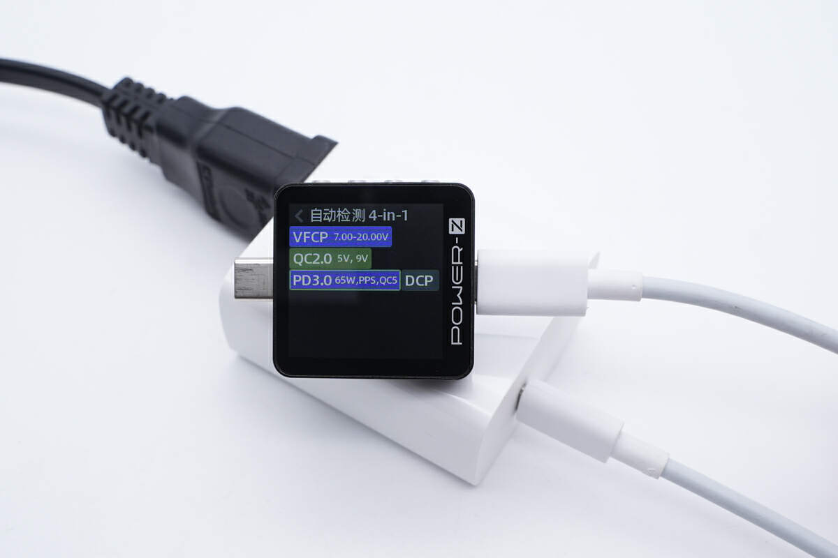
The ChargerLAB POWER-Z KM003C shows it supports vivo flash charge, QC2.0, PD3.0, PPS, QC5, and DCP protocols.
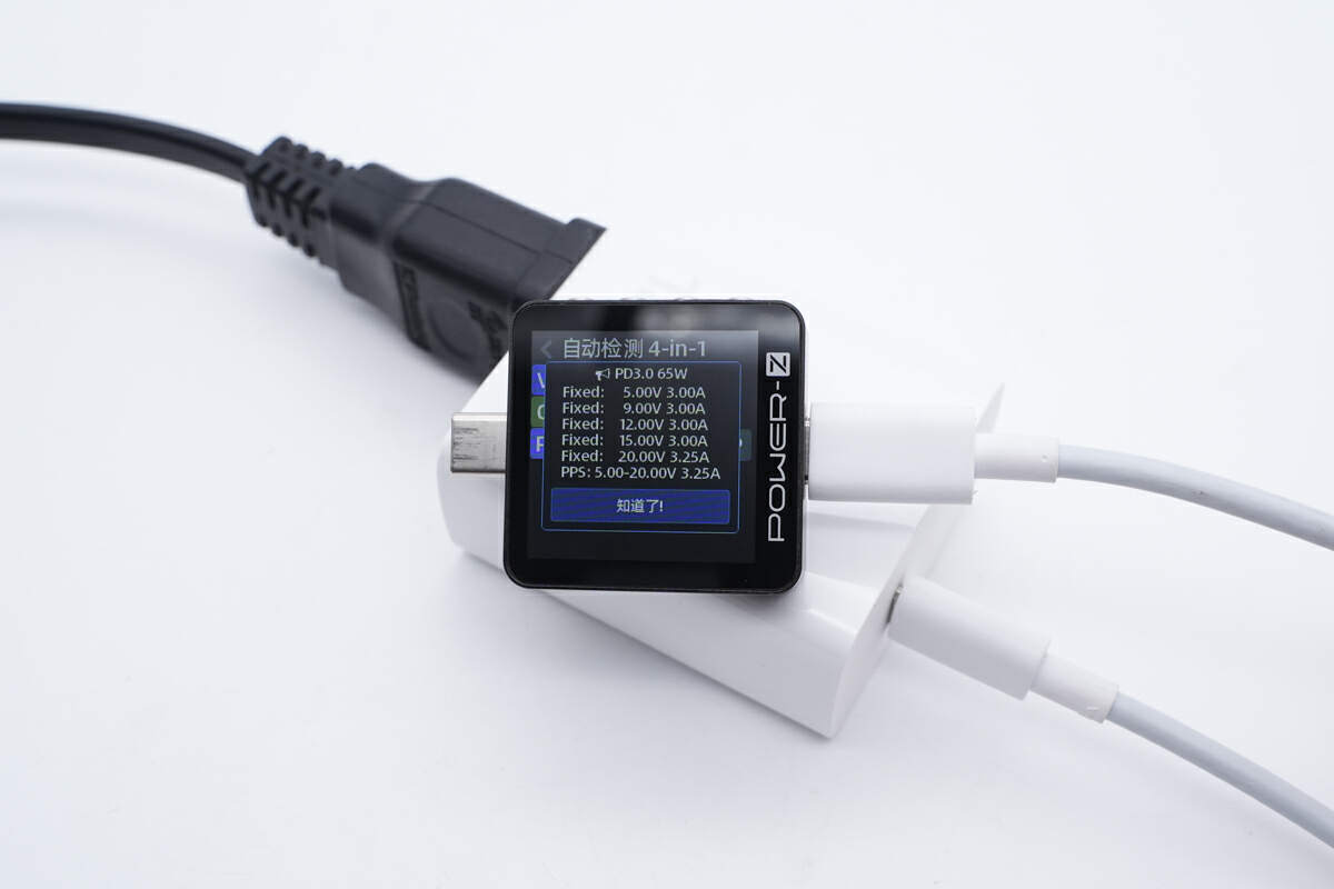
And it also supports five fixed PDOs of 5V/9V/12V/15V 3A, 20V 3.25A, and a set of PPS.
Teardown
Now that we have completed our unboxing and testing of this vivo charger, it's time to take apart the device and examine its internal components and structure.
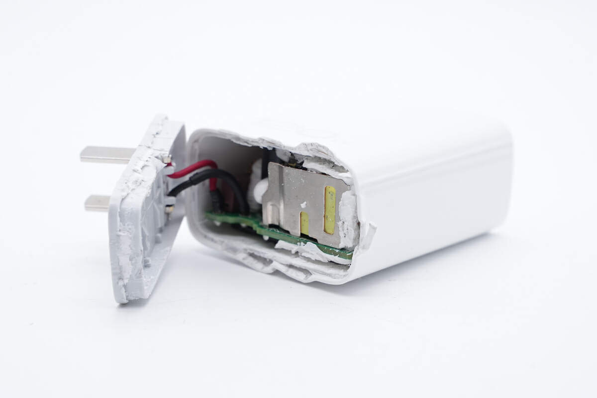
As always, pry along the gap and remove the plastic case of the input side.
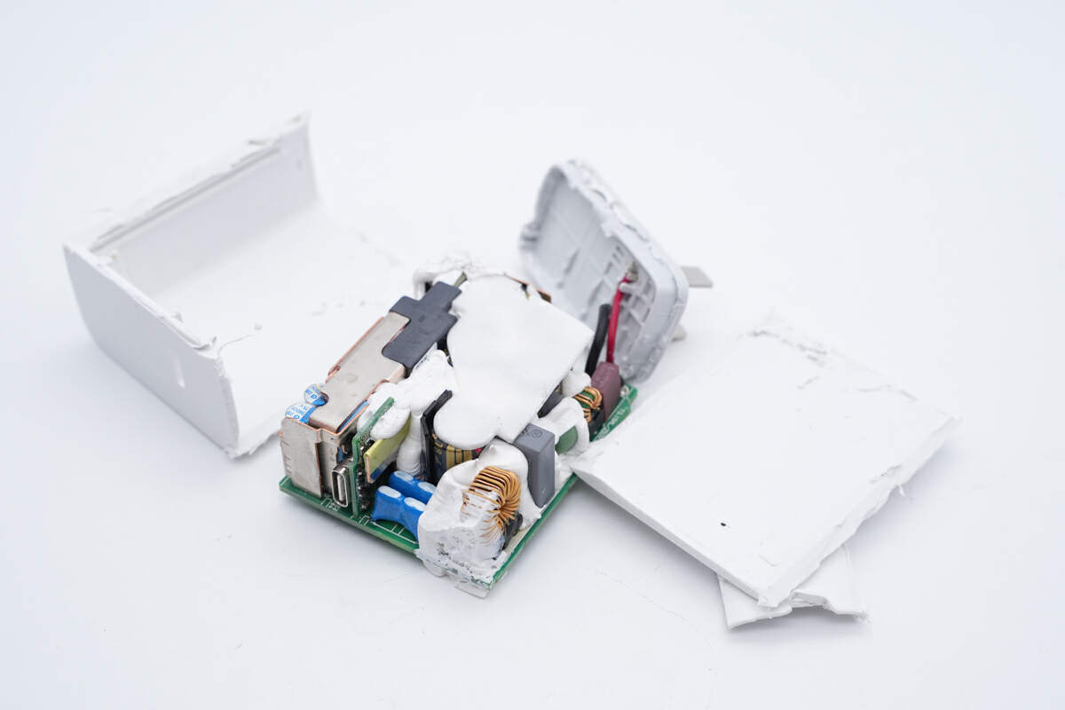
Then, use the cutting machine to cut it off.
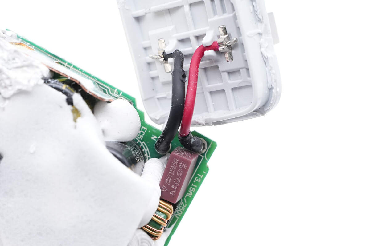
Two input prongs are connected to the main PCB through black and red wires.
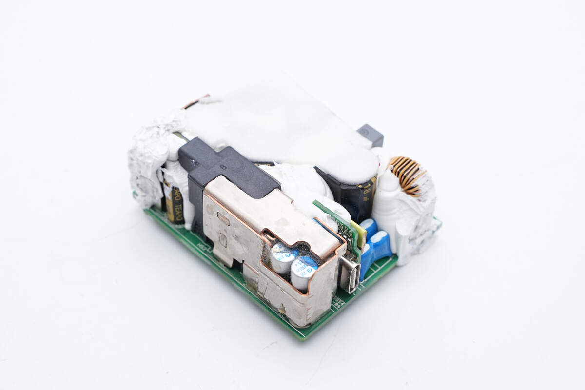
All gaps between components are filled with potting compound for fixing and heat dissipation.
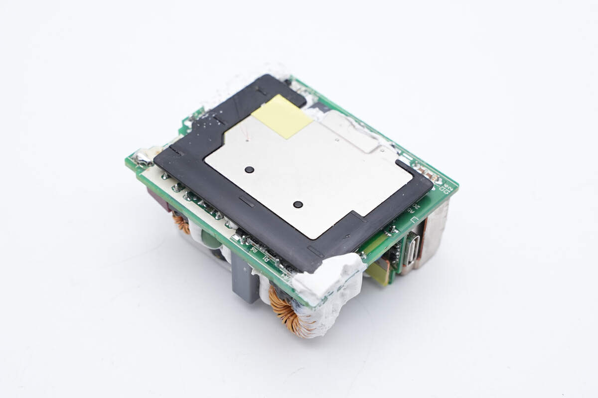
And the back is pasted with a black isolation plate and heat sink.
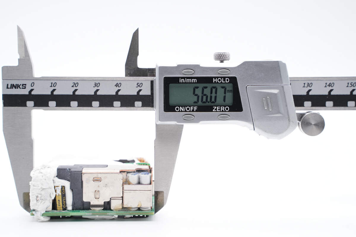
The length of the PCBA is about 56mm (2.20 inches).
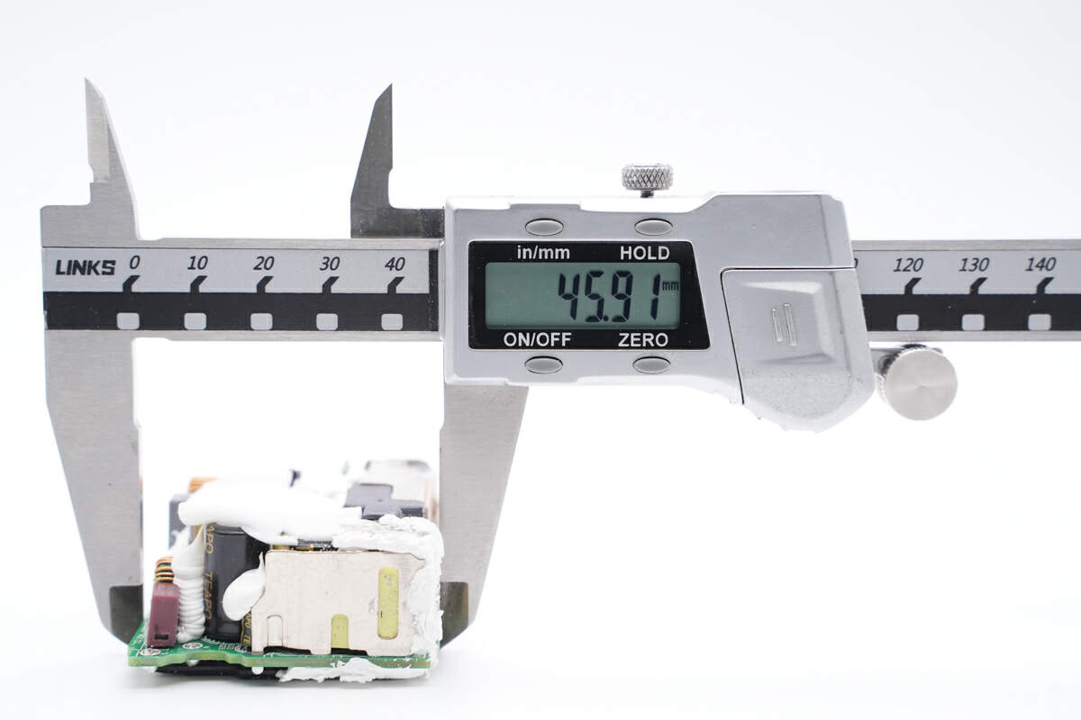
The width is about 46mm (1.81 inches).
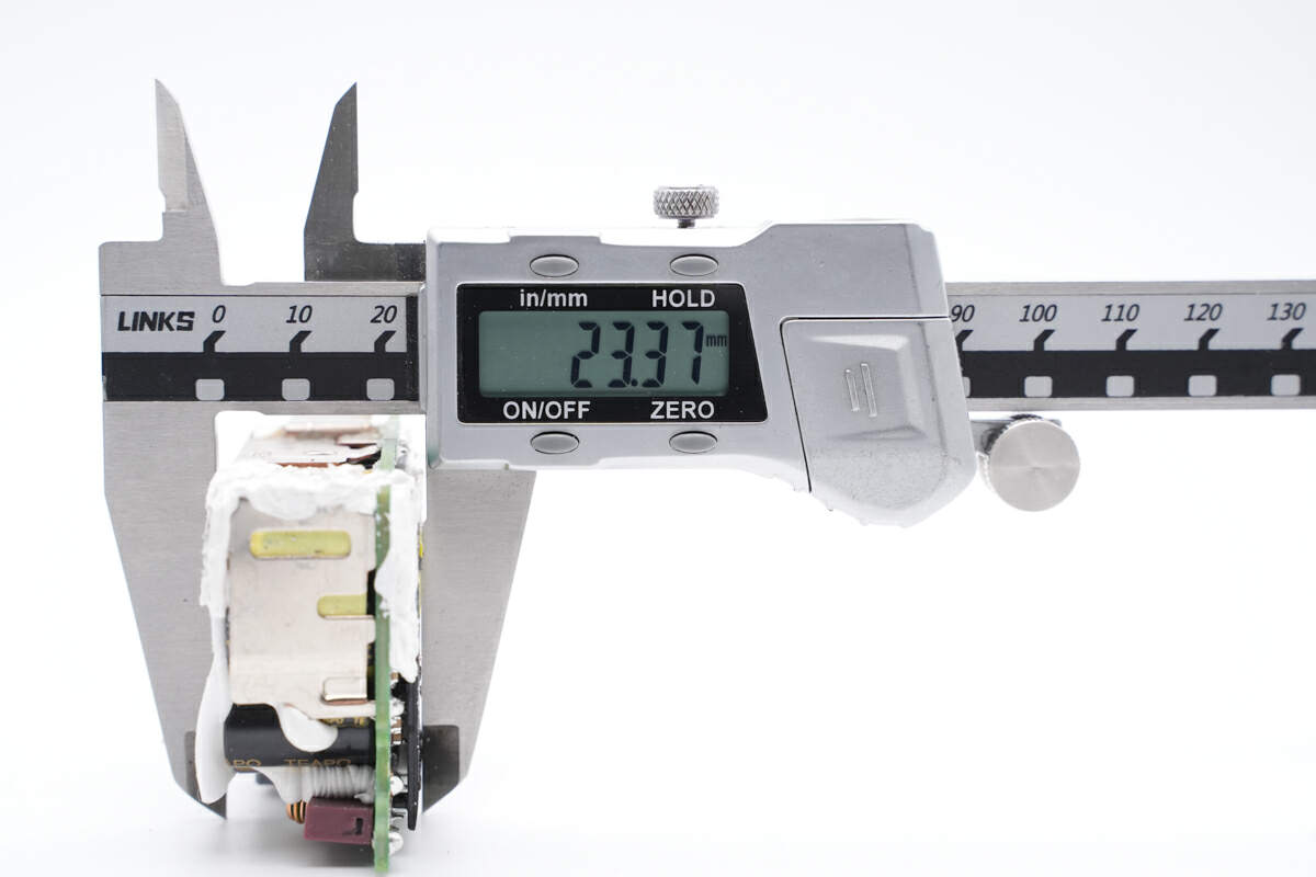
And the height is about 23mm (0.91 inches).
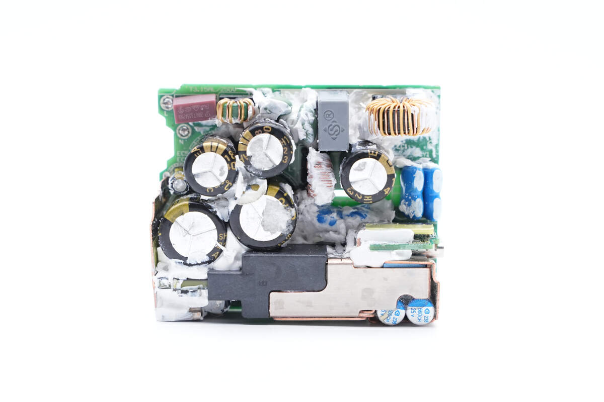
The input fuse, EMI filter circuit, high-voltage filter capacitor, planar transformer, and blue Y capacitor are on the front of the PCBA module.
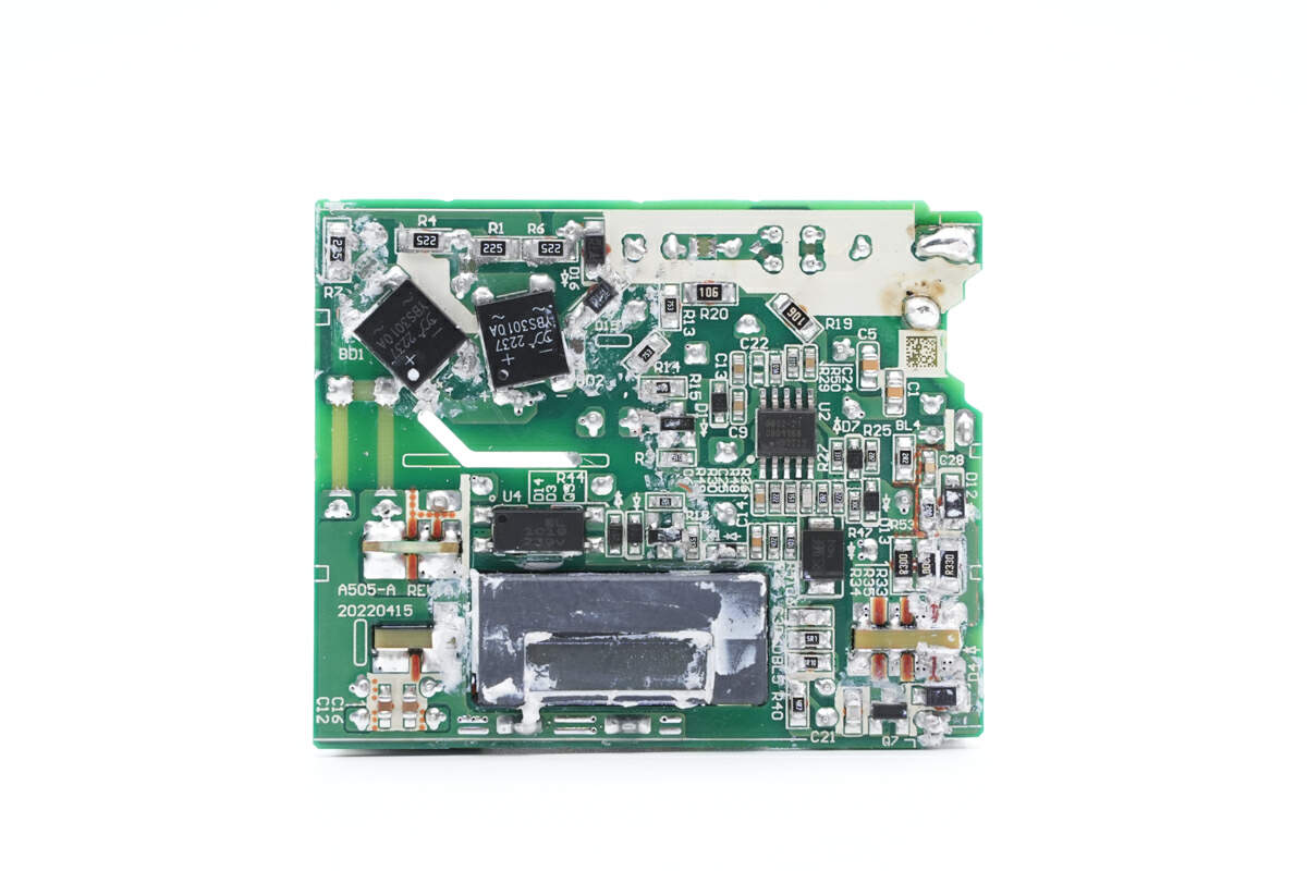
And the bridge rectifier, master controller and the feedback optocoupler are on the back.
After cleaning it up, we found the planar transformer is placed in the hollow of the PCB to reduce the overall thickness.
And it adopts ZVS flyback topology, the protocol chip controls the output voltage through an optocoupler to achieve a wide-range output. Next, we gonna introduce all components inside.

The input time-delay fuse is from WalterFuse. 3.15A 250V.
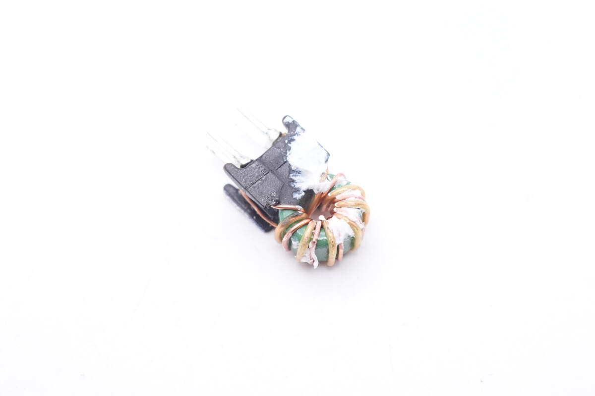
The first common mode choke is wound with magnet wires and insulated wires.
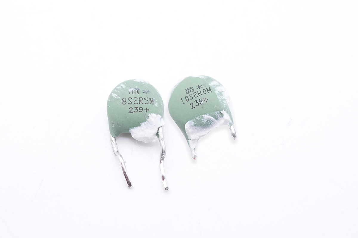
Those two NTC thermistors are used to suppress the inrush current.
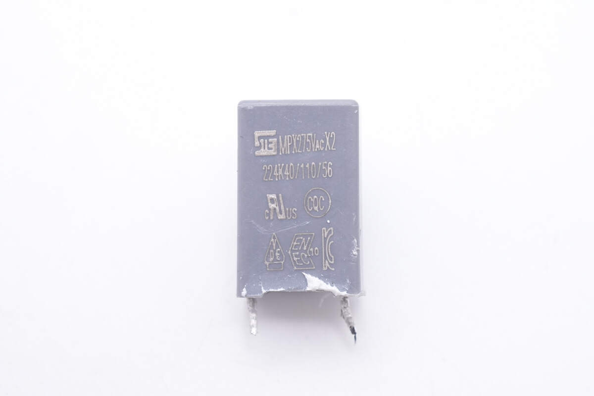
The safety X2 capacitor is from STE. 0.22μF.
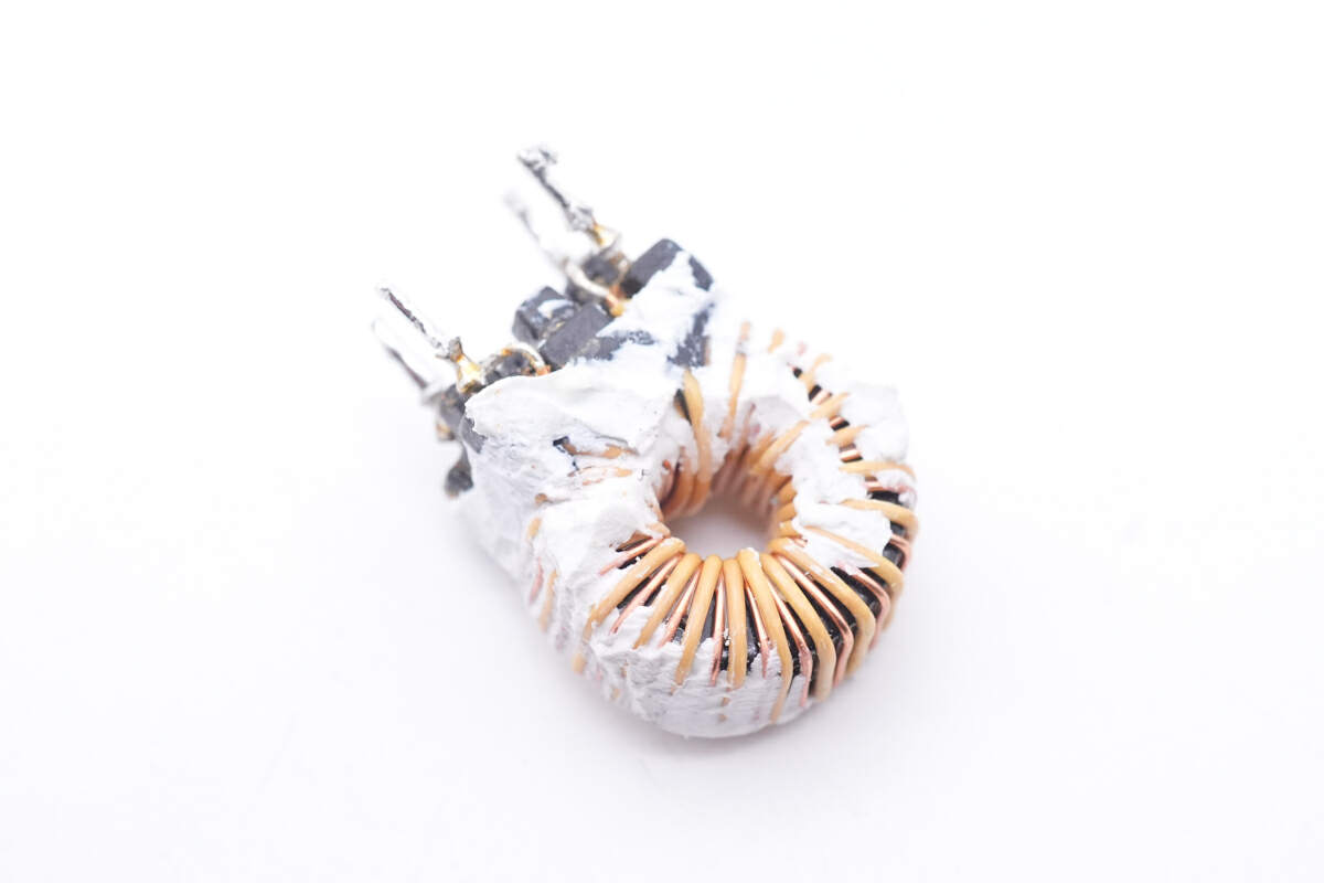
The second common mode choke is actually larger than the first one and is also wound with magnet wires and insulated wires.
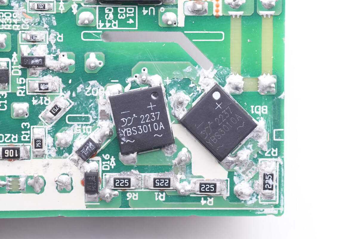
Those two bridge rectifiers are from Yangjie. They're connected in parallel to form a half-bridge circuit and dissipate heat evenly. Model is YBS3010A. 3A 1000V.
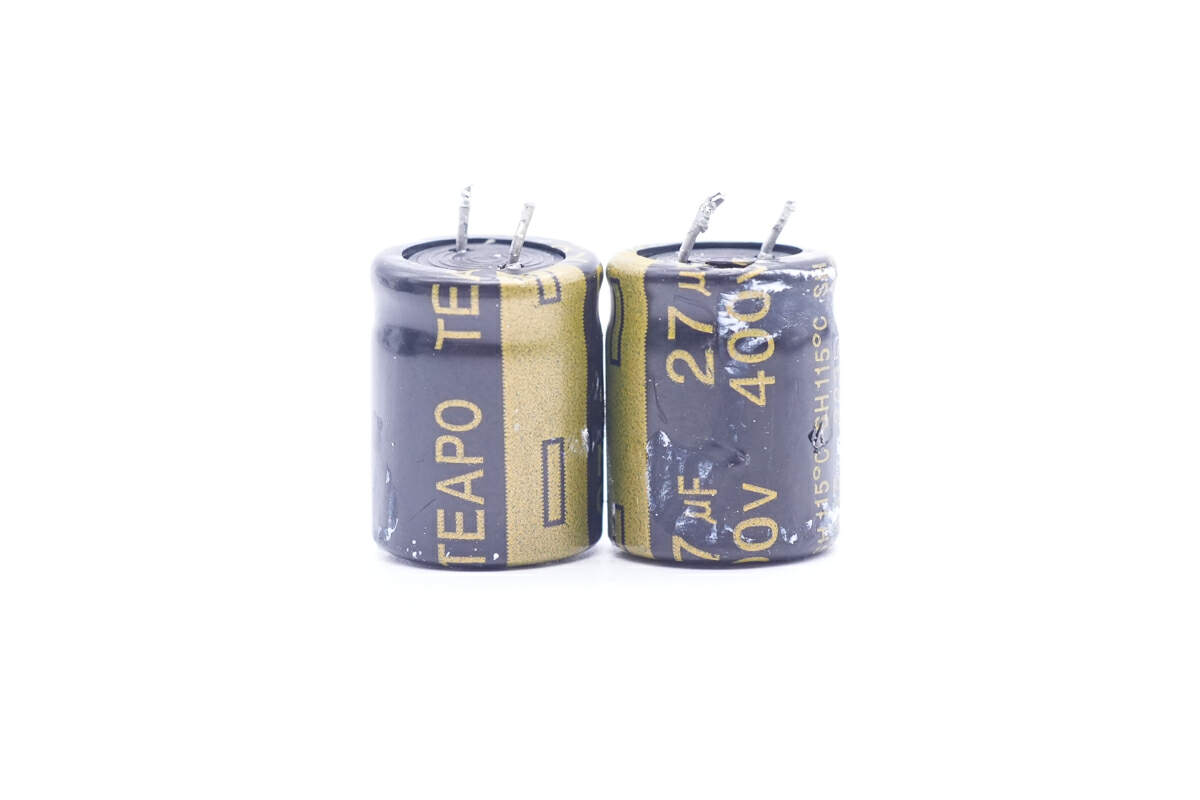
These two capacitors are from TEAPO, 27μF 400V for each.
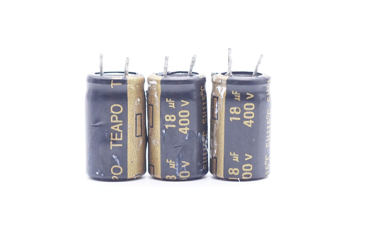
And these three smaller capacitors are also from TEAPO, 18μF 400V for each, 108μF in total.
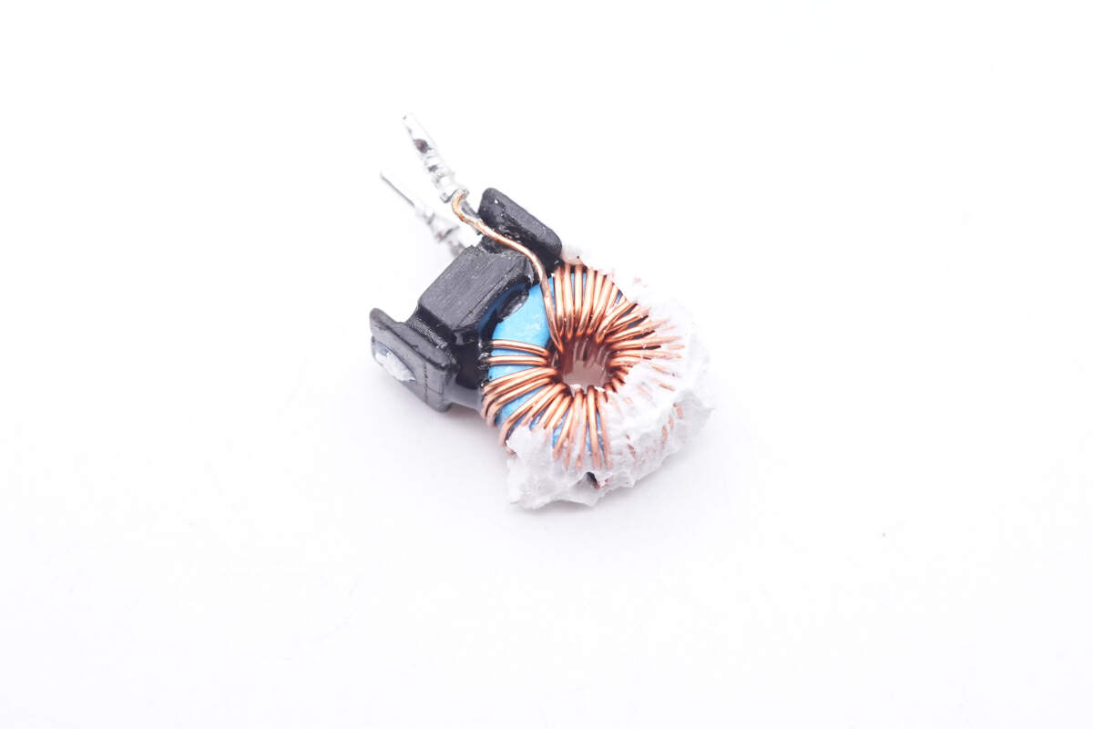
The differential common mode choke is wound with magnet wires.
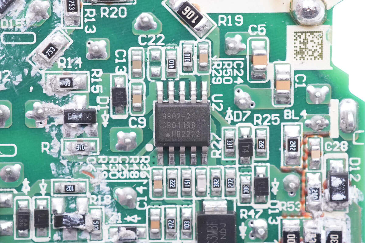
The master controller is from Dialog iW9802, which is a high-performance AC/DC primary-side digital flyback controller with advanced zero voltage switching (ZVS) and adaptive multi-mode-control (MMC) working with secondary-side regulation (SSR) for applications requiring high power density and high resolution in output voltage/current setting.
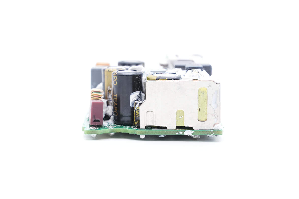
There's another heat sink located in here.
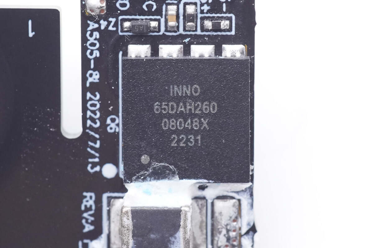
The GaN FET is from Innoscience, model INN650DAH260, which is a customized model and has the same spec as the INN650D260A. It's qualified to JEDEC standard and supports ESD protection. 650V 260mΩ.
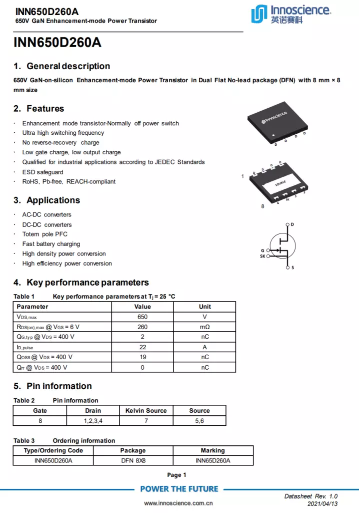
Here is all the information about Innoscience INN650DAH260A.
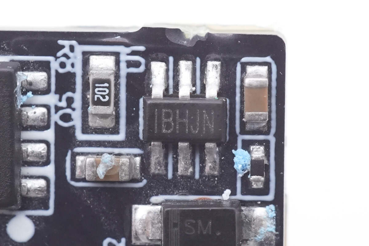
The secondary synchronous rectification controller marked with IBHJ is from MPS, model is MP6908A, and the maximum operating frequency is 600KHz. It can support multiple working modes such as DCM, CCM, Quasi-Resonant Operations and Active Clamp Flyback, no need for auxiliary winding high-side or low-side rectification, have ringing detection to prevent false turn-on, and support logic voltage and standard voltage synchronous rectifiers.
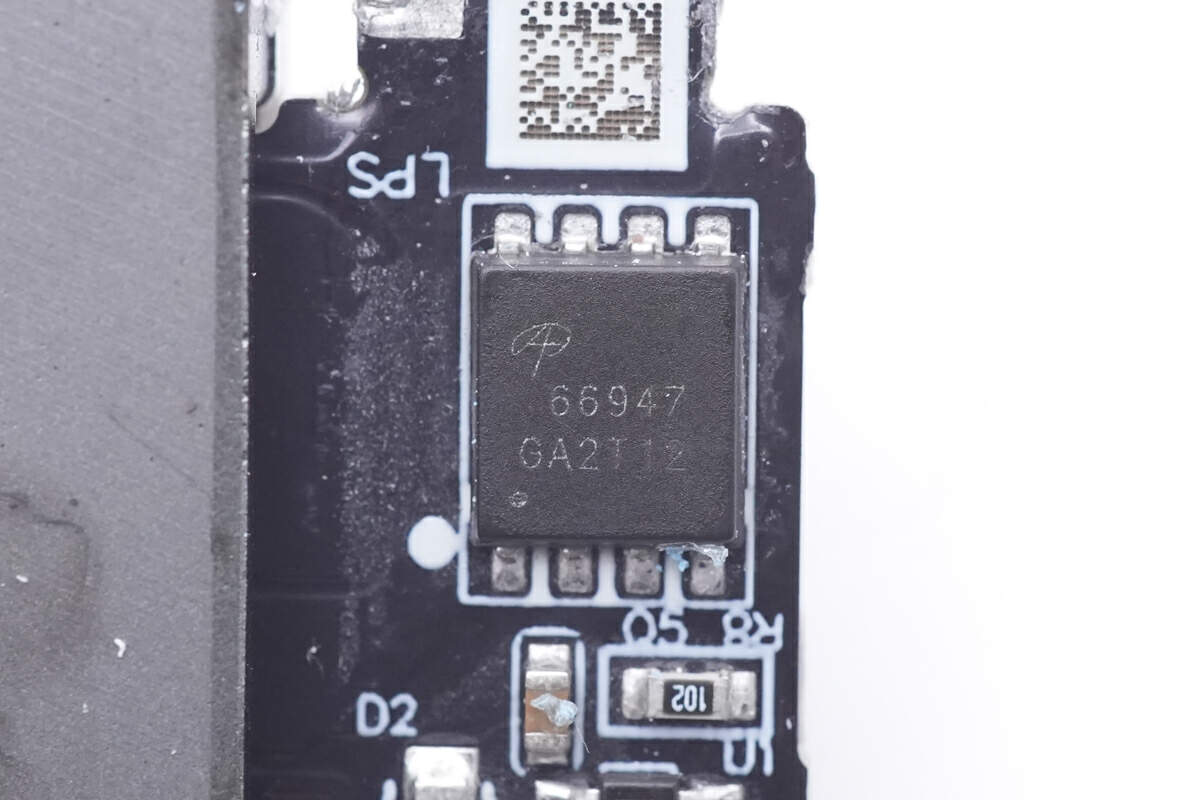
The synchronous rectifier marked with 66947 is from AOS and adopts DFN5 x 6 package.
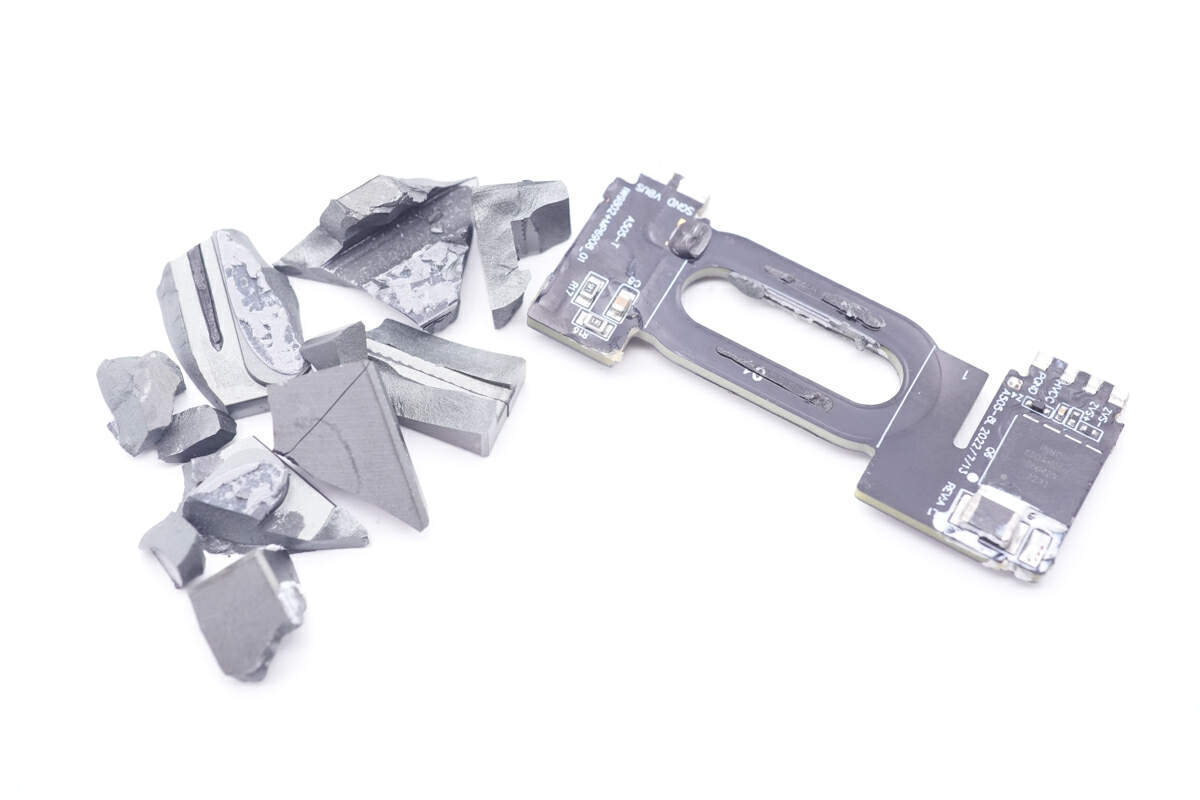
Smashing the ferrite core of the planar transformer.
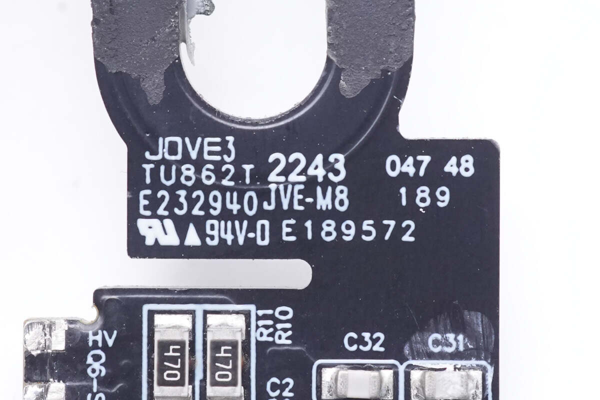
The planar transformer's small PCB is from JOVE.
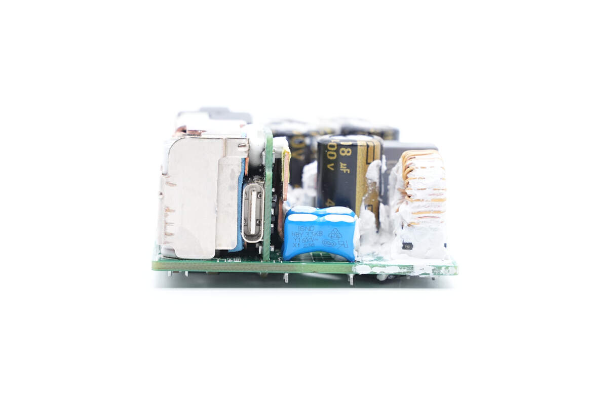
The solid capacitor for output filtering, small output PCB, blue Y capacitor and common mode choke are on the output end.
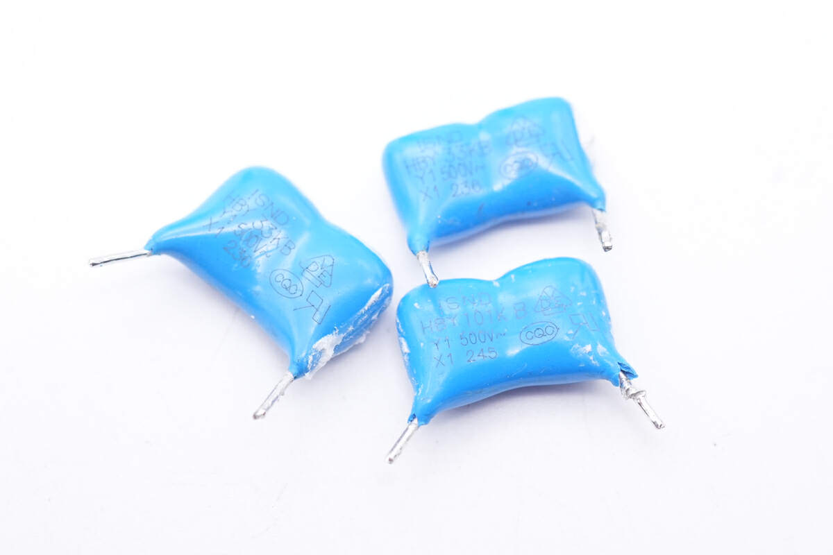
Those three Y capacitors are from ISND, which are connected in series.
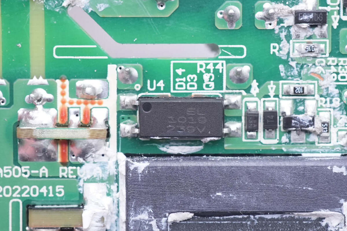
The EL1019 optocoupler is above the planar transformer, which regulates the output voltage.
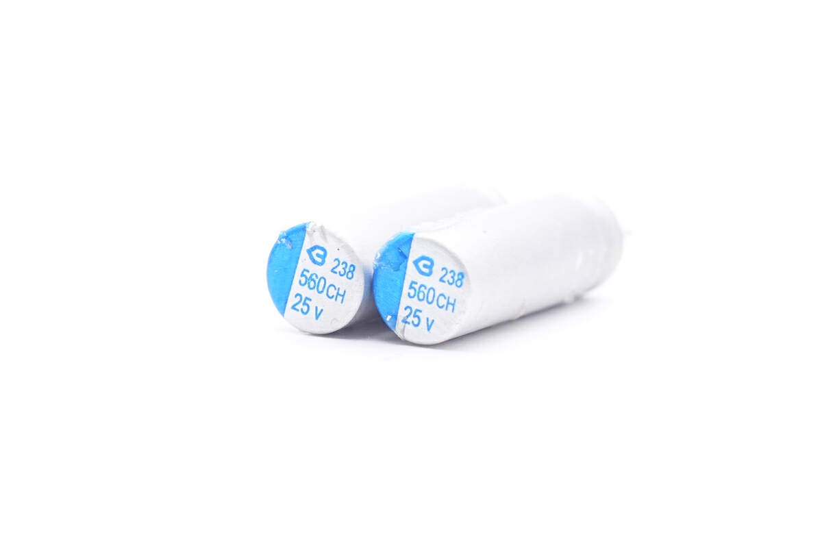
Those two solid capacitors for output filtering are from Beryl, they're connected in parallel. 560μF 25V.
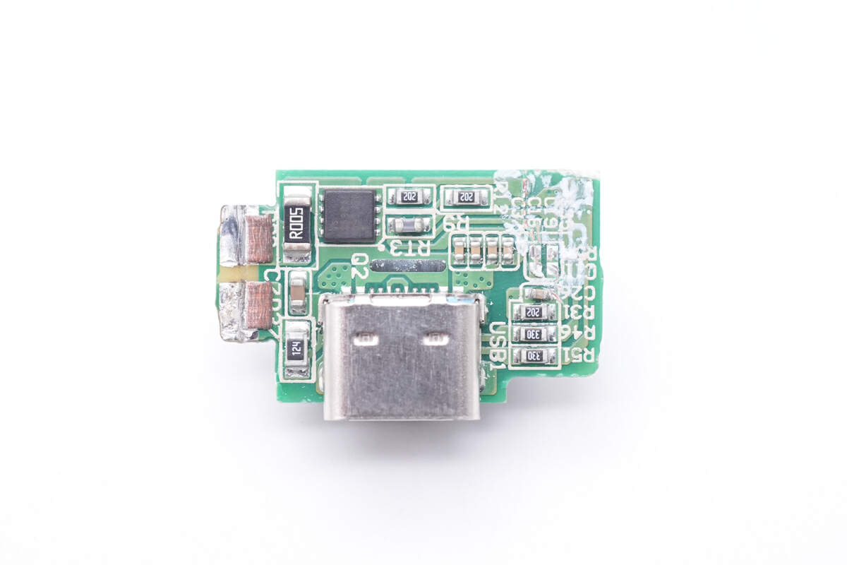
The current sampling resistor, VBUS MOSFET and USB-C socket are on the front of the small output PCB.
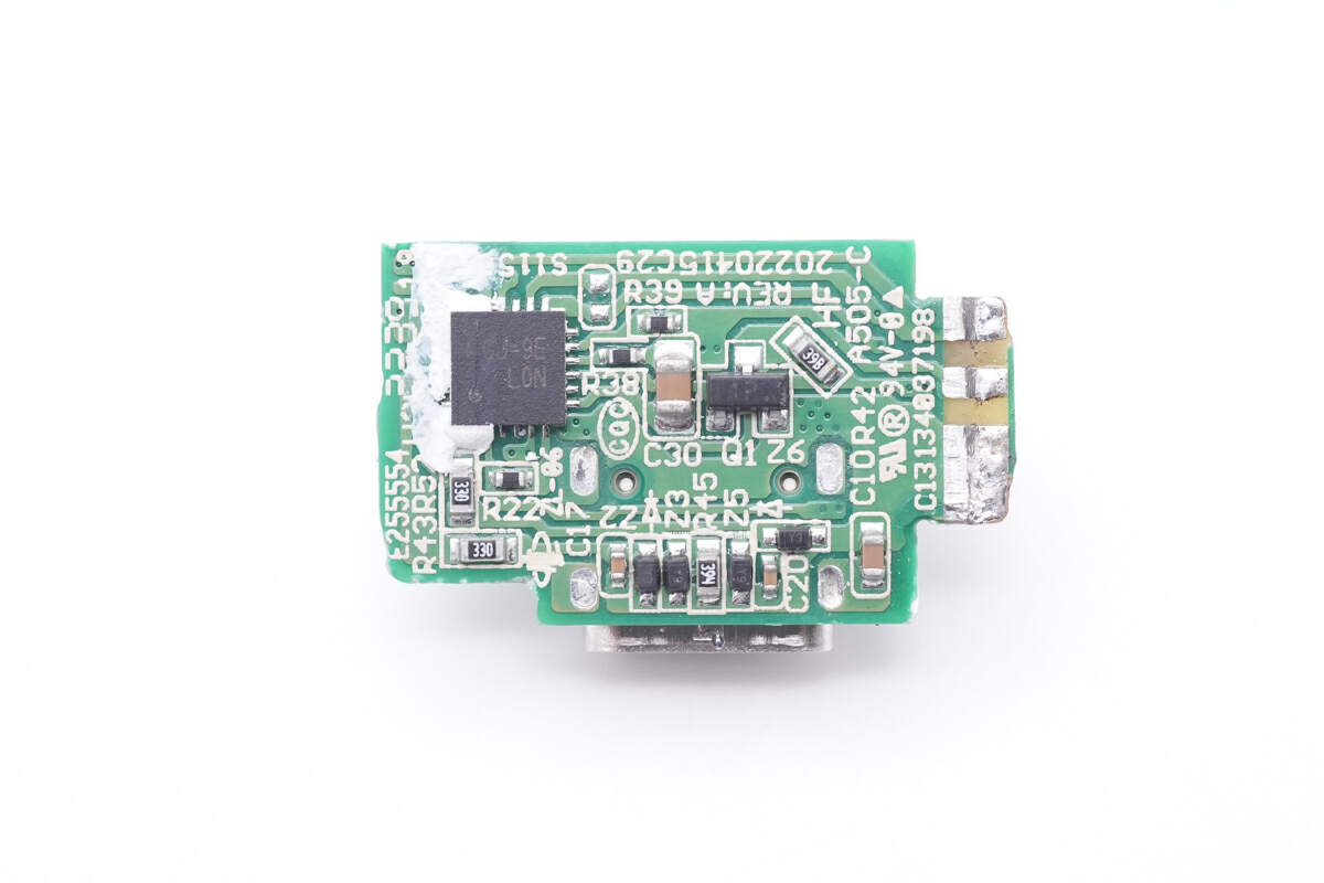
And the protocol chip and some other components are on the back.
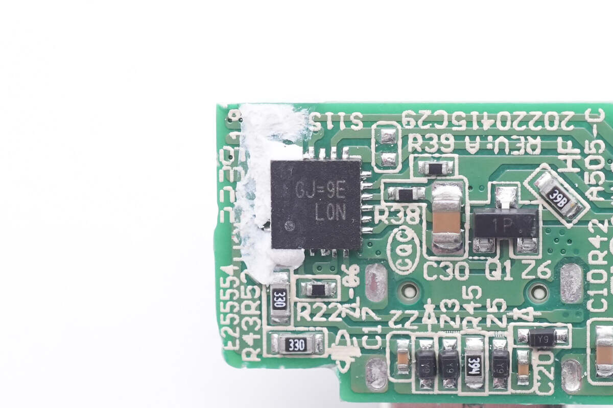
The protocol chip marked with GJ=9E is from Richtek.
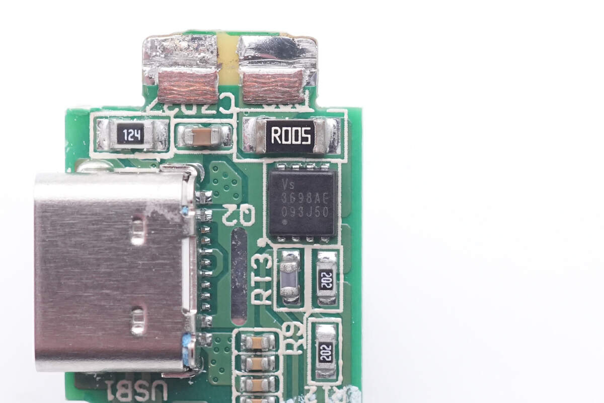
The output VBUS MOSFET is from Vergiga Semi and adopts PDFN3333 package. Model is VS3698AE. 30V 3mΩ.
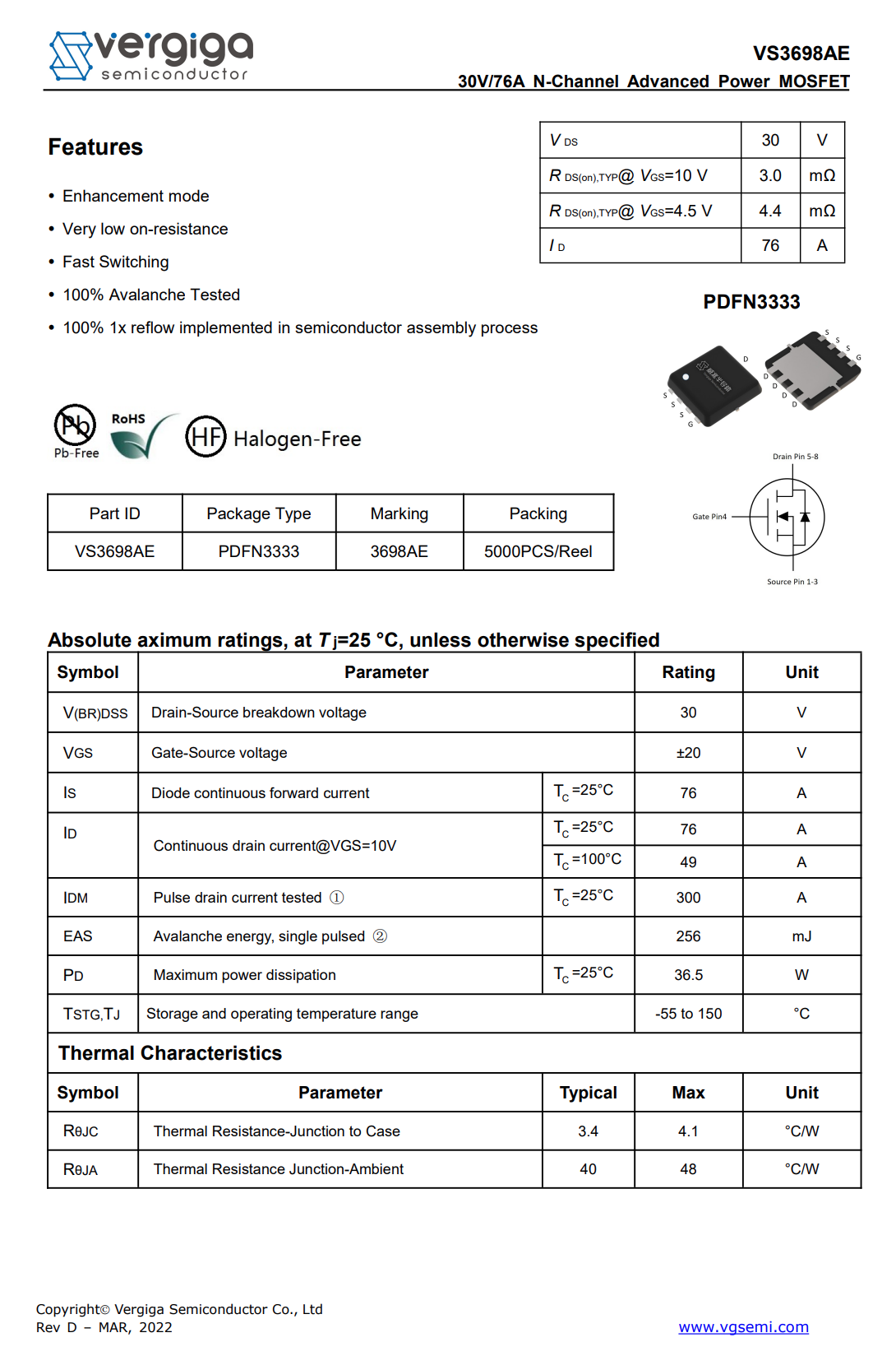
Here is all the information about Vergiga Semi VS3698AE.
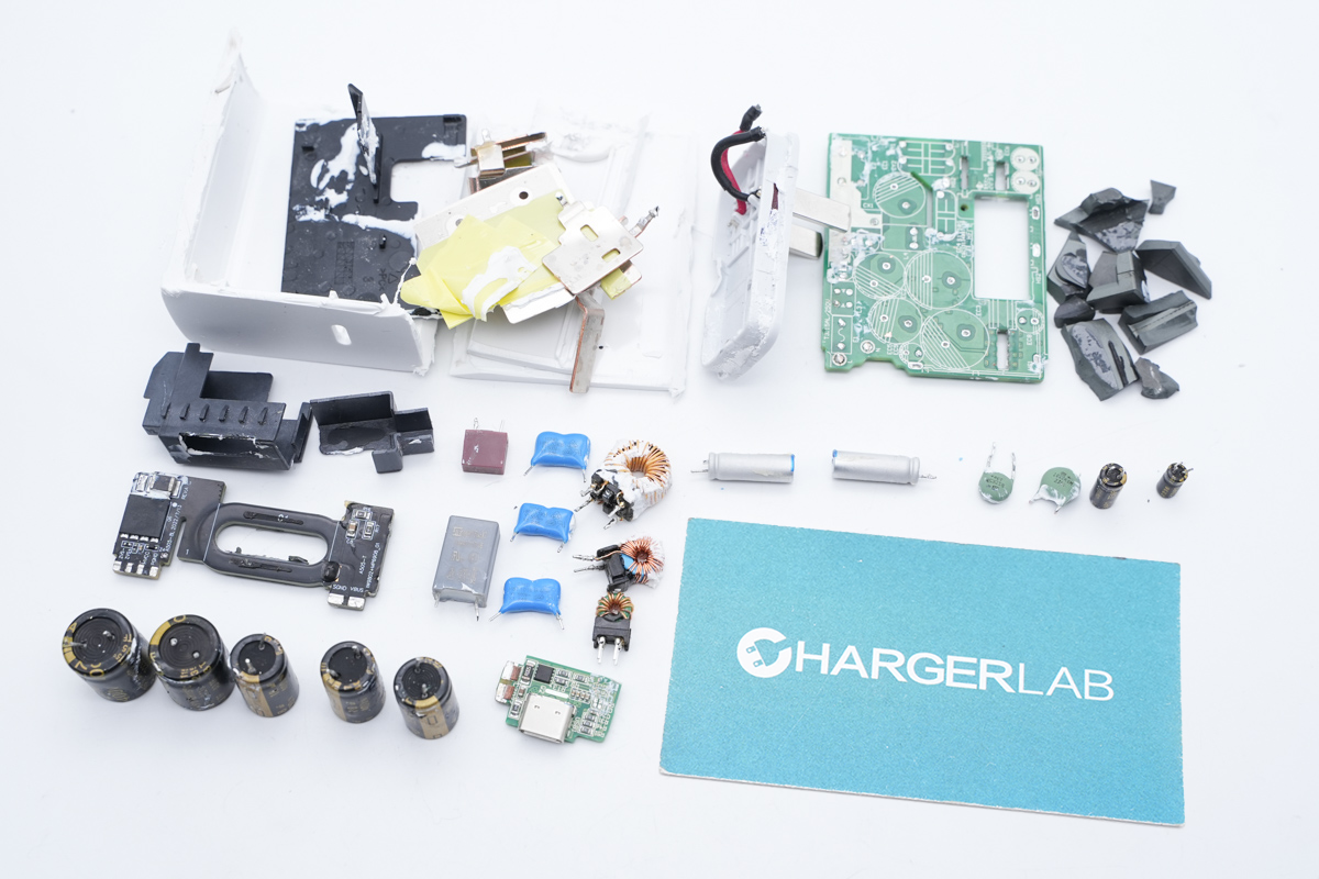
One last look at all the components of this vivo 120W flash charge GaN charger.
Summary of ChargerLAB
The 120W flash charge GaN charger that comes with Vivo smartphones has a stylish, flat white exterior design, making it sleek and modern in appearance. Its compact size and fixed input prongs design make it pretty sturdy and easy to use. Additionally, the charger is designed with a single USB-C port and has a 65W PD fast charging output, which can not only meet the high-power charging needs of smartphones but also provide charging capacity for laptops. With this versatile and powerful charger, Vivo users can easily charge all their devices with just one convenient accessory.
After taking it apart, we found that it adopts a planar transformer and GaN FET inside, which is the critical component to make it compact. The GaN FET is from Innoscience, and it's a customized model for this charger with high quality.
Related Articles:
1. Teardown of vivo/IQOO 120W Flash Charge GaN Charger (Video)
2. Teardown of iQOO 200W GaN Charger (For iQOO 10 Pro)
3. Teardown of vivo 80W Flash Charge Charger (Dual USB-C)

