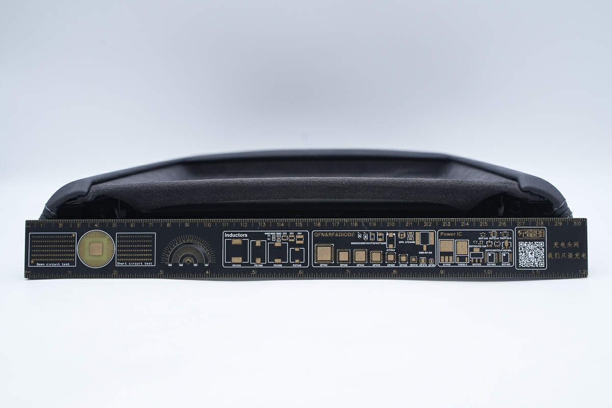
Introduction
ChargerLAB got the wireless phone charger WC5 for the Tesla Model 3. The surface of this wireless charging module is covered with flocking material, which is soft and non-slip. There are two charging positions that support 15W wireless charging. It uses an aluminum alloy shell to enhance heat dissipation. The tilted angle of its charging panel makes it easy to place and view the phone, improving driving safety. The wireless charging module is integrated with the vehicle interior and looks beautiful. Next, let's take it apart to see its internal components and structure.
Product Appearance

The Tesla wireless phone charger is dark gray, with leather edges and flocking material in the middle.

The overall shape is an inverted trapezoid.
Close-up of the flocked panel.

Close-up of the bump used to locate the phone.

There are fixing screws on both sides and the middle of the aluminum alloy shell.
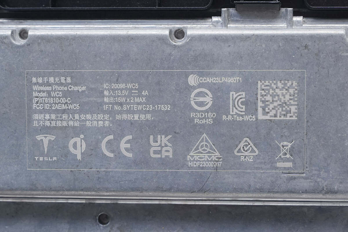
Model is WC5. It can support input of 13.5V 4A. The maximum output is 15W, respectively.

Close-up of the opening used to secure the aluminum alloy shell.

There are also clips to fix the aluminum alloy shell.

The aluminum alloy shell is fixed by screws.

Close-up of the connector used to connect to the vehicle's power supply.

The panel is internally joined by heat fusion.
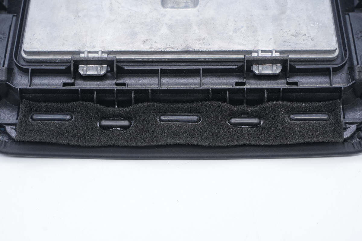
The bottom is equipped with sealed foam.

There are tonal stitching on the sides.
The top width is about 30 cm (11.81 inches).

The height is about 23.3 cm (9.17 inches).

That's how big it is in the hand.

The weight is about 766.6 g (27.041 oz).
Teardown
Next, let's take it apart to see its internal components and structure.

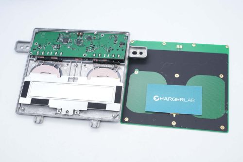
First, unscrew the fixing screws of the aluminum alloy shell and remove the panel.

The shielding plate is fixed by stamping, and there is an NFC coil in the area corresponding to the wireless charging.

The shield plate is printed with TESLA.
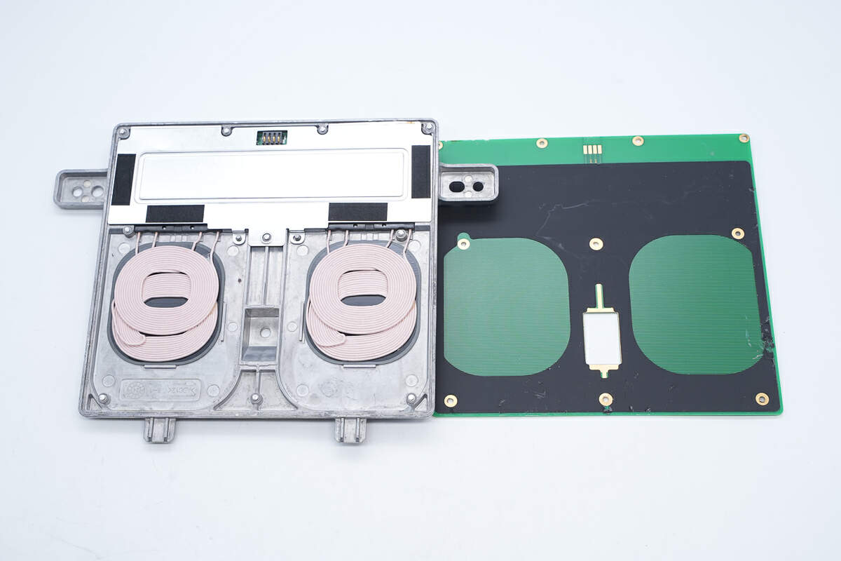
Remove the shielding plate, there is a metal shielding cover and wireless charging coils inside.

There is cushioning foam and NFC coil contacts on the back of the shield.

The metal shielding cover has a hole to expose the NFC coil contacts.

Buffer foam is arranged inside the shielding cover and the shielding plate.

Remove the shielding cover and the PCBA module is fixed with screws.
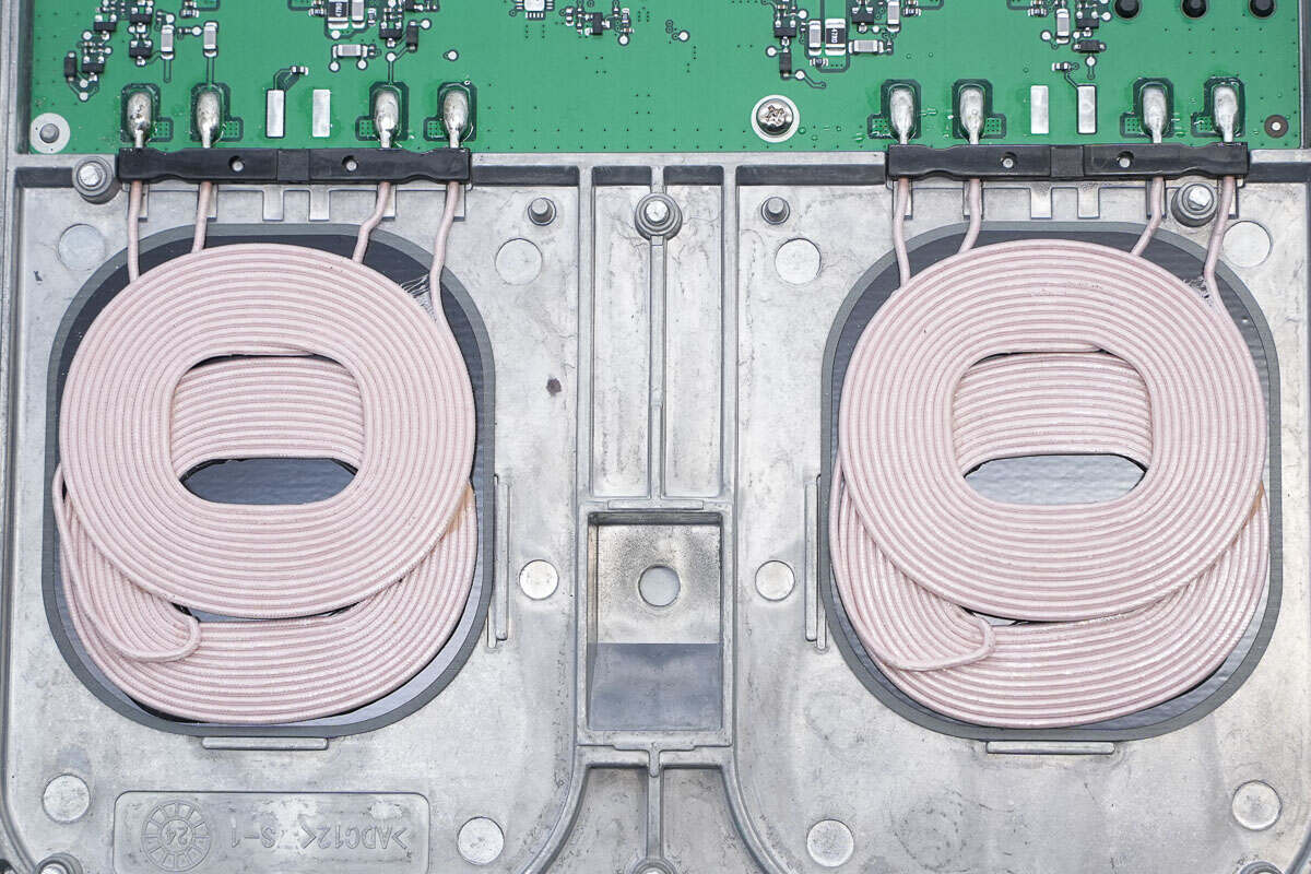
There are two wireless charging coils on the left and right.

Each charging position has two coils stacked together to increase the charging area.

The welding points of the wireless charging coil are full and round.

The leads of the coil are fixed by a plastic bracket.

The PCBA module is fixed with screws.

Unscrew the fixing screws of the PCBA module.

There are pink potting compounds at the location of the heat-generating components, which dissipate heat through the aluminum alloy shell.
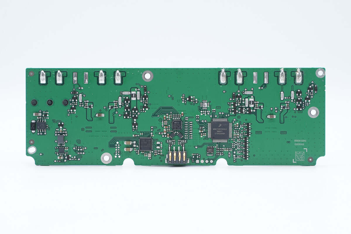
One side of the PCBA module is soldered with the wireless charging master control chip, NFC communication chip, MCU, and LIN and CAN communication chip.

The other side of the PCBA module has a power socket, a synchronous buck converter, two wireless charging power stage chips, a buck inductor, and a filter capacitor.

This is the power supply connector.

The input TVS marked with CK is from BrightKing and adopts DO-214AA package. It is a bidirectional TVS with a reverse cutoff voltage of 30V. Model is SMBJ30CA.
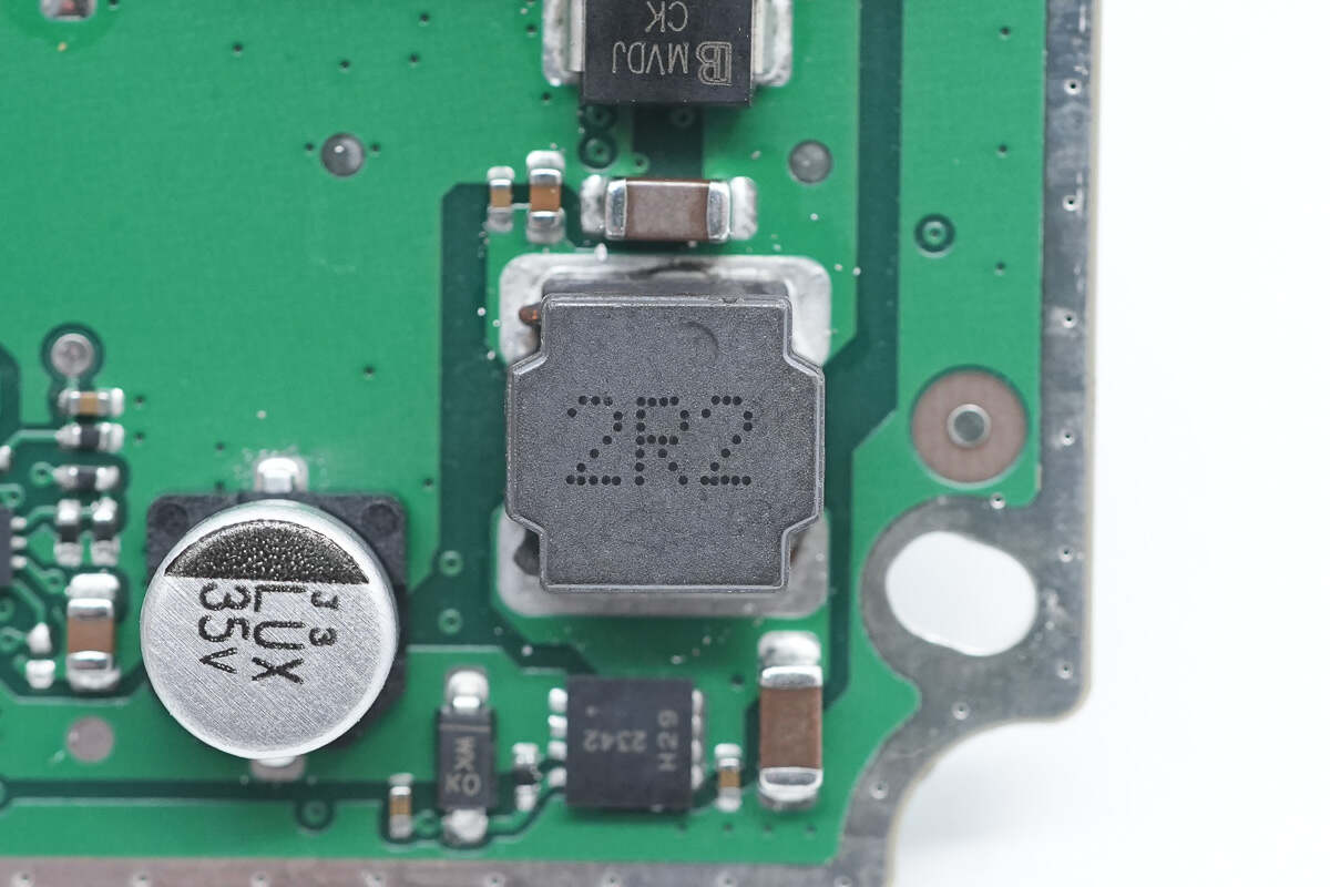
This is the filter inductor. 2.2μH.

The MOSFET for power input isolation is from DIODES and marked with H29. It has a withstand voltage of -40V, a resistance of 18mΩ, an operating temperature of 175°C, and meets the AEC-Q101 standard. It adopts PowerDI3333-8 package. Model is DMPH4029LFGQ.

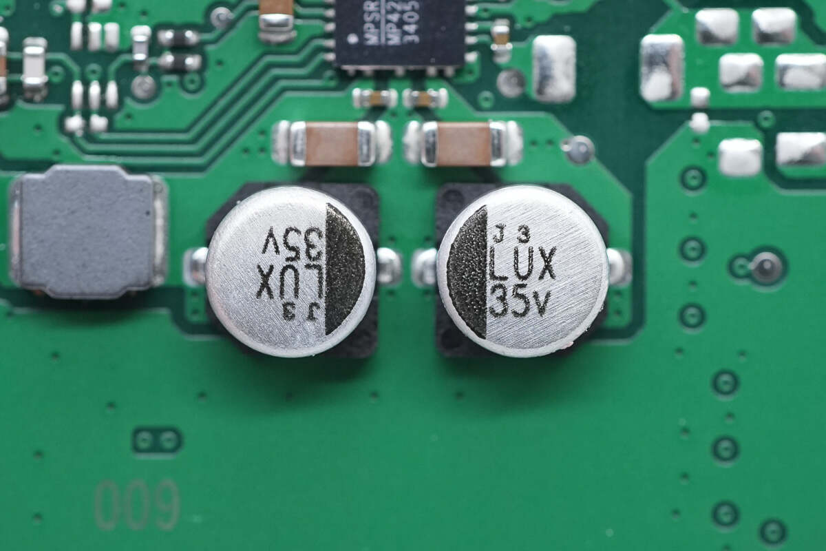
There is the filter capacitor. 35V.

The step-down chip marked with 4215FA is from TI and adopts VQFN-HR package. It is an automotive-grade synchronous buck converter that meets the AEC-Q100 standard, supports -40~125℃ ambient temperature, and has an internal integrated MOSFET. 42V 1.5A. Model is LMR34215FA.

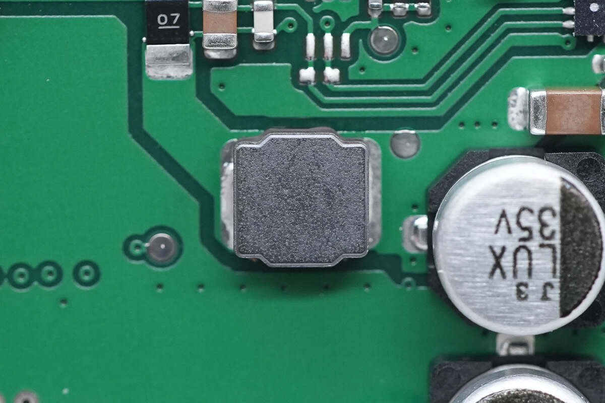
This is the alloy inductor used with it. 10μH.
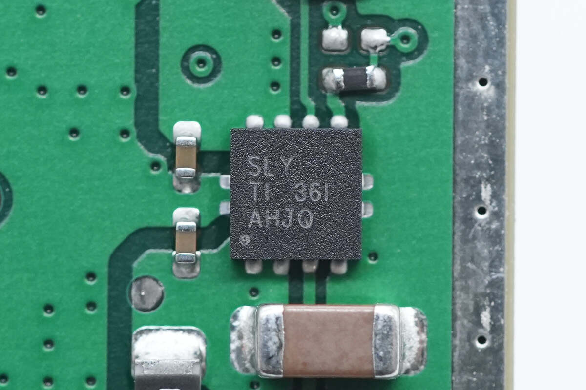
The voltage regulator chip marked with SLY is from TI and adopts SON-8 package. It supports 1A output current and meets AEC-Q100 standard. Model is TPS7A8101-Q1.

The wireless charging controller is from NXP and adopts LQFP64 package. It complies with the AEC-Q100 standard, has two built-in digital demodulation modules, supports wireless charging of two mobile phones at the same time, and has CAN FD/I2C/SCI/SPI interfaces. Model is MWCT22C3AVLH.

This is an external SMD clock crystal.

The synchronous buck chip is from MPS and adopts QFN-21 package. It is a dual-channel synchronous buck converter. The chip supports 36V input voltage and dual 3A output. The output voltage can be configured by the I2C interface. It has output overvoltage protection and overheating protection and meets the AEC-Q100 standard. Model is MPQ4272.

There are six MLCC capacitors around the chip for filtering.

There is an alloy inductor. 4.7μH.

These are the two input filtering capacitors.

The wireless charging power stage chip is from MPS and adopts QFN-22 package. It is used for automotive wireless charging transmitter applications, with an internal low-on-resistance full bridge, a high-precision current sampling amplifier, and a high-voltage buck converter. The current sampling amplifier is used for input power sampling, and the built-in converter can power the wireless charging master. It supports an overheat protection function. Model is MPQ4280.

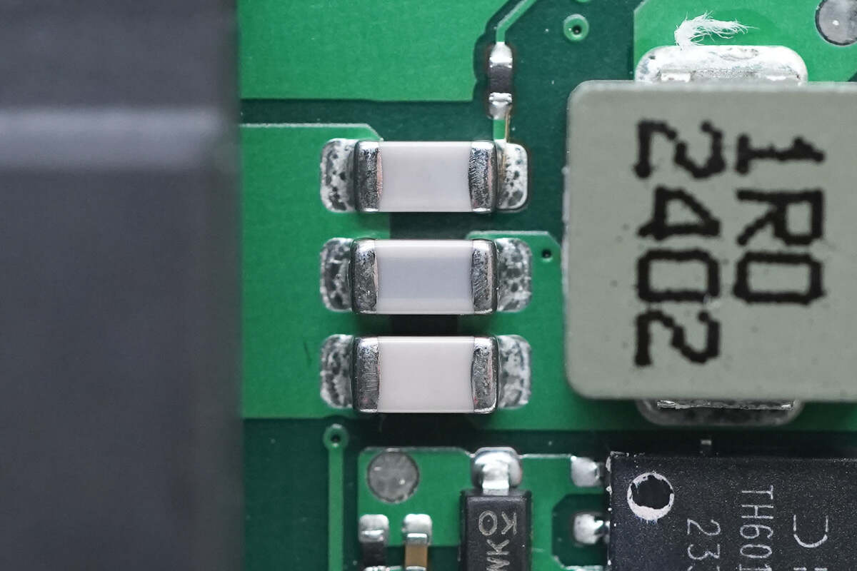
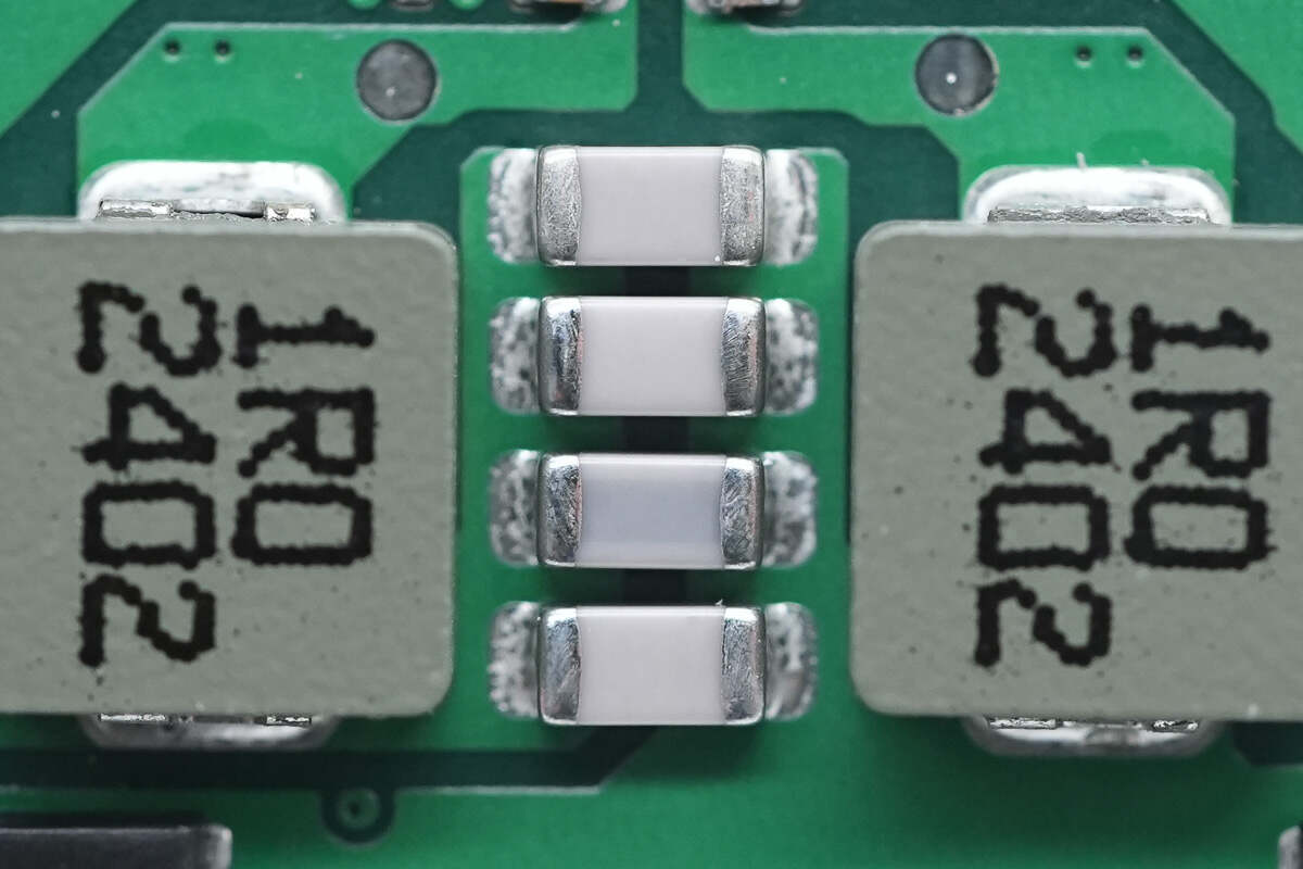
These two 1μH alloy inductors are used for output filtering.

These are four NPO resonant capacitors connected in parallel.
These are three white NPO resonant capacitors.
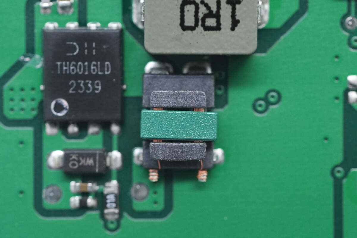
This is a transformer used to detect the output current.
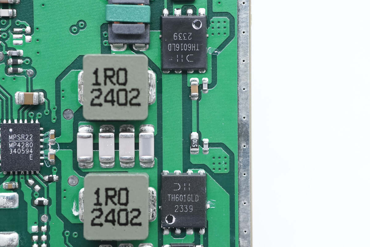
The MOSFET used to switch the wireless charging coil is from DIODES and adopts PowerDI5060-8 package. It has a withstand voltage of 60V, a resistance of 14.5mΩ, an operating temperature of 175℃, and complies with the AEC-Q101 standard. Model is DMTH6016LPDQ.

The sampling resistor is used to detect the input current of the wireless charging chip. 7mΩ.
This is an SMD inductor used for input filtering.

These are two electrolytic capacitors for input filtering.

The other wireless charging power stage chip also uses MPS MPQ4280.

Here are two alloy inductors. 1μH.
These are four NPO resonant capacitors connected in parallel.

These are three white NPO resonant capacitors.

This is a transformer used to detect the output current.

These are the two dual MOSFETs used to switch the coils.

The sampling resistor is used to detect the input current. 7mΩ.

This is an SMD inductor used for input filtering.
These are two electrolytic capacitors for input filtering.

The LIN transceiver chip marked with TL021 is from TI and adopts the SOIC8 package. It is AEC-Q100 compliant, compliant with LIN2.0, LIN2.1, LIN2.2, LIN2.2A, and ISO/DIS17987-4 standards, supports 12V applications, and supports a 4.5-36V operating voltage range. Model is TLIN1021-Q1.

The diode used to prevent power backflow is from DIODES and adopts SMA package. 1A 1000V. Model is S1M.
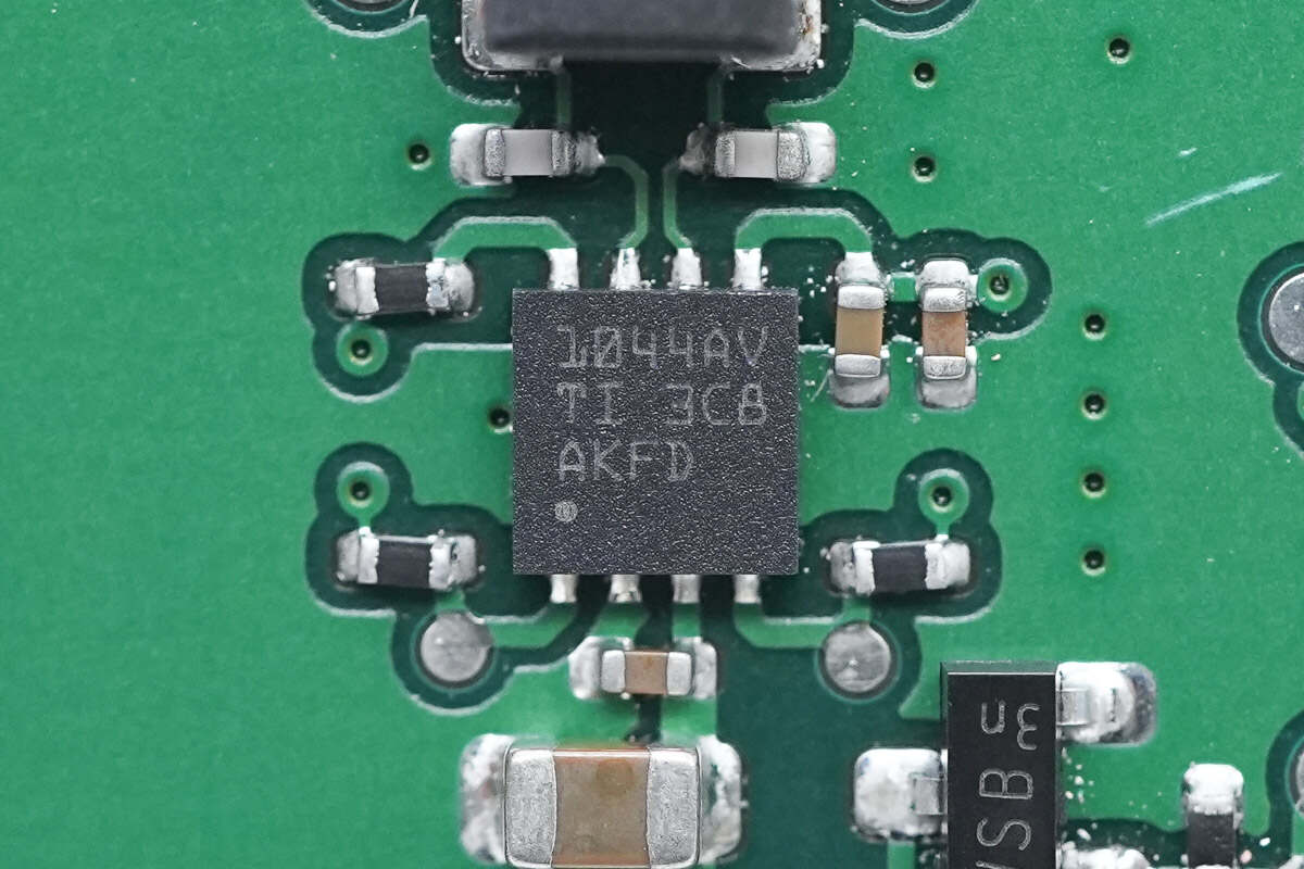
The CAN transceiver chip marked with 1044AV is from TI and adopts VSON package. It supports a 1.7-5.5V I/O voltage range, is AEC-Q100 qualified, and meets ISO 11898-2 2016 physical layer standard requirements. It supports 12 and 24V battery applications. Model is TCAN1044AV-Q1.

This is the filter inductor used in the signal path.

The wireless MCU is from TI and adopts VQFN48 package. It is a low-power Bluetooth 5.2 MCU with an integrated 48MHz ARM Cortex-M4F processor, 352kB system-programmable flash memory, 256kB ROM, 8kB SRAM, and 80kB ultra-low leakage SRAM. It supports OTA upgrades and also integrates an ultra-low power sensor controller. Model is CC2642R.

This is the external clock crystal of the chip. 48MHz.

The NFC chip is from ST and adopts VFQFPN32 package. It is an automotive-grade high-performance NFC card reader with high RF output power, low power mode, wide supply voltage range, and AEC-Q100 Grade 2 certification. It supports automatic antenna tuning and is suitable for automotive applications. Model is ST25R3914.
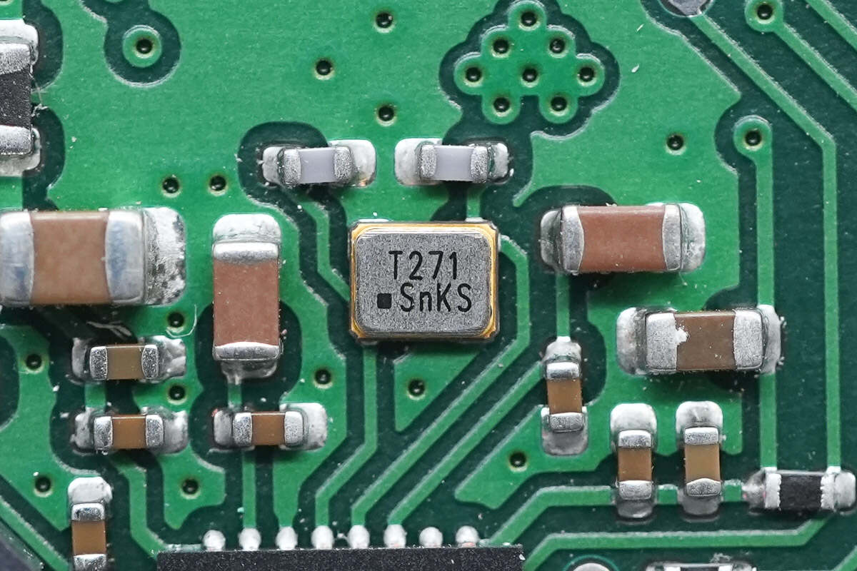
This is an external clock crystal. 27.12MHz.

The SMD inductor is used for output filtering.

This is the spring contact used to connect to the NFC coil.

Well, those are all components of the Tesla Wireless Phone Charger.
Summary of ChargerLAB

Here is the component list of the Tesla Wireless Phone Charger for your convenience.
The panel of the Tesla WC5 wireless phone charger is made of leather material, with an aluminum alloy shell inside to enhance heat dissipation, and is assembled with clips and screws. The module has two wireless charging positions, separated by a protrusion, supporting the charging of two phones at the same time.
After taking it apart, we found it uses the NXP MWCT22C3AVLH master control chip and the MPS MPQ4272 synchronous buck converter to power two MPQ4280 full-bridge power chips. The module uses automotive-grade components and is made of solid and reliable materials.
Related Articles:
1. Teardown of Tesla WC1 Wireless Phone Charger
2. Teardown of Tesla Wireless Portable Charger
3. Review of Tesla Wireless Portable Charger