Introduction
Nearly two years ago, we did a teardown video for the unique TEGIC 30W Mini Fast Charger, it got the size similar to that of a standard Apple 5W charger but can do a 30W output.
And today, we got a more powerful successor with more attractive appearance that can output 35W - the TEGIC CRYSTAL 35W GaN Charger. Besides that, have there been any significant changes in its internal components and craftsmanship? Let's find out!
Product Appearance
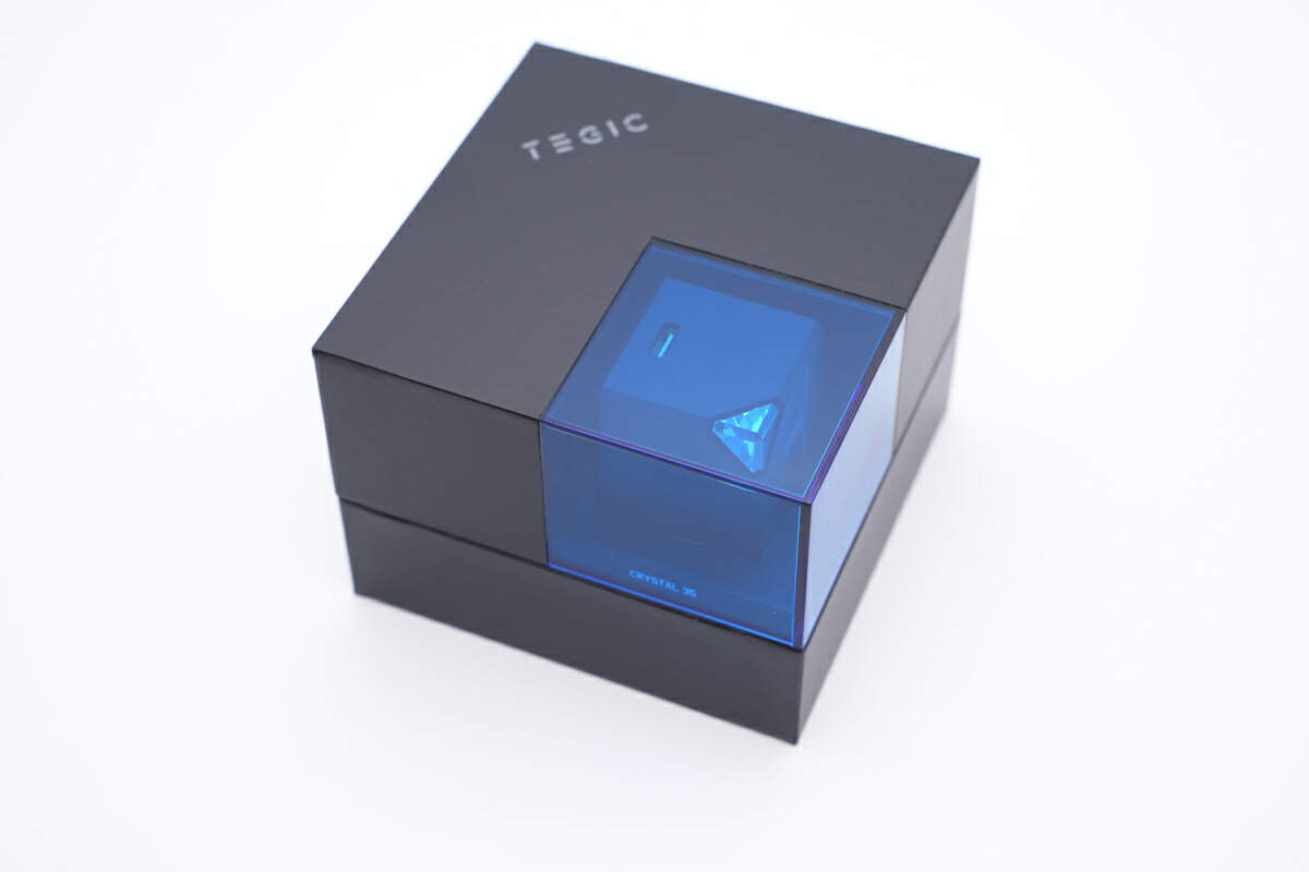
The packaging box is designed as a partially transparent cube with the charger inside, giving it a distinctive look.
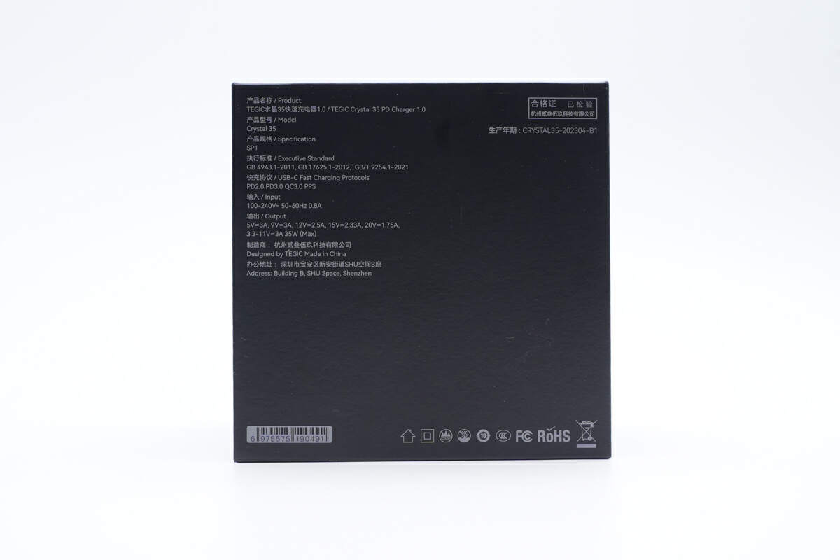
All the specs info are on the bottom, we will get to that later.
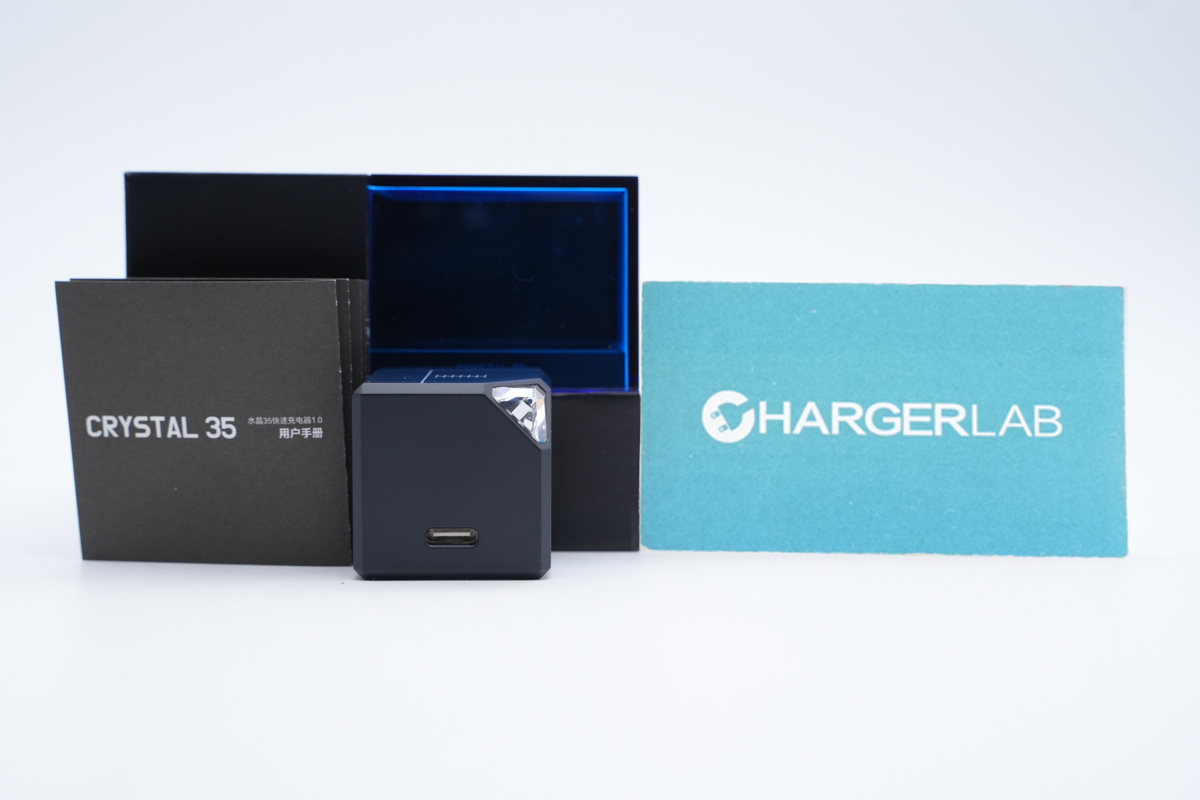
Inside the packaging, you'll find the charger and an instruction manual, but no USB cable is included.
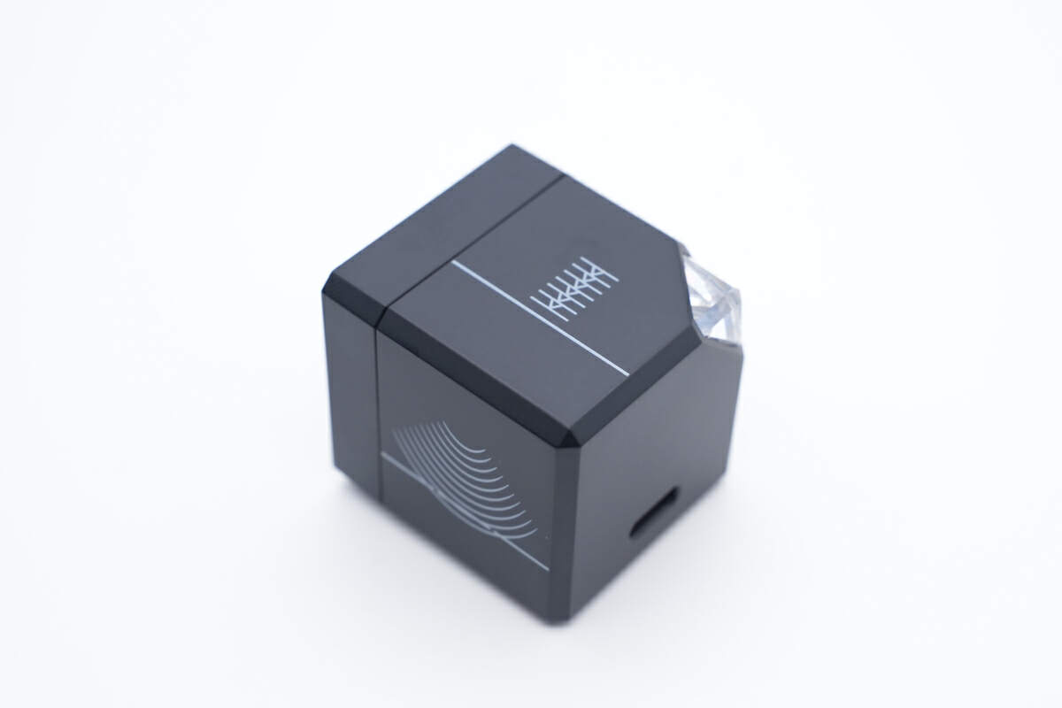
This charger is made of fire-resistant PC material, and the chamfered edges make it feel smooth.
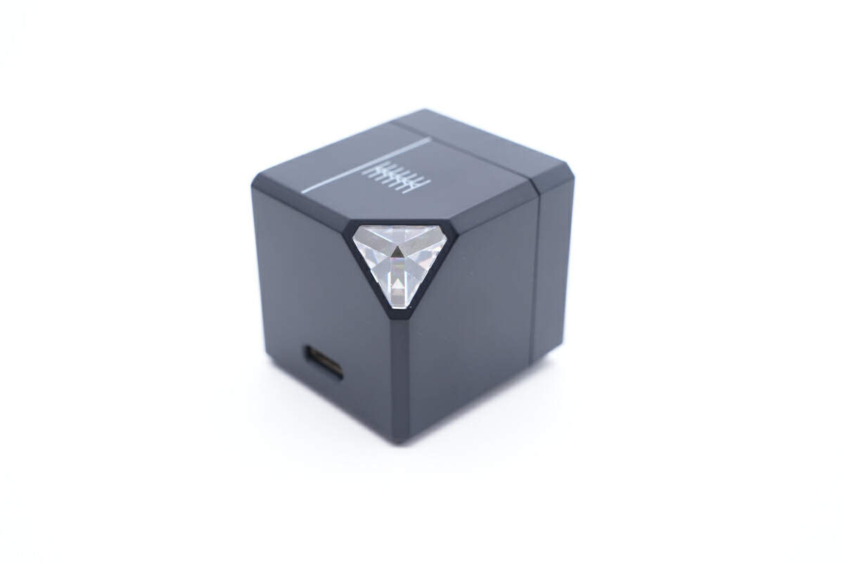
The diamond-shaped LED light in the corner makes you think that the internal structure is a giant crystal block. It can also function as a night light, pretty cool.
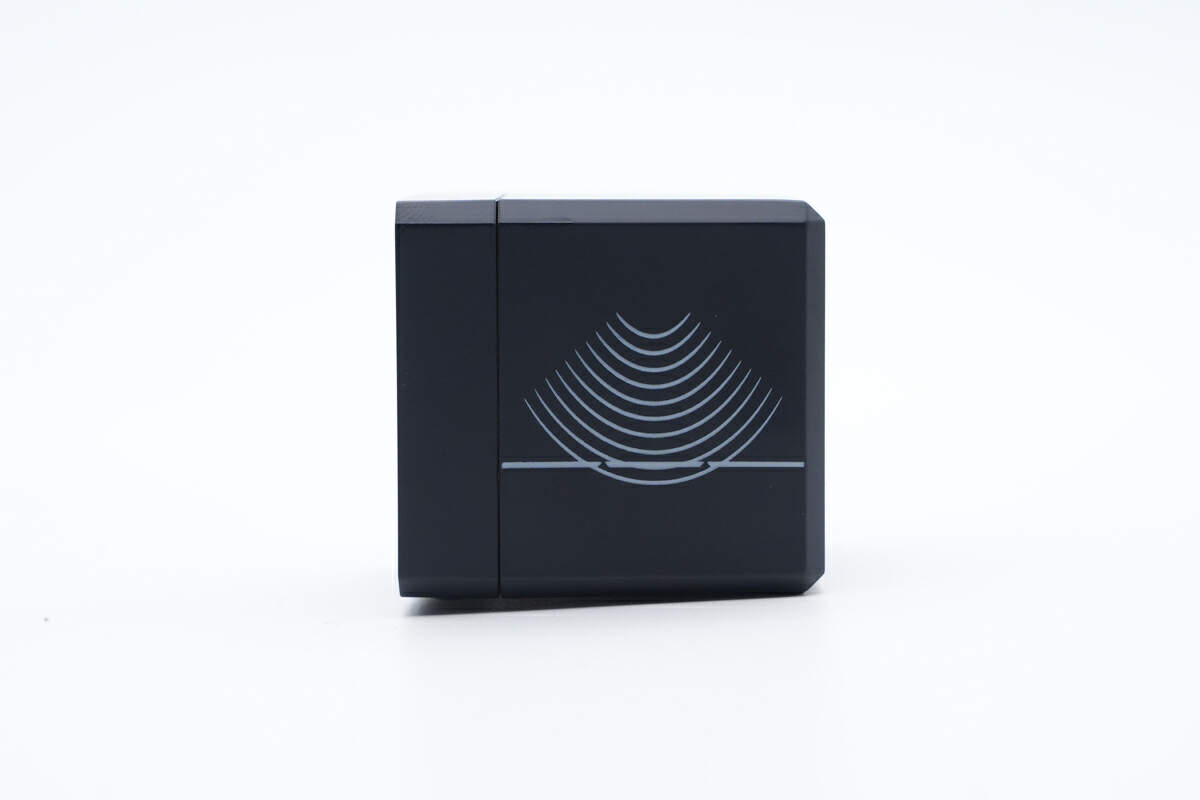
The side of the charger features a well-known physics experiment diagram called "double-slit interference."
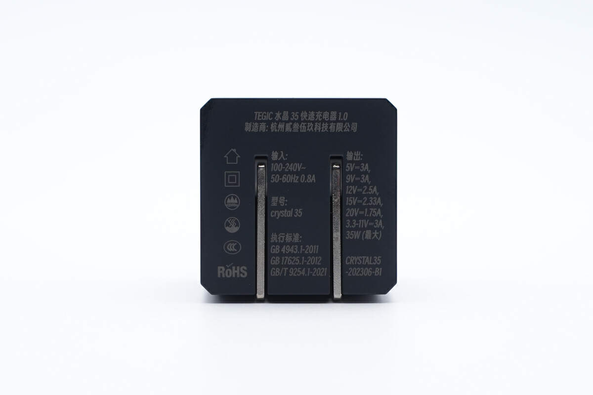
The model is equal to its official name, which is crystal 35. It can support input of 100-240V~50/60Hz 0.8A. The maximum output is 20V1.75A, which is 35W.
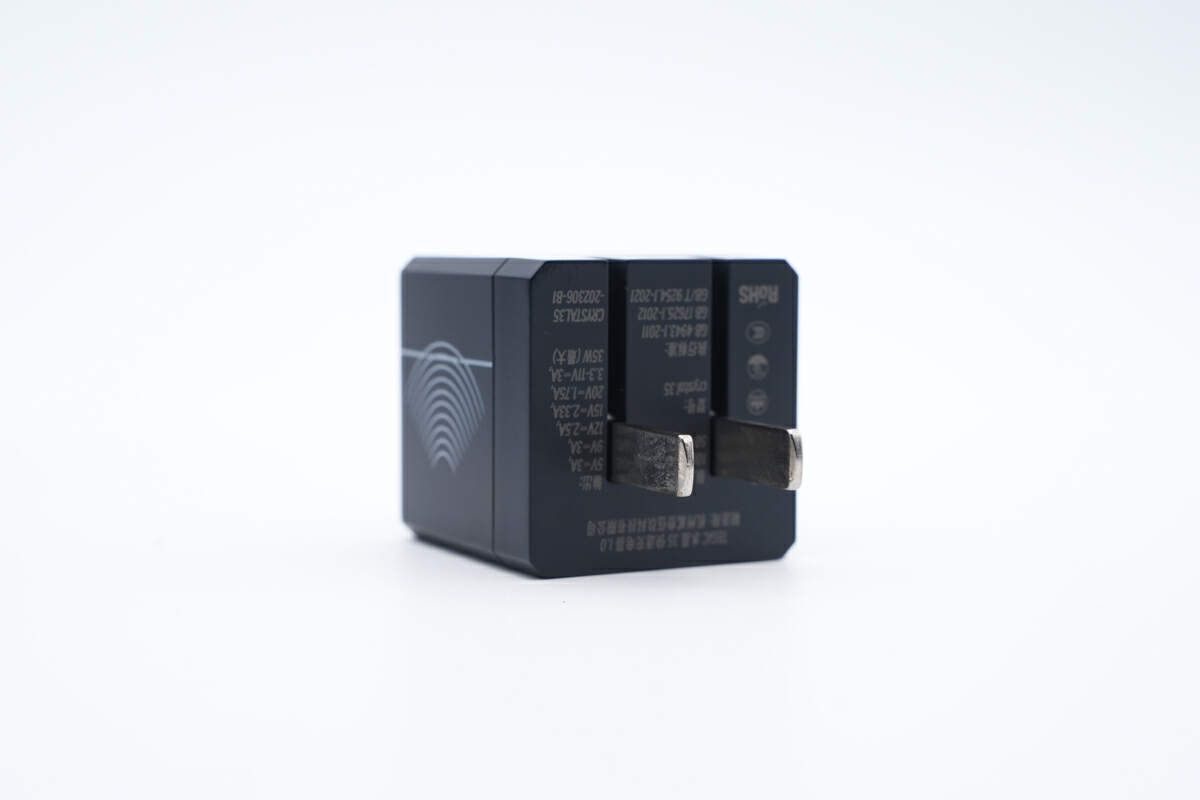
Compared to the previous generation, the input prongs become foldable.
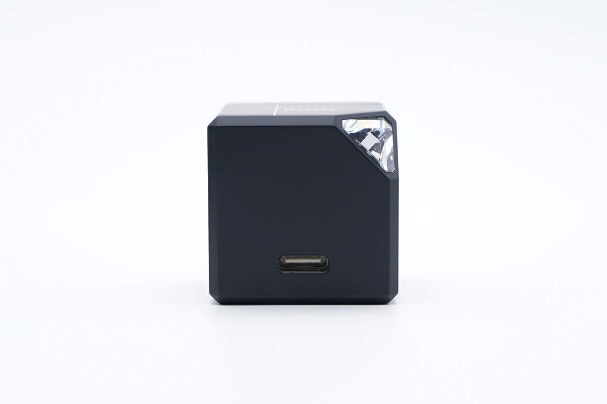
The USB-C port is not positioned in the center.
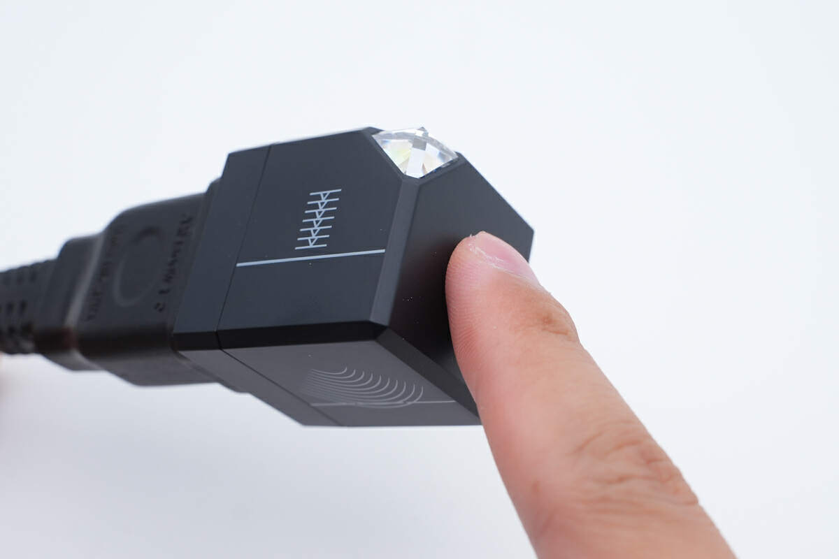
In the center area, there is a hidden touch switch used to control the LED light.
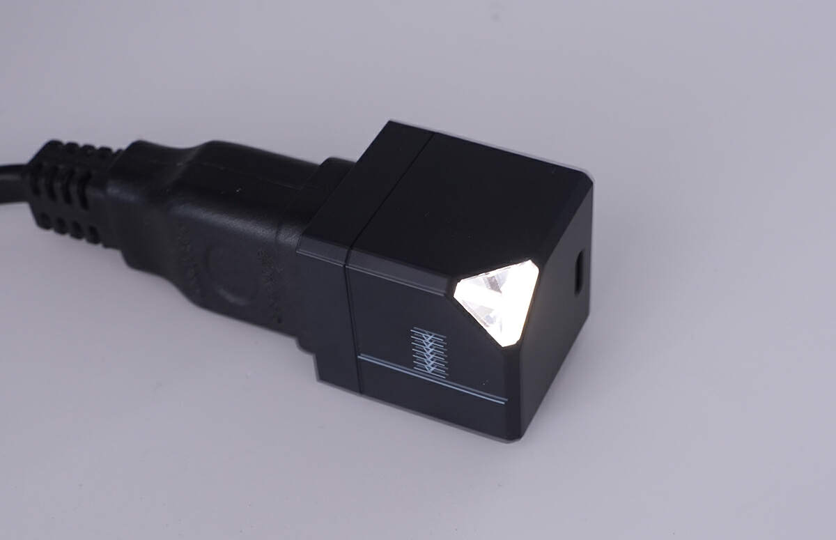
And it will light up in a beautiful way.
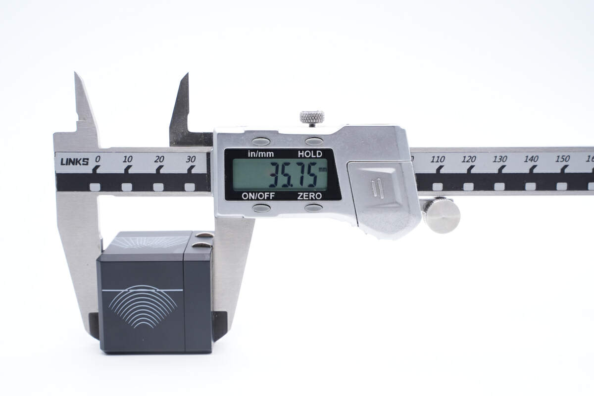
The length of the charger is about 36mm (1.42 inches).
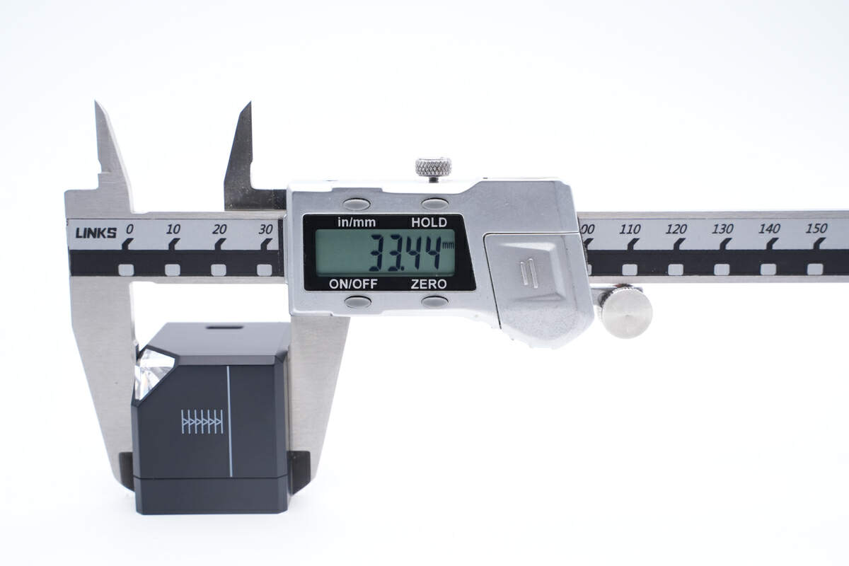
The width is about 33.5mm (1.32 inches).
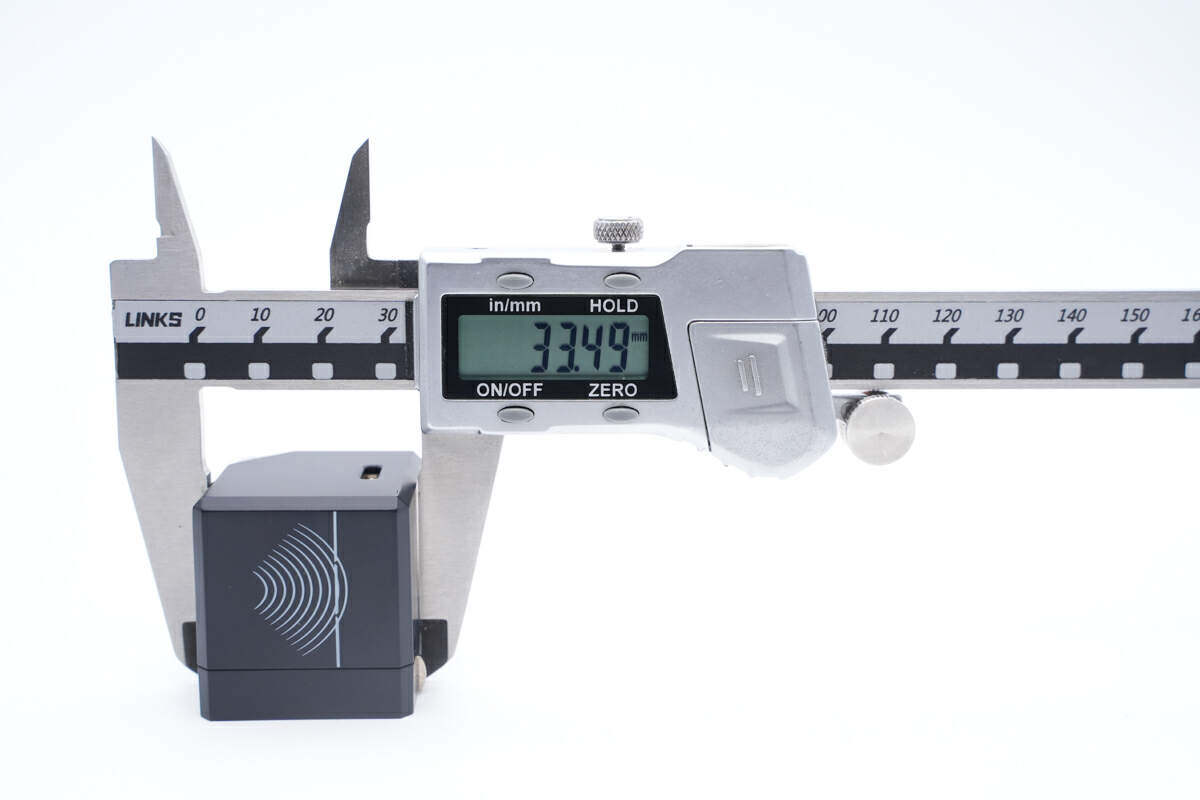
And the height is also about 33.5mm (1.32 inches).
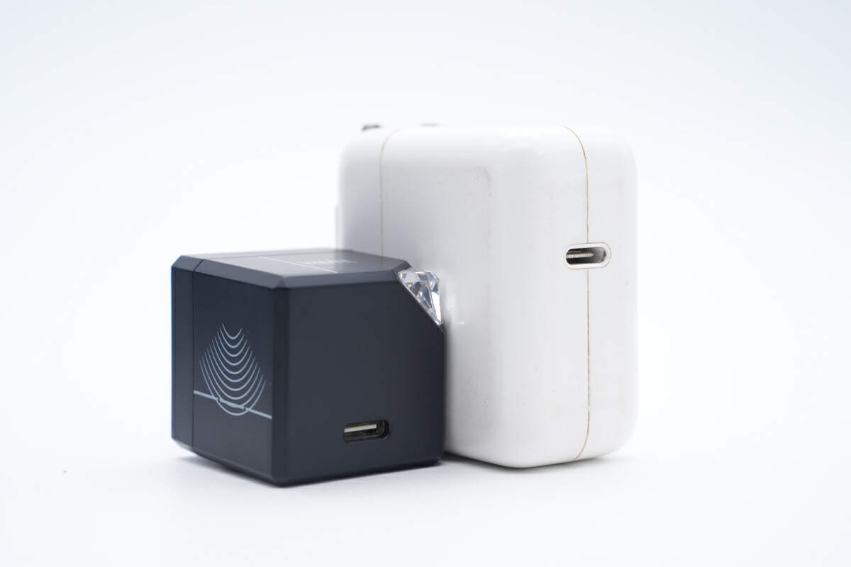
As you can see, it's noticeably smaller than the Apple 30W charger.
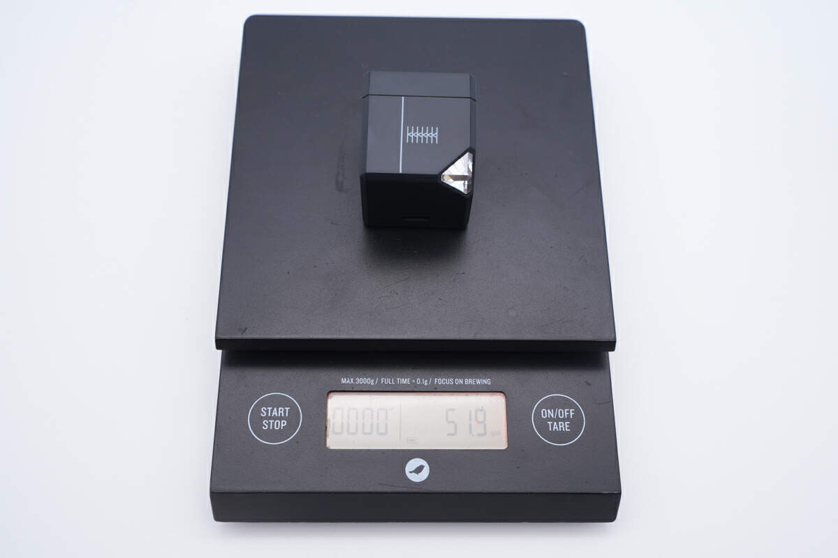
And the weight of this charger is about 52g (1.83 oz).
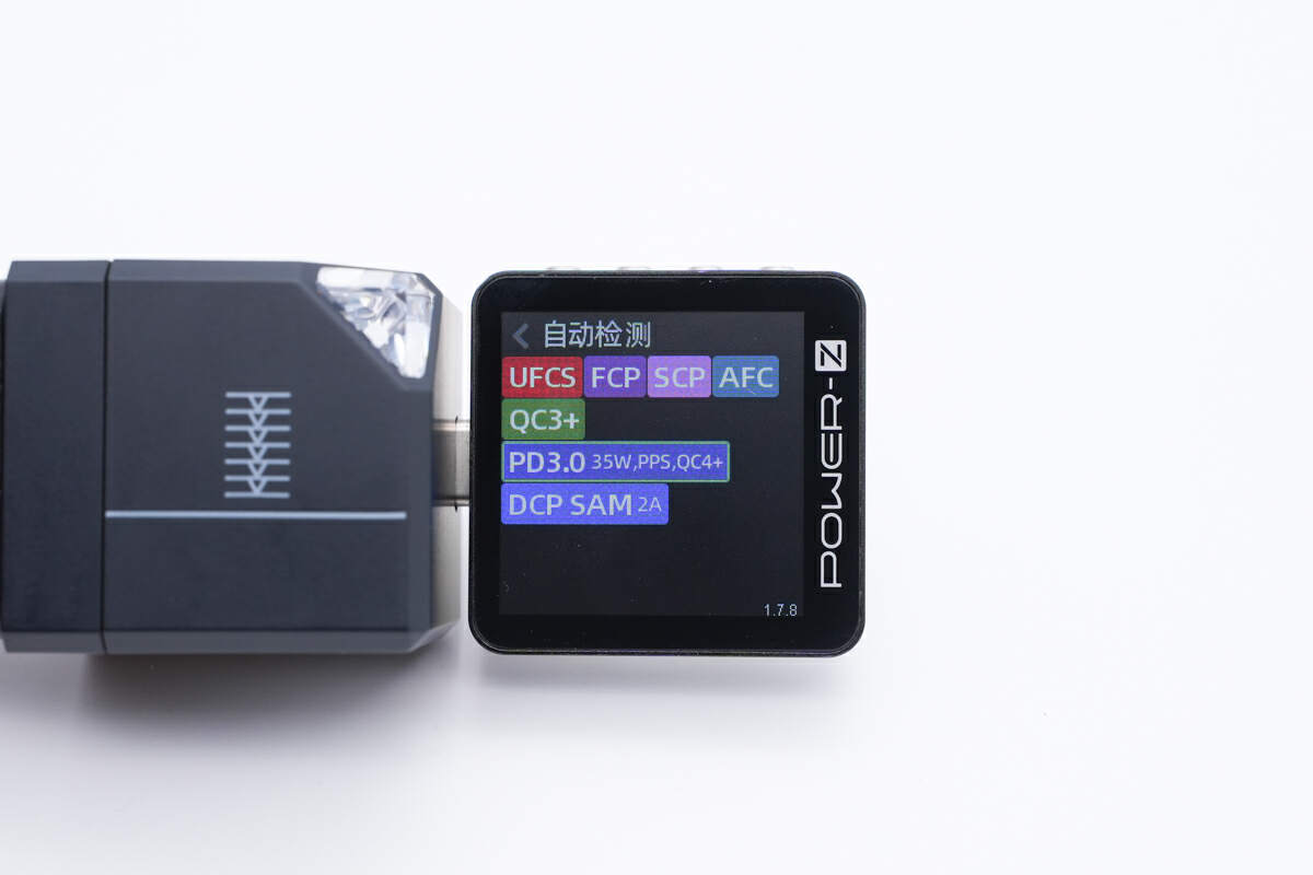
ChargerLAB POWER-Z KM003C shows it can support UFCS, FCP, SCP, AFC, QC3+/4+, PD3.0, PPS, DCP and SAM 2A charging protocols.
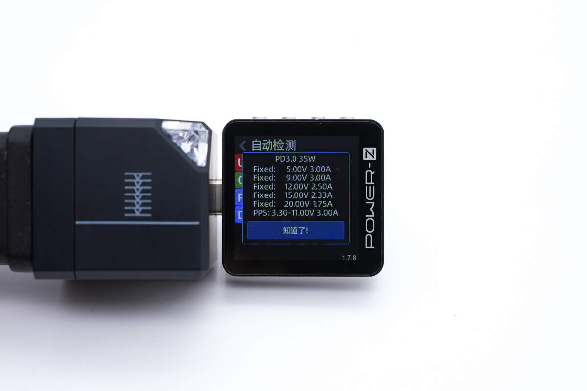
And it has five fixed PDOs of 5V3A, 9V3A, 12V2.5A, 15V2.33, 20V1.75A and a set of PPS, which is 3.3-11V3A.
Teardown
Now comes the exciting part - the teardown.
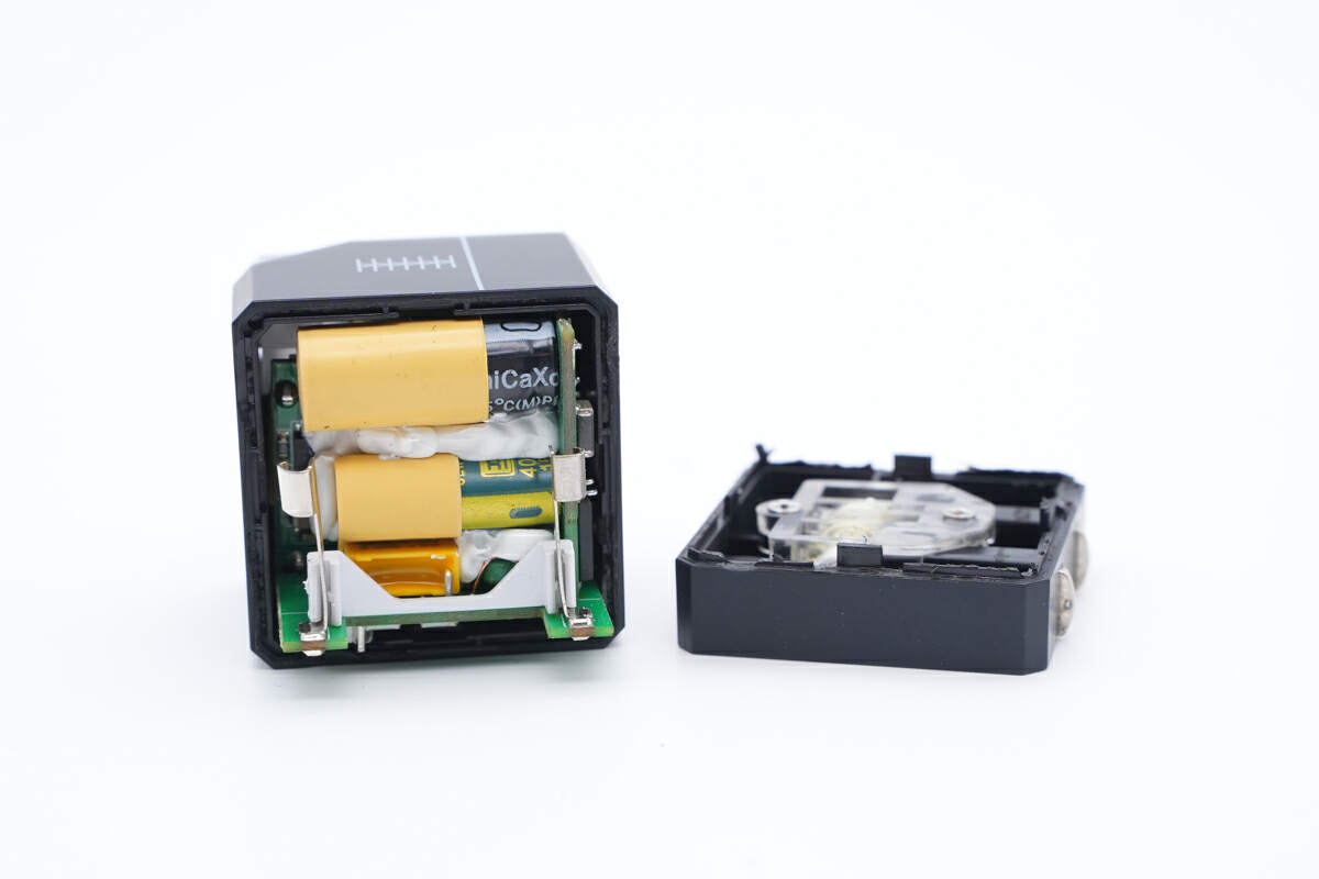
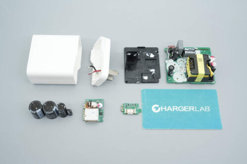
As usual, use a spudger to pry along the gap and open the bottom cover. The input prongs are directly connected to the PCBA module without wires.
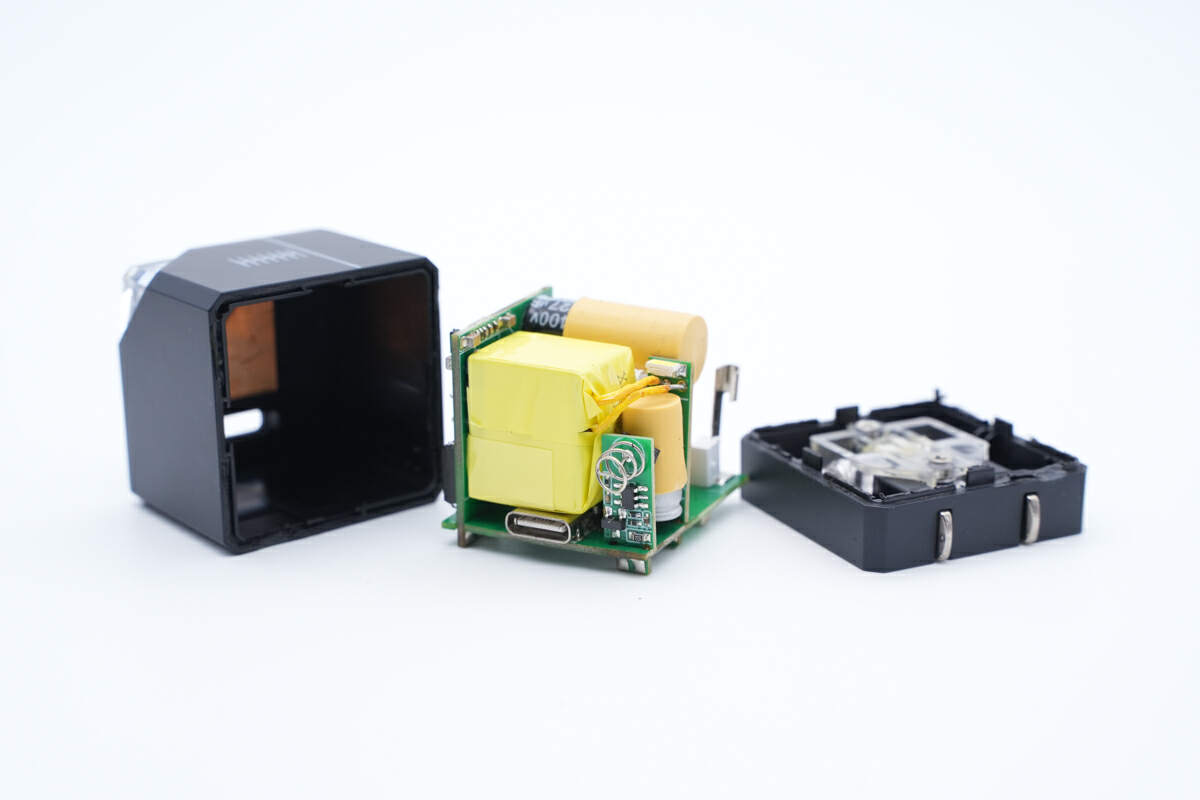
The PCBA module is composed of multiple small PCBs to make full use of space.
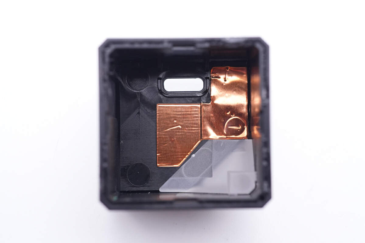
The copper foils inside the charger are used to detect touches.
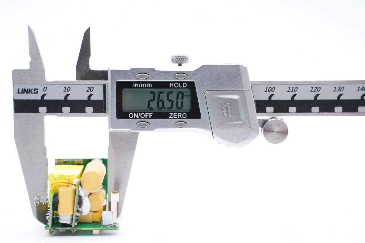
The length of the PCBA is 26.5mm (1.04 inches).
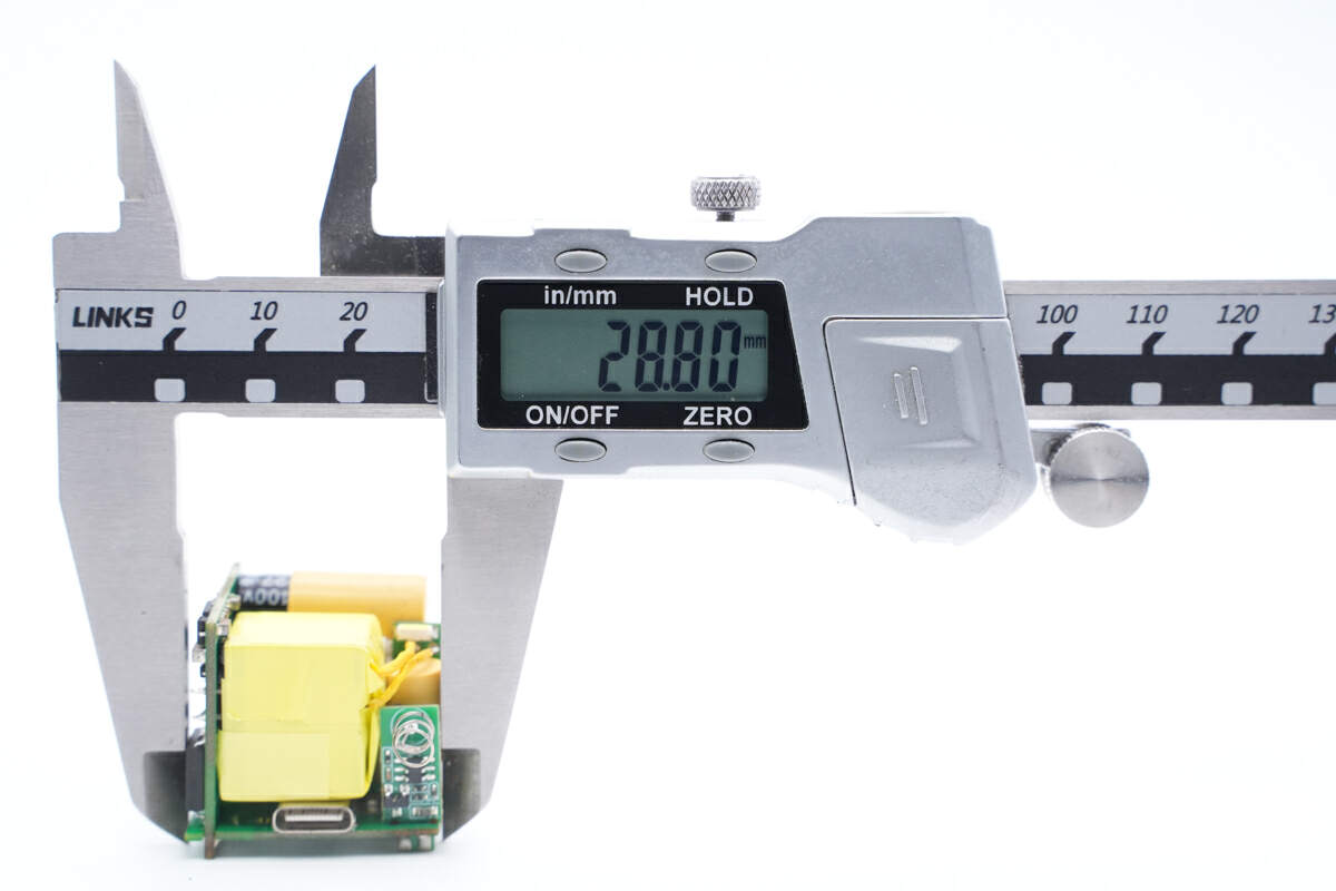
The width is also about 29mm (1.14 inches).
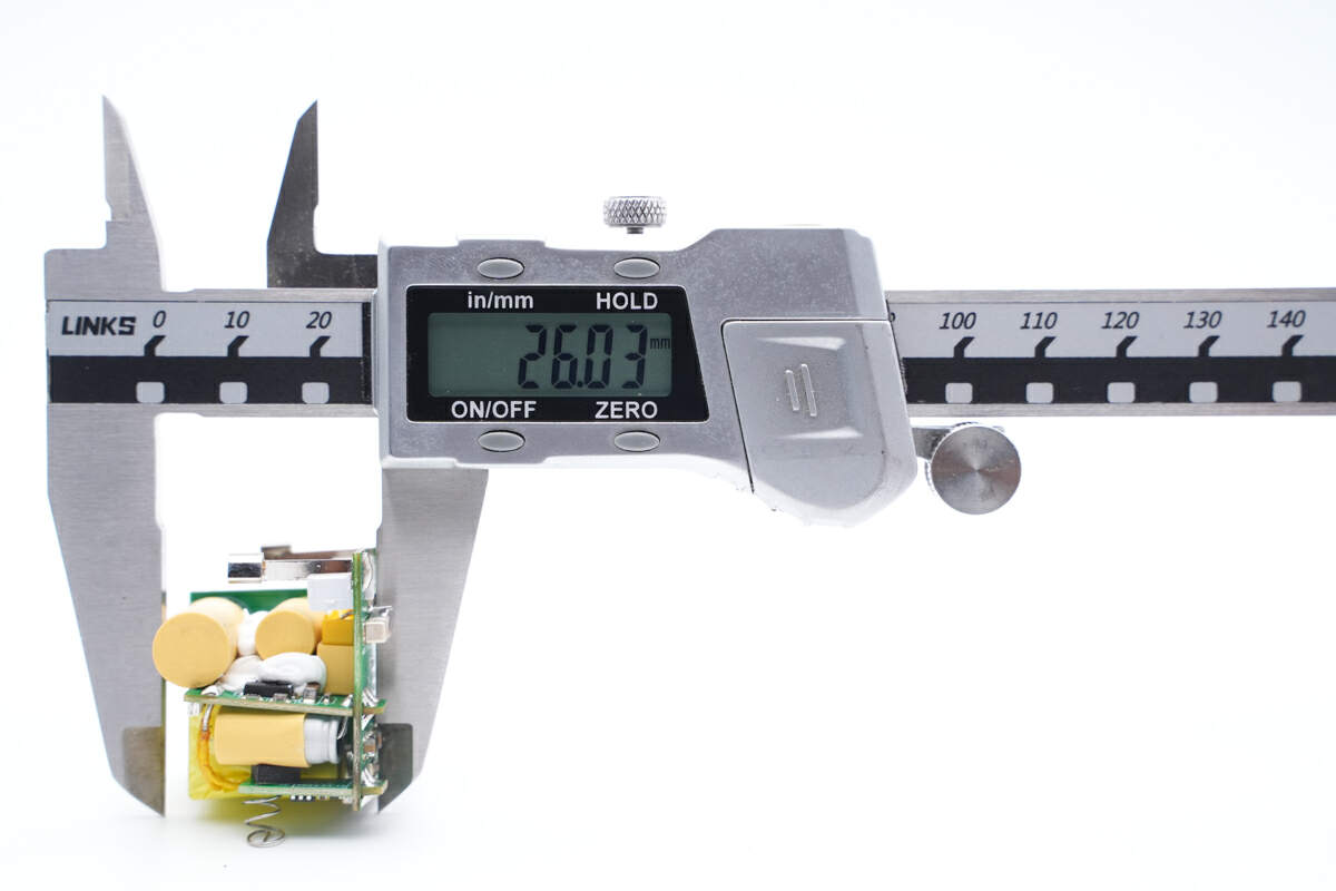
And the height is about 26mm (1.02 inches).
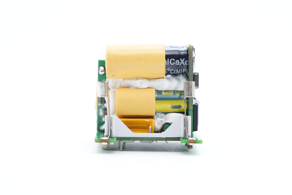
There is a significant amount of potting compound used to secure various components. The high-voltage electrolytic capacitors have yellow sleeves, which closely resemble the internal design of the previous generation.
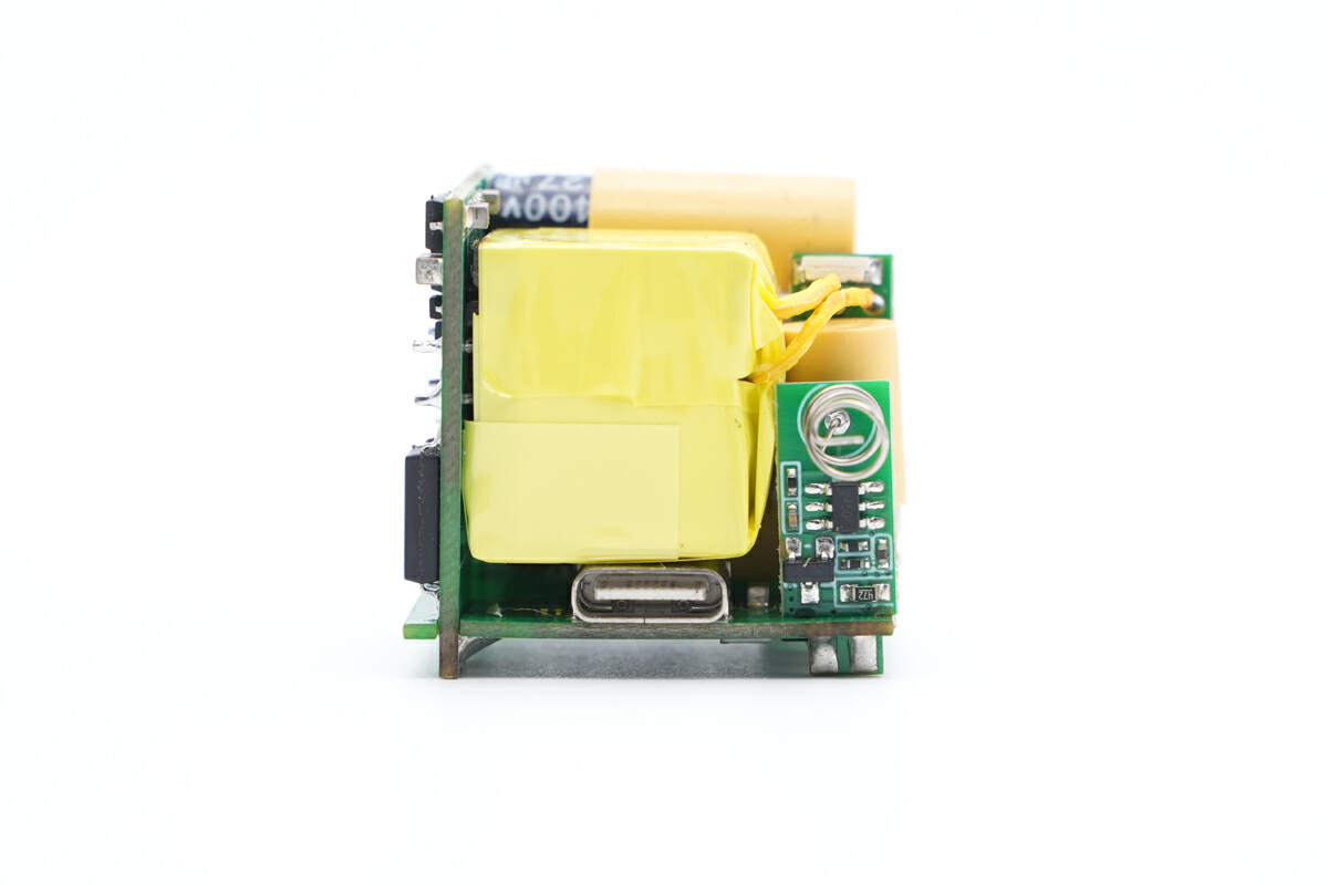
A large transformer occupies a substantial space in the middle, explaining why the USB-C port is not in the center.
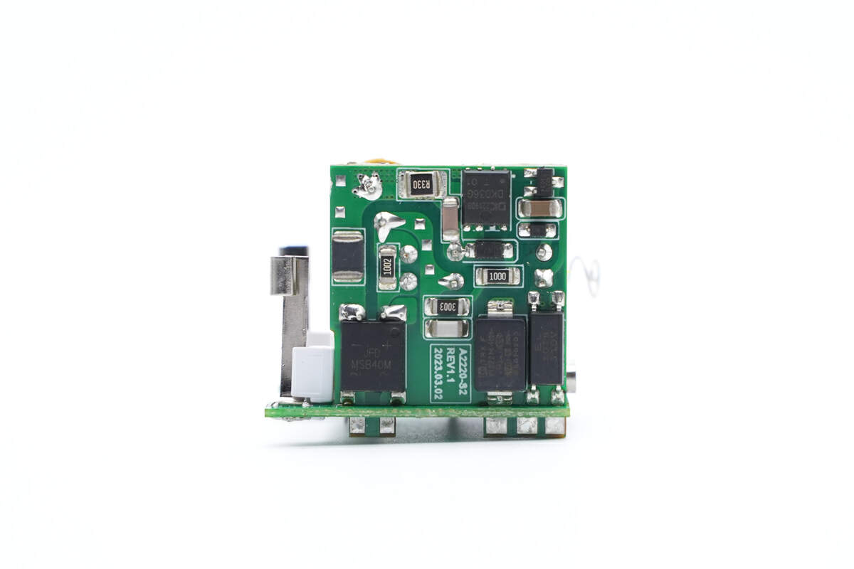
The first PCB features several components, including a bridge rectifier, GaN IC, Y capacitor, and optocoupler.
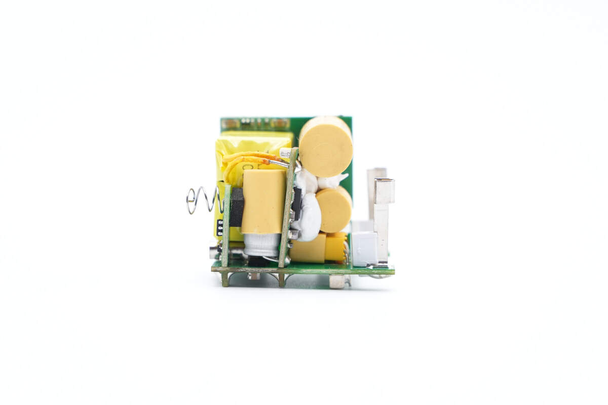
The second PCB is fixed with two small PCBs, one for LED light control and the other for synchronous rectification. The solid capacitor between them for output filtering also have rubber sleeves.
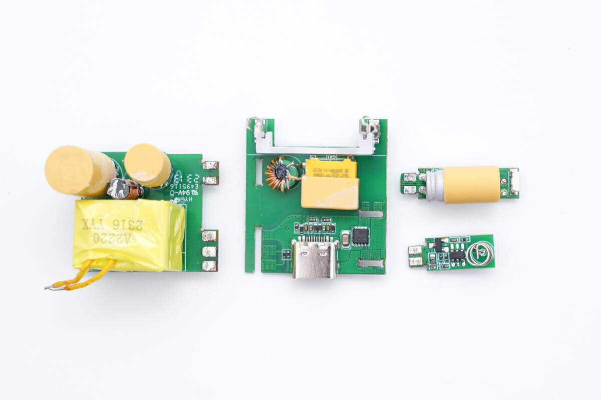
We split the four PCBs for a better observation. ChargerLAB found that it uses a QR flyback topology composed of GaN IC and a synchronous rectifier chip, with the output voltage being regulated by the protocol chip through an optocoupler. Now, let's start by examining the information of various components, starting from the second PCB.
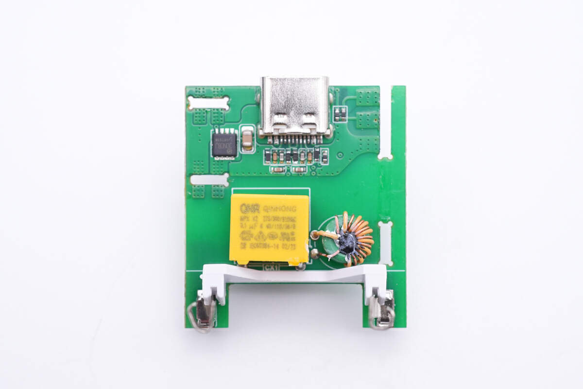
The X2 safety capacitor, common mode choke, VBUS MOSFET and USB-C female socket are on the front.
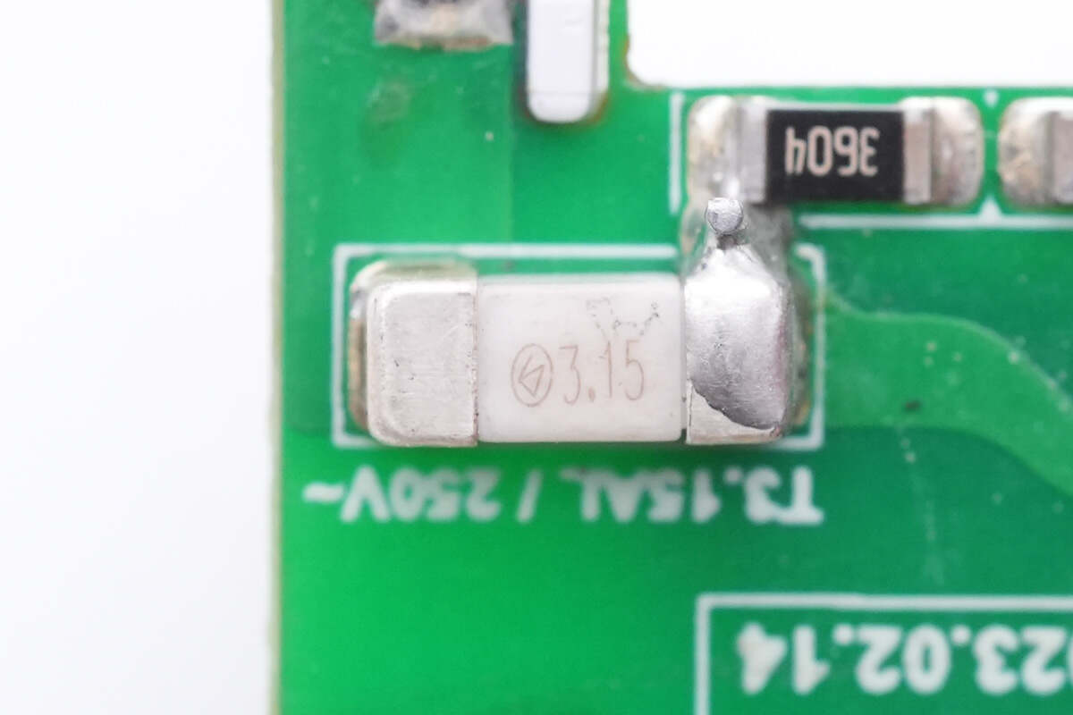
The input fuse is from Betterfuse 244 series. 3.15A 250V.
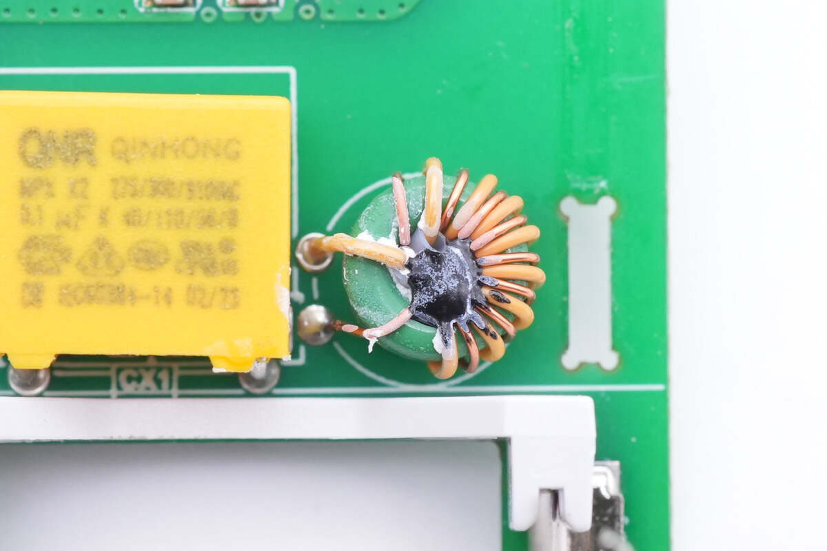
The common mode choke is wound with magnet wires and insulated wires.
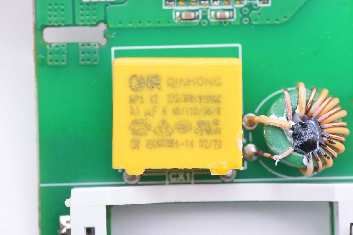
The safety X2 capacitor next to it is from QNR. 0.1μF.
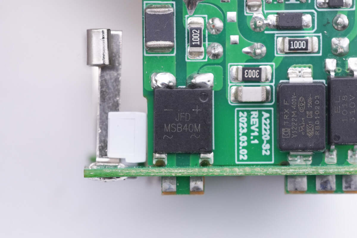
This bridge rectifier is on the first PCB, model is MSB40M. 4A 1000V.
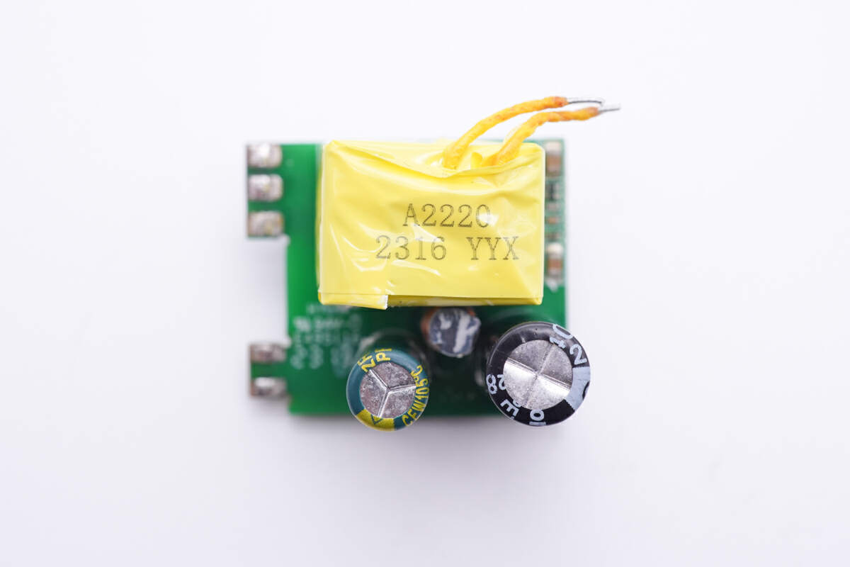
Flip to the front, it has a big transformer, filter capacitor and common mode choke.
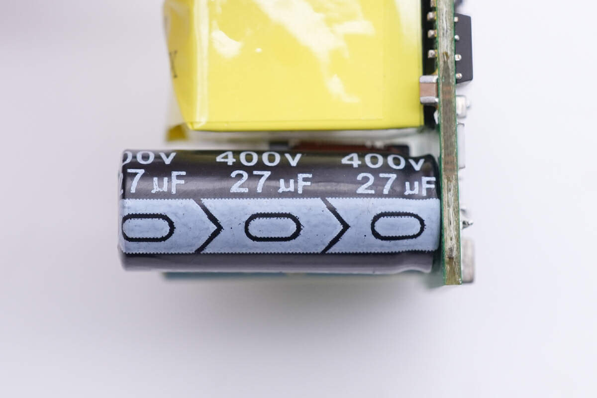
This electrolytic capacitor for input filtering is next to the transformer. 400V 27μF.
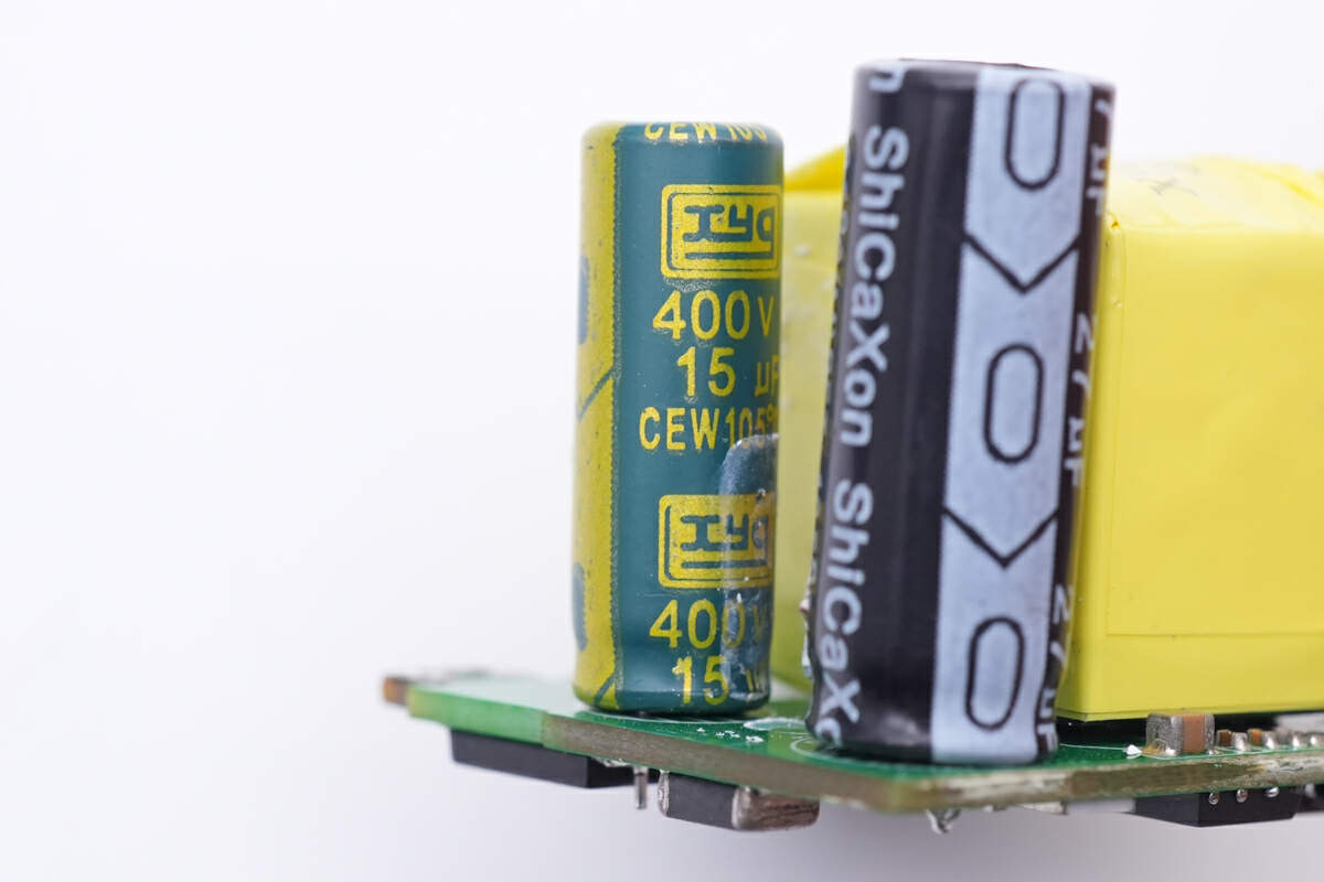
And this smaller one is 400V 15μF.
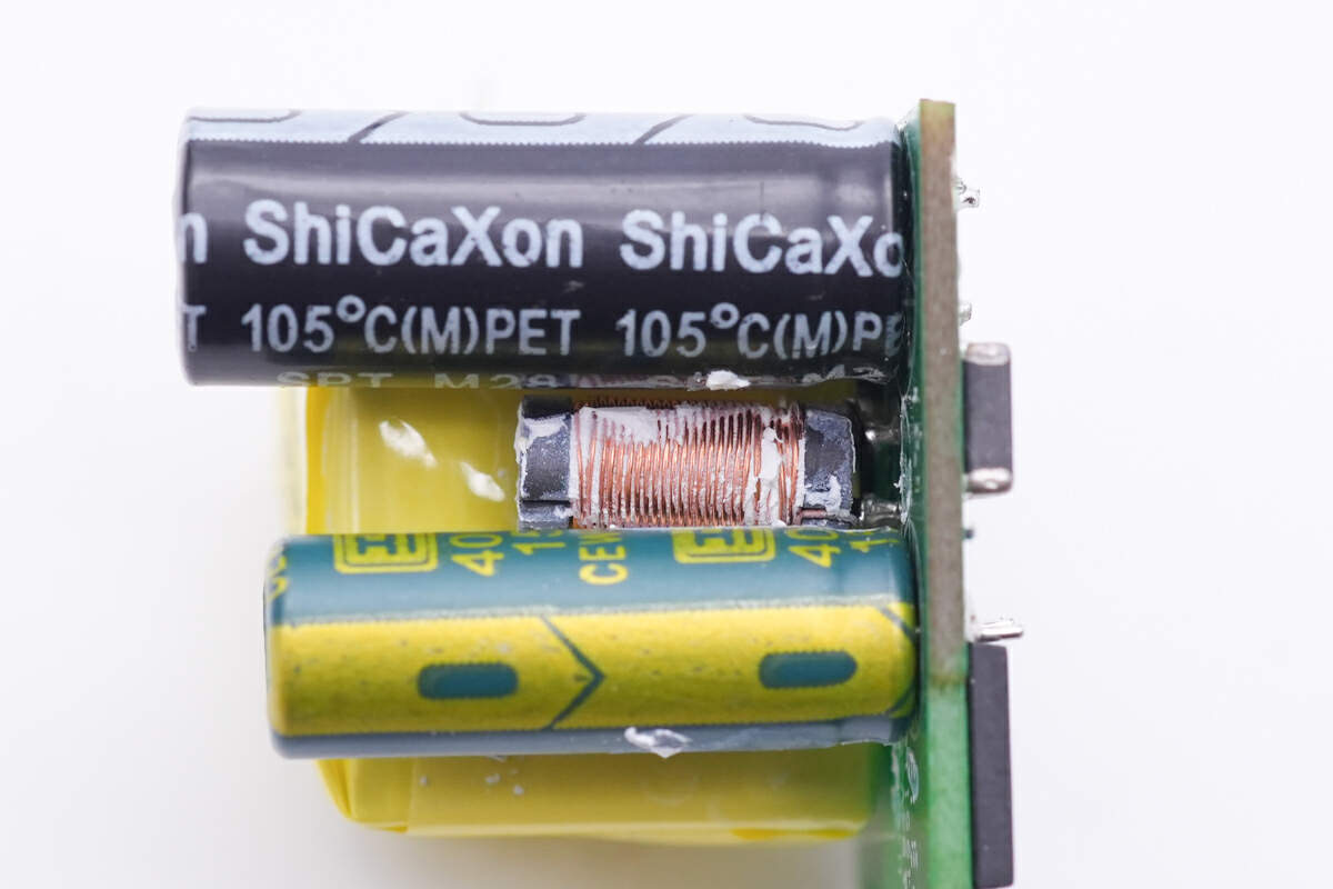
A differential mode choke is between them.
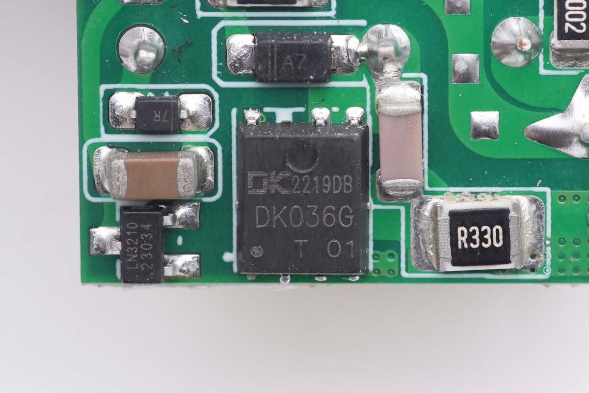
The master control chip is from Dongke, model DK036G, which is a QR flyback control AC-DC chip integrated with a 650V/400mΩ GaN FET. It can detect the voltage between the drain and source of the MOSFET, aka VDS. When VDS reaches its lowest value, it turns on the MOSFET, reducing losses and improving electromagnetic interference (EMI).
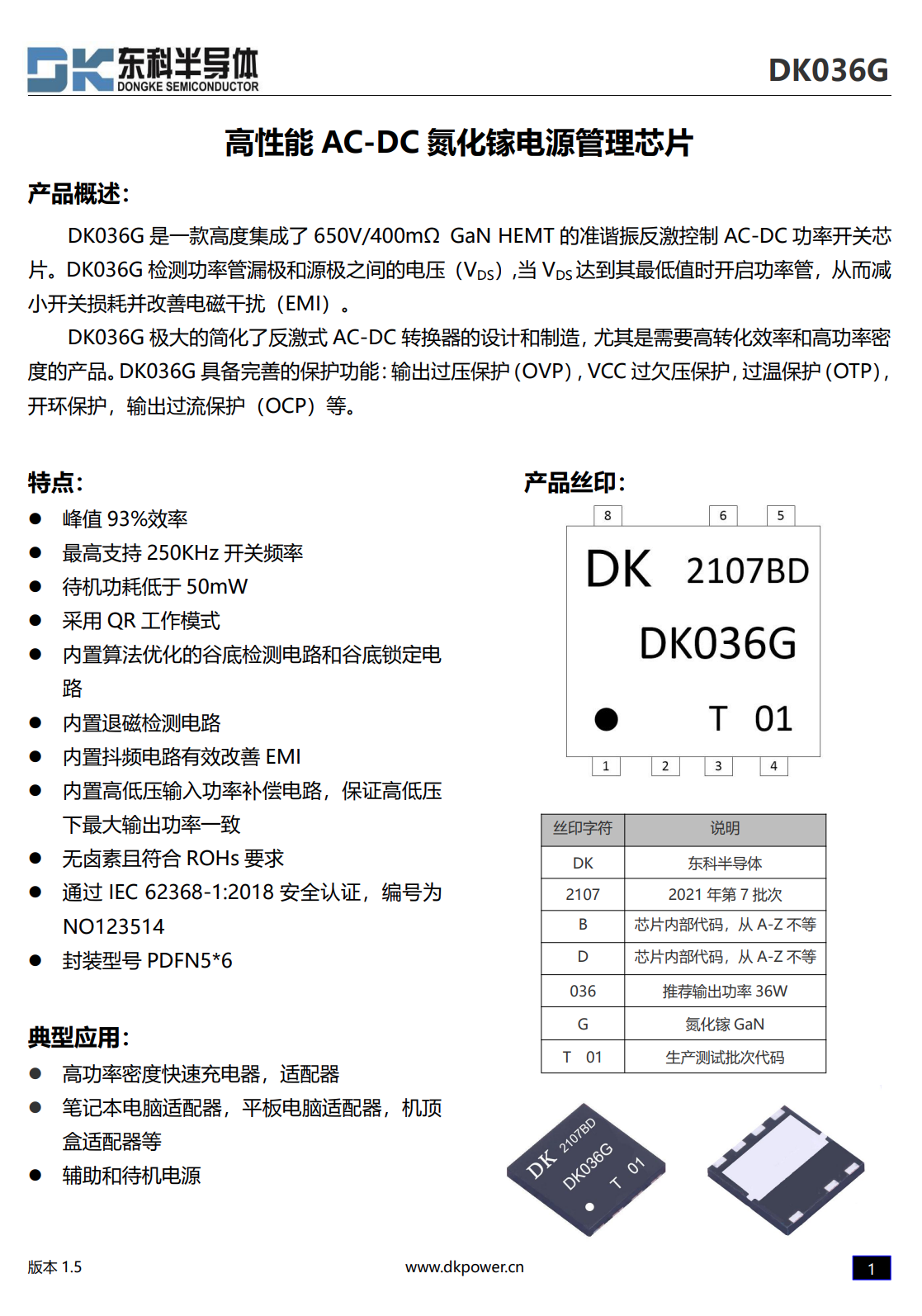
Additionally, it incorporates a high and low voltage input power compensation circuit, suitable for various applications such as GaN chargers. It comes in a PDFN5x6 package.
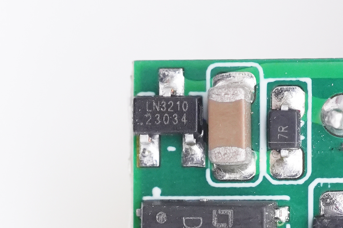
This high-performance power management IC that powers the master control chip is from Lii Semi, with the model LN3210. It's capable of handling input voltages up to 75V with low standby power consumption.
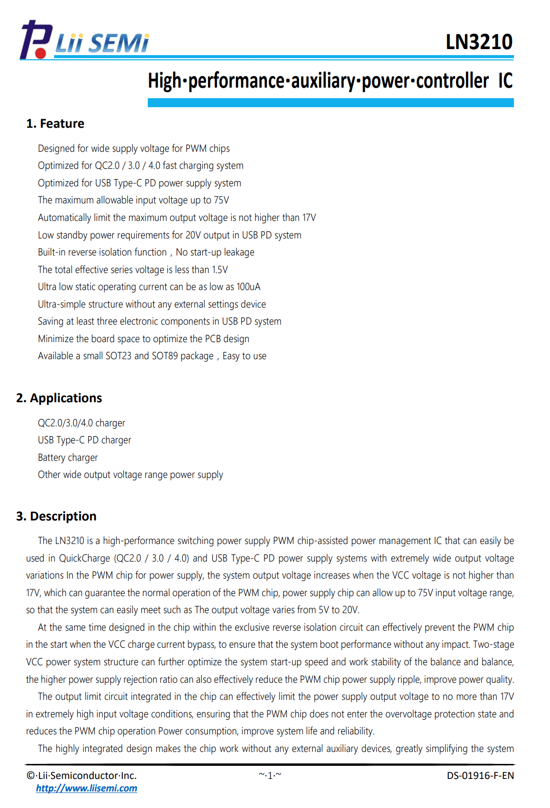
It only has 3 pins, making it user-friendly and suitable for fast charging power supplies and other applications. It is available in two packages: SOT23 and SOT89.
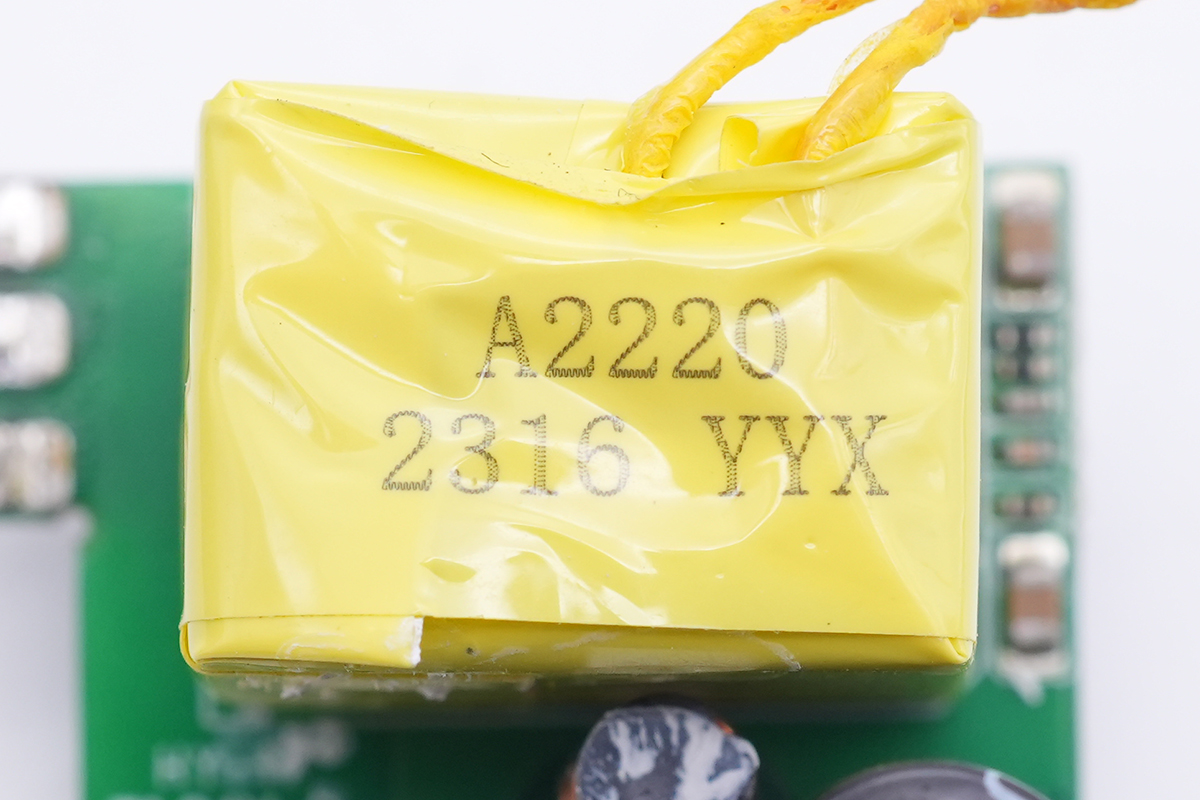
The transformer is insulated with yellow tape.
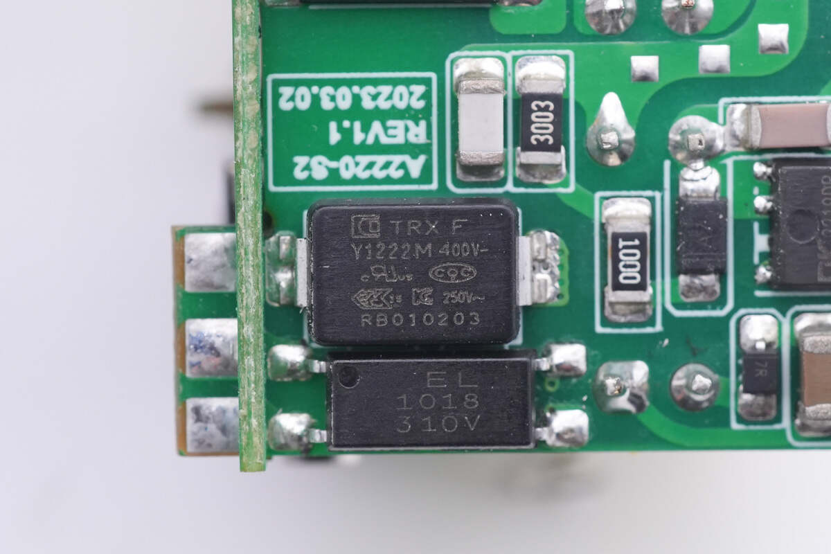
The SMD Y capacitor is from TRX, model TMY1222M, which features in small size and light weight.
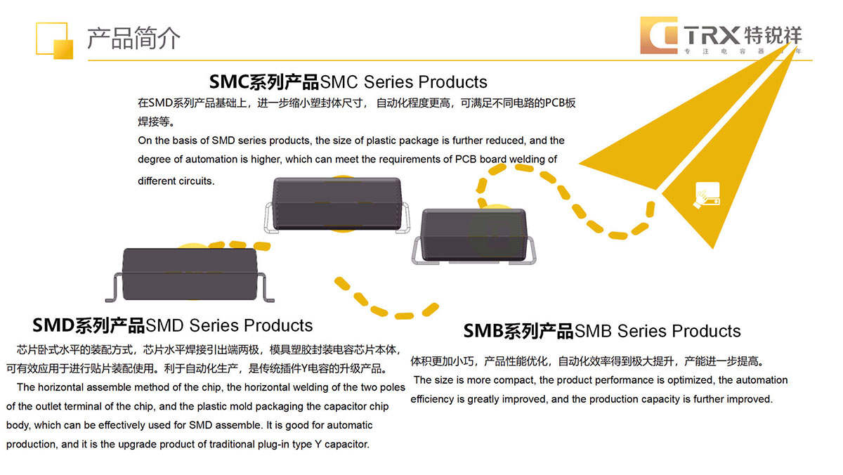
And it is very suitable for high-density power supply products such as GaN charger.
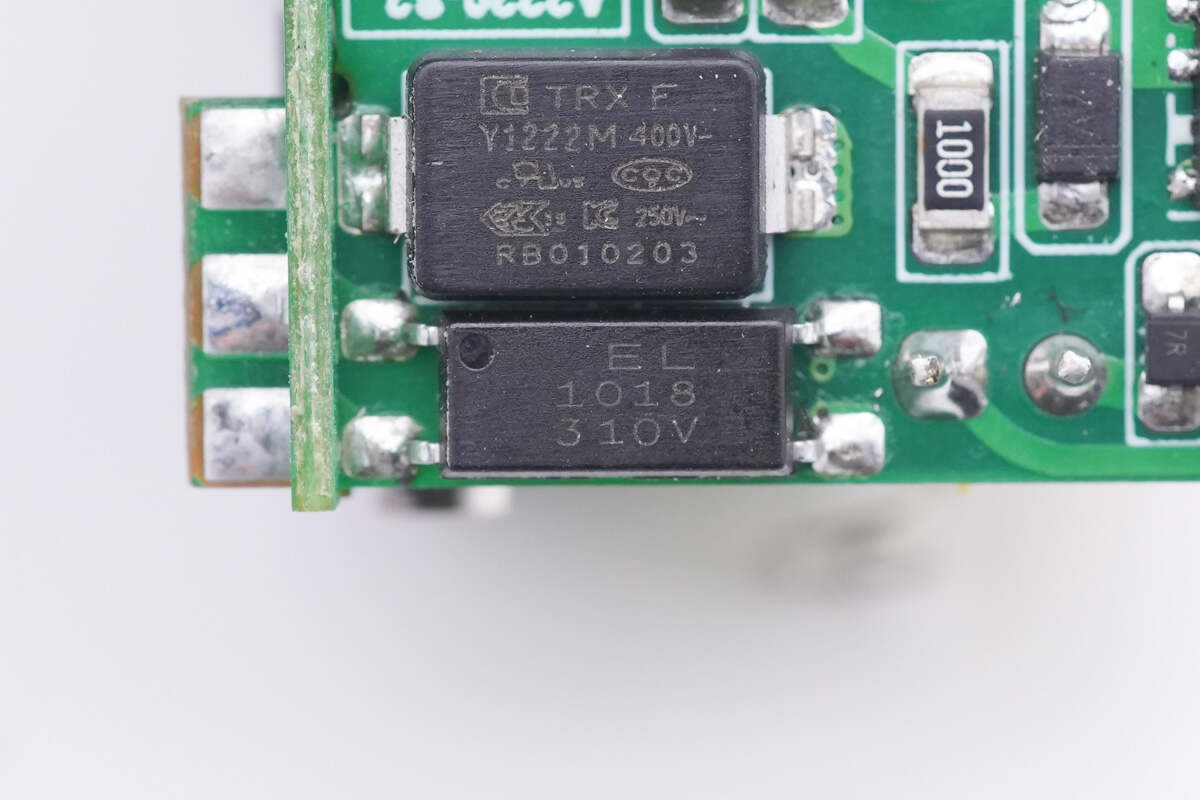
This EL1018 optocoupler right next to it is from EVERLIGHT, and it's used for providing feedback on the output voltage.
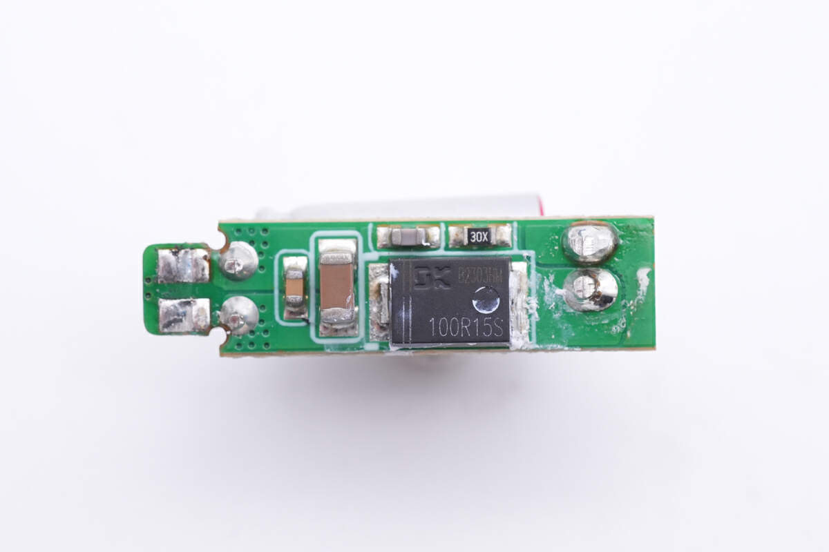
Moving on to one of the small PCBs.
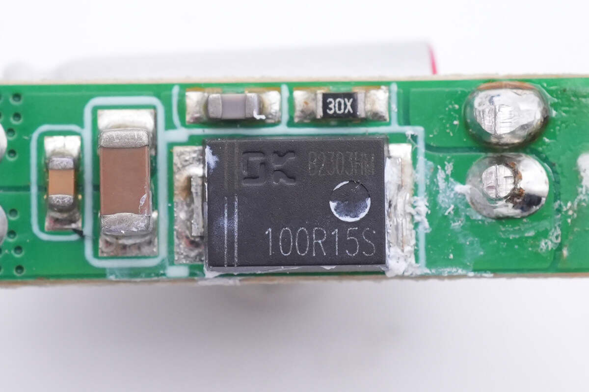
This synchronous rectification chip marked with 100R15S is from Dongke, with the model DK5V100R15S. It doesn't require external components and comes with an integrated 100V/15mΩ MOSFET. It also features self-powering technology, and it can replace Schottky diode directly.
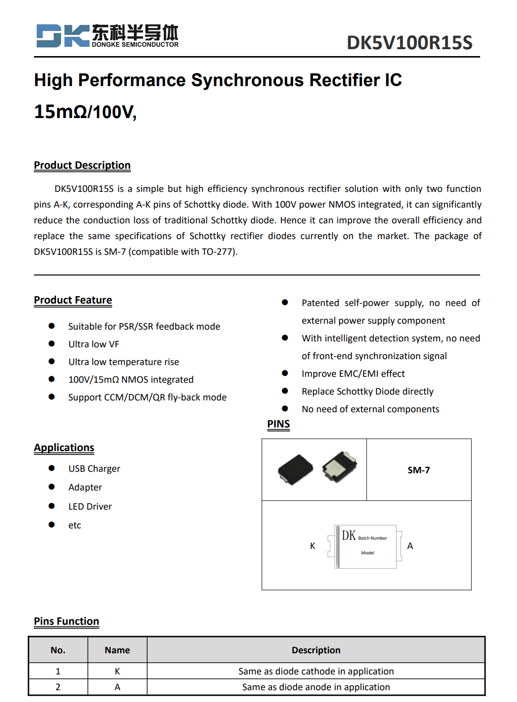
This chip supports various working modes, including CCM, DCM, and QR. It is suitable for applications such as PD chargers and LED drivers. It comes in an SM-7 package.
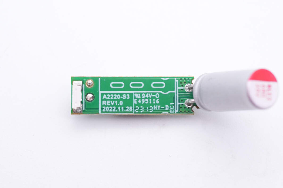
Flip to the back, there is a solid capacitor on one end.
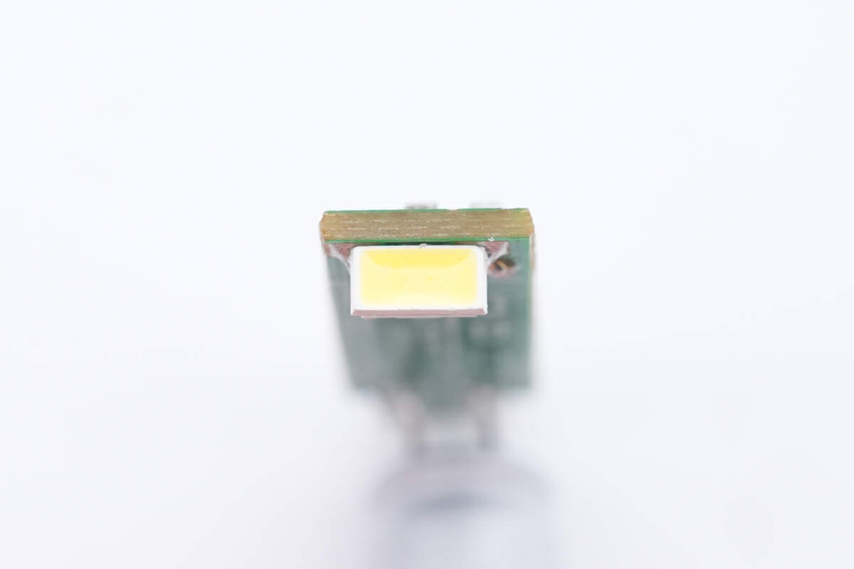
And an LED light on the other end.
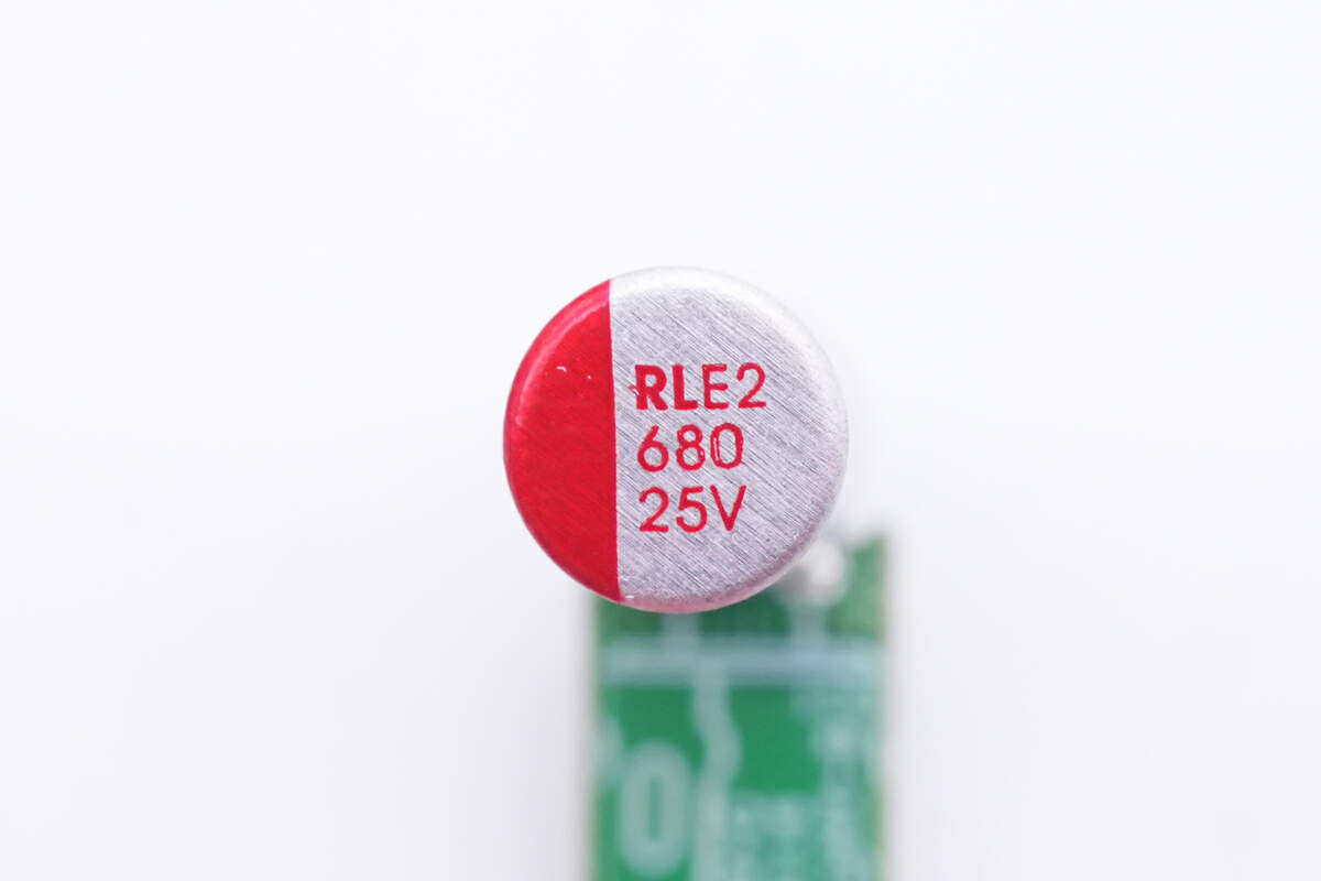
The solid capacitor for output filtering is from Reloncap. 680μF 25V.
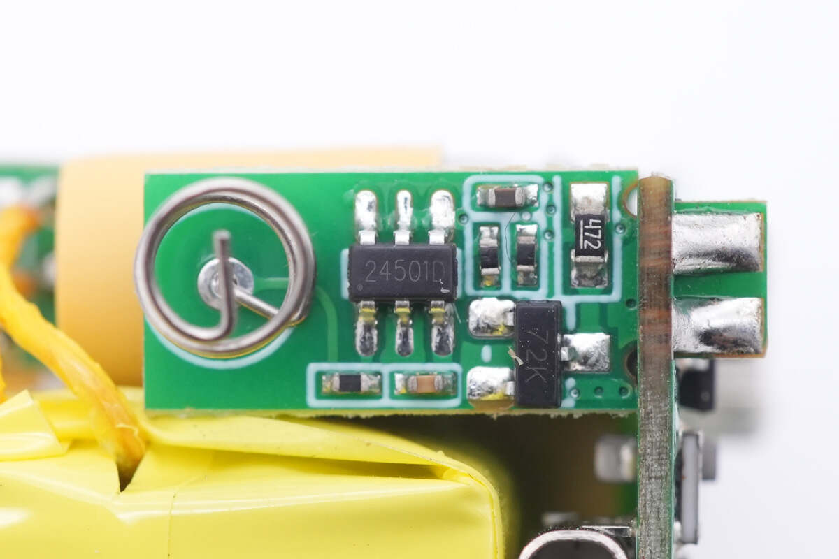
The chip next to the spring is marked with 24501D, which is used to detect touch and control the LED light. And the spring is physically connect to the copper foils inside the charger we talked about before.
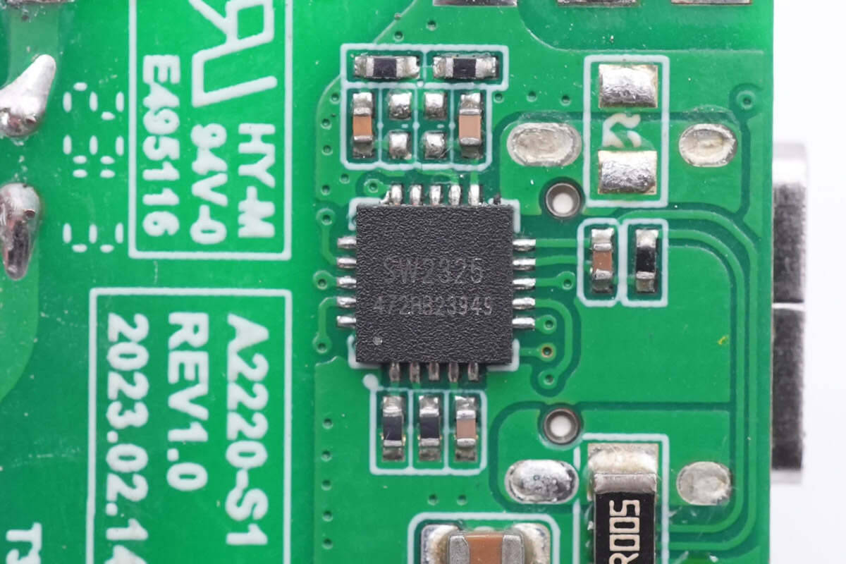
The protocol chip is from iSmartWare, model SW2325, which is used to control the USB-C/USB-A port. It has an embedded ARM Cortex-M0 core, 64KB eFlash, 4KB SRAM, and supports I2C and UART interface.
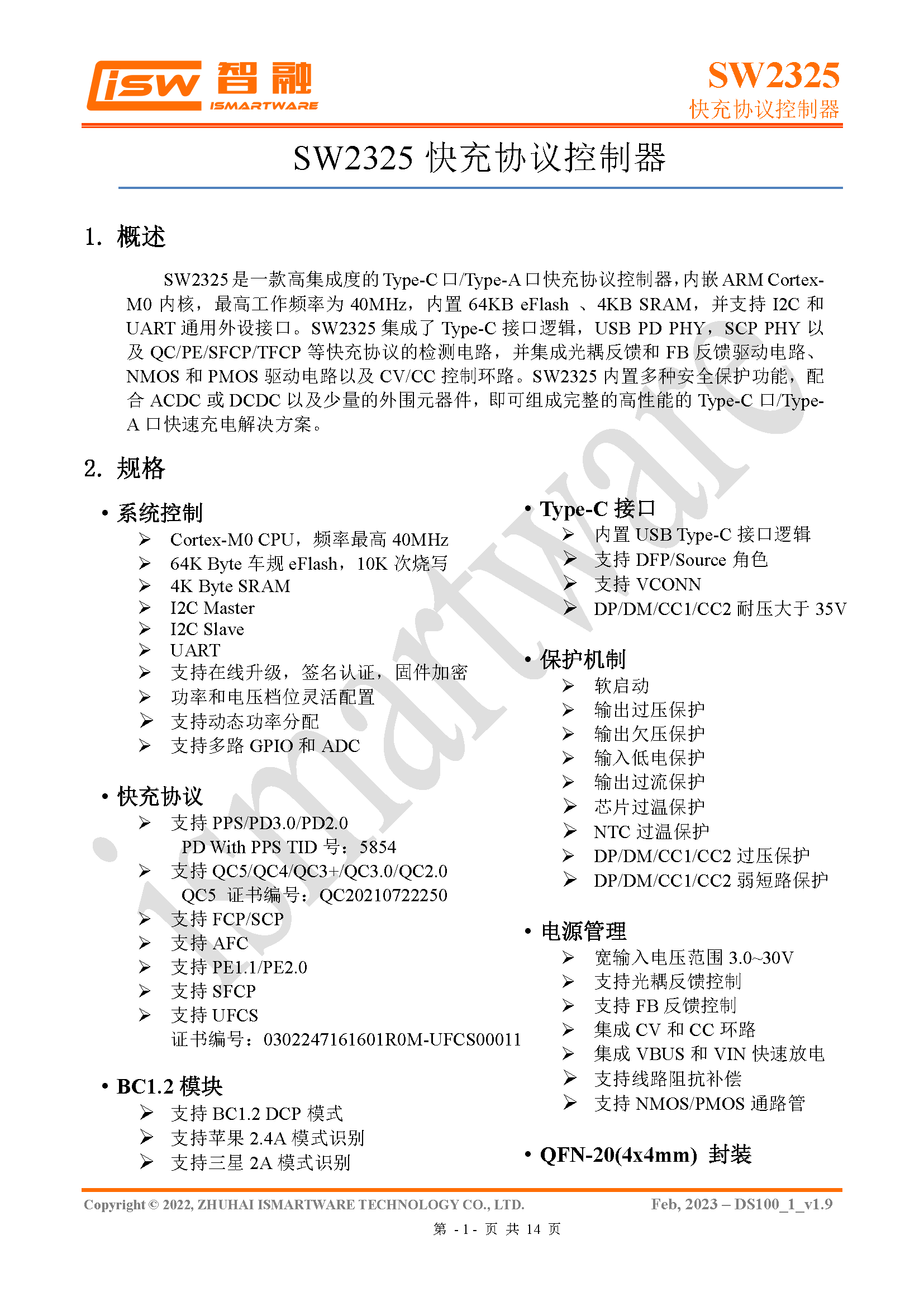
Here is all the information about the iSmartWare SW2325.
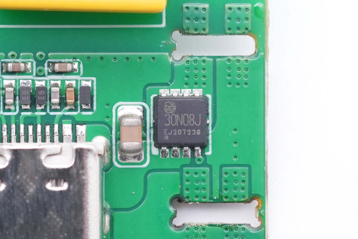
And the output VBUS MOSFET is from HRmicro, model HRT30N08J, it adopts DFN3x3 package. 30V 7mΩ.
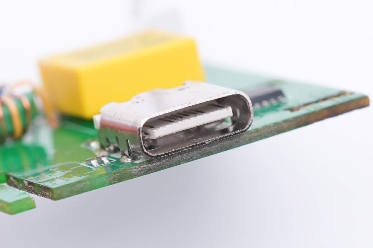
Here is the white USB-C female socket.
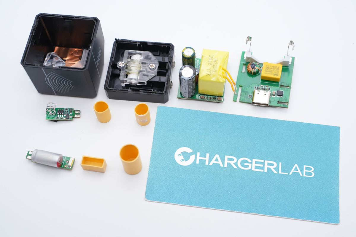
Well, that would be all components of this charger.
Summary of ChargerLAB
Overall, the TEGIC CRYSTAL 35W GaN Charger is very similar to its predecessor on the inside, and it keeps the LED light design, making it still stand out in the charger market. Not only that, it has integrated the previously missing foldable prongs, maximizing space utilization—pretty impressive.
So, if you're looking to purchase a highly portable mini charger for your brand-new iPhone 15 series, this one is definitely worth considering.
Related Articles:
1. TEGIC Launched the NIO Edition 210W GaN Power Station
2. Mcdodo Launched 67W Crystal Series GaN Charger
3. TEGIC Unveils CRYSTAL 35W GaN Charger with Innovative Gemstone-inspired Design

