You can buy it on Amazon: https://amzn.to/39qbkmR
If you wanna buy the tester of POWER-Z, you can visit our Amazon store: Click here.
Introduction
---------------------------------------------------------------
ChargerLAB has taken apart several chargers from Samsung.
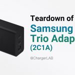
And today, we gonna take apart the brand new 65W trio charger from Samsung.
We find it's composed of two parallel circuits, 35W and 35W, respectively.
Most of the components of those two circuits are the same.
So, the power distribution strategy will be complicated.
Bill of materials (BOM)
------------------------------------------
Time-delay Fuse: Better Electronics (2.5A 250V)
Safety X Capacitor: 0.33μF
Discharge Chip: PI CAP200DG
Bridge Rectifier: RDBSW810
Electrolytic Capacitor: Chang electronics, CapXon
Master Control Chip: PI SC1920C
SMD Y Capacitor: Anshan Keifat
Synchronous Rectifier: China Resources Micro CRSM055N10L2
Solid Capacitor: CapXon
MOSFET: SAST WTM303P080LS-AH
Protocol Chip/MCU: ABOV A94B458LUN
Output VBUS MOSFET: Winning Team SFTN7422SMP-HAF
Synchronous Buck-boost Converter: Southchip SC8721
Related Articles:
1. Teardown of Samsung 45W GaN Charger EP-T4510 (US Version)
2. Teardown of Samsung 25W USB-C Fast Charger (EP-TA800)
3. Teardown of Samsung 45W USB-C Fast Charging Wall Charger

