Introduction
Samsung has recently introduced a dual port charger, model TA220, that delivers 35W of power. This charger is equipped with one USB-C port and one USB-A port. The USB-C port delivers up to 35W of power when used alone, while the USB-A port offers up to 15W of power output. If both ports are utilized simultaneously, the USB-C port will drop to 20W while the USB-A port remains at 15W.
This charger is compatible with both Android and Apple devices, making it an ideal solution for charging laptops, tablets, and smartphones. With its excellent compatibility with mainstream devices, let's now take a closer look at the internal components and structure of this device.
Product Appearance
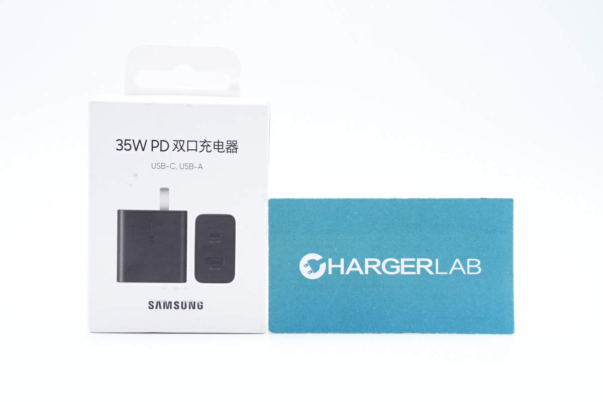
The front of the packaging box for the Samsung charger features a minimalist design style, simply displaying the Samsung brand, charger appearance, and name.
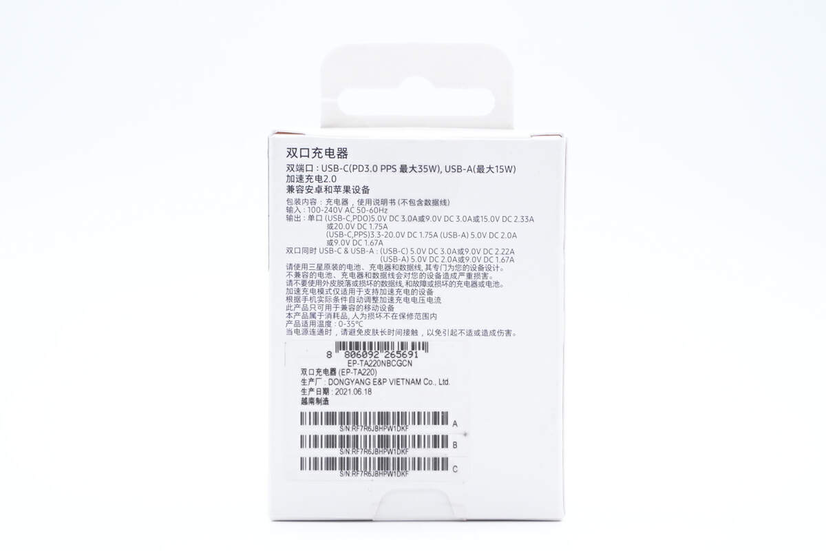
On the back of the packaging, you will find the charger's specifications and precautions.
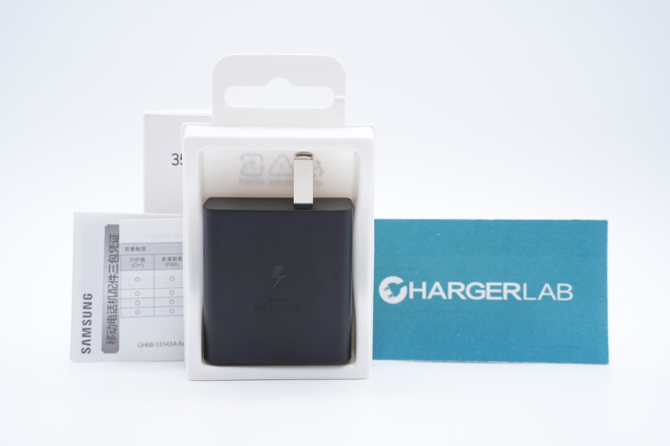
The package contains the charger, instructions, and a list of toxic and hazardous substances.
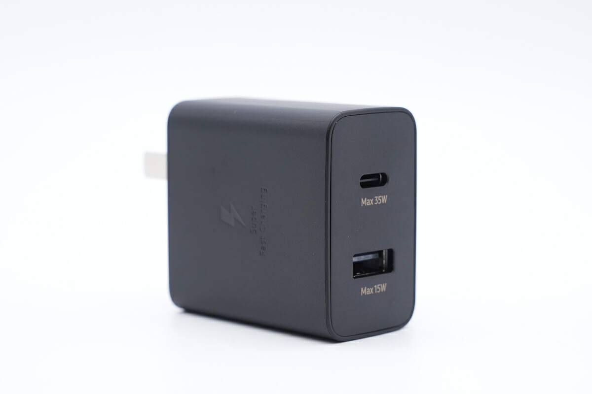
The charger retains the classic Samsung fast-charging style, featuring a matte finish and fingerprint-resistant shell.
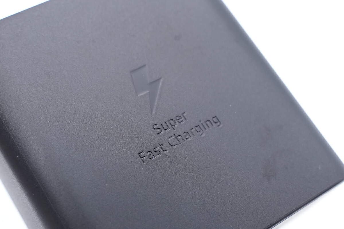
The "Super Fast Charging" is on the front of the charger.
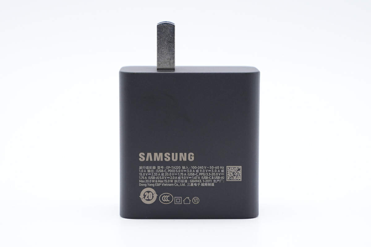
And all specs info are on the back.
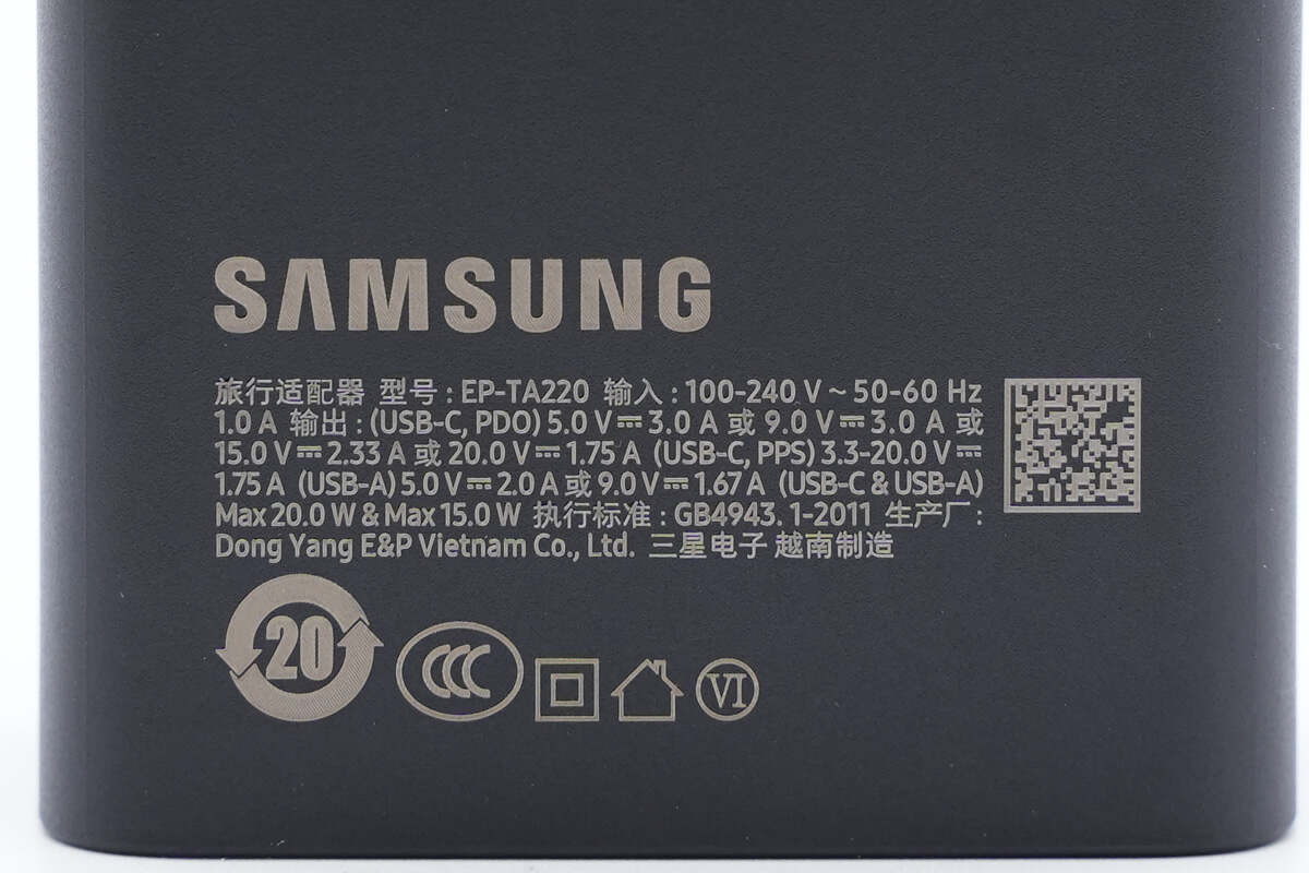
Model is EP-TA220. It supports input of 100-240V~50/60Hz 1.0A. The USB-C can support up to 35W, while the USB-A only supports up to 15W. When charging two devices, the power will be divided into 20W and 15W.
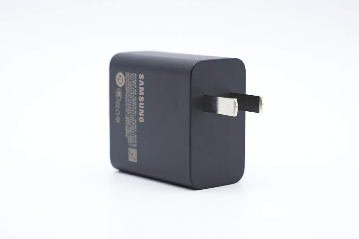
It's a pity that it still adopts fixed input prongs.
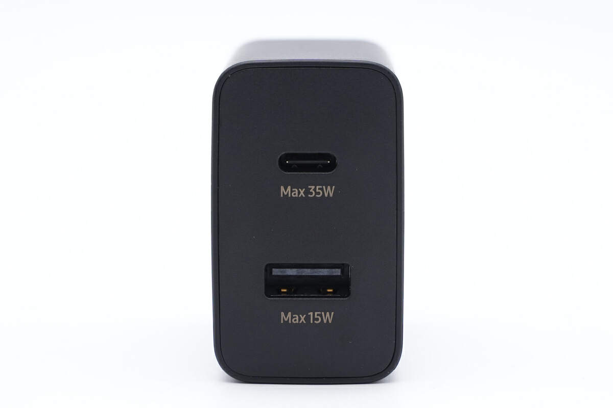
Here is the output panel, it's equipped with a USB-C and a USB-A port.
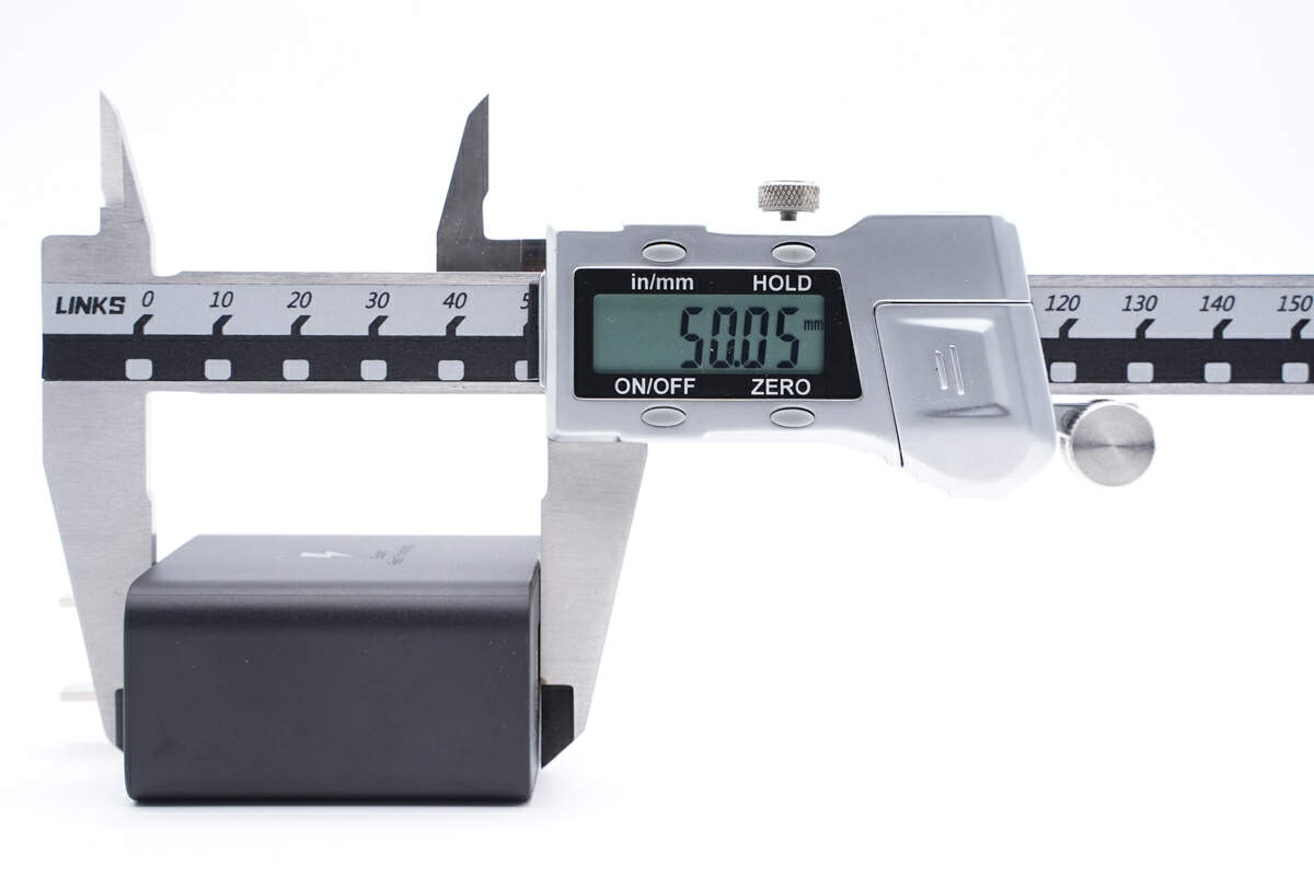
The length of the charger is about 50mm (1.97 inches).
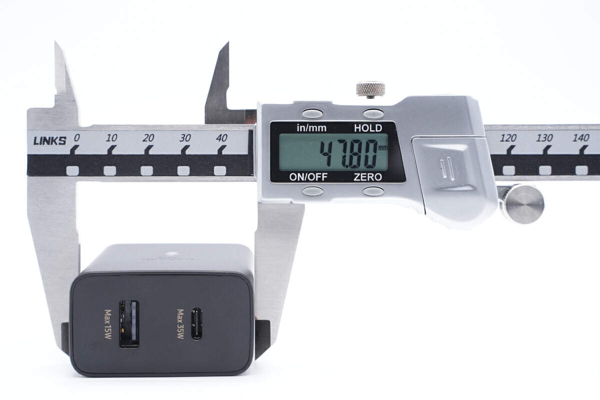
The width is about 47.8mm (1.88 inches).
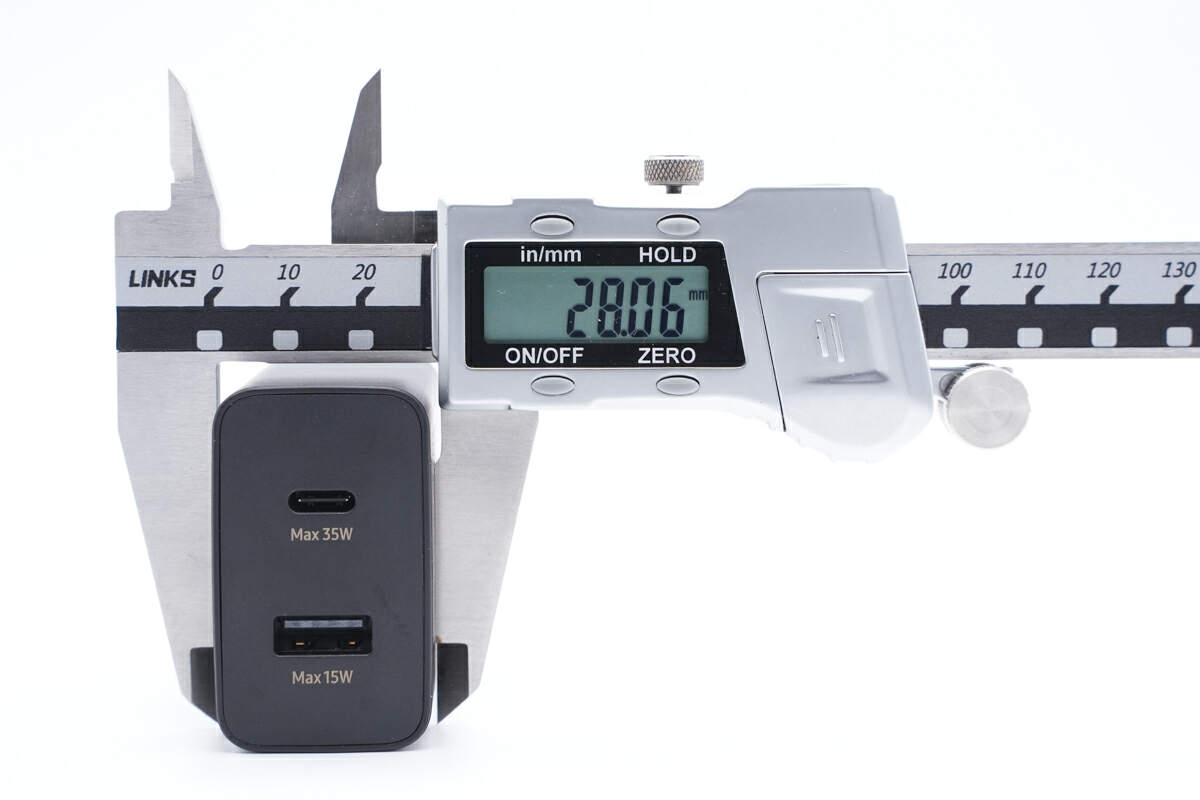
And the height is about 28.1mm (1.11 inches).
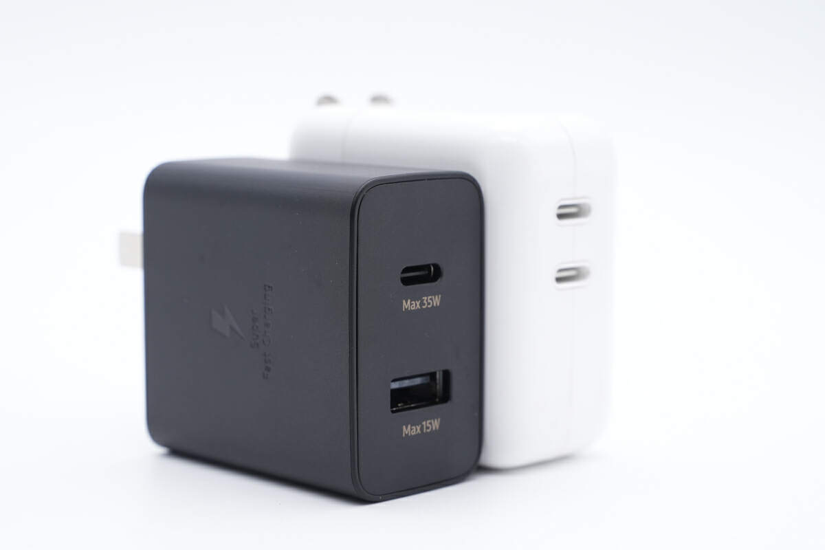
Compared with Apple 35W dual USB-C charger, it's slightly smaller.
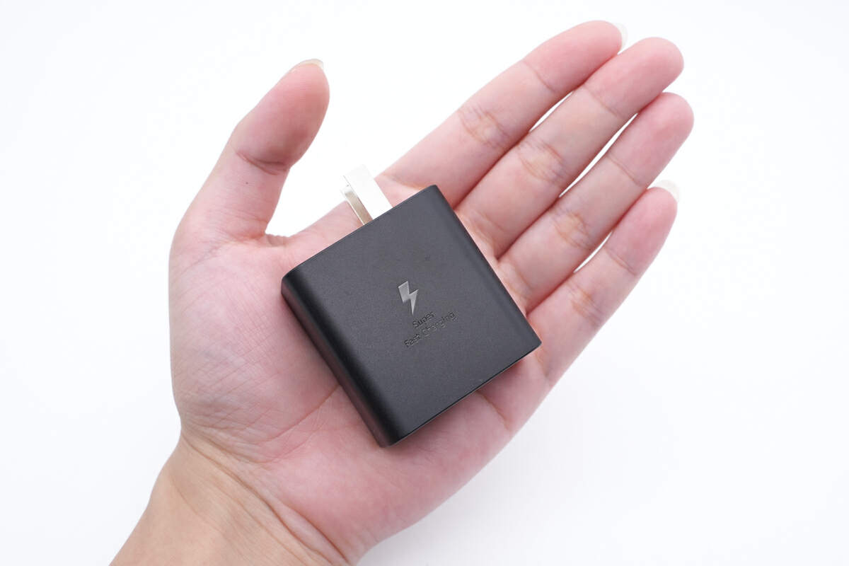
This is how it looks like on my hand.
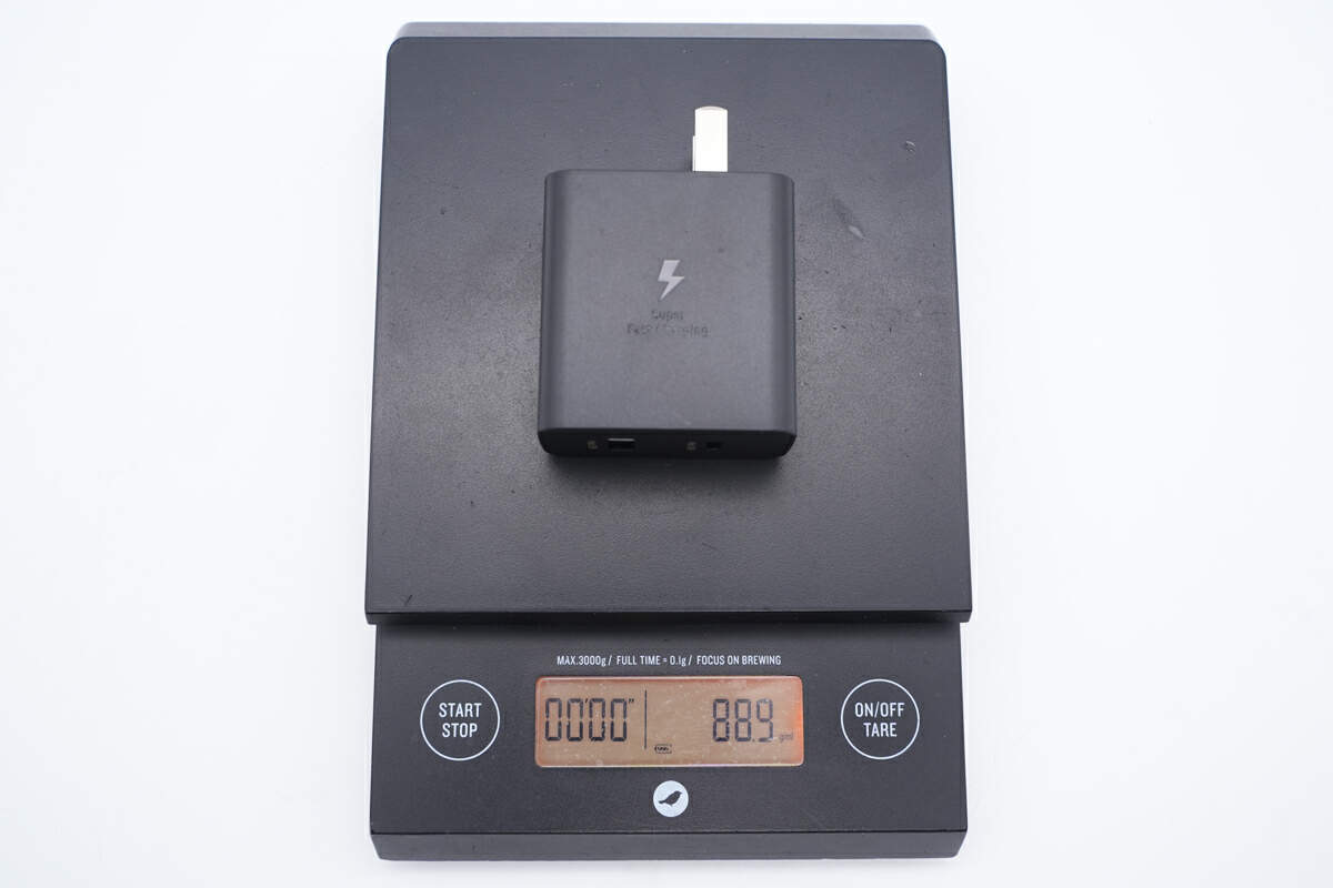
And the weight is about 89g (3.14 oz).
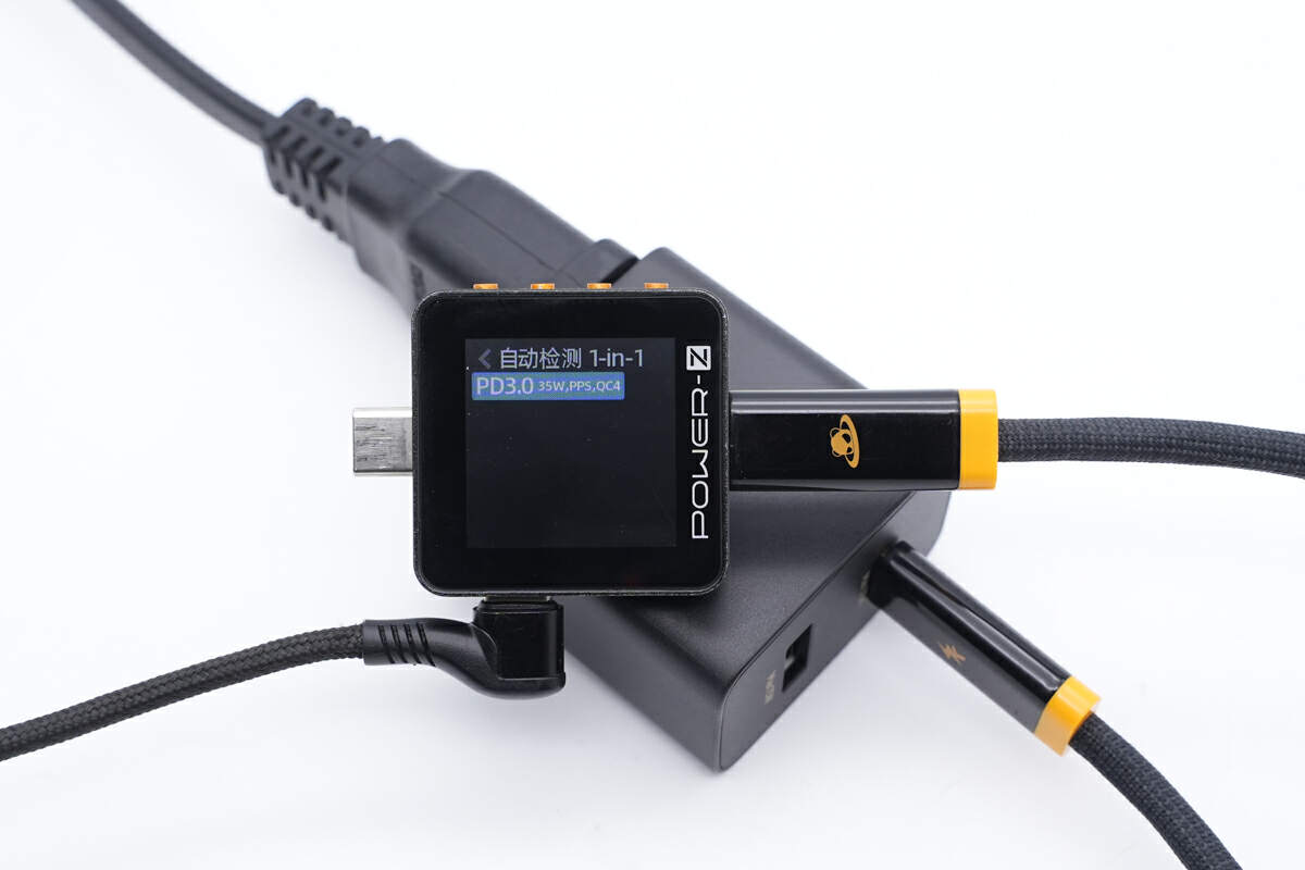
The ChargerLAB POWER-Z KM002C shows the USB-C supports PD3.0, PPS, QC4 protocols.
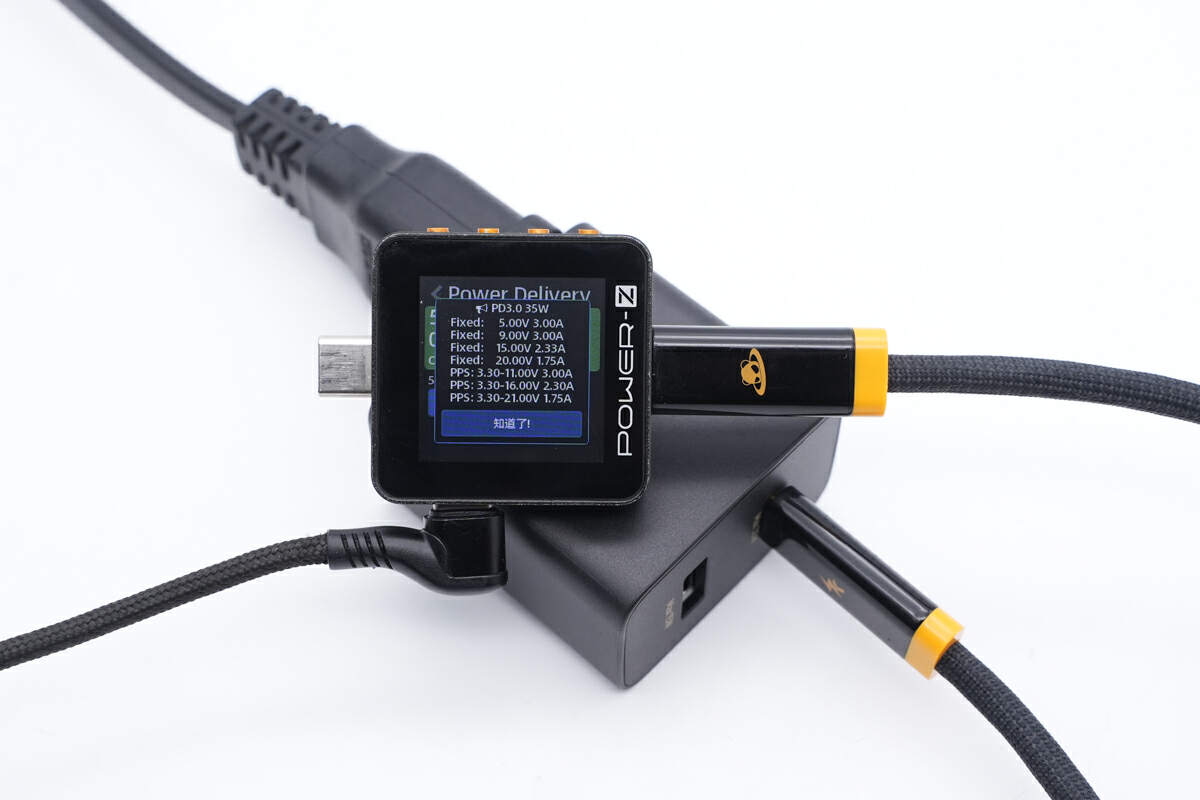
And it also supports four fixed PDOs of 5V/9V3A, 15V2.33A, 20V1.75A, and three sets of PPS.
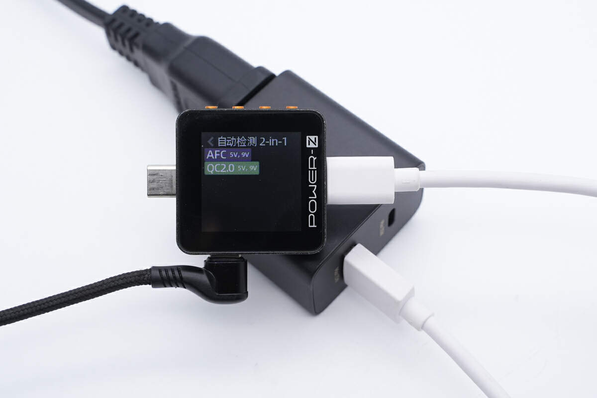
The USB-A only supports AFC and QC2.0 protocols.
Teardown
Now that we have completed our unboxing and testing of Samsung's charger and gained a fundamental understanding of its size and performance, it's time to take apart the device and examine its internal components and structure.
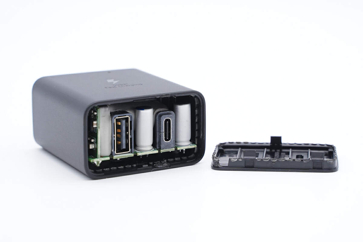
Use the spudger to pry along the gap and remove the top case.
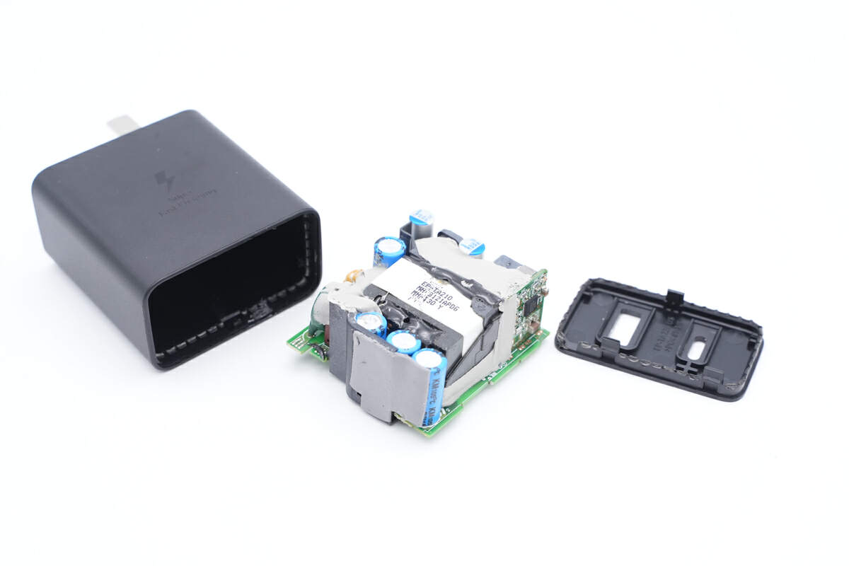
The internal PCBA module can be easily pulled out.
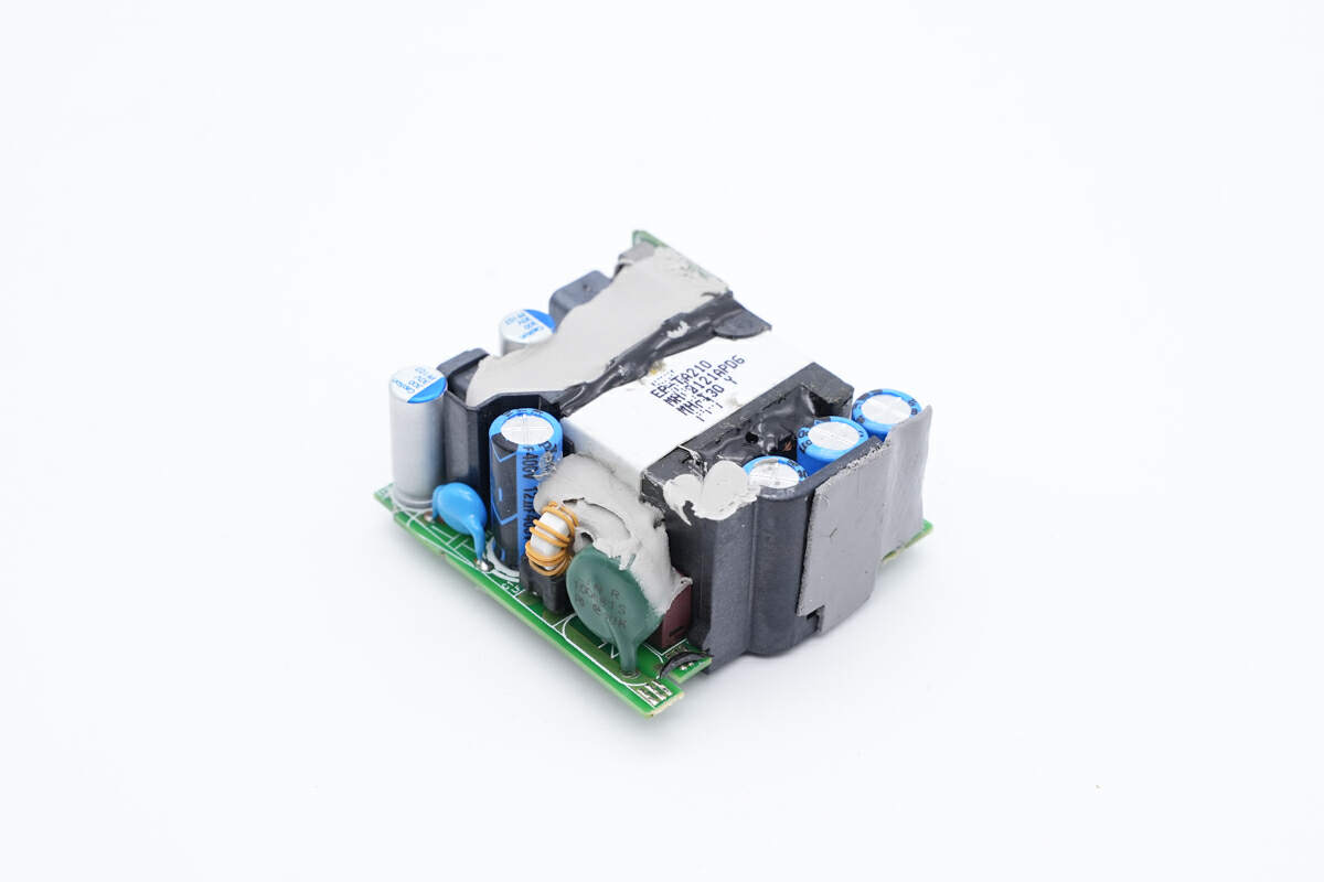
The transformer is fixed by silicone adhesives.
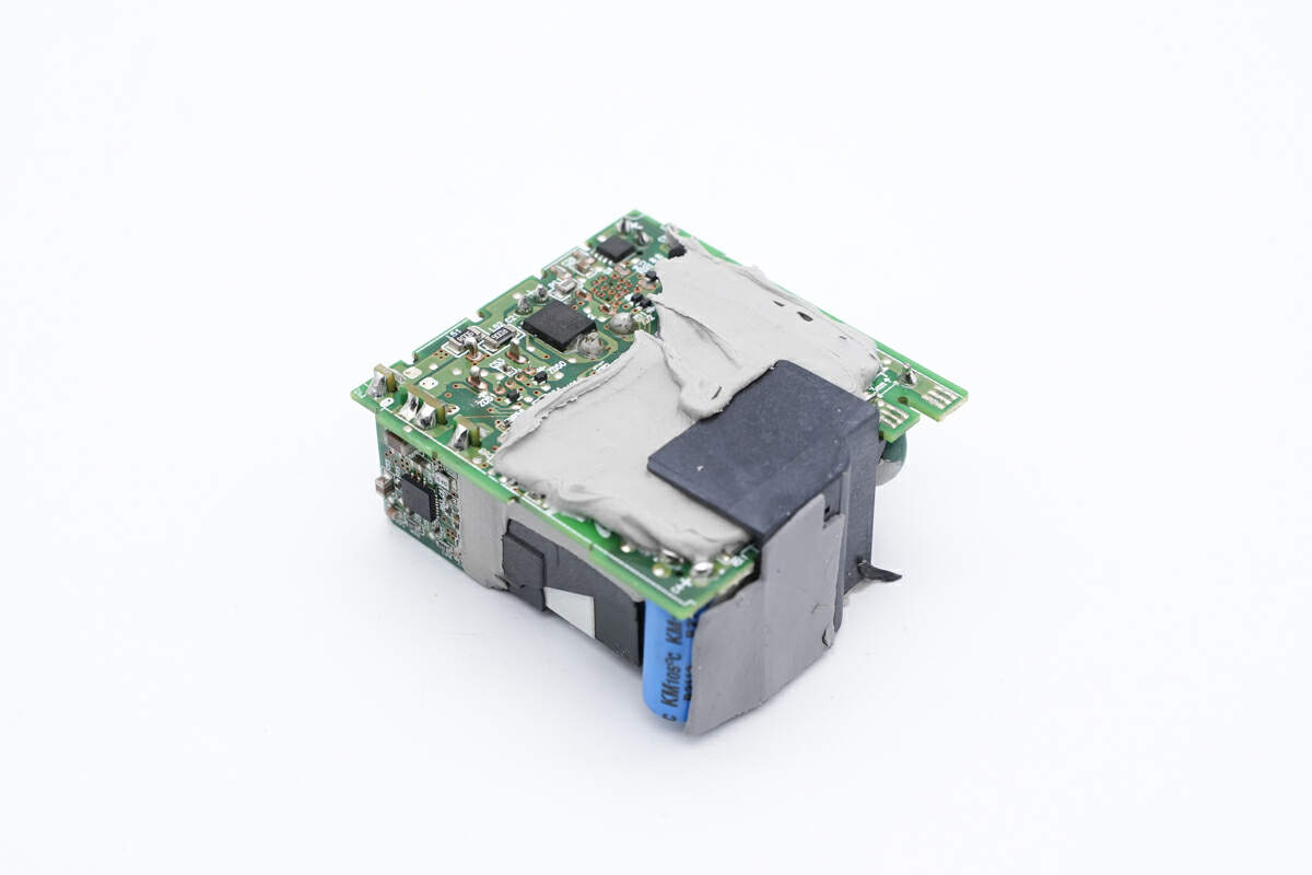
And the adhesives can also be seen on the back.
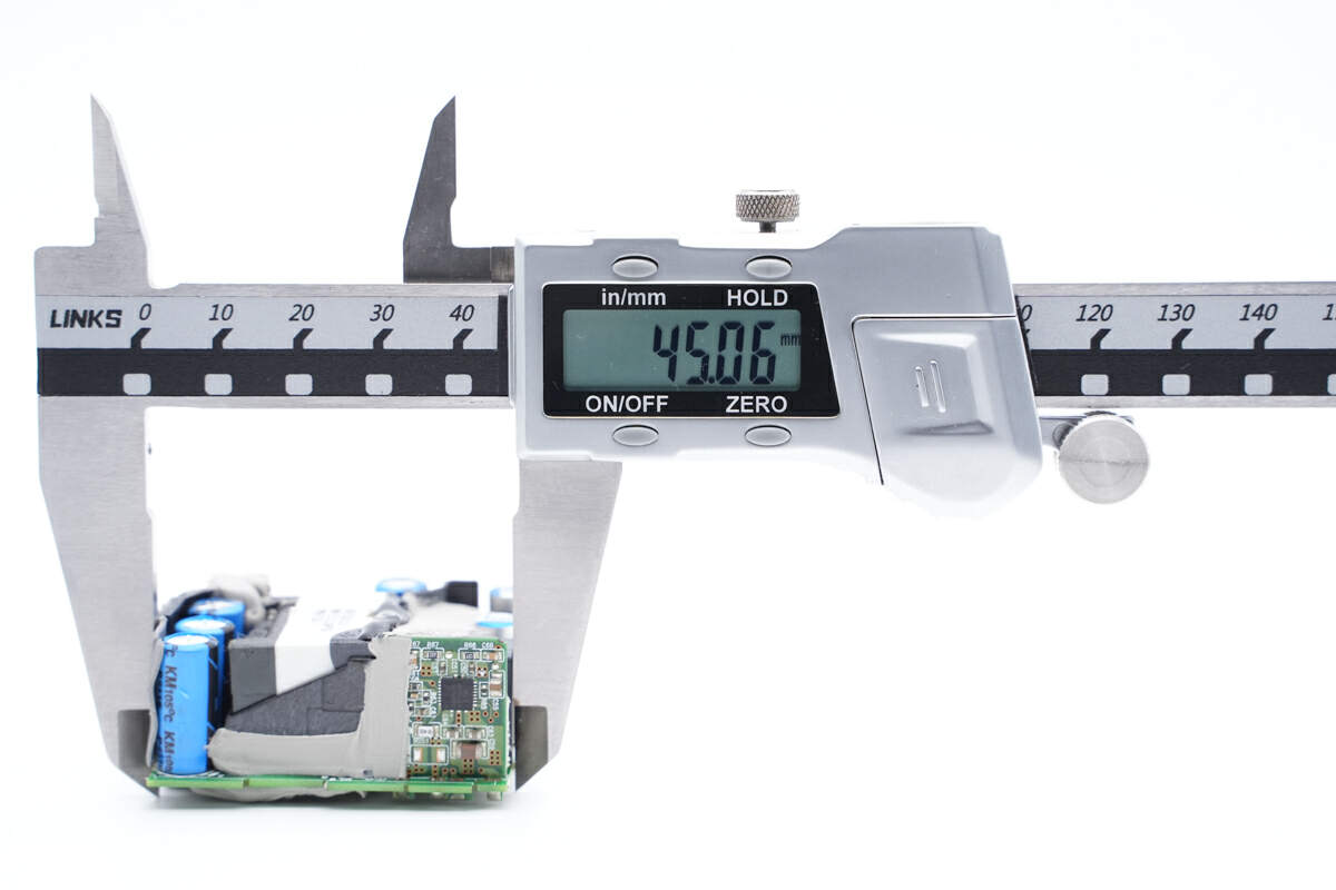
The length of the PCBA is about 45.1mm (1.78 inches).
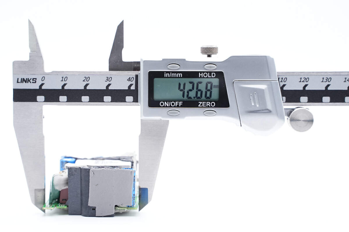
The width is about 42.7mm (1.68 inches).
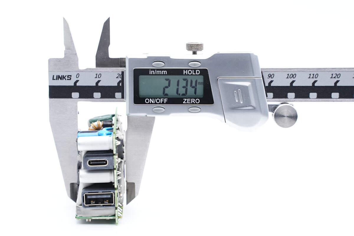
And the height is 21.3mm (0.84 inches).
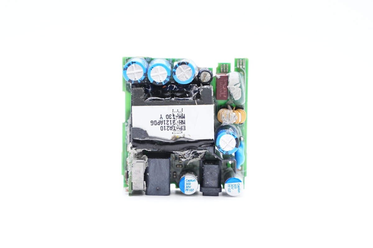
The fuse, varistor, high-voltage filter capacitor, and transformer are located on the front of the PCBA module.
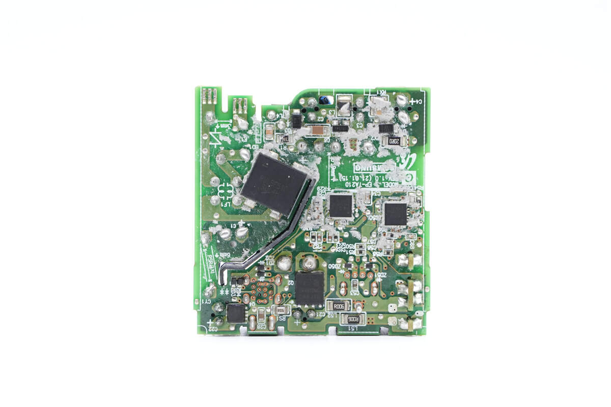
And ChargerLAB found it adopts traditional QR flyback topology. The current will be filtered by synchronous rectification circuit for output. The groove is inserted into the isolation plate, which is obvious. The isolation plate is inserted into the groove, which can insulate the primary and secondary sides.
Then, let's start from the input end.
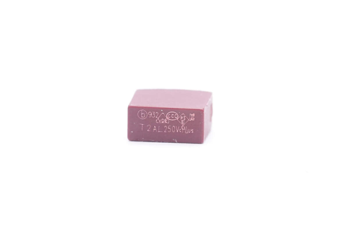
The input time-delay fuse is from Better Electronics. 2A 250V.
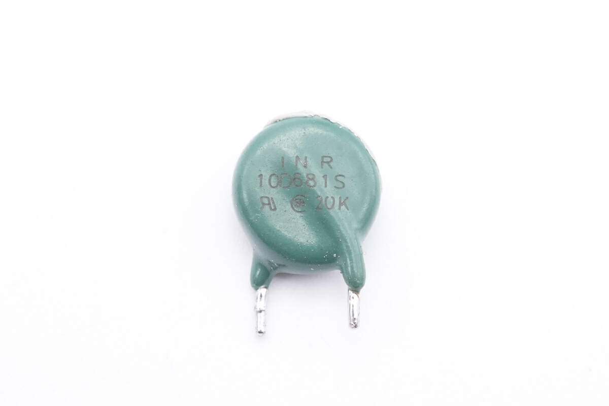
The green varistor marked with INR10D681S is used for input surge and overvoltage protection.
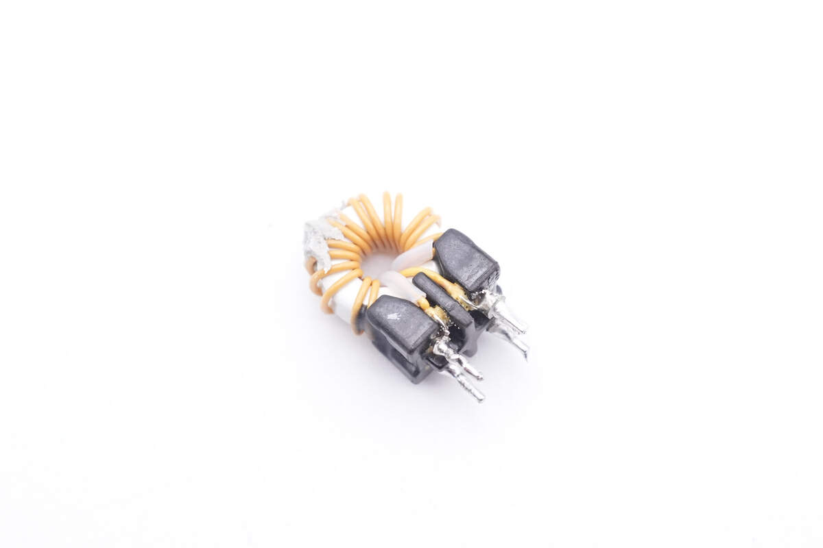
The common mode choke is wound with insulated wires.
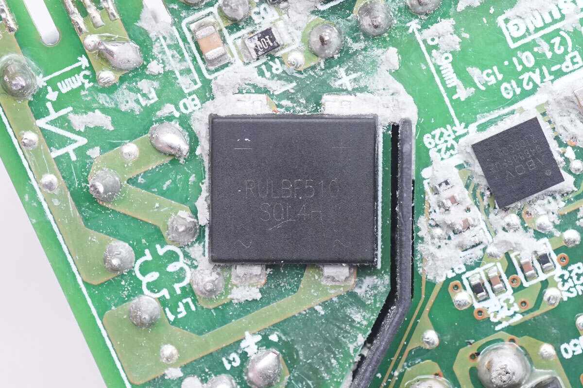
The bridge rectifier is marked with RULBF510.
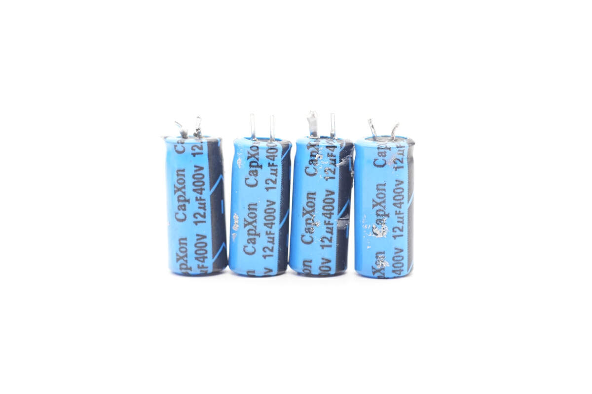
A total of 48μF, consisting of four blue CapXon electrolytic capacitors connected in parallel, with each capacitor being rated at 12μF and 400V.
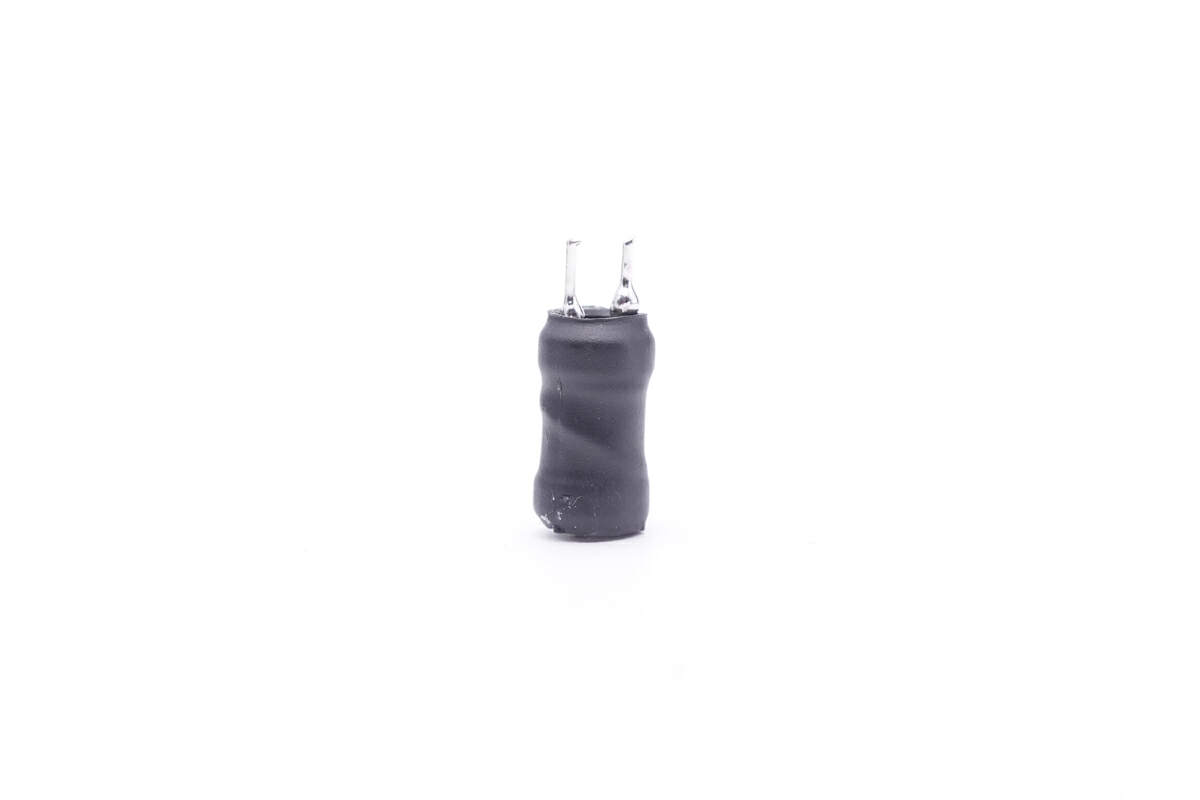
The differential mode choke adopts I-shaped magnetic core.
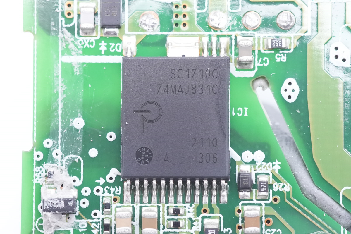
The power IC is soldered under the transformer and is from PI InnoSwitch3-Pro series. It integrates primary PWM controller, primary MOSFET, secondary synchronous rectification controller, etc. The high integration makes the charger smaller. And the model is SC1710C.
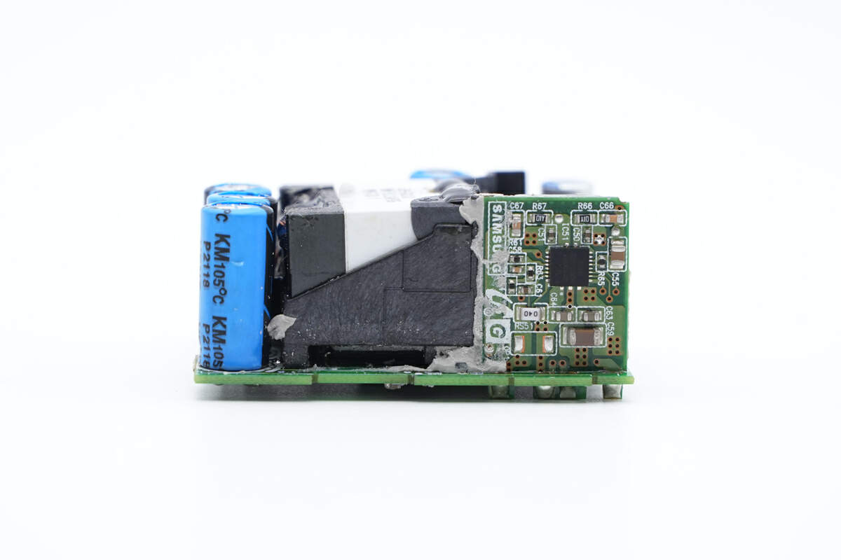
On the side of the PCB, you will find the high-voltage filter capacitor, transformer, and buck-boost small PCB.
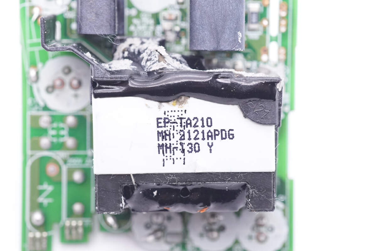
And the transformer is marked with EP-TA210.
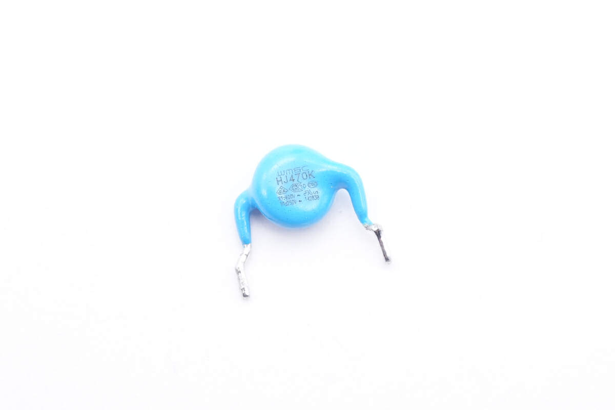
The blue Y capacitor is from WMEC, which has two shorter pins.
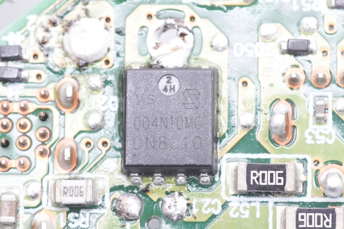
The synchronous rectifier is from Vergiga Semi and adopts PDFN5060X package. Ane the model is VSP004N10MS-G. 100V 3.8mΩ.
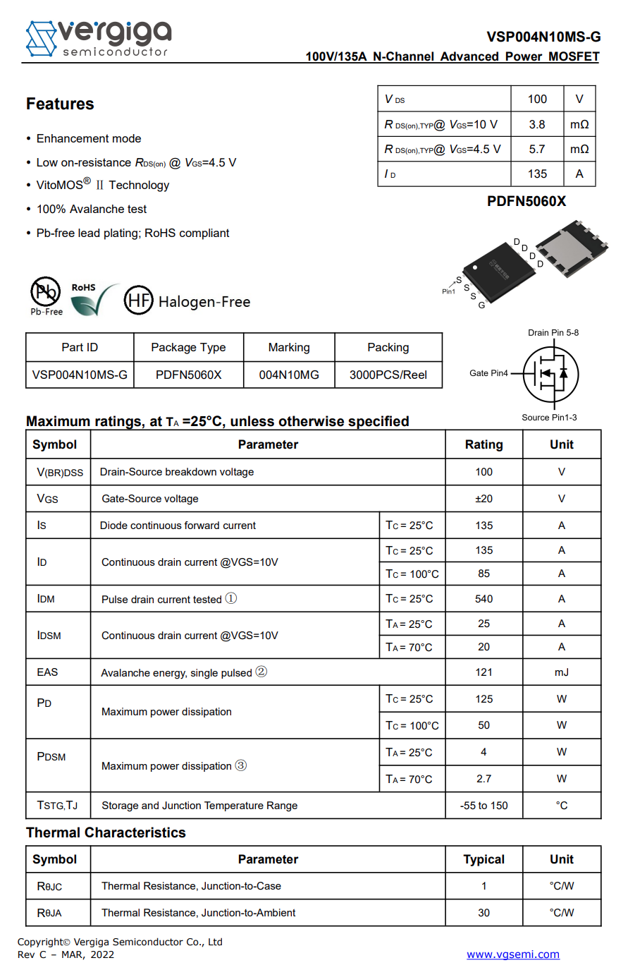
Here is all the information about Vergiga Semi VSP004N10MS-G.
ChargerLAB has discovered that MOSFETs from Vergiga Semi are being utilized across a range of industries, including chargers, wireless chargers, car chargers, power banks, and portable power stations. These MOSFET components are present in dozens of popular products produced by industry giants like Huawei, Xiaomi, Zimi, Samsung, OPPO, VIVO, Meizu, Nubia, Baseus, and Bull. Customers consistently recognize the high quality of these products.
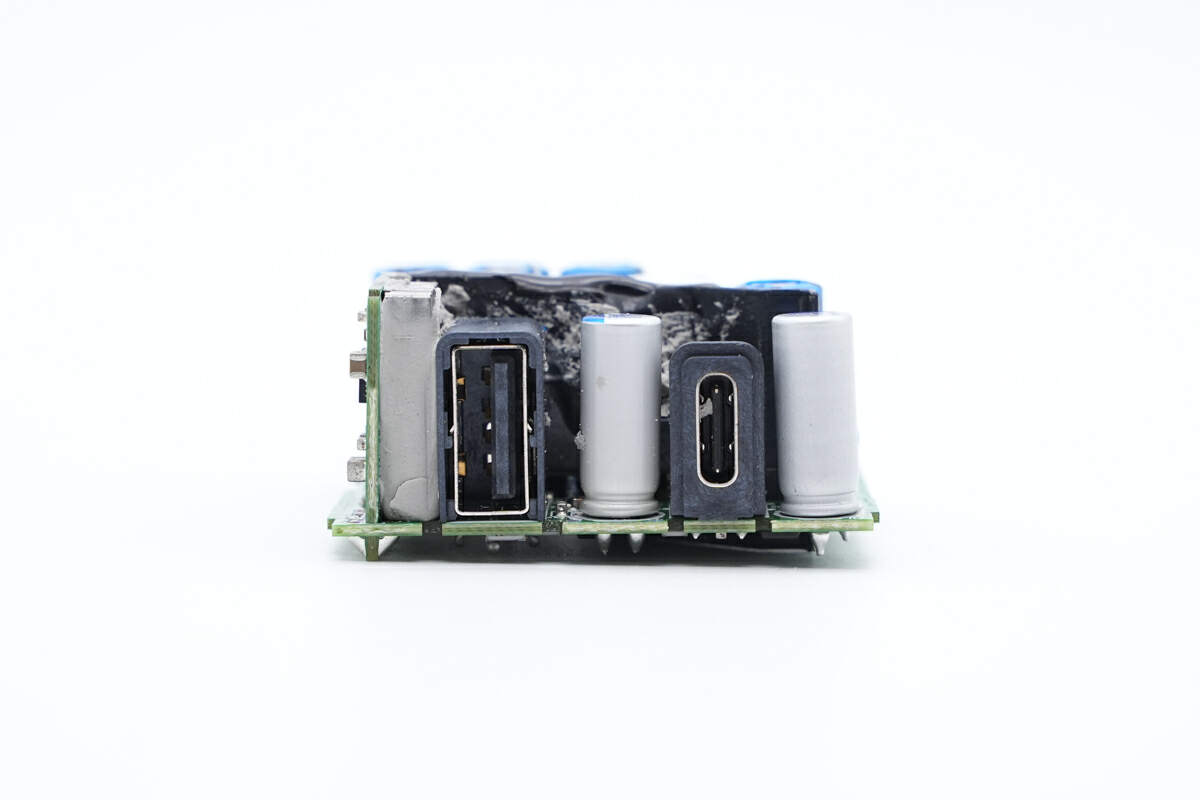
The buck-boost small PCB, USB-A socket, solid capacitor, and USB-C socket are on this output end.
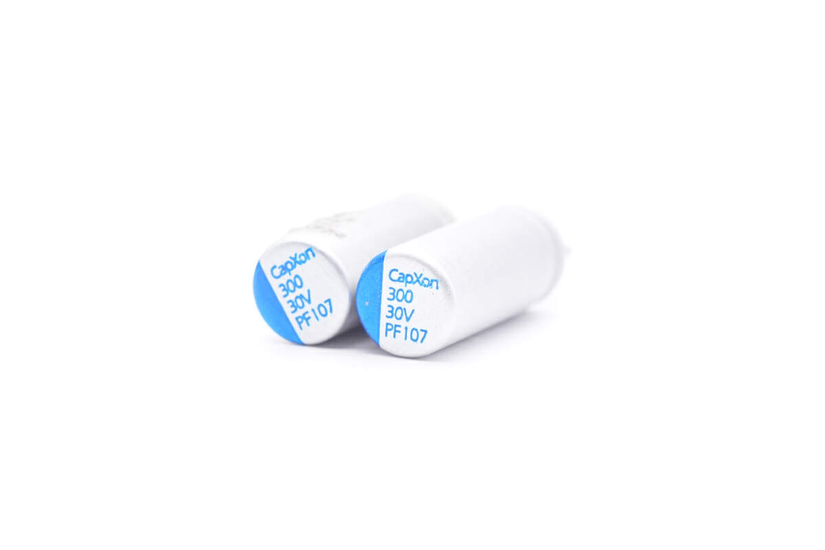
Those two solid capacitors are connected in parallel for output filtering. They're from CapXon PF series. 300μF 30V for each.
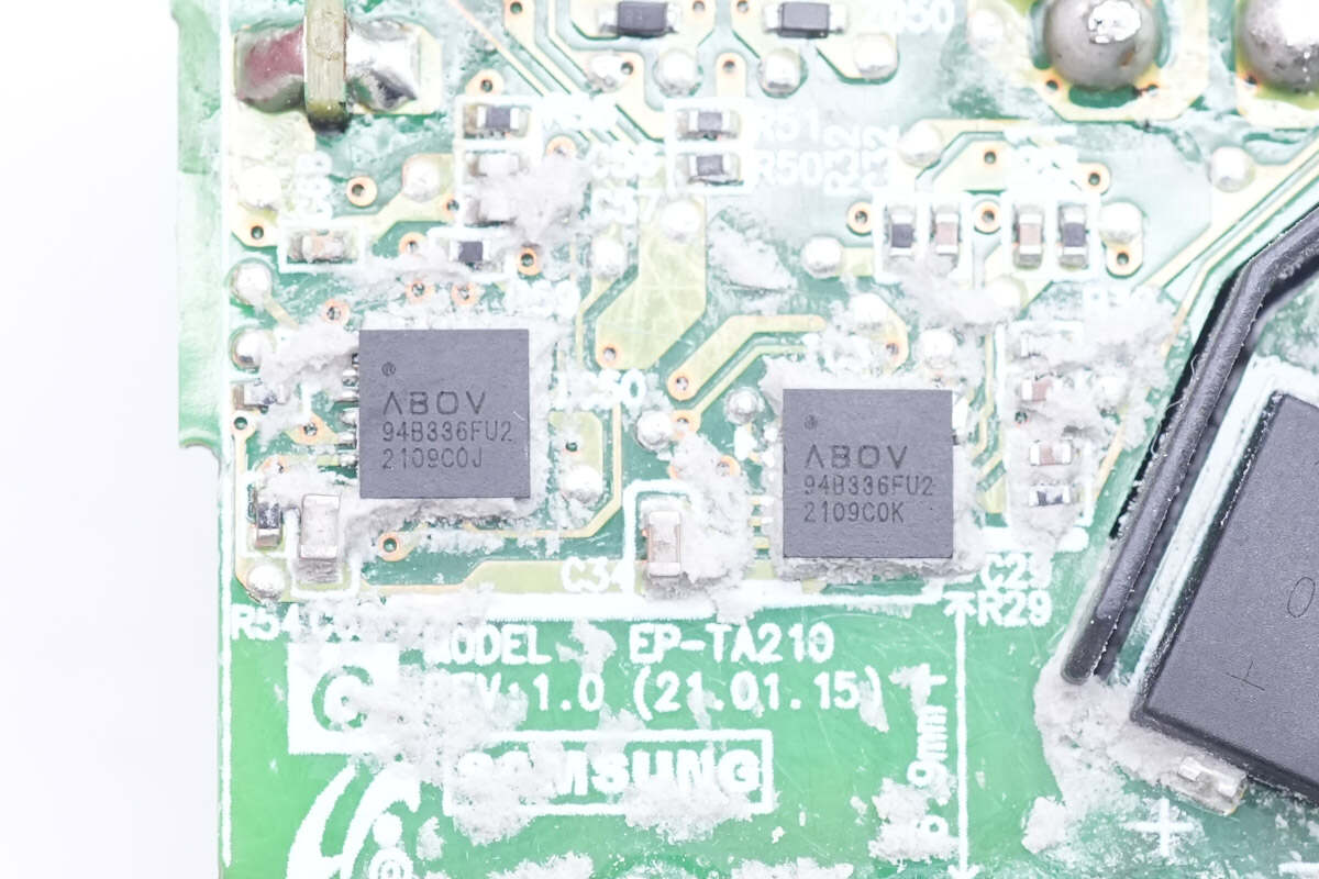
Those two protocol chips are from ABOV and are used to control the USB-C and USB-A ports, respectively. It integrates 8051 core and 16KB flash.
Withstand voltage is 30V. And the model is A94B336.
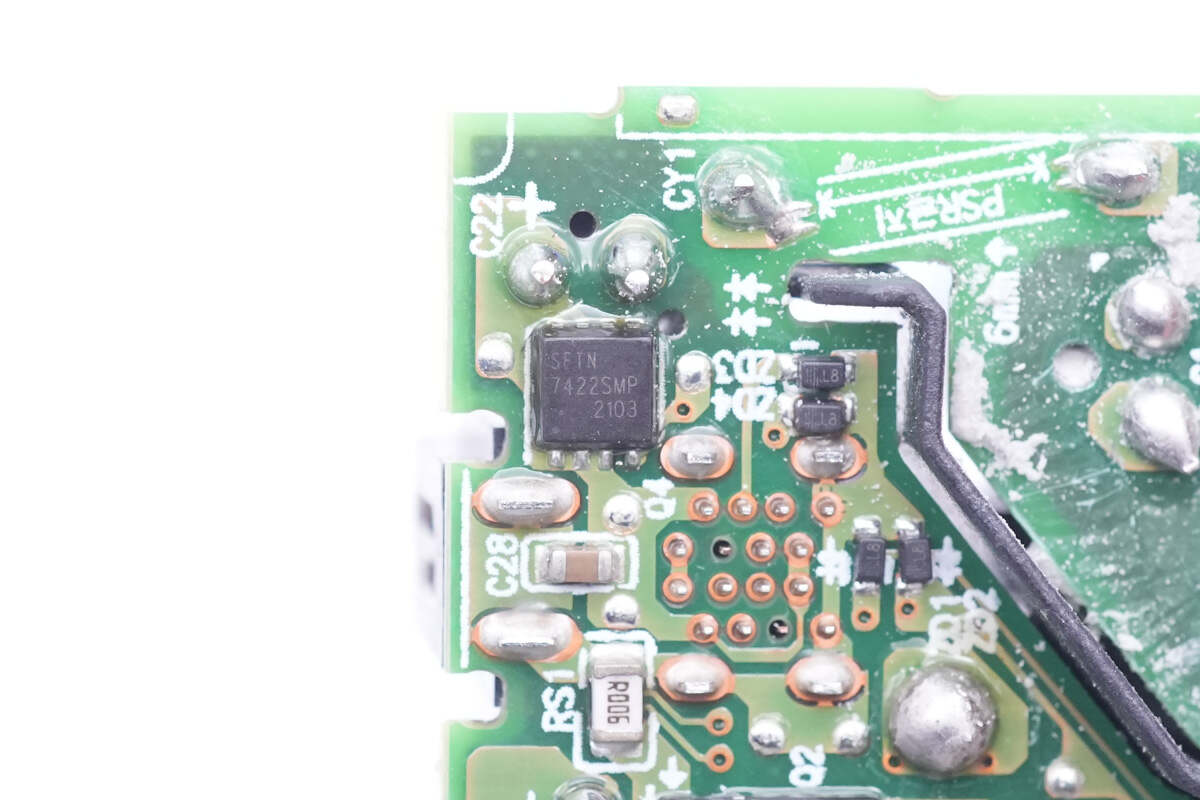
The output VBUS MOSFET of USB-C port is from Winning Team and adopts DFN3030 package. Model is SFTN7422SMP. 30V 4mΩ.
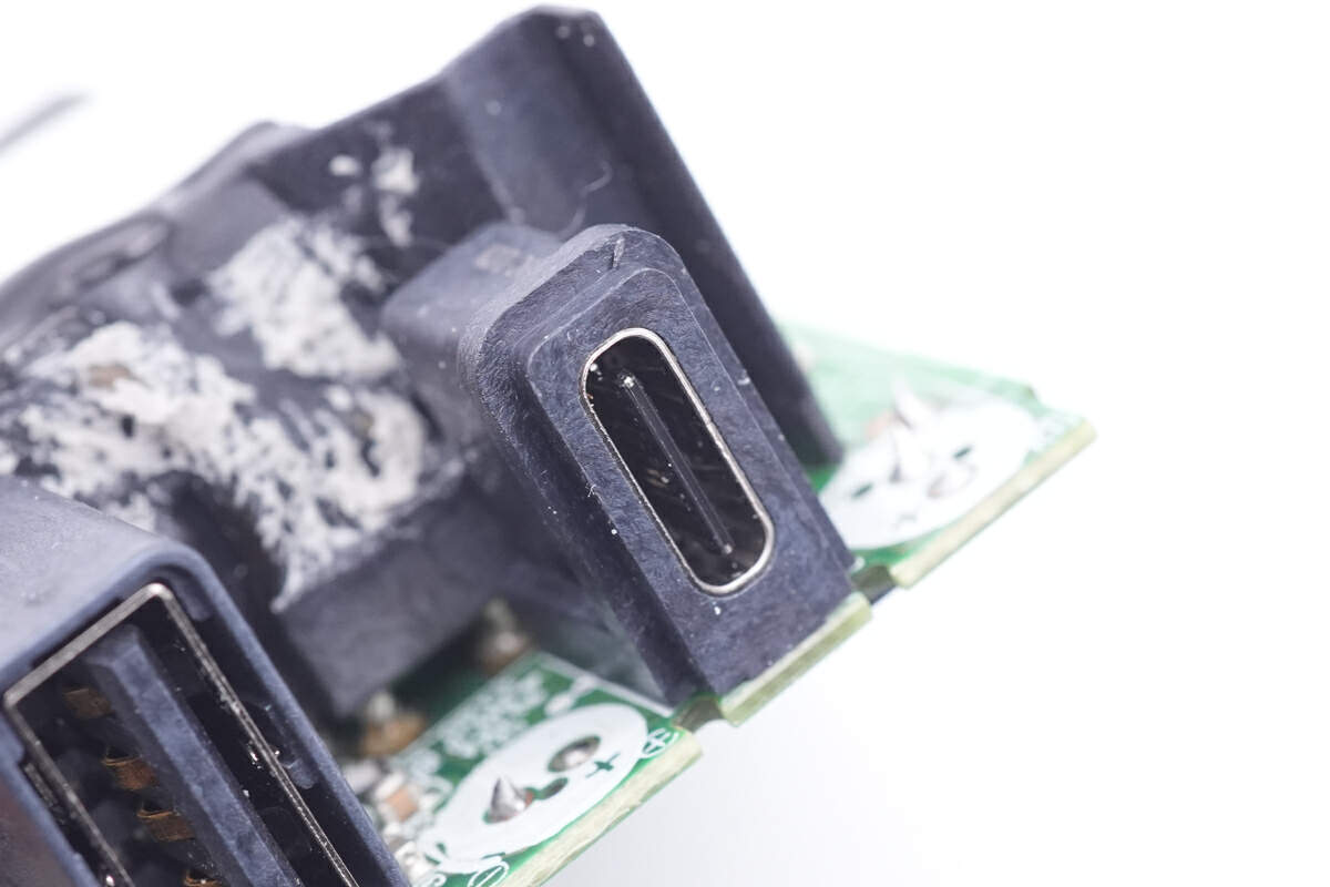
The plastic sheet inside the USB-C socket is black.
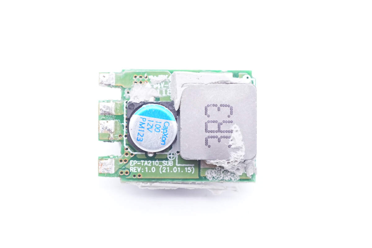
An alloy inductor and a solid capacitor for output filtering are on the front of the buck-boost small PCB.
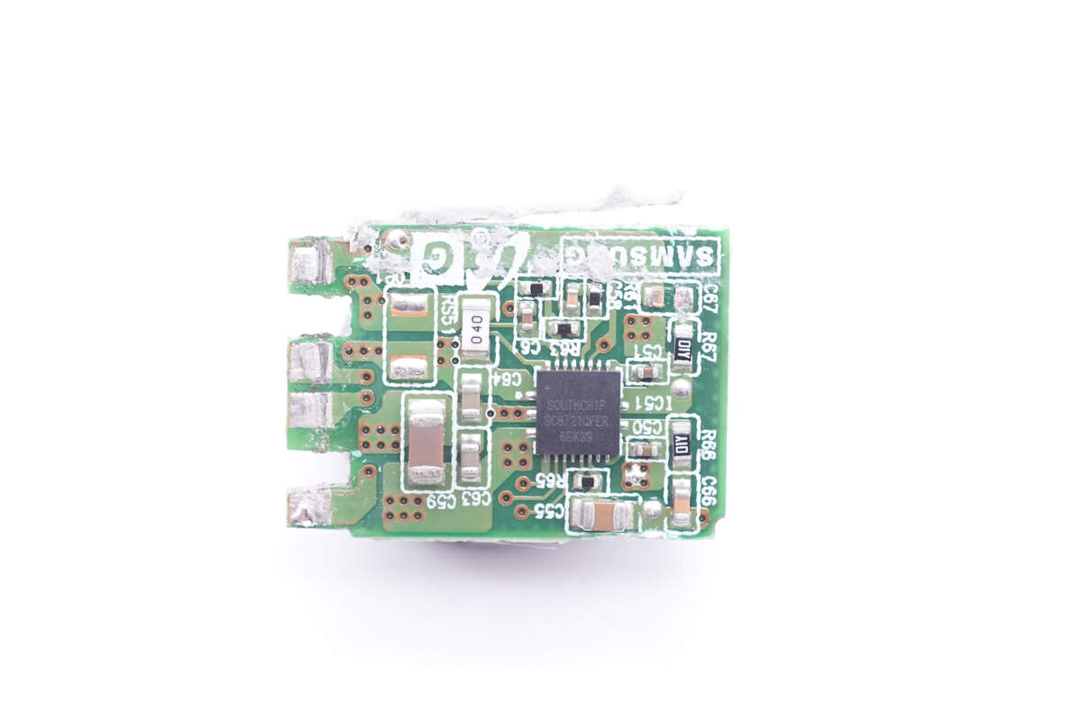
And a synchronous buck-boost converter is on the back.
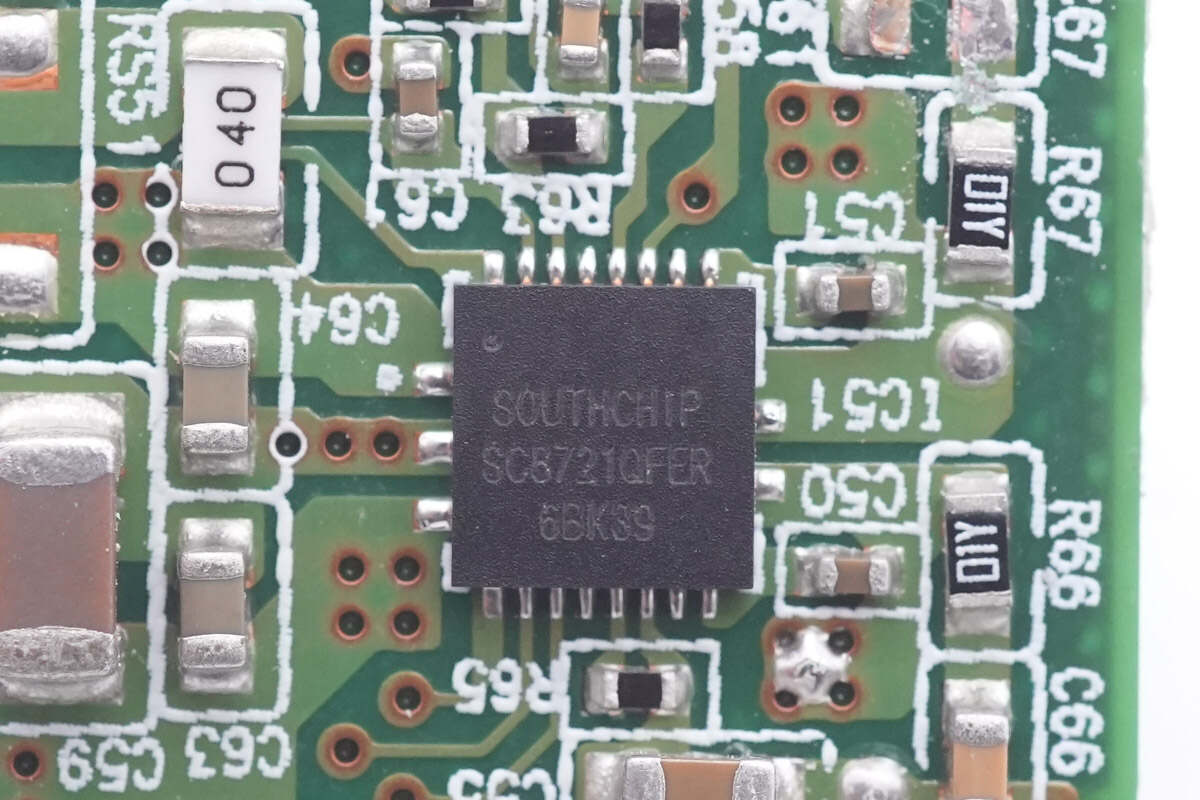
And the synchronous buck-boost converter of USB-A is from Southchip. It integrates four buck-boost MOSFETs to form an H-bridge, the input and output voltage is between 2.7-22V. It also supports wide input and output voltage range, output
current limit, dynamic output voltage adjustment, internal current limit, output short protection and over temperature protections to ensure safety under different abnormal conditions. And the model is SC8721.
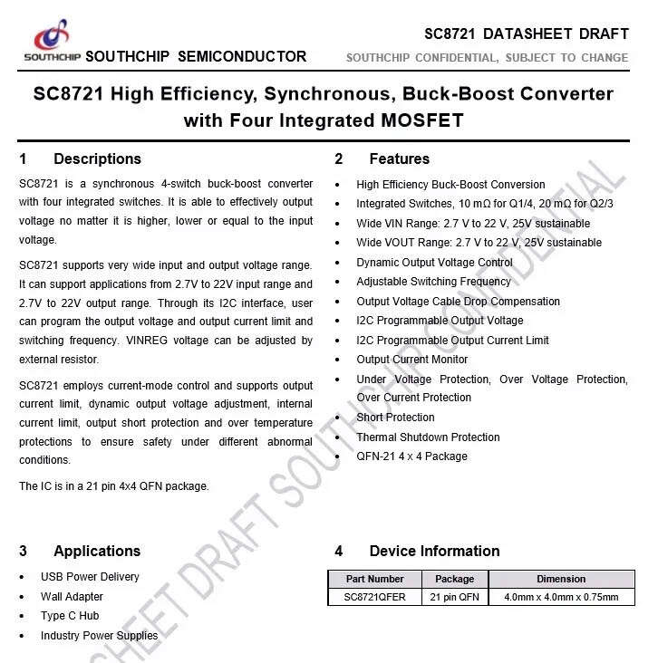
Here is all the information about Southchip SC8721.
ChargerLAB also learned that there are other products that use this chip, including Anker 25600mAh power bank, Nubia Red Magic 45W USB PD power bank, Xiaomi 20000mAh power bank, and Thinkplus 14000mAh 45W PD fast charging power bank.
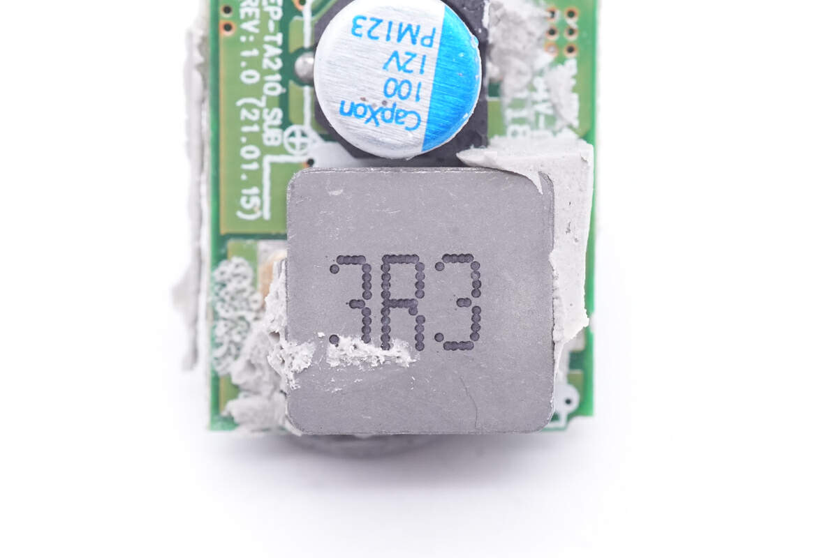
Here is a 3.3μH alloy inductor.
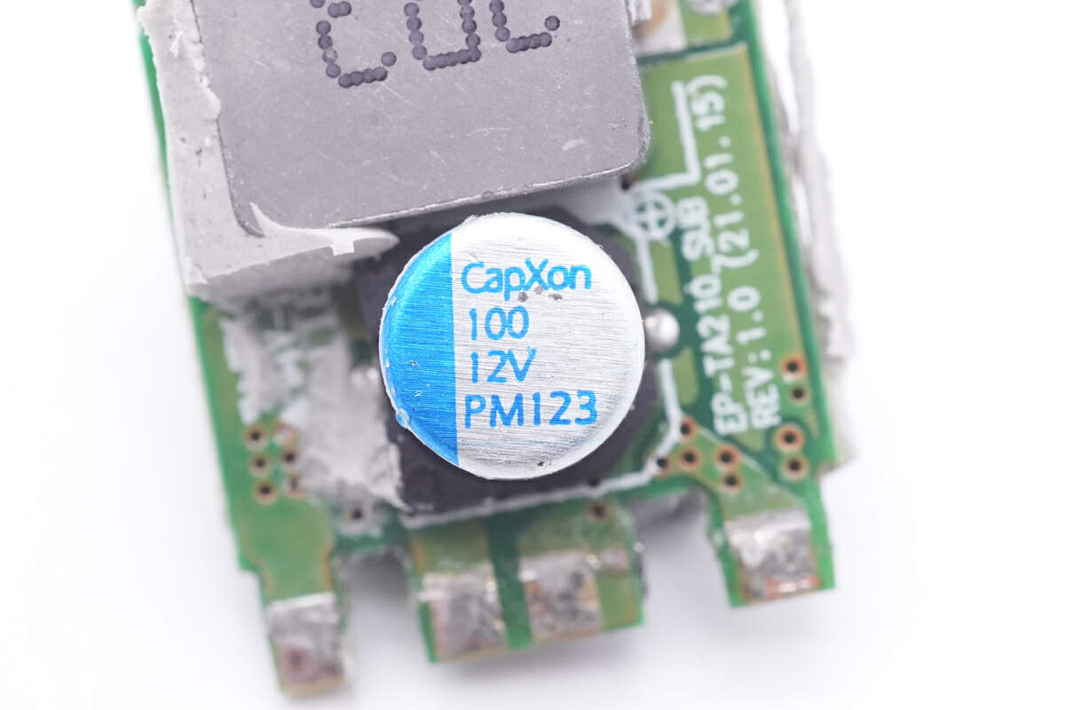
This solid capacitor is soldered on the buck-boost PCB of USB-A. It's from CapXon PM series. 100μF 12V.
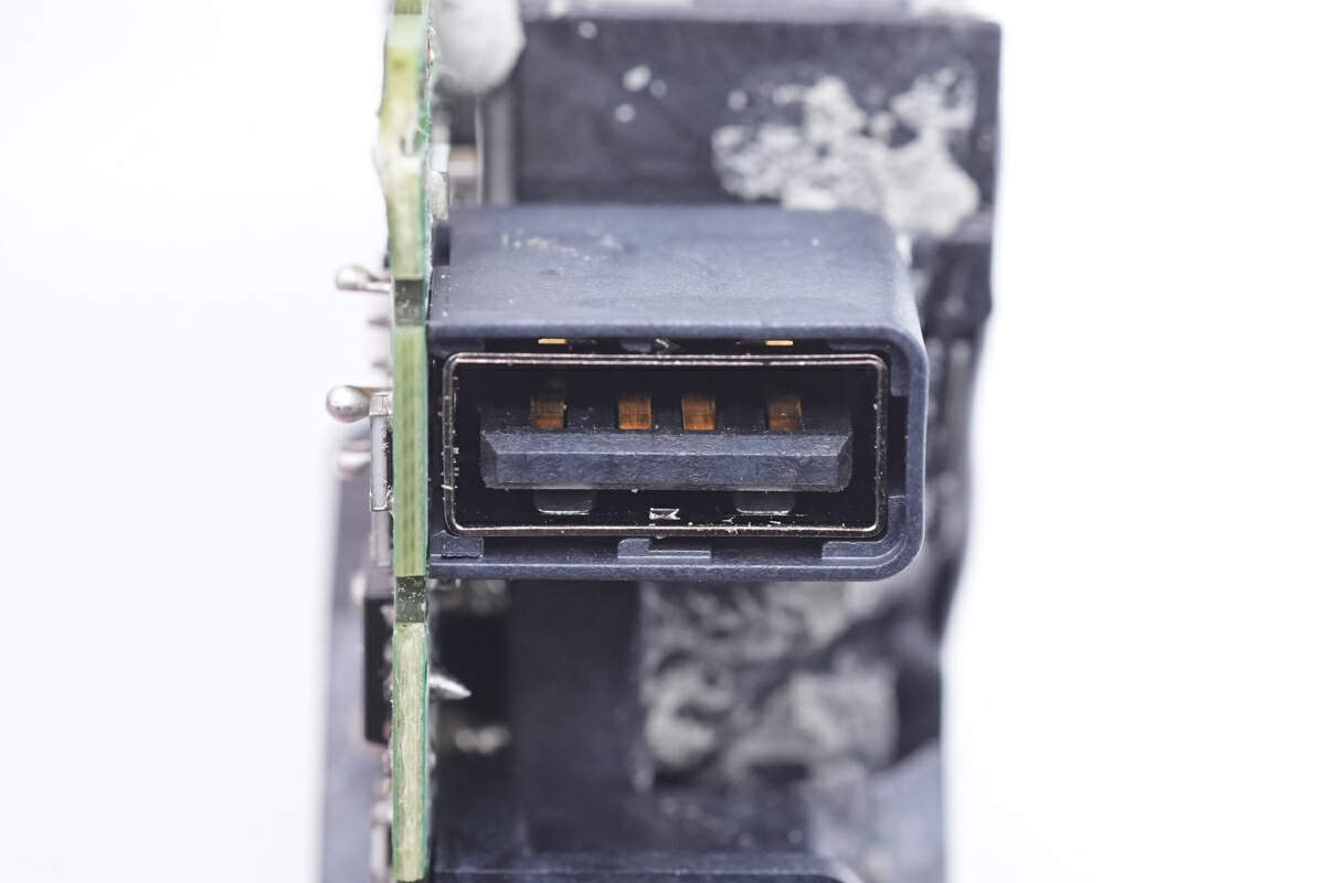
The plastic sheet inside the USB-A socket is black.
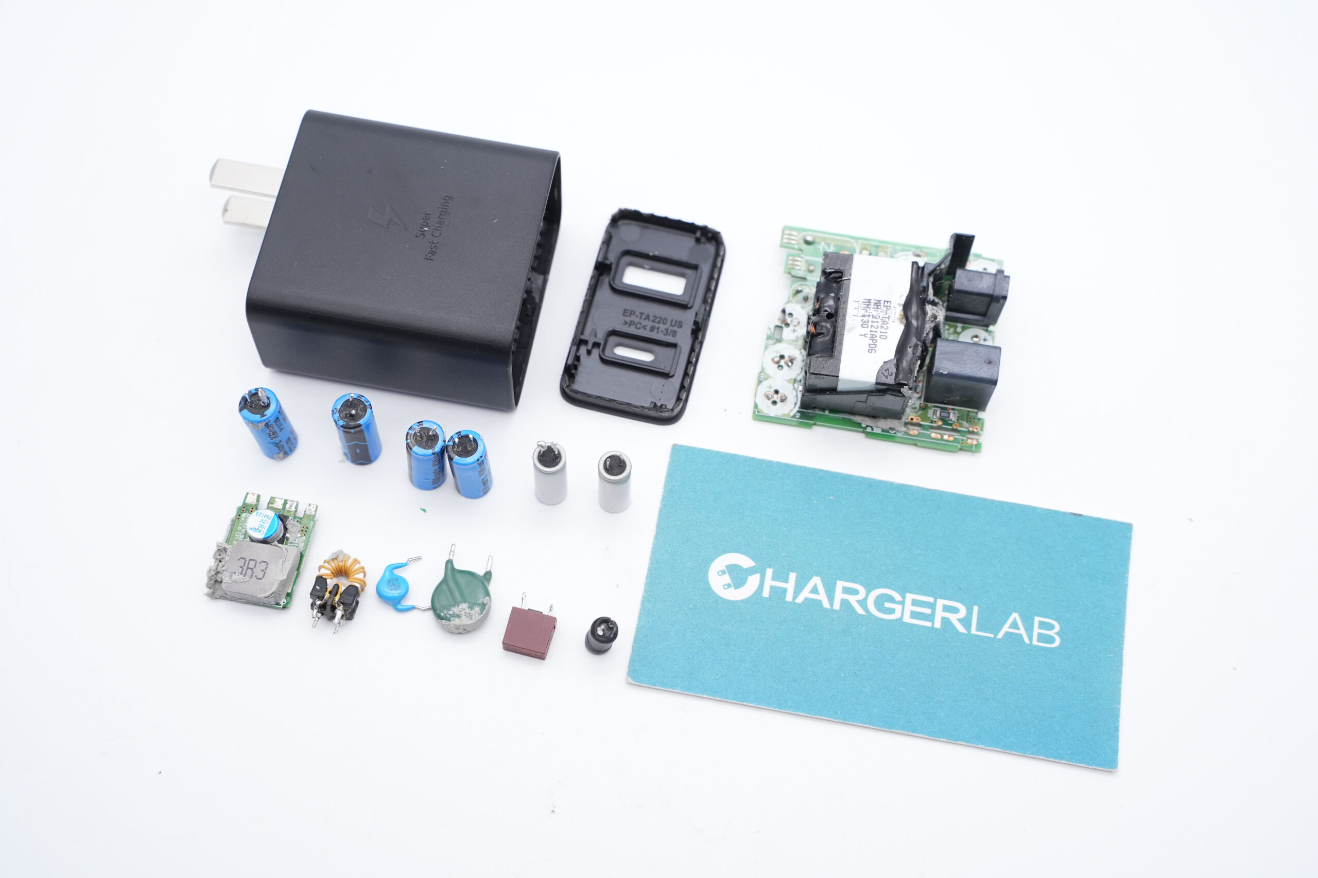
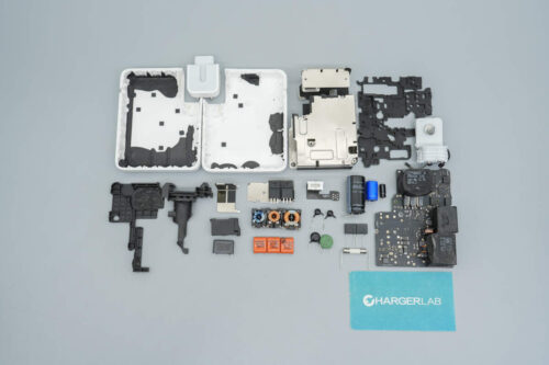
One last look at all the components of this Samsung 35W dual ports charger.
Summary of ChargerLAB
This Samsung 35W charger adopts black and fixed plug design. It also features 1A1C dual ports, with the USB-C port capable of delivering up to 35W of output power when used alone. When both the USB-C and USB-A ports are used simultaneously, the charger can support power distribution of 20W and 15W respectively, which satisfies the need for simultaneous charging of two devices while retaining excellent fast-charging compatibility. It's like the Samsung 65W trio charger we took apart before, but he has one less USB-C port, and the output power is also halved.
After taking it apart, we found two USB ports share the same switching power supply circuit, but are controlled by two different protocol chips, and USB-A port is controlled by a buck-boost circuit. If the Samsung 65W is out of your budget, you can consider this.
Related Articles:
1. Teardown of Samsung 35W 1A1C Dual Port Fast Charger (video)
2. Teardown of New Samsung 45W GaN Charger EP-T4510
3. Teardown of Samsung 25W USB-C Fast Charger (EP-TA800)

