Introduction
As we all know, Samsung has achieved great success in the phone industry, becoming one of the top smartphone manufacturers globally. And today, we got our hands on a Type C version of Samsung 15W charger, which is mainly used in most countries in the EU and India. So let's go ahead and take it apart to see its internal comonents and structure.
Product Appearance
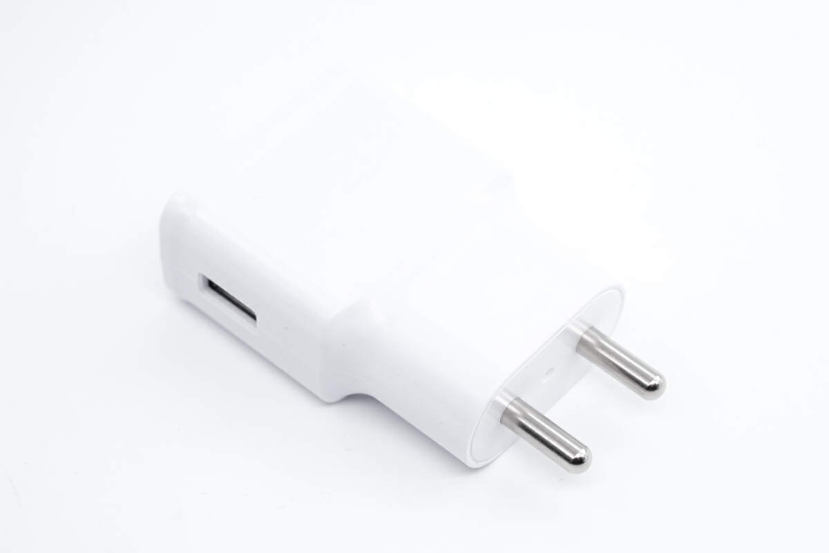
The charger features a classic two-part design, with a sleek matte finish and rounded edges.
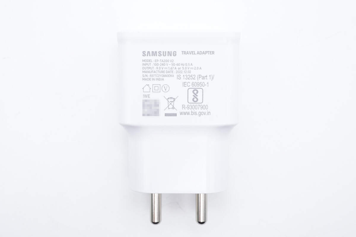
On the back, you can find the model of the charger - EP-TA200 V2 - alongside its specs info, including an input voltage range of 100-240V~50/60Hz 0.5A and an output of either 9V1.67A or 5V2A.
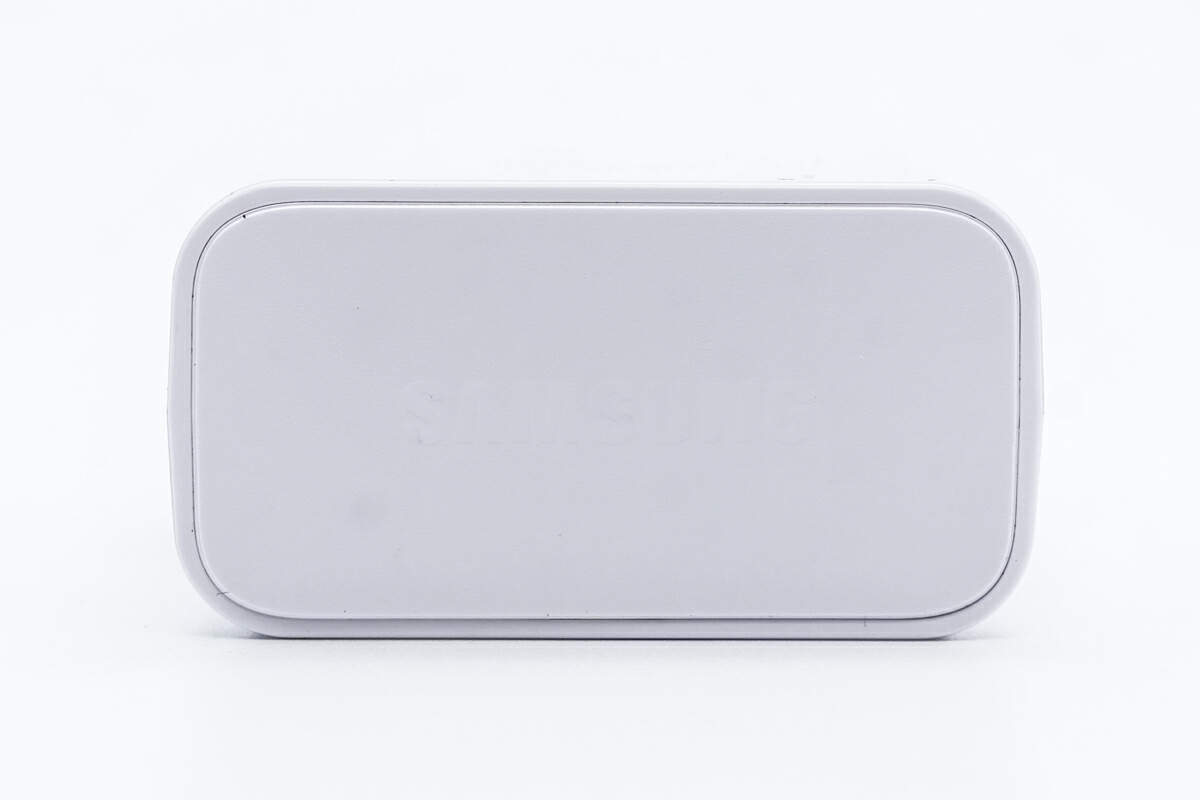
The SAMSUNG brand is subtly embossed on the top, adding to its overall aesthetic appeal.
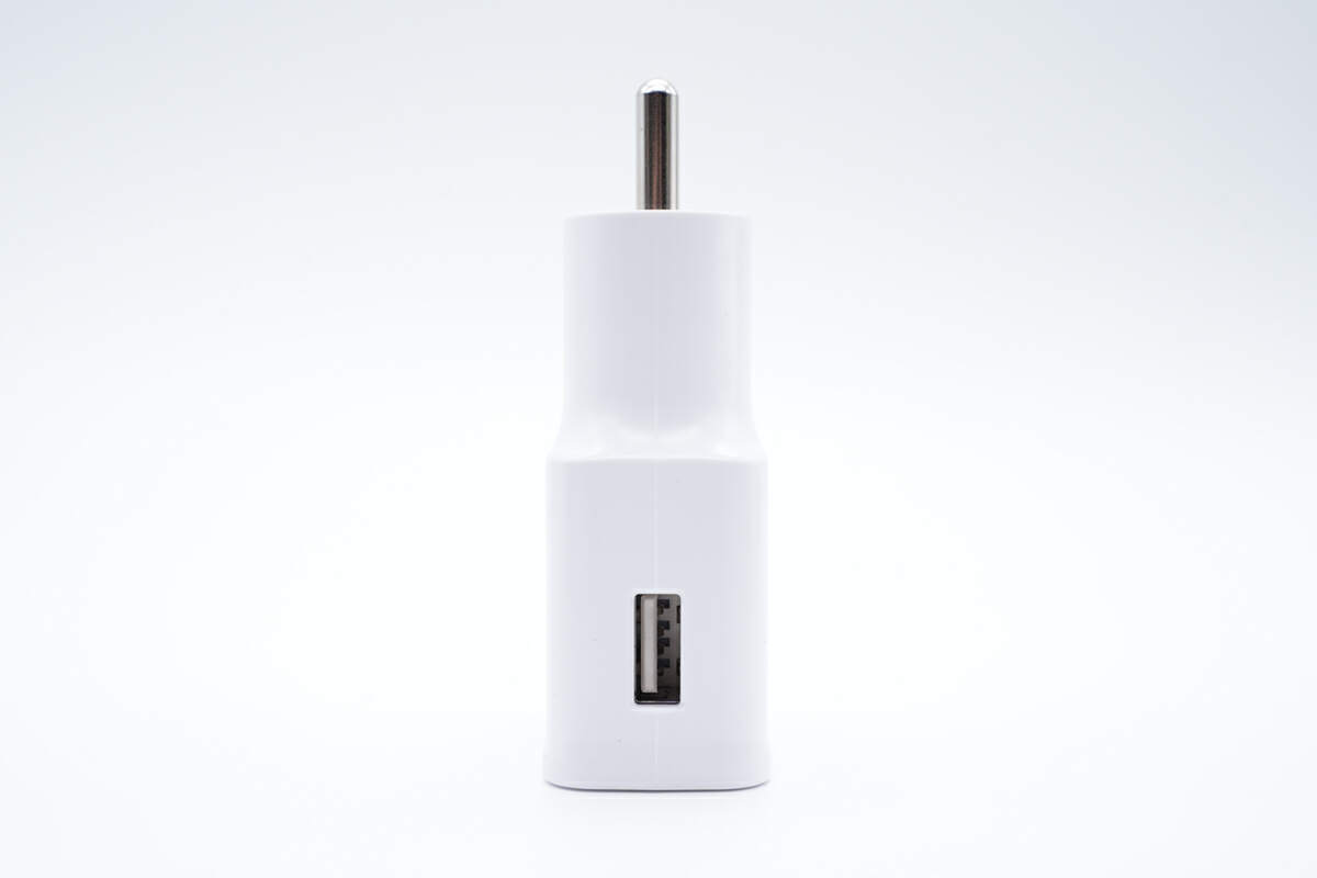
Additionally, the USB-A output port is conveniently located on the side of the charger for easy access.
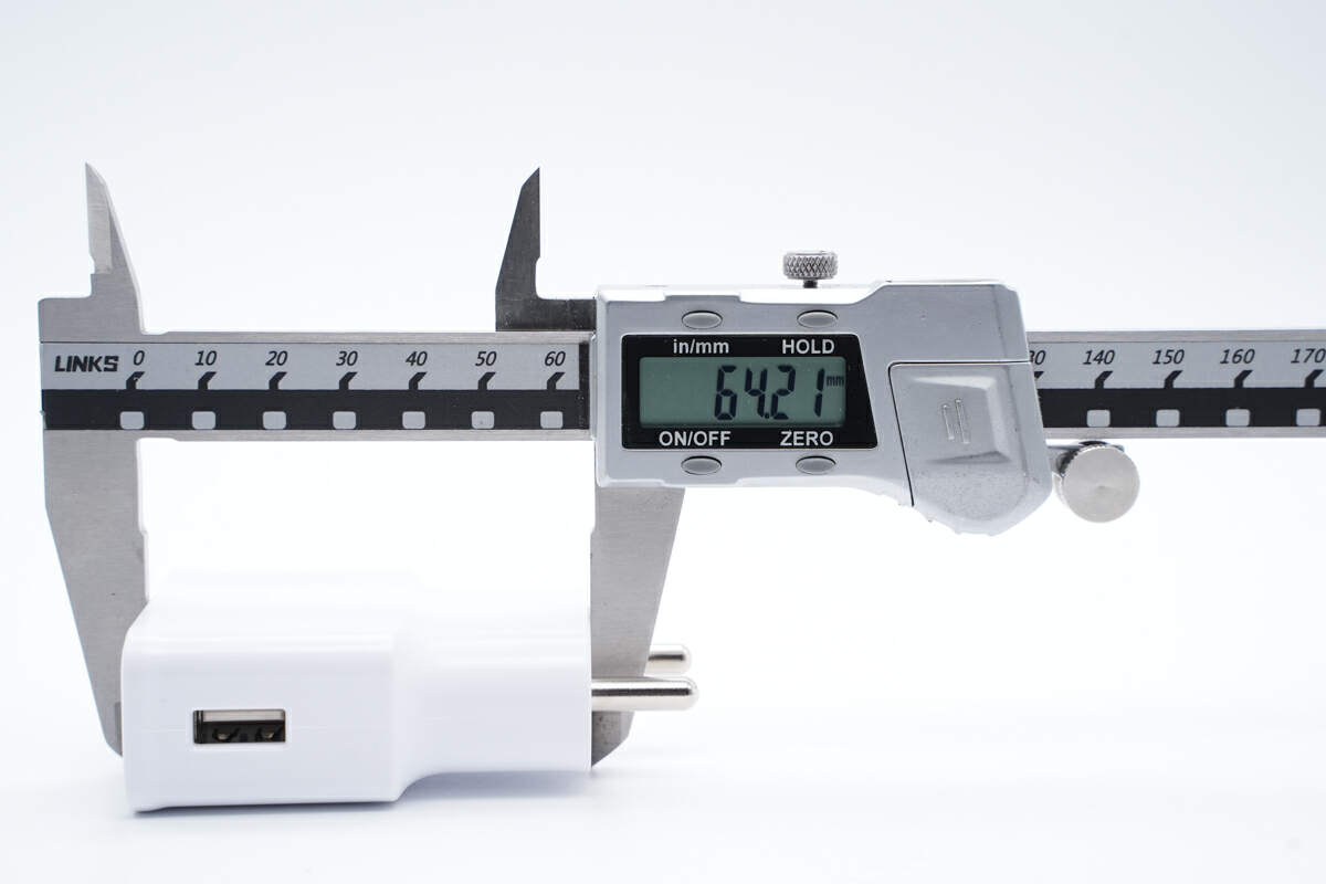
The length of the charger is about 64.2mm (2.53 inches).
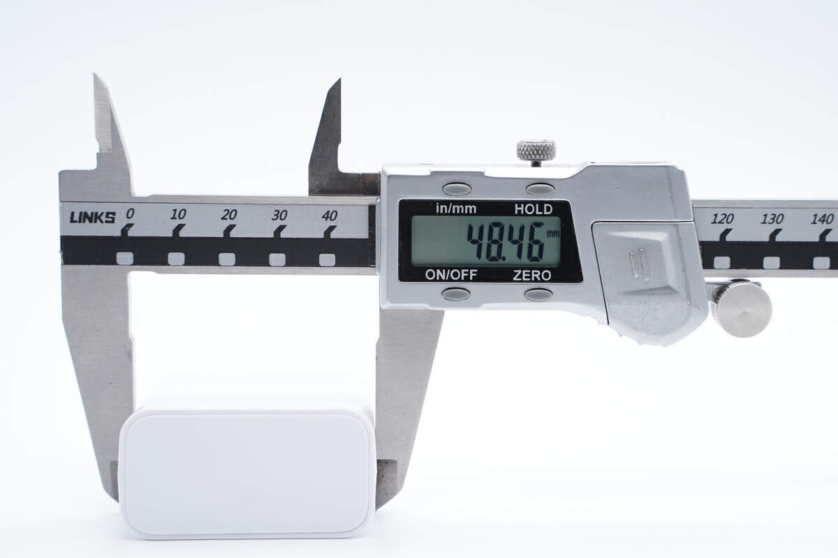
The width is about 48.5mm (1.91 inches).
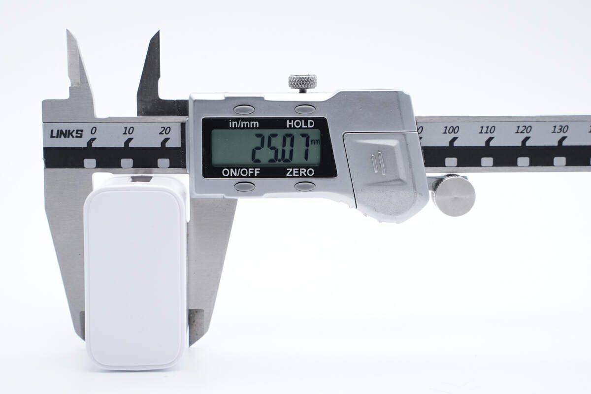
And the height is about 25.1mm (0.99 inches).
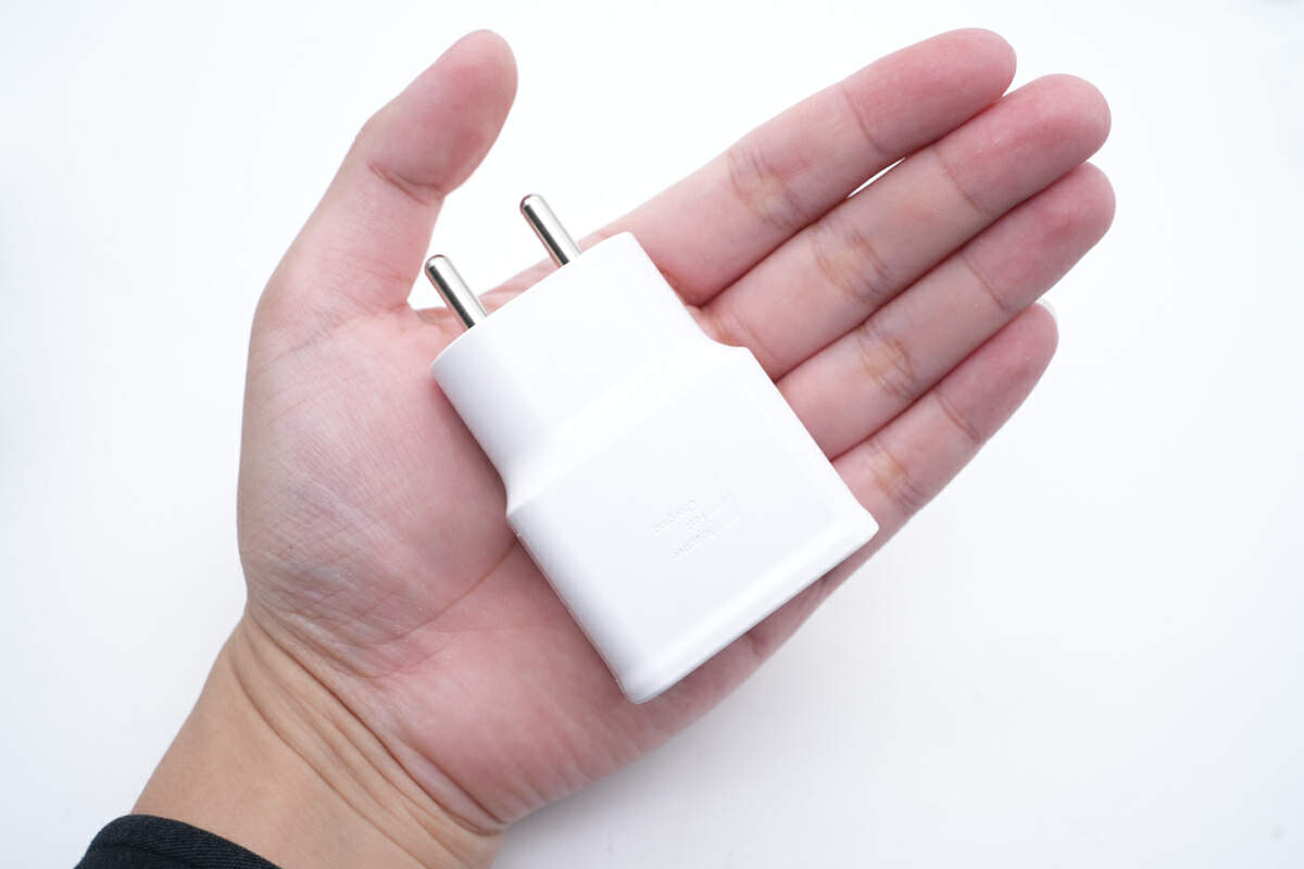
This is how it looks like on my hand.
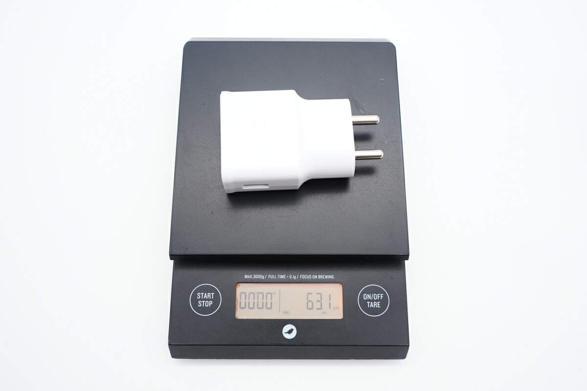
The weight is about 63 (2.22 oz).
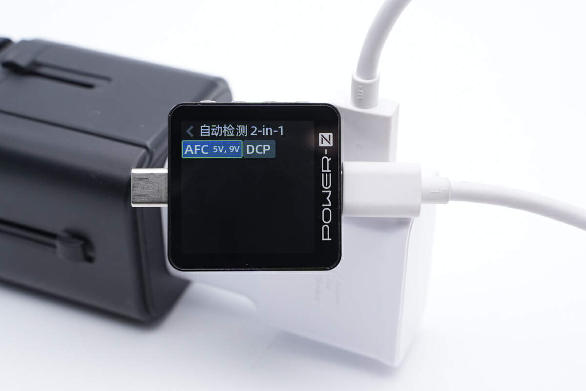
The ChargerLAB POWER-Z KM002C shows the charger supports Samsung AFC and DCP protocols.
Standby Power Consumption Test
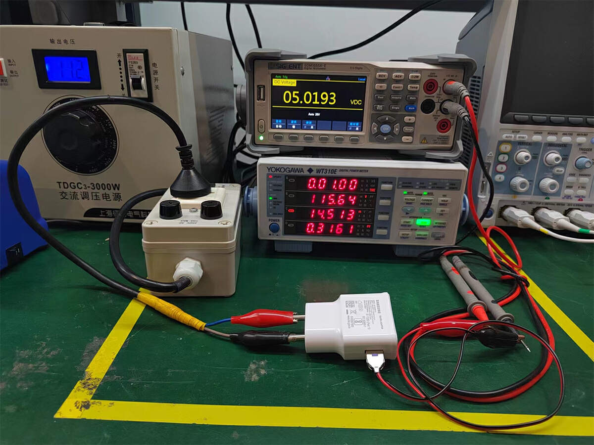
The first test conducted is the standby power consumption test with an AC input voltage of 115V. The standby power consumption for a 5V output is 14.51mW.
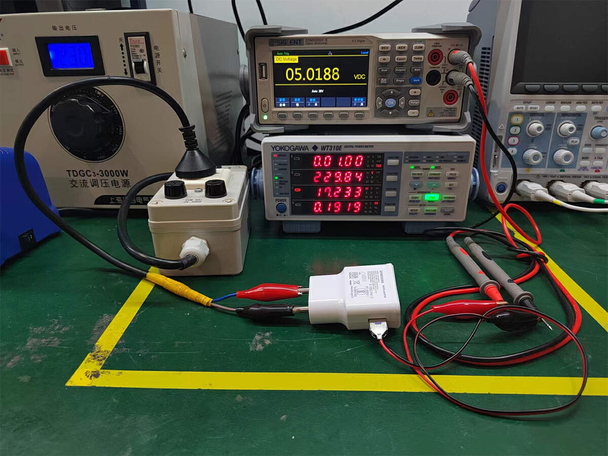
Under an AC input voltage of 230V, the standby power consumption for a 5V output is 17.23mW. This is far below the international standard of 75mW and is the first time a standby power consumption of under 20mW has been recorded for a charger, pretty impressive.
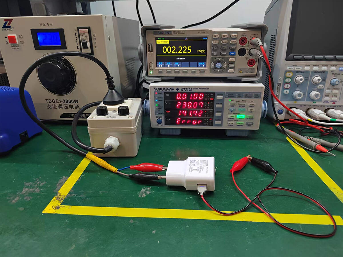
We then test the short-circuit power consumption under an AC input of 230V. The device displayed a power consumption of 141.42mW during short-circuiting, which is low enough to prevent heat generated by the port during short-circuiting.
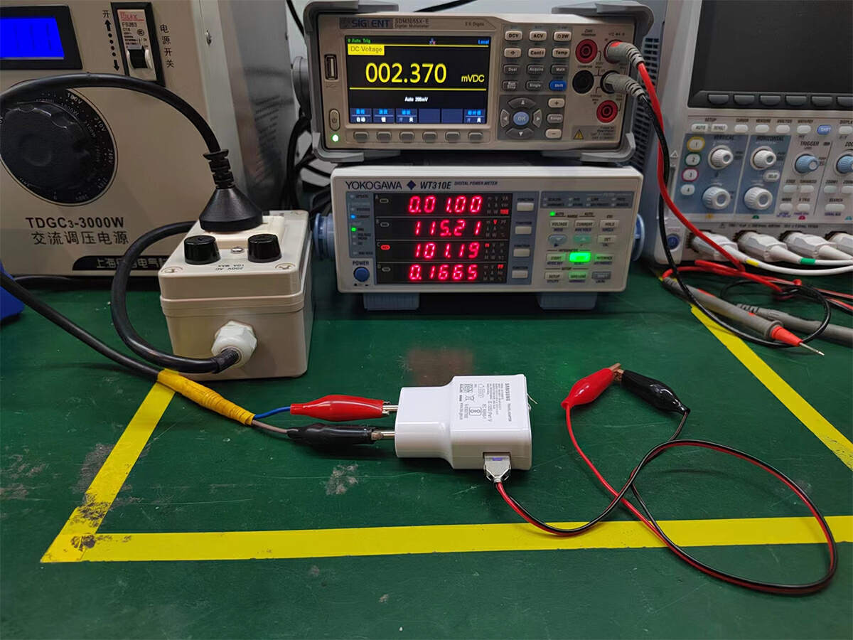
The output short-circuit power consumption under an AC input of 115V is 101mW.
Teardown
Next, take it apart to see its internal comonents and structure.
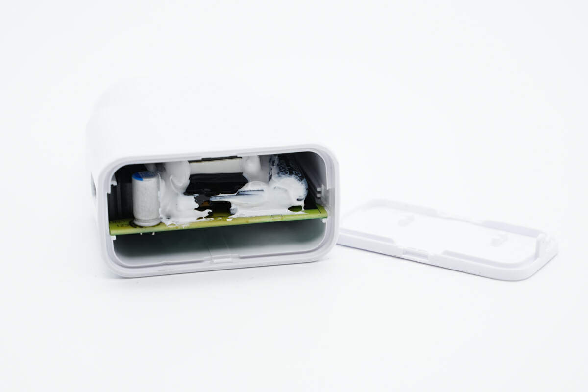
Firstly, pry open the top cover of the charger to reveal the internal PCBA module.
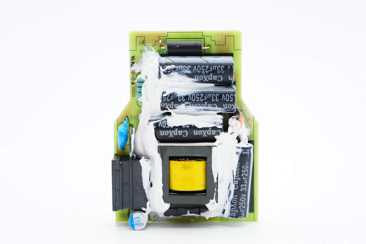
Remove the PCBA module. The electrolytic capacitor and transformer are fixed in place with white silicone adhesives, while the USB-A socket has an insulated shell.
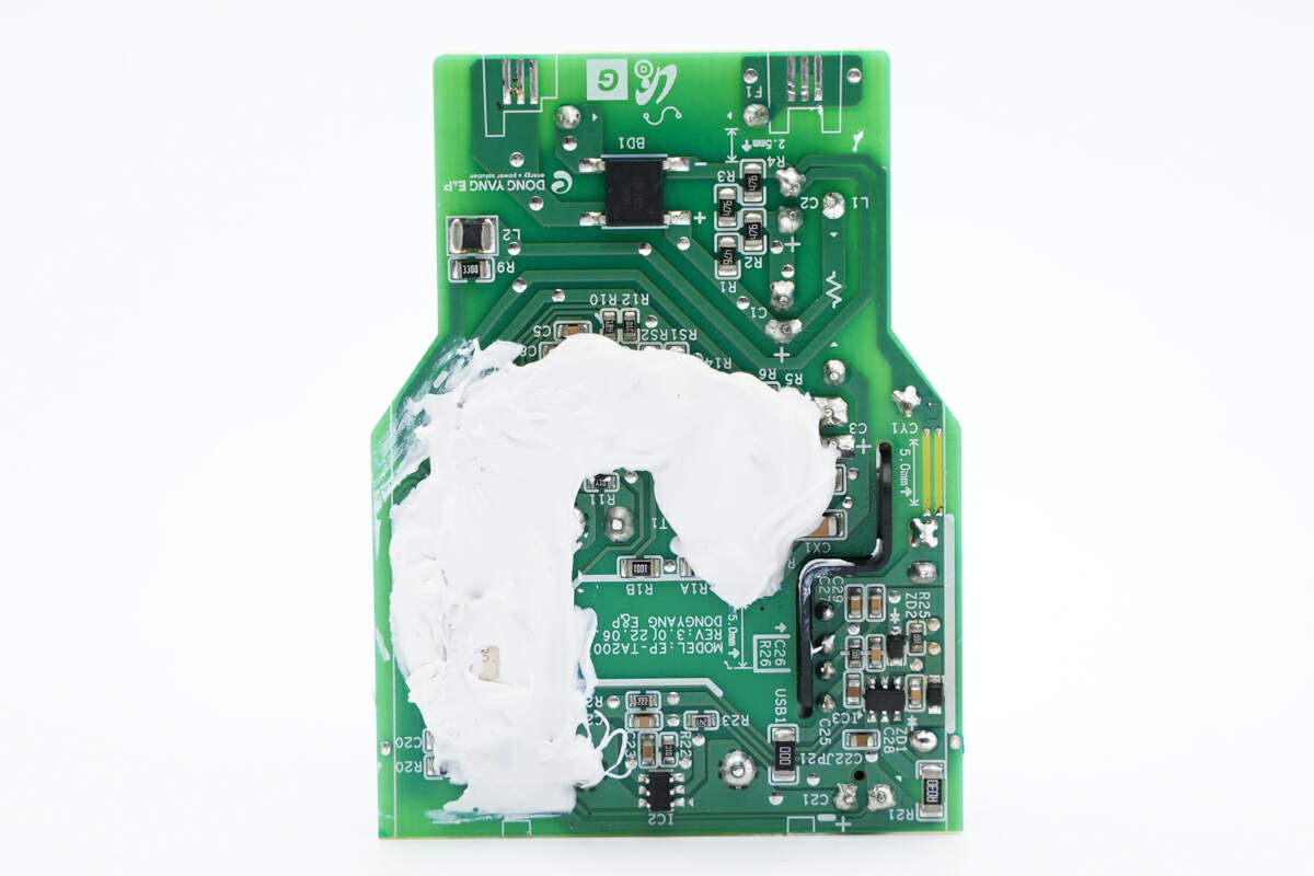
The back of the PCBA module has heating components that are also covered in silicone adhesives for heat dissipation, with power contact points located at the top of the module.
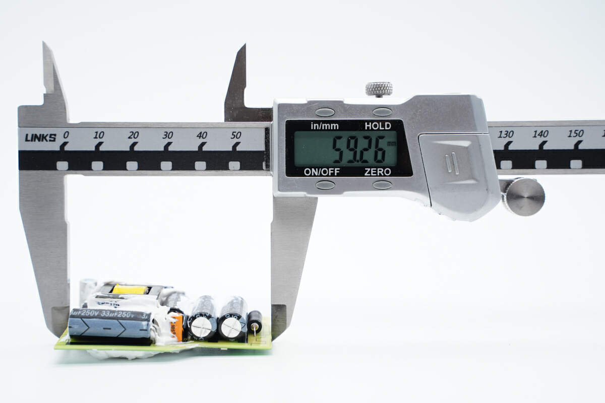
The length of the PCBA is about 59.3mm (2.33 inches).
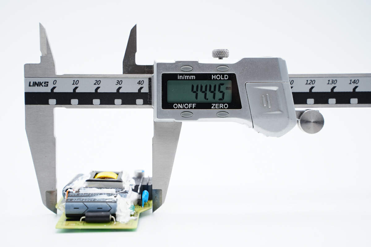
The width is about 44.5mm (1.75 inches).
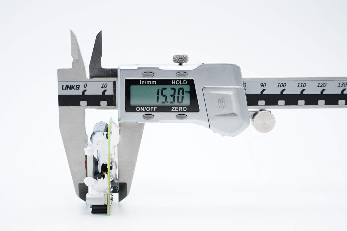
And the height is 15.3mm (0.60 inches).
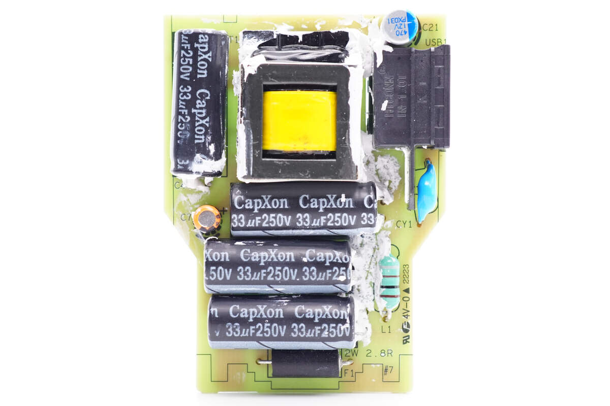
The fuse resistor, high-voltage filter capacitor, differential mode inductor, transformer and blue Y capacitor are on the front of the PCBA module.
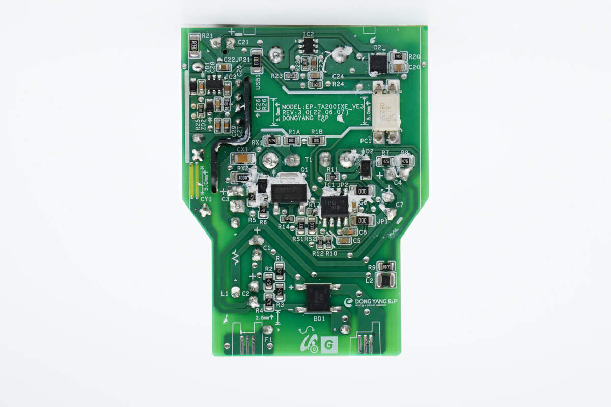
And after cleaning up all the adhesives on the back, we can see the bridge rectifier, master control chip, primary MOSFET, feedback optocoupler, synchronous rectifier controller, and protocol chip on it.
The PCB model of this Samsung charger is EP-TA200IXE. ChargerLAB found that the switching power supply and protocol chip of this charger are both sourced from Hyasic Semi, which provides a complete set of solutions. The output voltage of the charger is adjusted by the protocol chip through optocoupler control, achieving 5V and 9V output voltages.
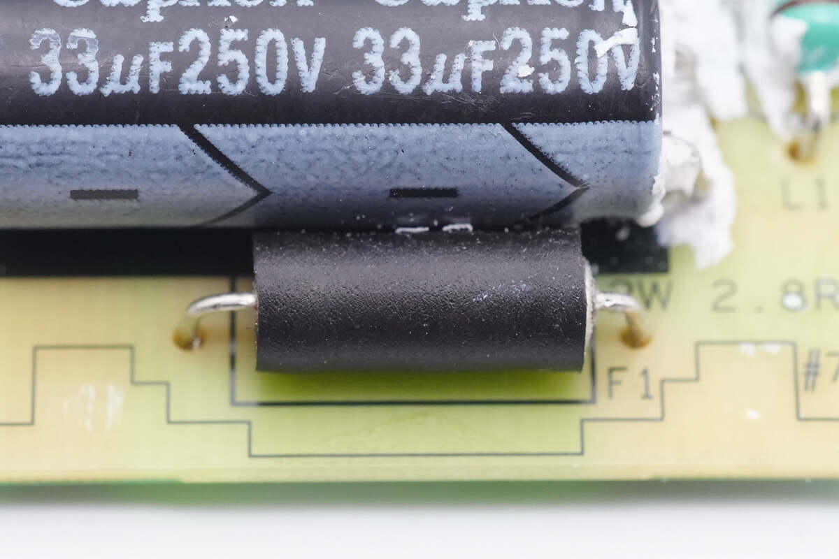
To protect against input overcurrent and suppress surge currents, a 2W 2.8R fuse resistor has been implemented.
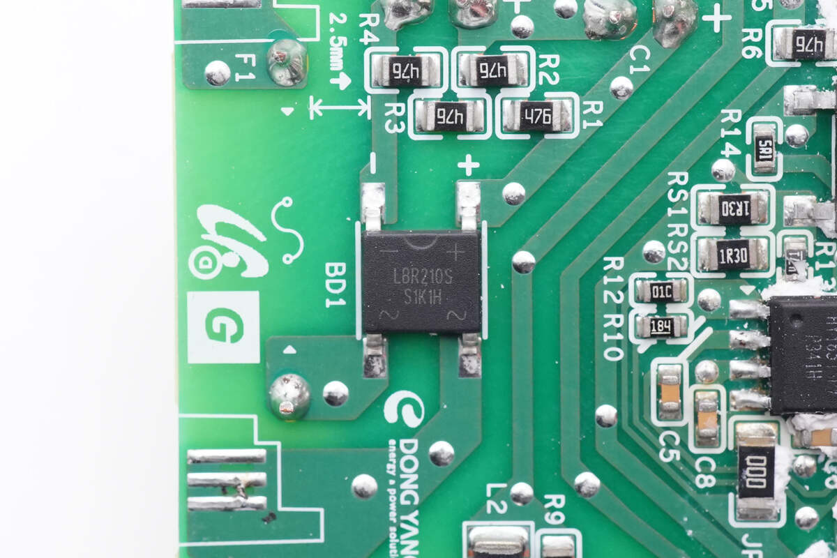
The input-side of the device implements an LBR210S fast recovery bridge rectifier with a specification of 1000V 2A.
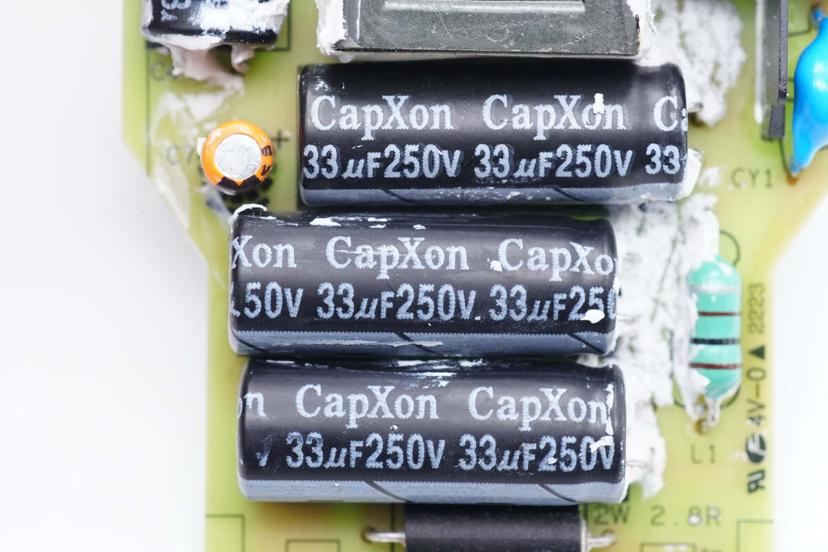
These high-voltage filter capacitors originate from CapXon. 33μF 250V.
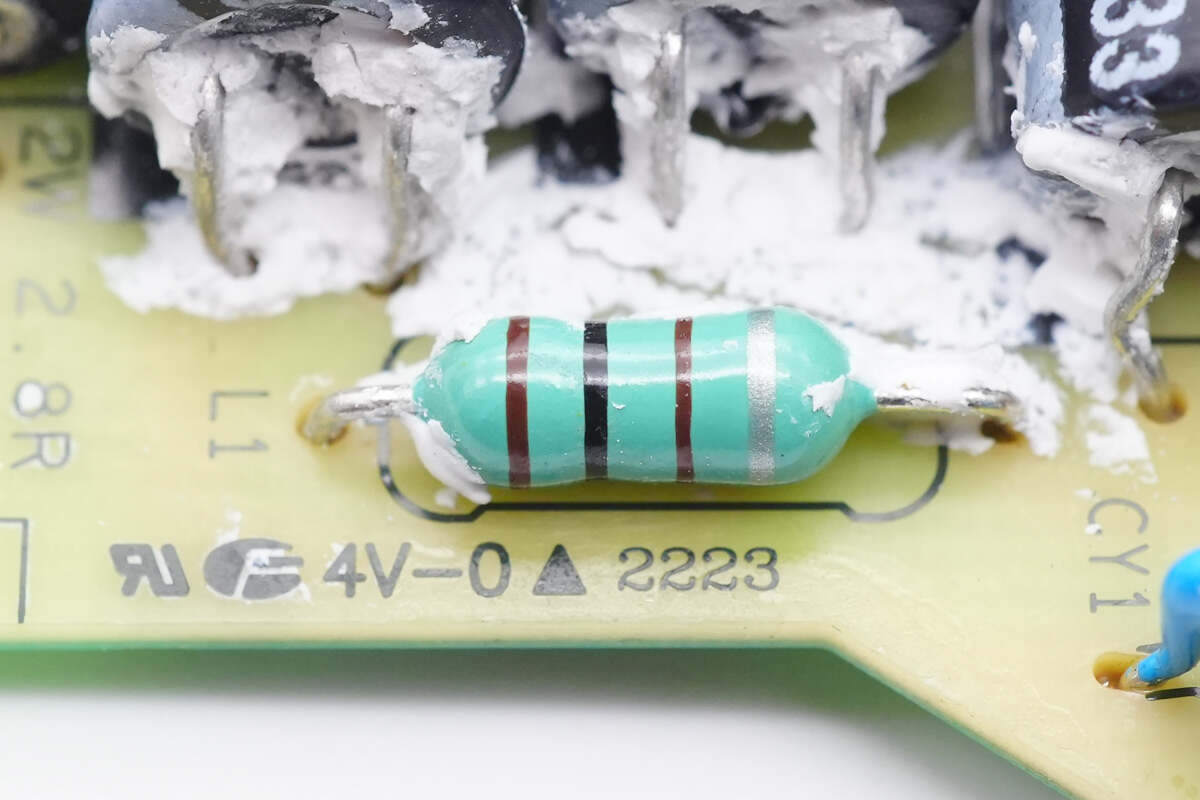
A small color code differential inductor is next to them.
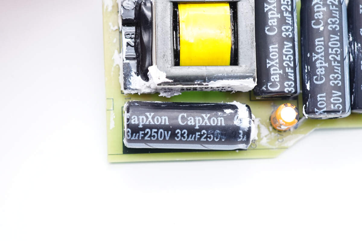
The four filter capacitors operate in pairs, connected in series then parallel, resulting in an equivalent total input capacitance of 33μF/500V. It is worth noting that the filter capacitor's withstand voltage in this charger is 250V. By connecting two capacitors in series, the withstand voltage can reach up to 500V, making it suitable for use in an ultra-wide input voltage ranging from 90Vac to 300Vac.
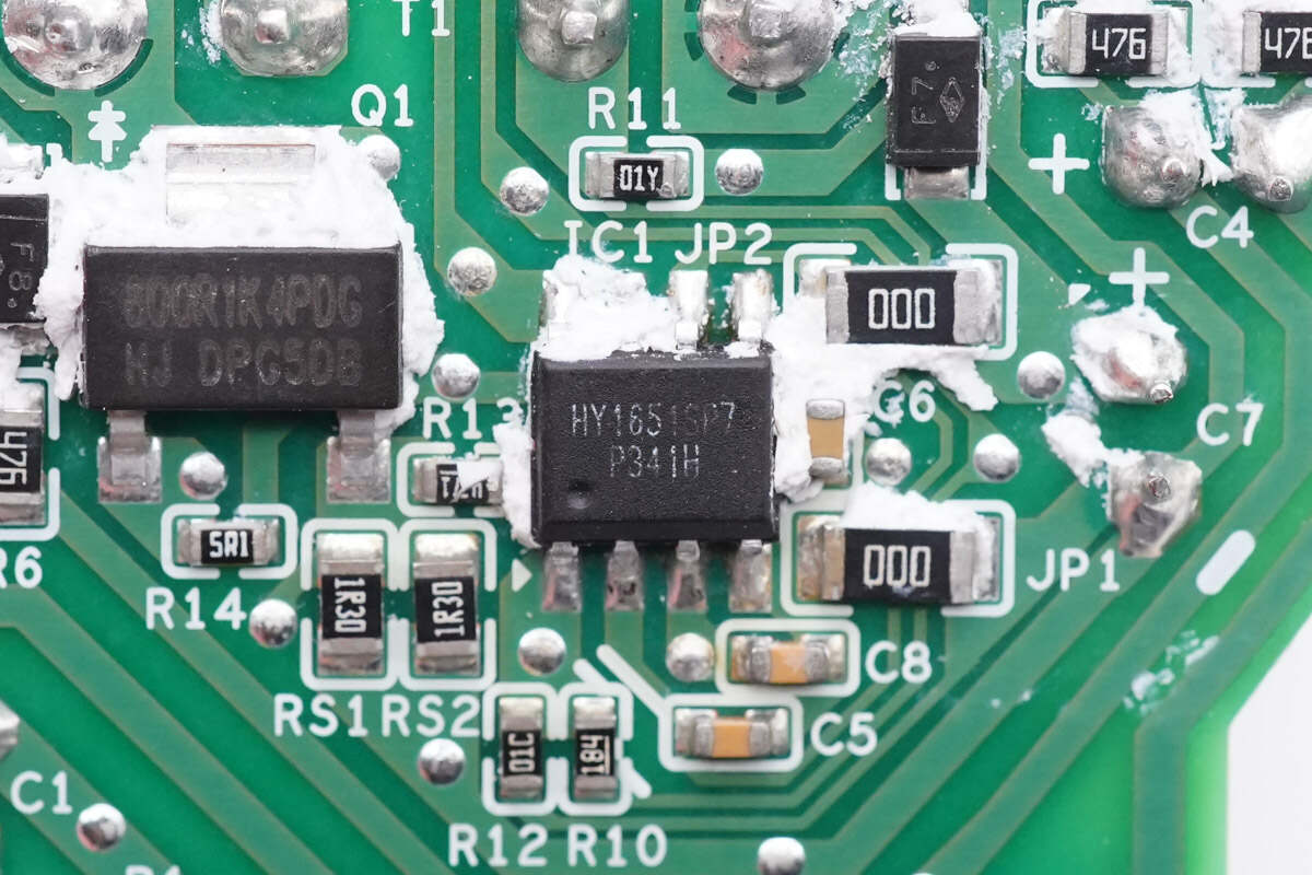
The master control chip is from Hyasic Semi, model HY1651S, which is an intelligent digital multi-mode flyback controller with ultra-low standby power consumption. The chip integrates high-voltage startup, uses peak current mode control, supports frequency dithering to improve EMI performance. And it can also adaptive the MOSFET gate driver to balance switching loss and EMI, and has a built-in 12V gate drive voltage clamp to support the application scenario of ultra-low standby power consumption below 20mW.
The chip also has built-in output overvoltage and undervoltage protection, transformer saturation protection, overload protection, overheat protection and sampling resistor protection, suitable for chargers and power adapters.
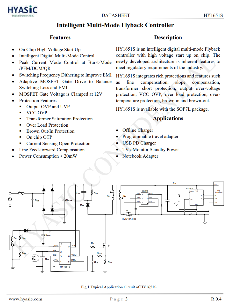
Here is all the information about Hyasic Semi HY1651S.
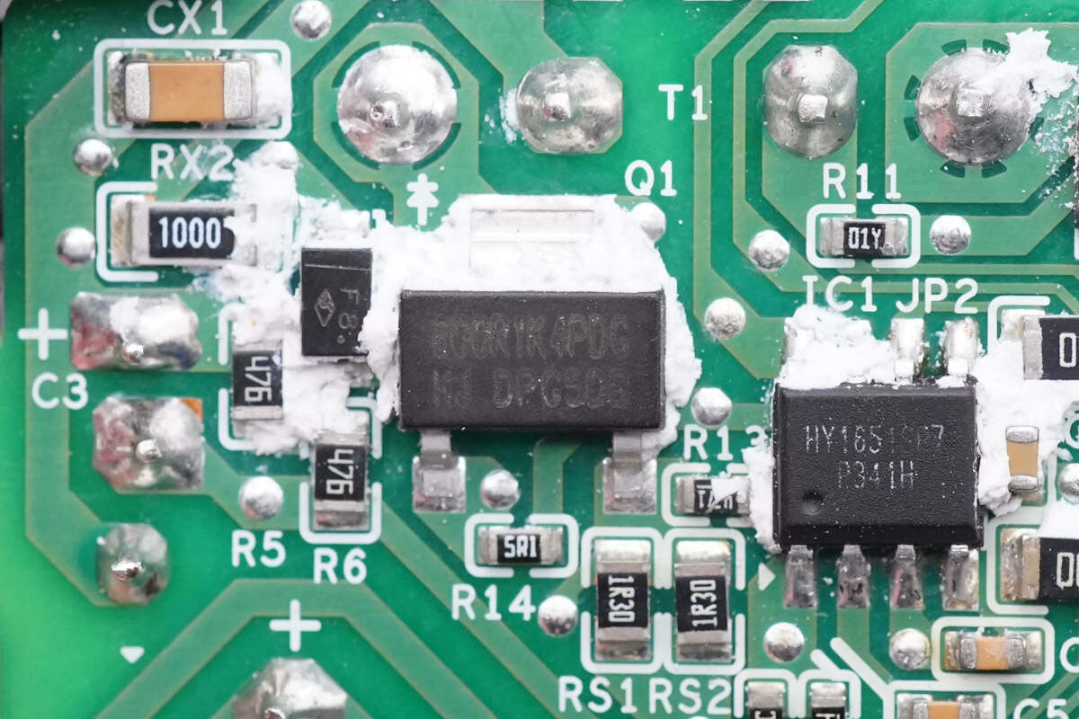
The MOSFET is marked with 800R1K4PDG, and adopts SOT223 package.
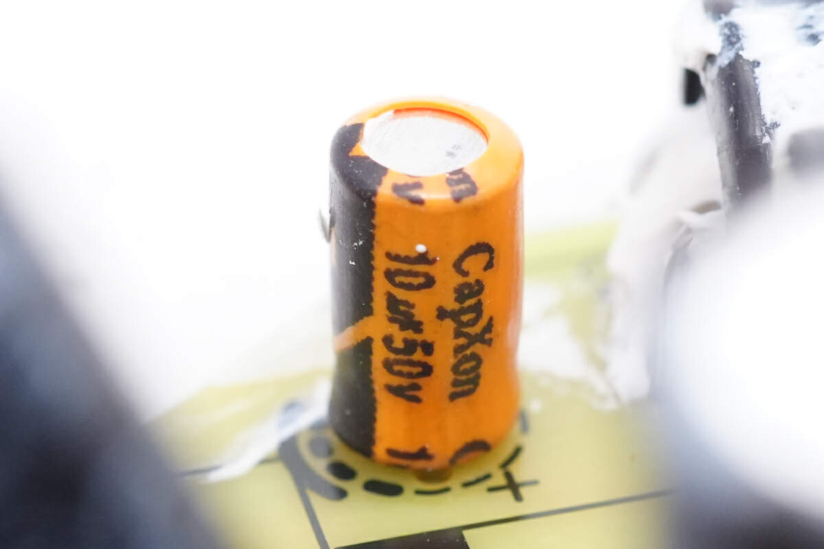
The filter capacitor that powers the master control chip is also from CapXon. 10μF 50V.
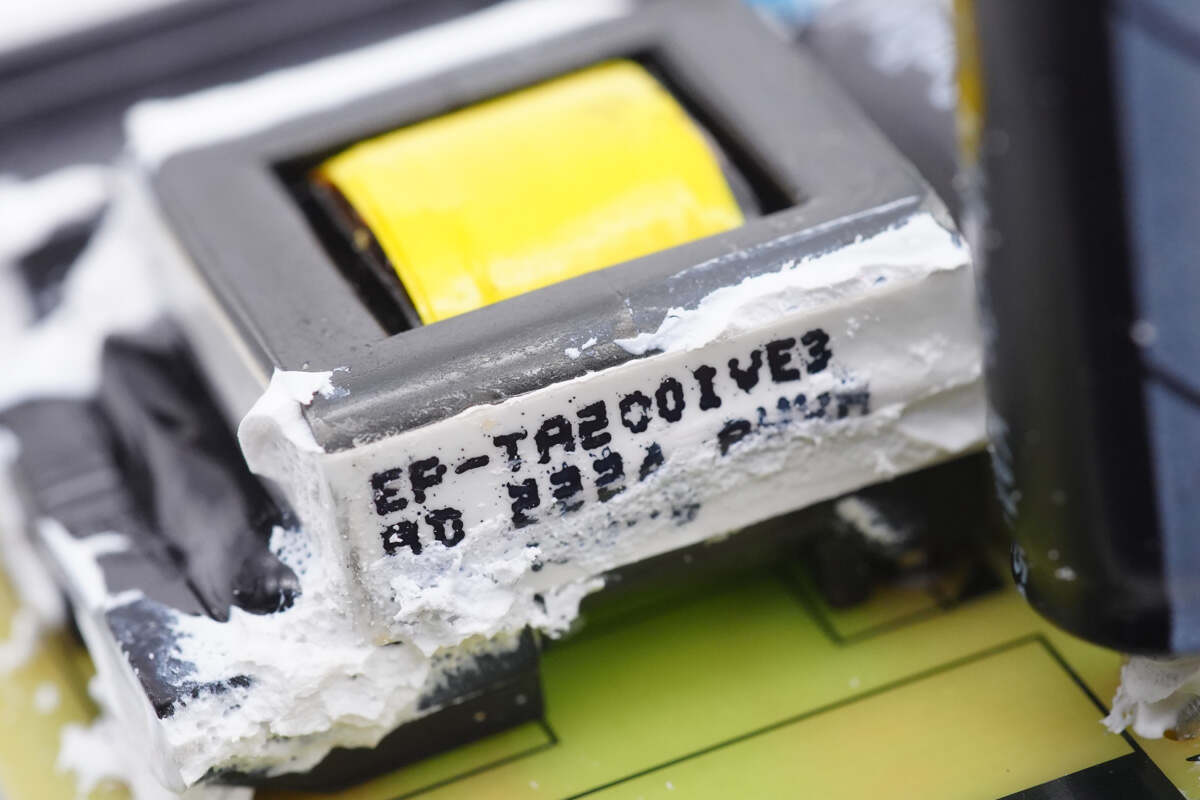
The model TA200 is marked on the side of the transformer's ferrite core.
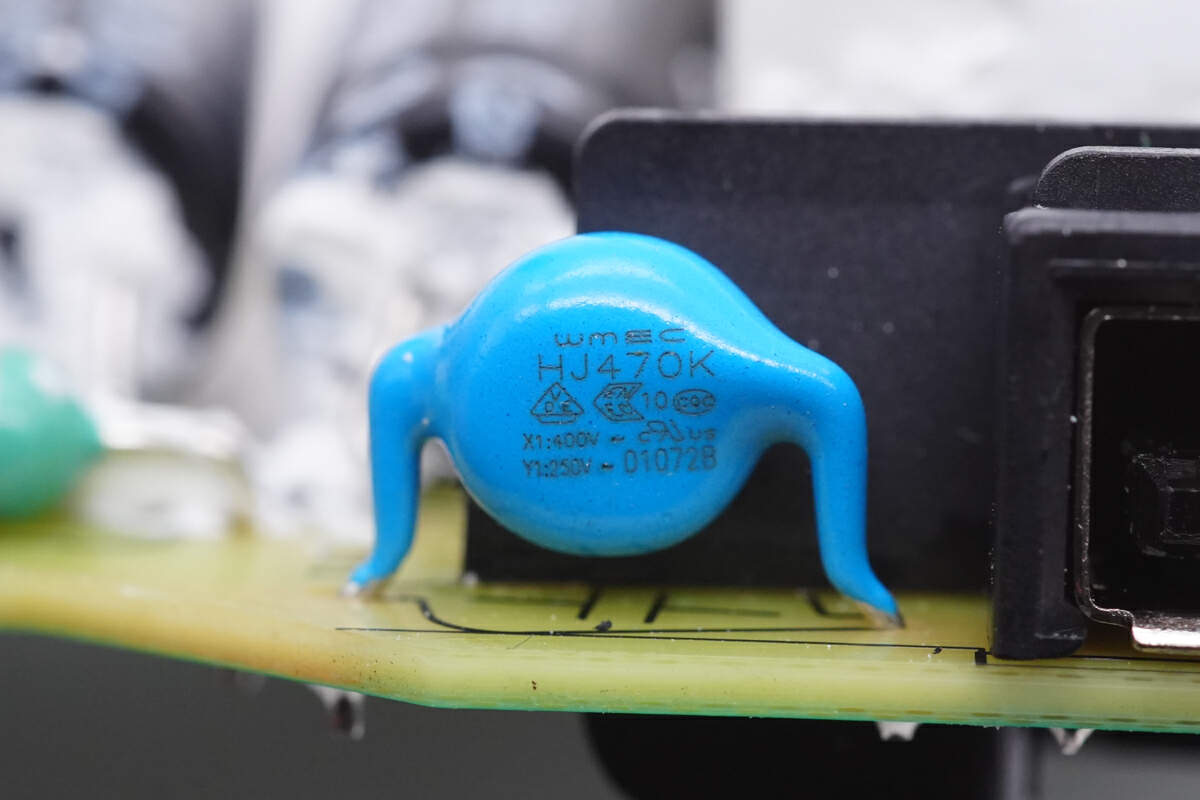
And this blue Y capacitor is from WMEC.
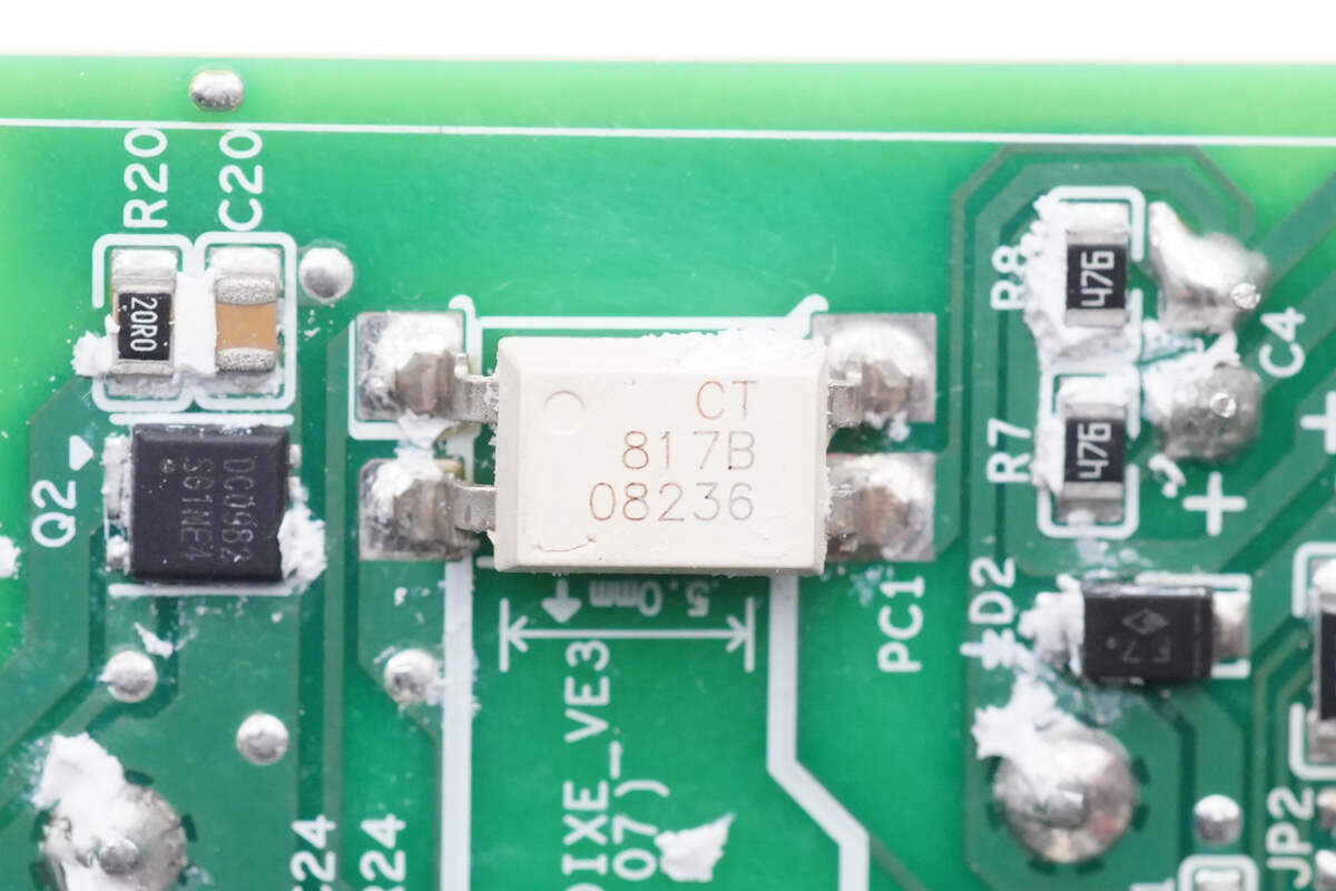
The CT817B optocoupler is used for output voltage feedback regulation.
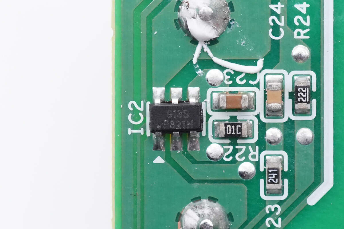
The Hyasic Semi HY913 is a smart digital control multi-mode synchronous rectifier controller, suitable for DCM/QR/CCM operation mode. The chip has a built-in charge pump that can boost the supply voltage to ensure complete conduction of the synchronous rectifier MOSFET, resulting in higher efficiency at low voltage output. It also supports the pre-turning off scheme, speeding up turn off transition, has a 10ns shutdown delay, and supports CCM working mode. It also add green mode to disable gate drive to improve the consumption at no load condition.
HY913 has a built-in Integration function, which can prevent synchronous rectifier MOSFET from turning on by mistake. The chip supports a power supply range of 3~25V, which meets the PPS power supply range. The chip also has built-in primary and secondary MOSFET simultaneous conduction protection. The high voltage drain sensing is up to 150V.
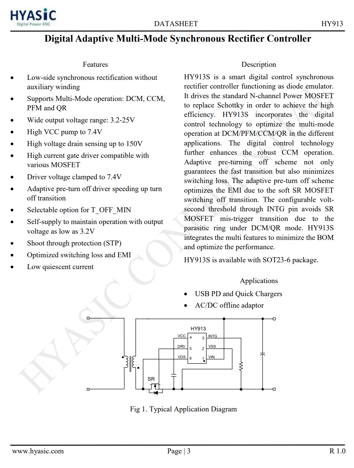
Here is all the information about Hyasic Semi HY913.
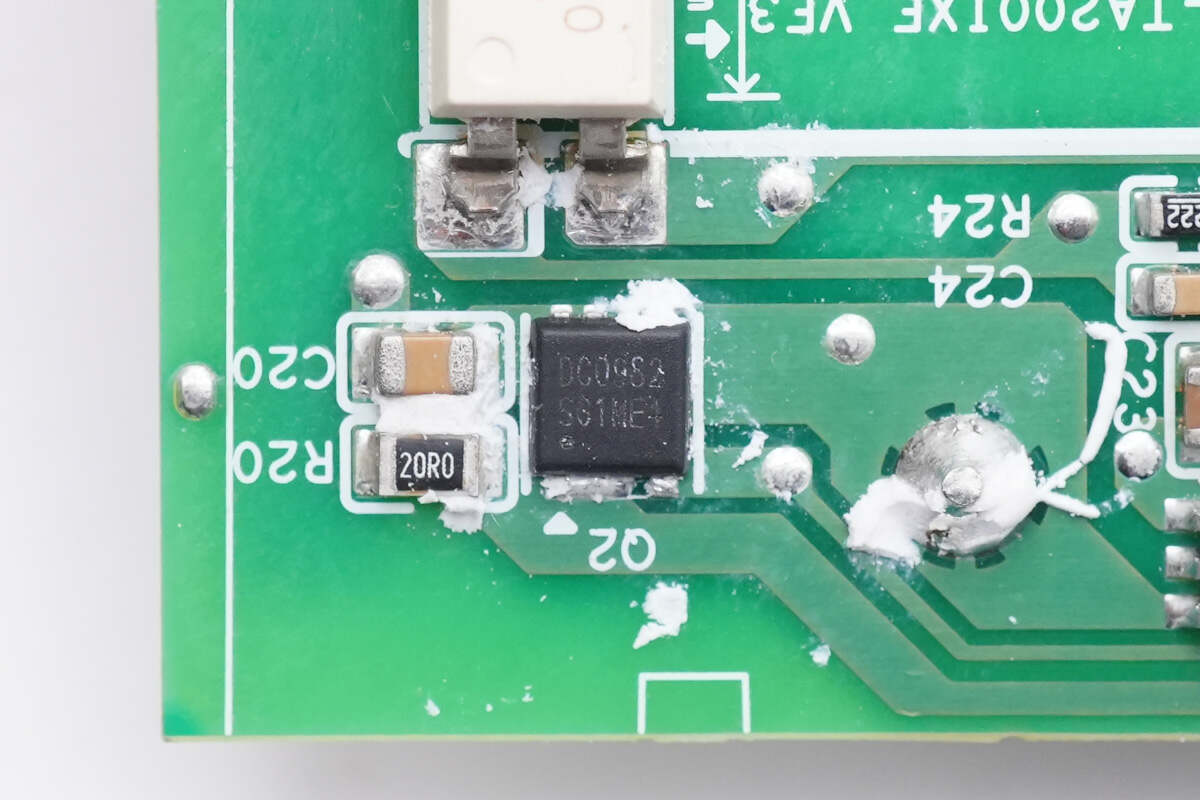
The synchronous rectifier MOSFET marked with DC0982 is controlled by that HY913.
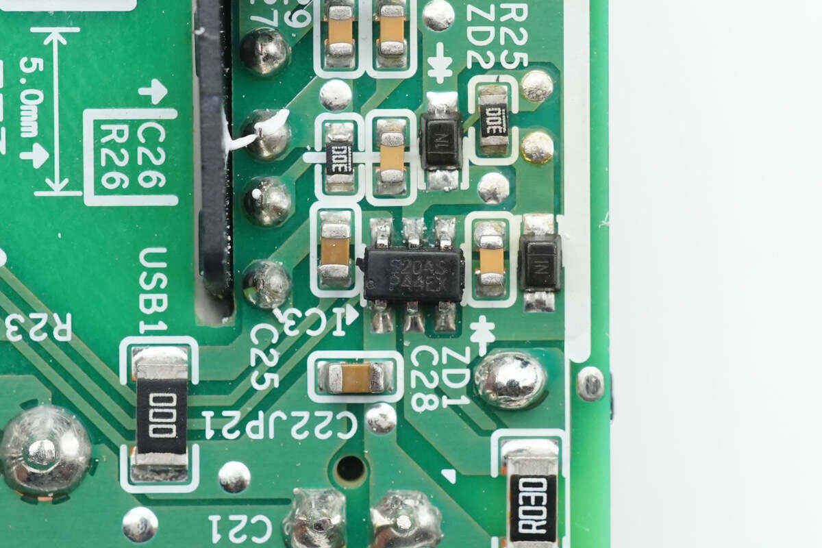
The Hyasic Semi HY5204S is a controller that supports Samsung AFC protocol. It supports two output power of 5V2A and 9V1.67A. The chip integrates a current sense amplifier and an external sampling resistor is used for output overcurrent protection. The chip supports constant voltage and constant current control, and integrates loop compensation and VBUS discharge, integrates cable drop compensation, supports output overvoltage, undervoltage protection, supports data pin overvoltage protection and micro-short circuit protection, and integrates overheating protection.
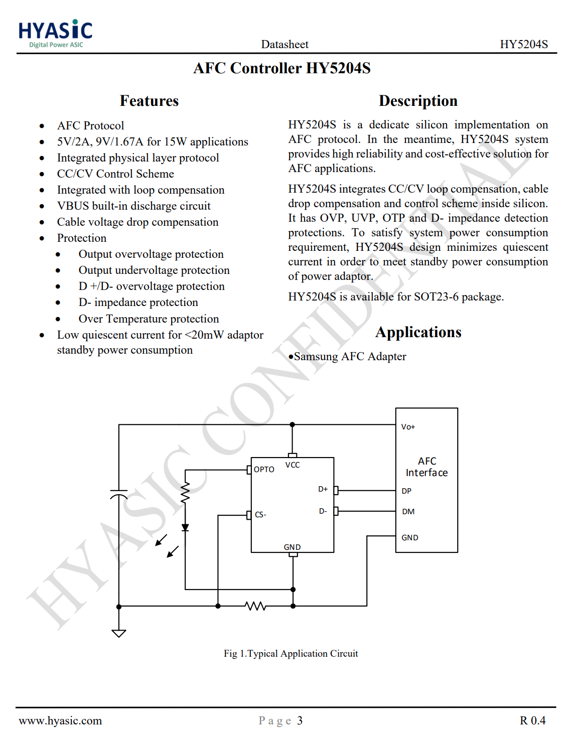
Here is all the information about Hyasic Semi HY5204S.
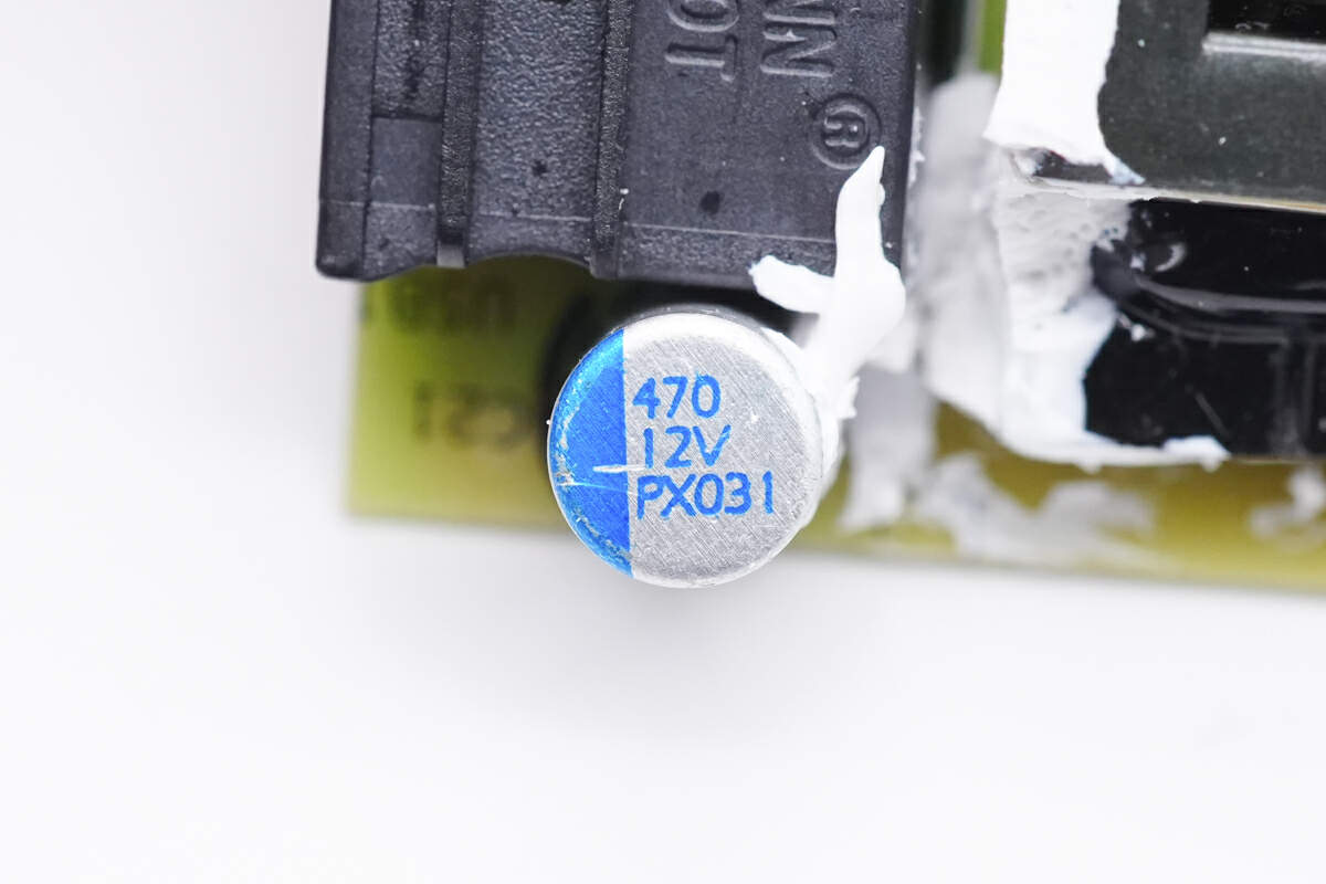
The blue solid capacitor for output filtering is from CapXon PX series. 470μF 12V.
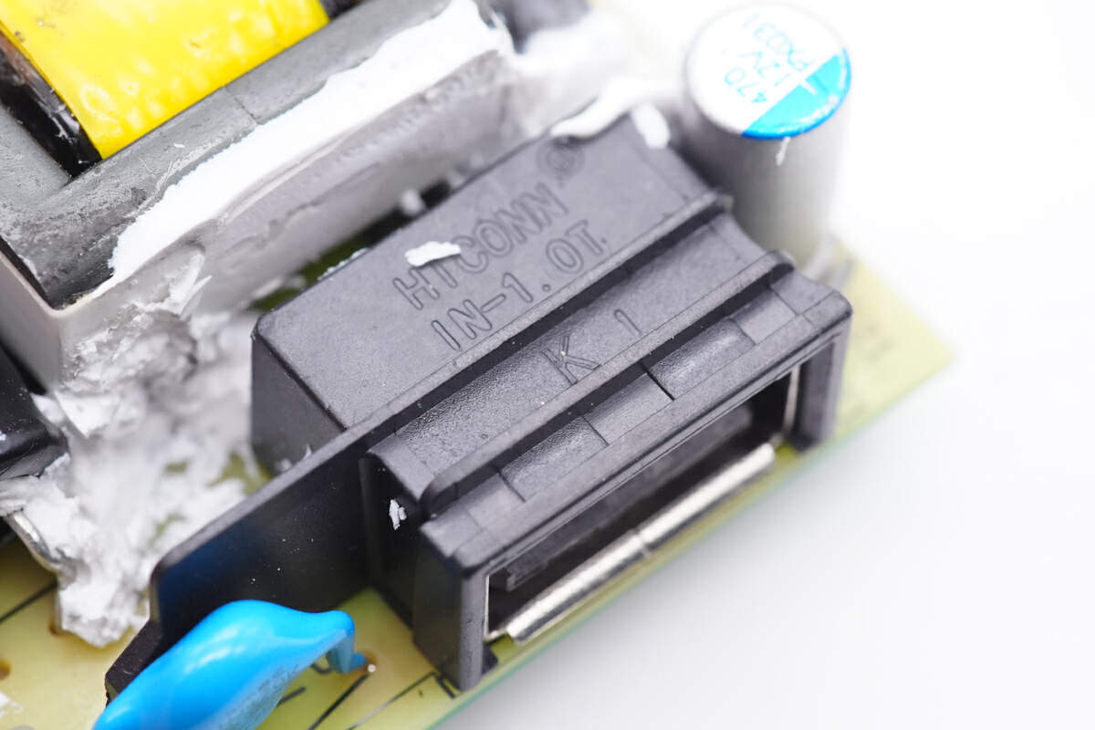
The USB socket is insulated by a plastic shell.
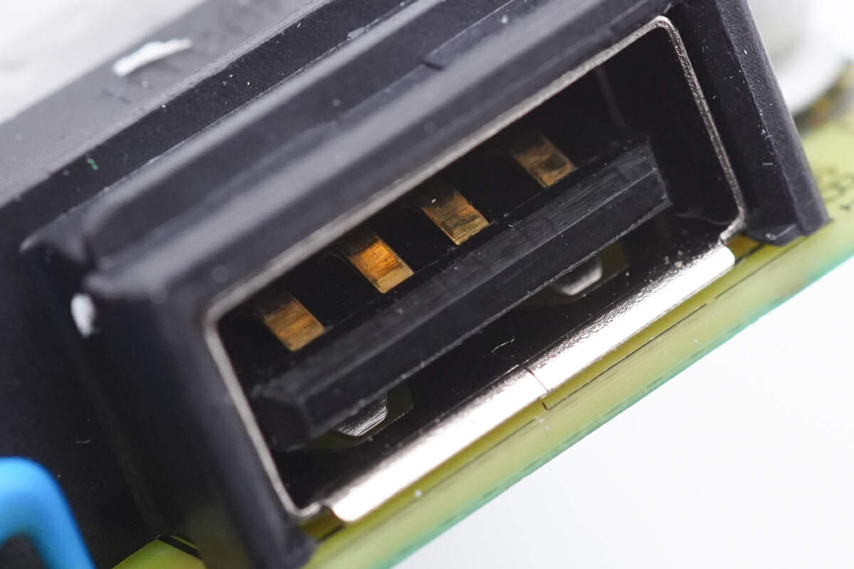
The plastic sheet inside the USB socket is black.
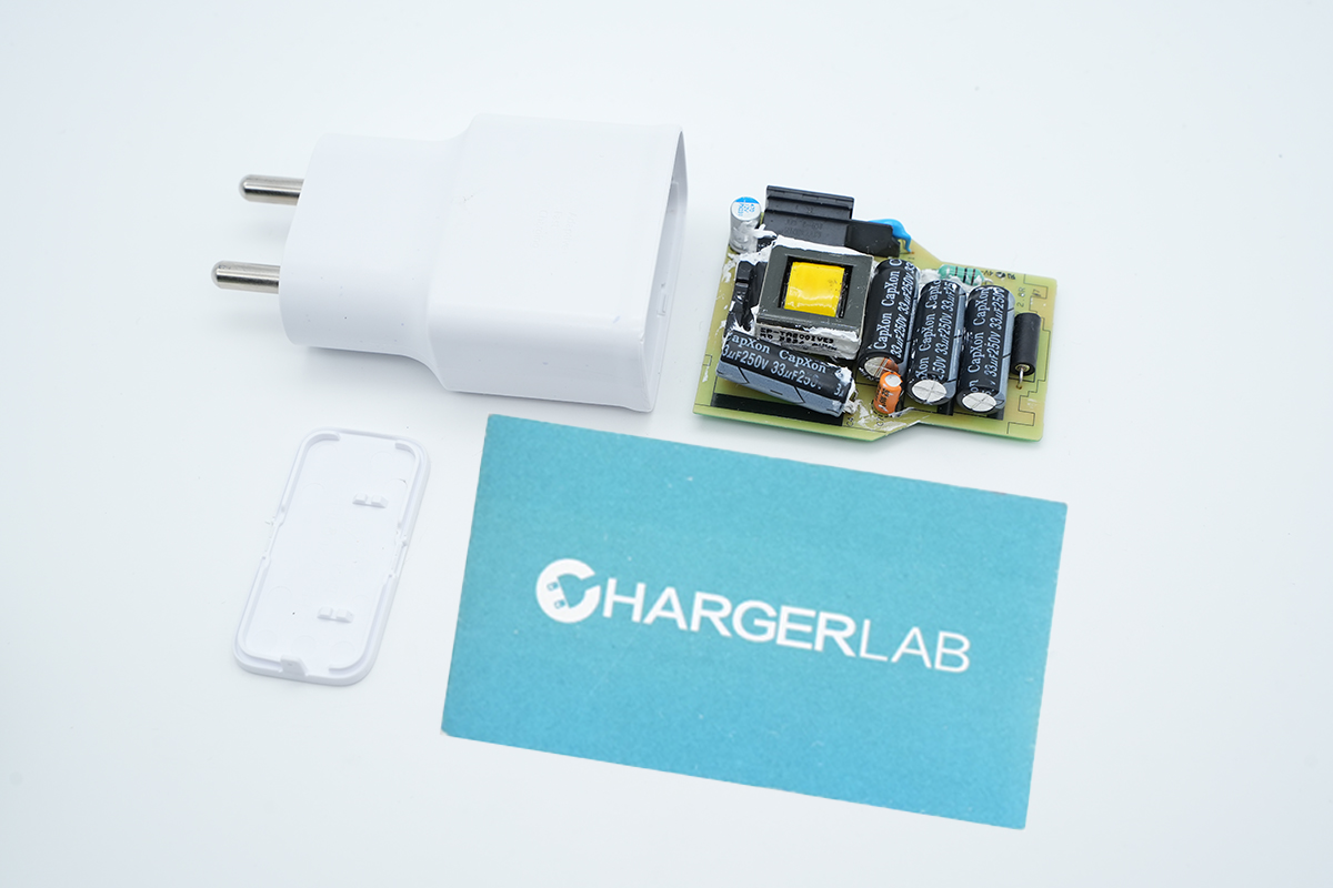
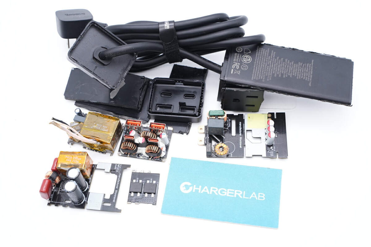
One last look at all the components of this Samsung 15W USB-A charger.
Summary of ChargerLAB
This Samsung 15W USB-A charger only supports the AFC fast charging protocol and has two output voltages, 5V and 9V. Designed with a classic appearance, Samsung users should find it very familiar. This charger is equipped with a round plug that is mainly used in most countries in the EU and India and supports an ultra-wide working voltage range of 90Vac~300Vac, which can meet different power supply voltages around the world.
ChargerLAB discovered that Samsung has implemented Hyasic Semi HY1651S plus HY913S fast charging switch power supply solution, along with an HY5204S protocol chip. With standby power consumption as low as 18mW, this charger is highly energy-efficient. All internal capacitors are sourced from CapXon, and the internal components are fixed in place with silicone adhesives, ensuring good heat dissipation. Moreover, the internal materials and workmanship demonstrate high-quality craftsmanship throughout.
Related Articles:
1. Teardown of Samsung 25W USB-C Fast Charger (EP-TA800)
2. Teardown of Samsung 45W USB-C Fast Charging Wall Charger
3. Teardown of Samsung 100W USB-C Cable (For New 45W Charger)

