Introduction
As we all know, Nintendo Switch is one of the best-selling game consoles all around the world. Last year, Nintendo upgraded the traditional non-laminated LCD screen to a fully-laminated OLED screen, bringing more vivid graphics, brighter colors and stronger contrast to enhance the visual experience of the game. At the same time, the internal storage was upgraded from 32G to 64G.
Compared with the old one, the dock of the OLED version uses a gigabit ethernet port instead of the USB3.0 port, which makes the network connection more stable. Now, let's take a look at what's inside the dock.
Product Appearance

The Nintendo Switch OLED charging dock uses a black plastic shell, in addition to the slot in the middle of the dock, there are logo, non-slip pads, etc.

Compared with the old version, the logo on the front of the dock is smaller.

There are two USB-A ports on the side, and the middle slot is used to place the console.

There is a USB-C port in the center of the slot, and the Switch can be charged by placing it in it.

The back of the dock is designed with a small notch to arrange the cables, and a base on the right side.

Different from the original version, there are USB-C, HDMI and ethernet ports on the left side of the base.

It has a rubber pad at the bottom. And the specs info shows it supports 15V2.6A input and 15V1.2A output, and has passed multiple standards.15V2.6A input and 15V1.2A output, and has passed multiple standards.

Length: 17.4 cm (6.58 inches).

Height: 103.69 mm (4.08 inches).

Thickness: 47.43mm (1.87 inches).

Weight: 286g (10.09 oz).

When powered on, the LED indicator turns green.

The ChargerLAB POWER-Z KM002C shows that the two USB-A ports support Samsung 5V2A protocol. So, it's basically used for data transport, not fast charging.
Teardown
Next, we gonna take it apart and check what's inside.

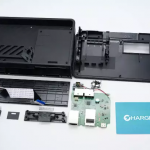
First remove the cover on the side, followed by the screws.

Remove the screws and the back cover.

There is a PCB in the lower right corner for console connecting, video converting. And it can also provide power, peripheral and ethernet connection.

We removed the cover at the bottom and found that the Switch is connected to this PCB module through a flat cable.

Take a closer look.

The metal shields for all ports can be seen on the front of the PCB.

The indicator light is connected to the PCB through red and black wires.

Here is the connection socket for the USB-C connector inside the dock.

The front of the PCBA module is shown in the picture. From the upper left corner to the right are the USB-C port, the HDMI port and the ethernet port. Two USB-A ports at the bottom. Solder the buck converter and filter capacitor, as well as the HUB controller and the ethernet port controller on the front.

Two USB-C controllers, an MCU, memory, and other chips are soldered on the back of the PCB. The USB-A female socket and the ethernet cable socket are soldered by the vias, and the USB-A port is equipped with an independent overcurrent protection chip.

Two synchronous buck converters from TI are on the front, one of which is marked with VUOI, the model is TPS62150, which supports 17V input and 1A output.

Another one is marked with VUNI, the model is TLV62130A, which supports 17V input and 3A output.

These two MOSFETs are connected in series, and used for power supply control of the USB-C port.

A 220μF 10V solid capacitor is used for output filtering.

The USB HUB controller is from VIA Labs, the model is VL210N-Q4.
It can control two USB-A ports, an ethernet port and has low standby power consumption.

The ethernet controller is from Realtek, which is a USB2.0 conversion chip.
Close-up of the external clock crystal oscillator and step-down inductor, marked with RTL8154B.

A video conversion chip is under the metal shield.

It comes from Realtek, the model is RTD2172N, which can convert DP to HDMI.

Connector for connecting the indicator light on the dock.

The USB-C controller is from ROHM, marked with D92B17.

Another USB-C controller is marked with M92T55.

Some MOSFETs for power supply control.

A built-in MCU for the entire dock control from STMicroelectronics, the model is STM32F070RBT6. It integrates an M0 core and 128KB flash.

Close-up of the clock crystal oscillator.

The MCU has an external memory.

The USB-A current limit switch IC is from ROHM, marked with AY, the model is BD2242G, built-in low-impedance MOSFET, the current limit is adjustable from 0.2-1.7A, and supports output discharge.

The other chip is the same model and they are both used for overcurrent protection of the two USB-A ports.

A synchronous step-down converter is from TI, marked with 18N, the model is TLV62568, it supports 5.5V input and 1A output, and it is packaged in SOT563.

A close-up of a resettable fuse.

A close-up of the connection socket connecting the USB-C.

Close-up of the USB-C connector.

Close-up of the HDMI connector.

Close-up of the ethernet connector, there is no connection indicator.

Close-up of USB-A connectors, with a unibody design.

The inside of the USB-C connector is supported by springs.

Close-up of the spring.

USB-C is fixed with screws.

Full pin design, SMD pin soldering.

On the back of the small PCB is the solder pad for USB-C.

Finally, let's disassemble the indicator lights inside the dock.

The indicator light is soldered on the small PCB and connected by wires and connectors.

Colorful cables for indicator light.

Same thing on the back.

That's all for the teardown.
Summary of ChargerLAB
The Nintendo switch OLED changes the USB3.0 port to an ethernet port. When connecting to the dock, the network connection is more stable and can also improve the connection speed and game experience.
Related Articles:
1. Teardown of Original Nintendo Switch Charging Dock
2. Teardown of HAGiBiS 65W GaN Charger Dock With HDMI (For Nintendo Switch)
3. Teardown of Original Nintendo Switch OLED Model Charging Dock

