Introduction
Fast charging can greatly improve the charging experience of mobile phones. And the 100W or higher power adapter can even fast charge the phone within 20mins. Motorola's recently released MOTO X30 Pro comes with a 125W GaN fast charger.
The MOTO X30 Pro can be charged 50% in 7 minutes and fully charged in 19 minutes with this charger. And it also supports 100W PD fast charging, which is convenient for charging your laptop and other devices. Let's take it apart and see what it looks like inside.
Unboxing
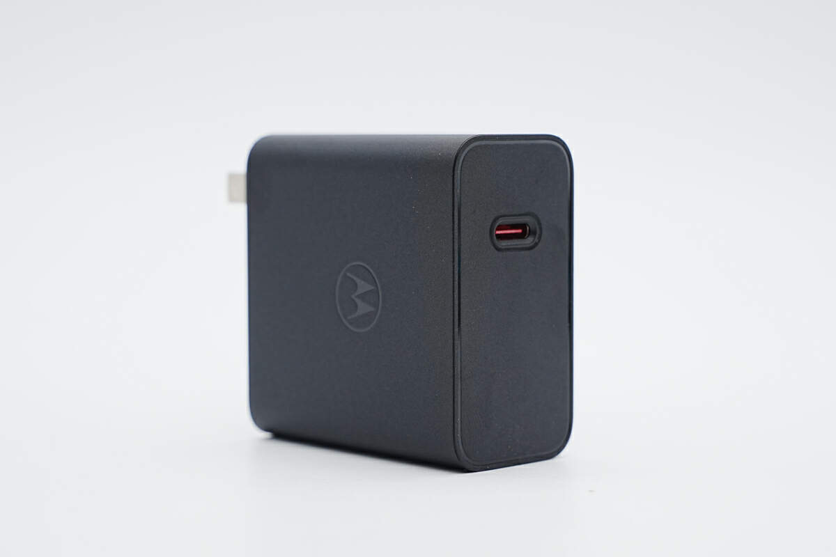
This charger adopts black matte shell, which can effectively resist fingerprints.
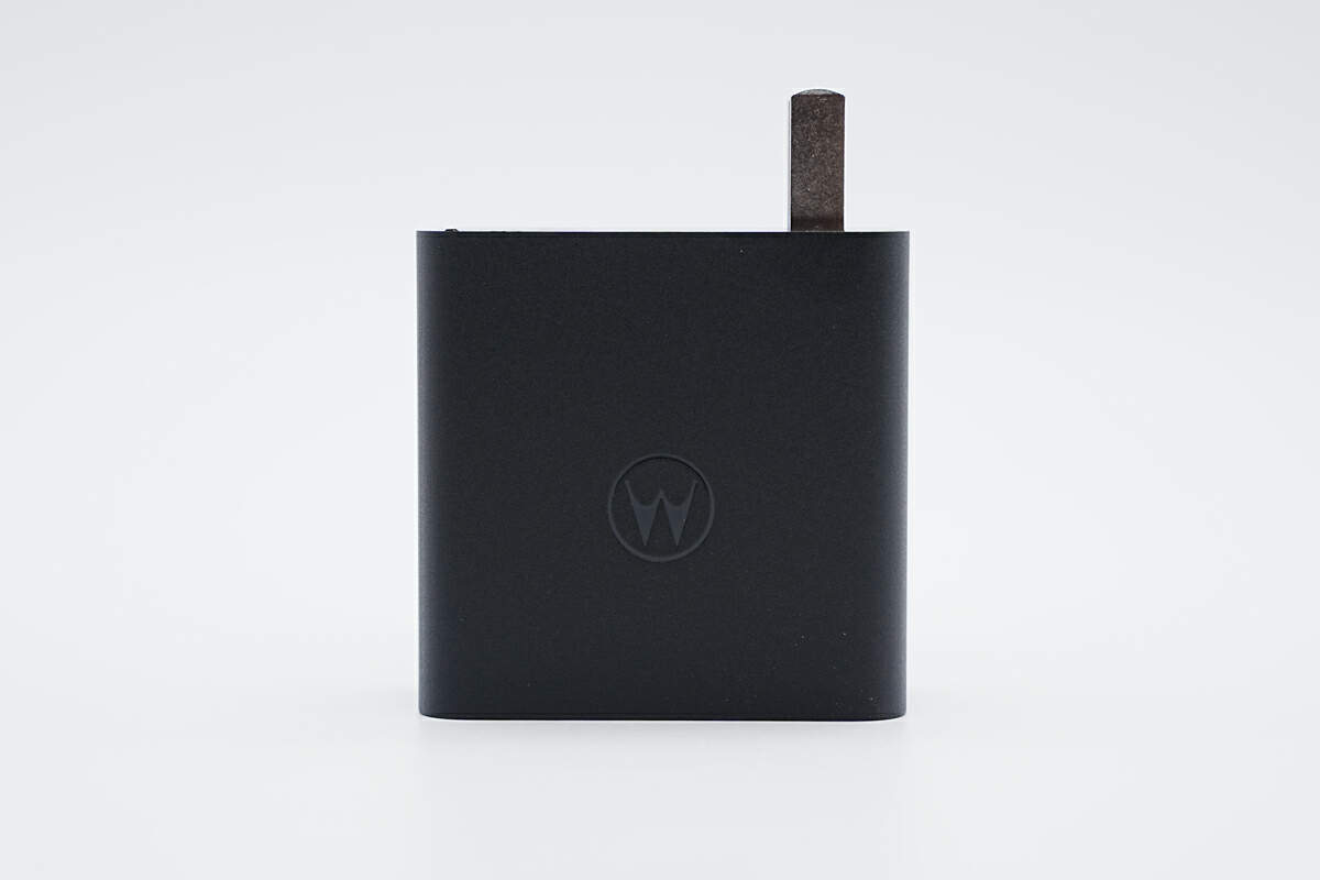
And the Motorola brand logo is in the middle.
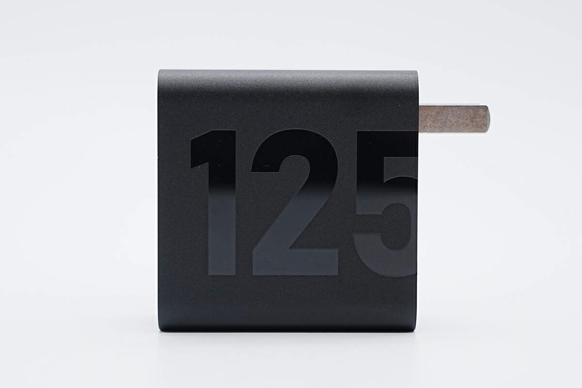
The 125W is printed on the other side. And the input prongs cannot be folded.
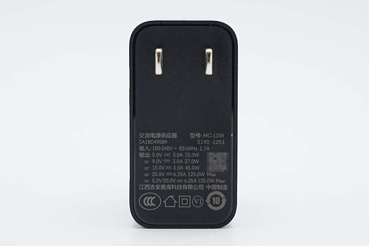
All specs info are printed at the bottom. Model is MC-1258.
It can support input of 100-240V~50/60HZ 1.7A and output of 5V3A, 9V3A, 15V3A, 20V6.25A, and 5-20V6.25A. The manufacturer is Aohai Technology.
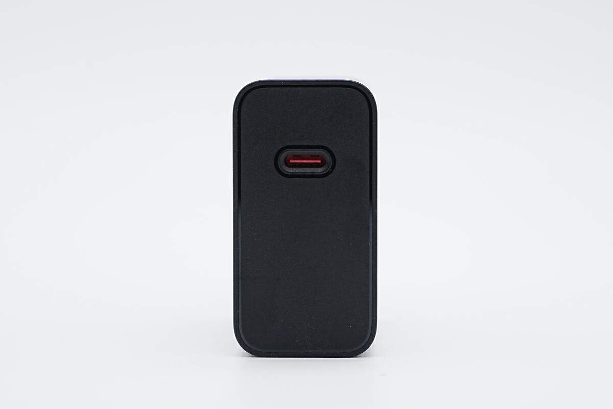
There is only one USB-C port, and the internal plate is red. Pretty striking.
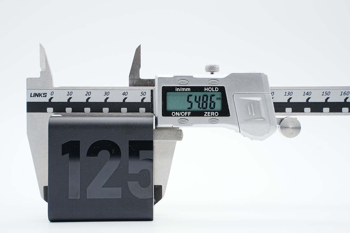
The length of this charger is 54.86mm (2.16 inches).
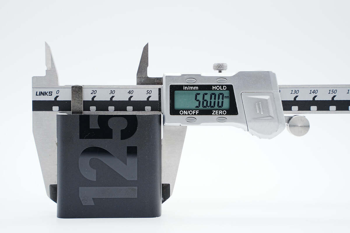
The width is 56mm (2.2 inches).
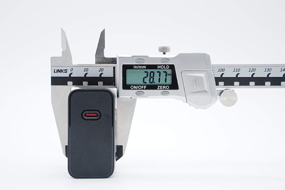
And the thickness is 28.77mm (1.13 inches).
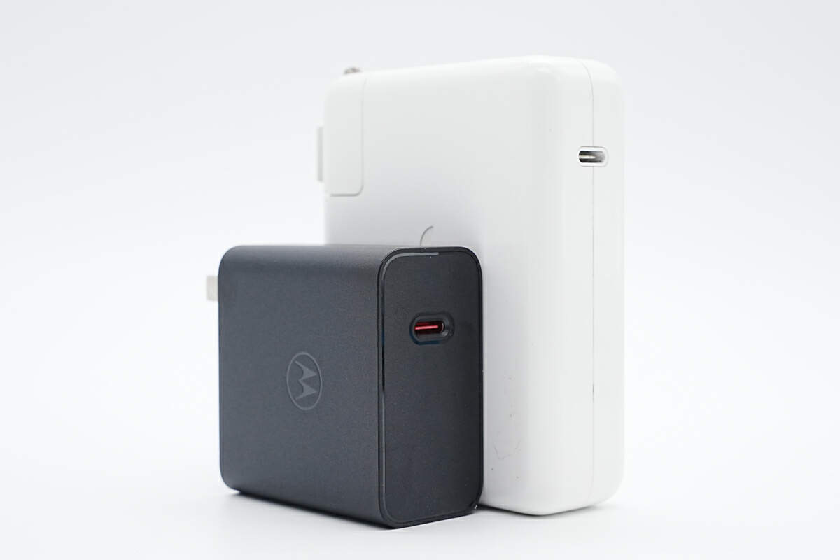
Compared with Apple 140W charger, the size is much smaller.
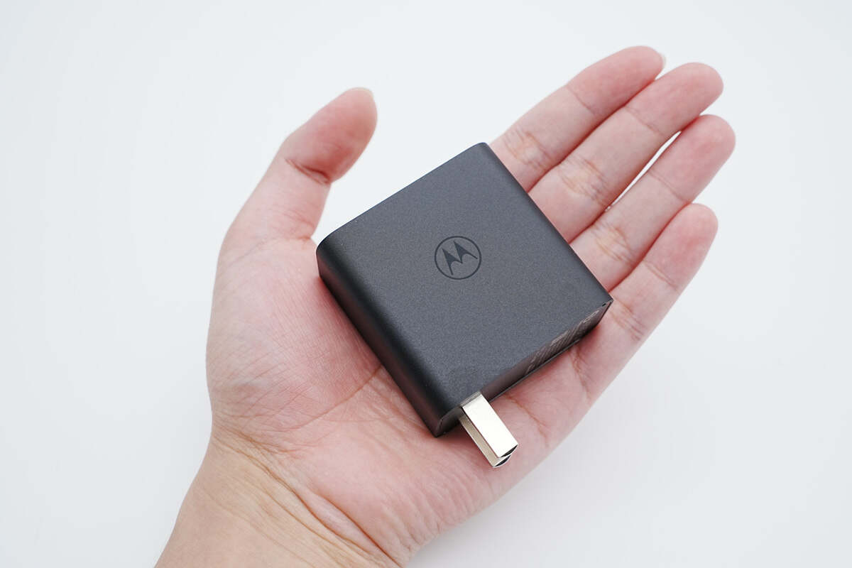
That's how you hold it.
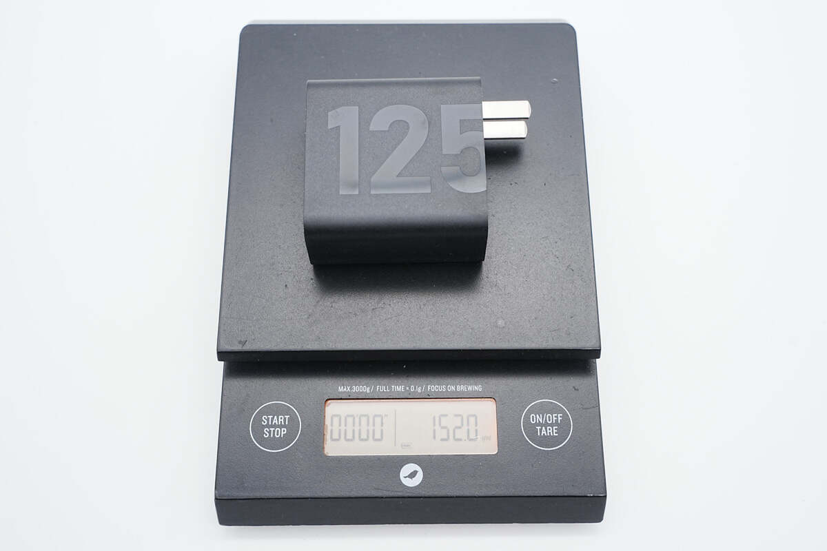
And the weight of this charger is 152g (5.36 oz).
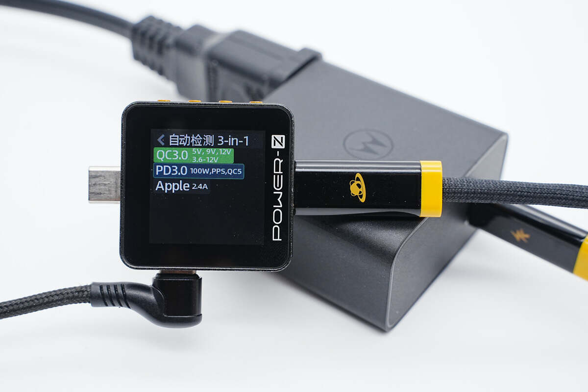
The ChargerLAB POWER-Z KM002C shows the USB-C supports QC3.0, PD3.0, PPS, QC5, and Apple2.4A protocol.
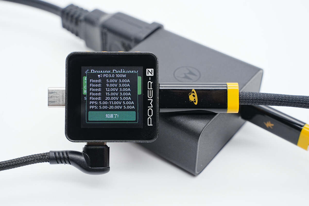
It also supports five fixed PDOs of 5V3A, 9V3A, 12V3A, 15V3A, 20V5A, and two sets of PPS of 5-11V5A, 5-20V5A. Except for this, it also supports 20V 6.25A, which is the MOTO private protocol.
Teardown
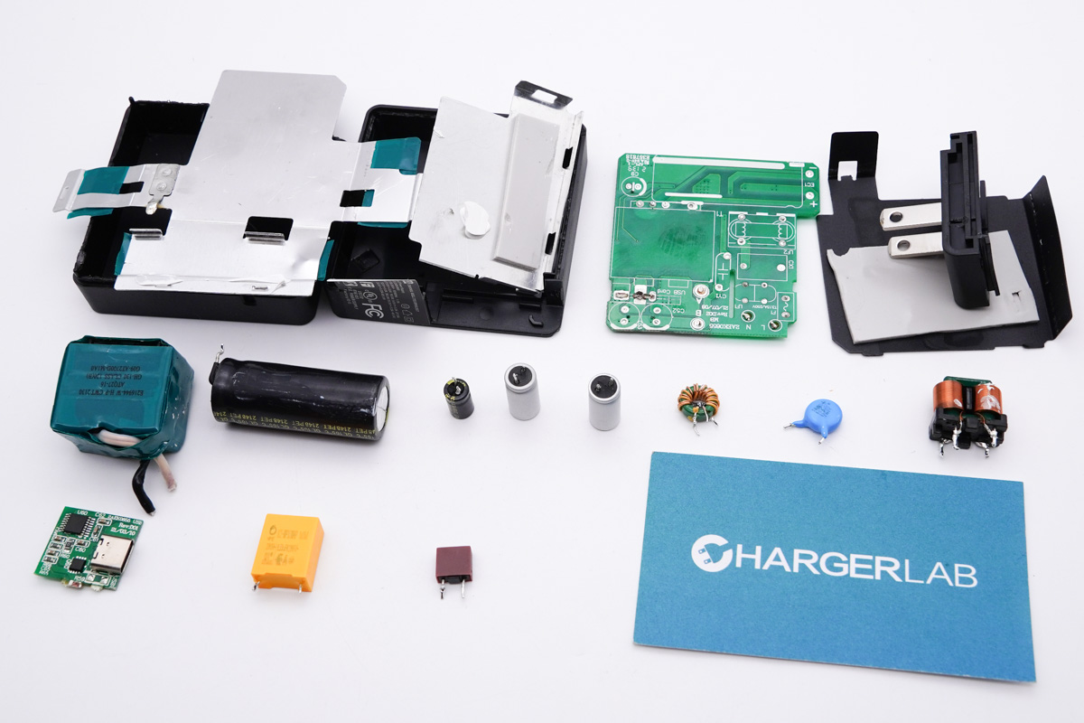
After the brief introduction and size measurement, let's go ahead and take it apart to see its internal components.
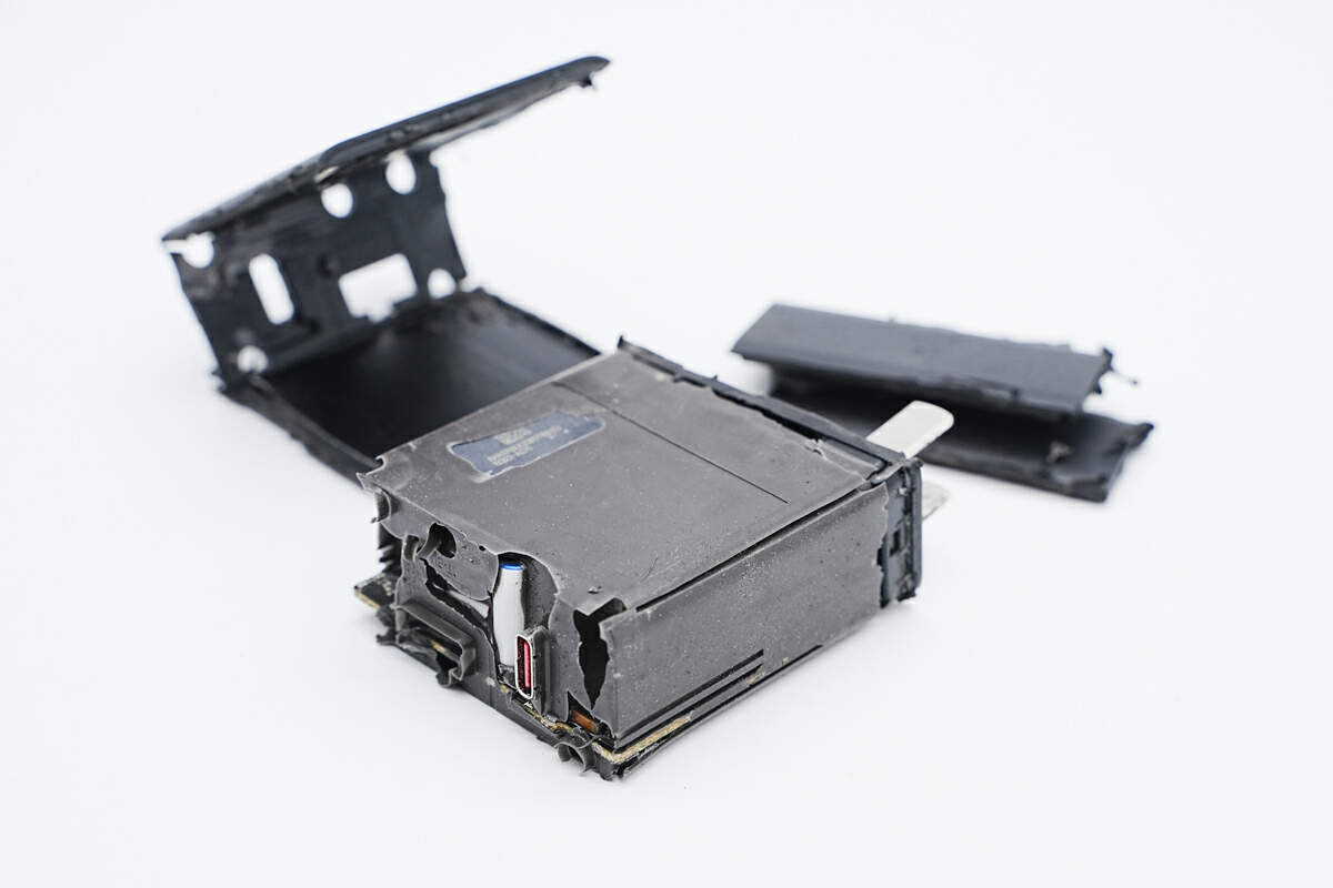
Use the cutting machine to separate the shell. The entire PCBA module is covered with silicone adhesives.
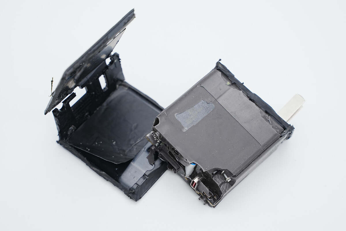
The graphite thermal sheet is pasted inside the shell to enhance heat dissipation.
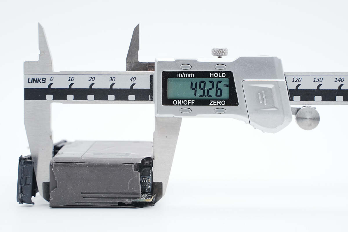
The vernier caliper shows the length of the PCBA module is 49.26mm (1.94 inches).
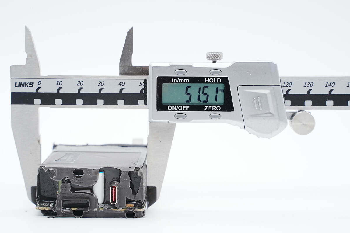
The width of the PCBA module is 51.51mm (2.03 inches).
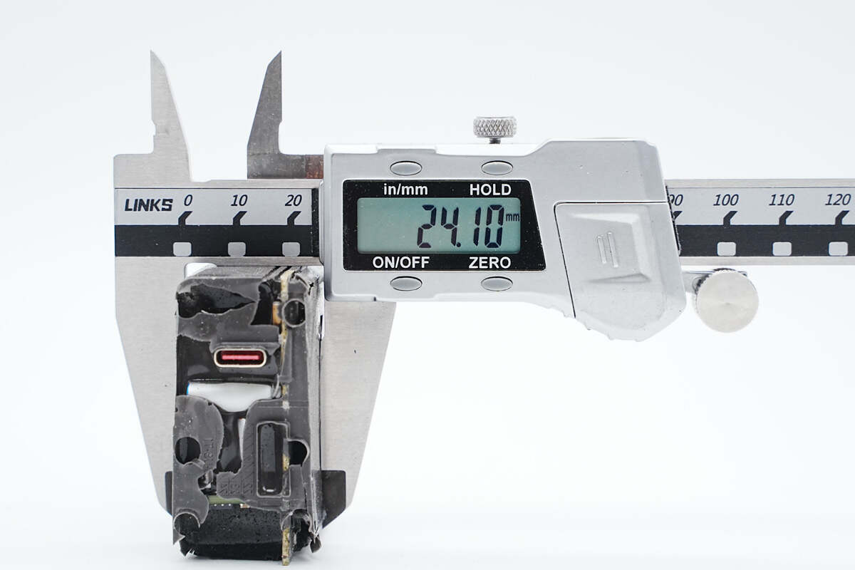
The thickness of the PCBA module is 24.1mm (0.95 inches).
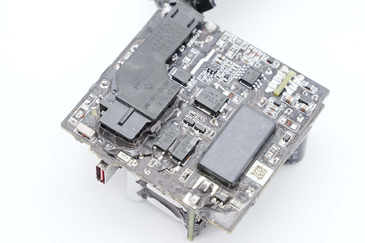
Clean up the PCBA module. The back of the PCBA module is pasted with insulating plastic cover. And the planar transformer is placed in the hollow of the PCB to reduce the thickness.
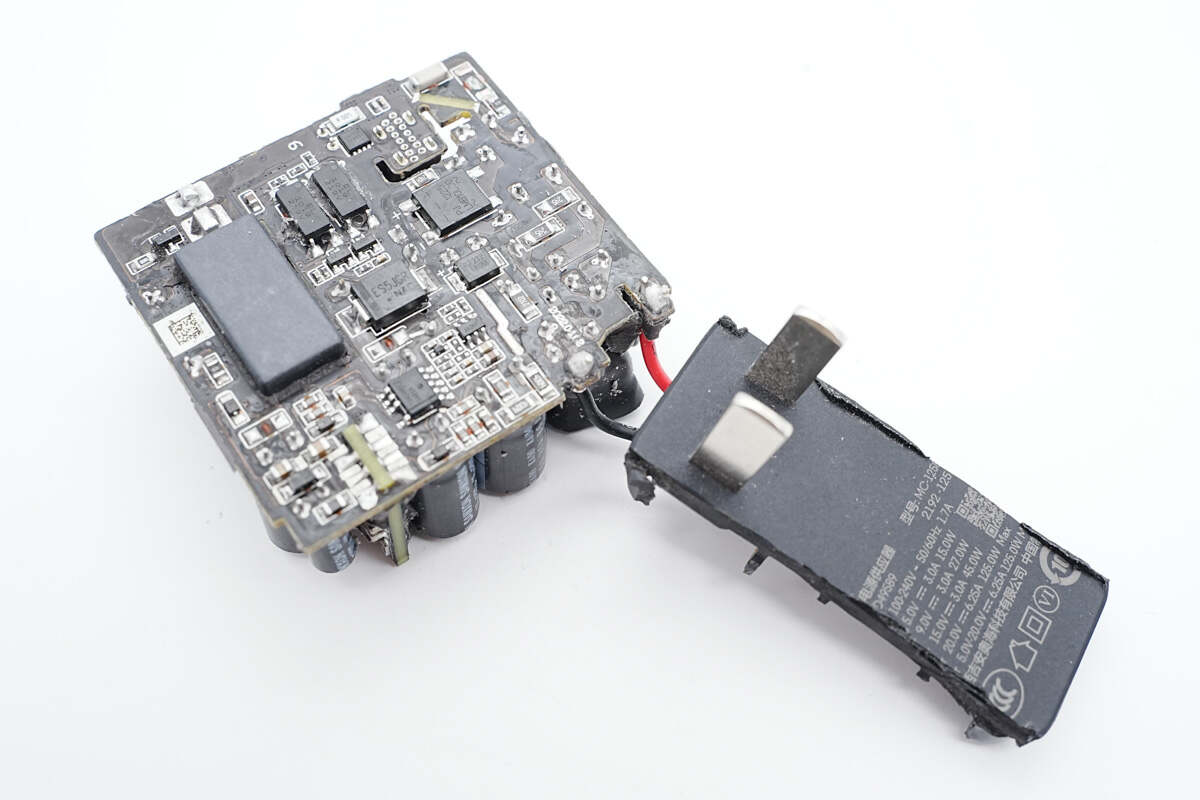
The red and black wires are connected to the AC input.
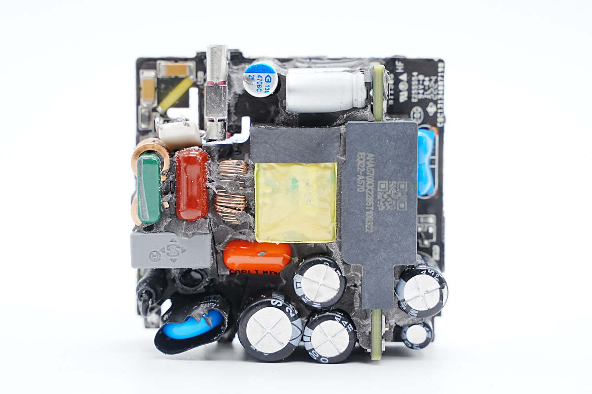
Here is the front of the PCBA module. The input EMI circuit is in the lower left corner. And the PFC inductor is in the center. The planar transformer is on the right side, and the output end is at the top.
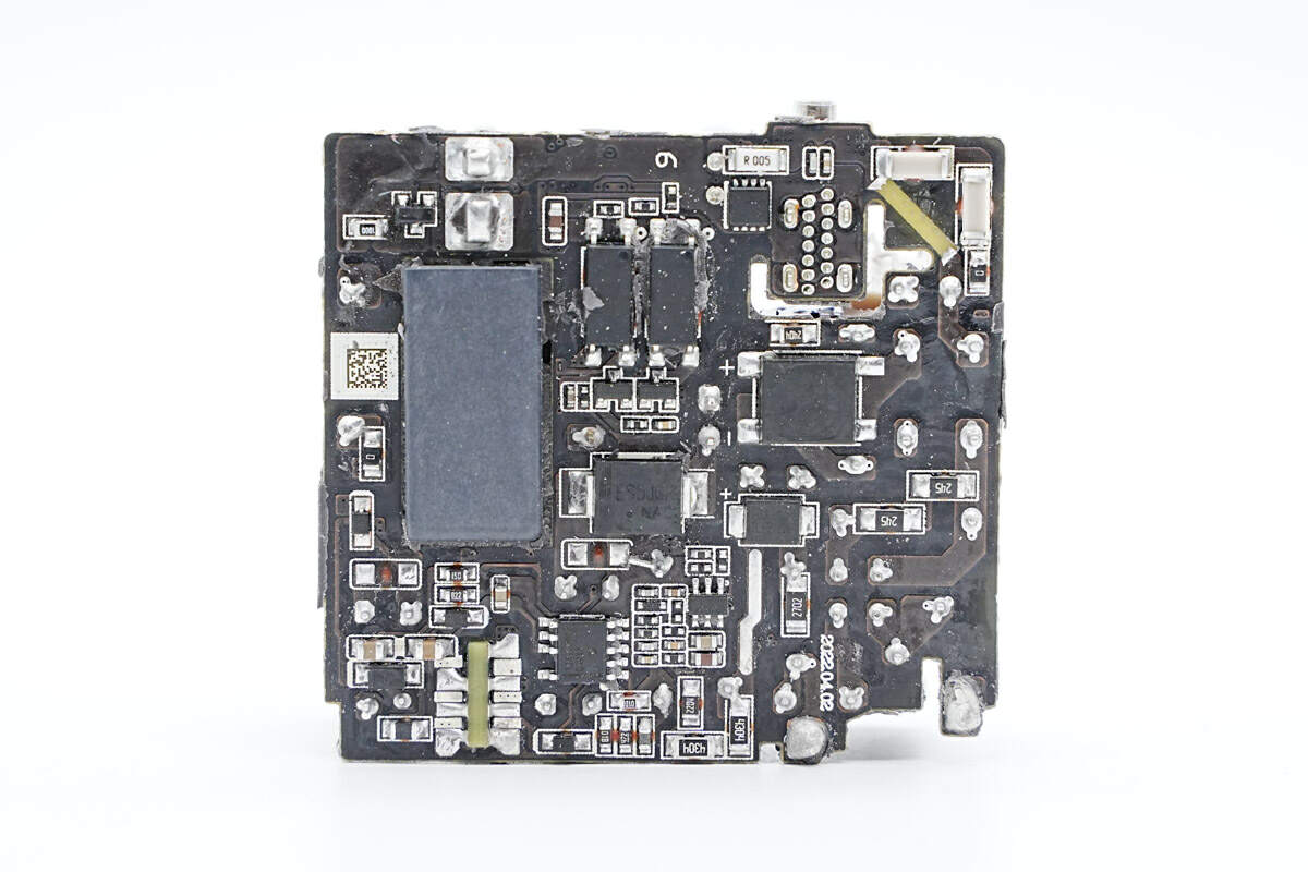
Flip to the back. We can find the bridge rectifier, PFC and flyback controller, two optocouplers, current sampling resistor, and VBUS MOSFET.
ChargerLAB found that this charger consists of PFC boost circuit and QR flyback topology. The output voltage is regulated by the optocoupler and controlled by the protocol chip. Let's start from the input end to introduce every single component.
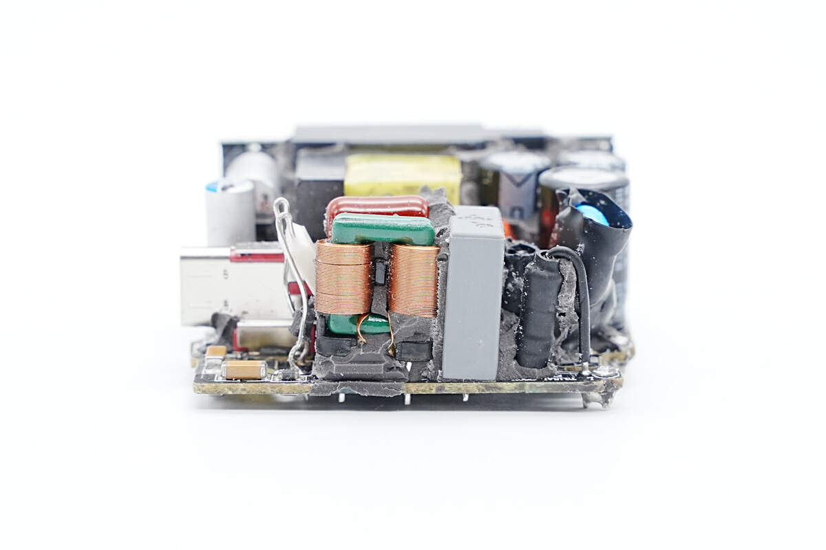
Here is the input end. We can find the fuse, NTC thermistor, varistors, common mode choke, safety X2 capacitor, etc.
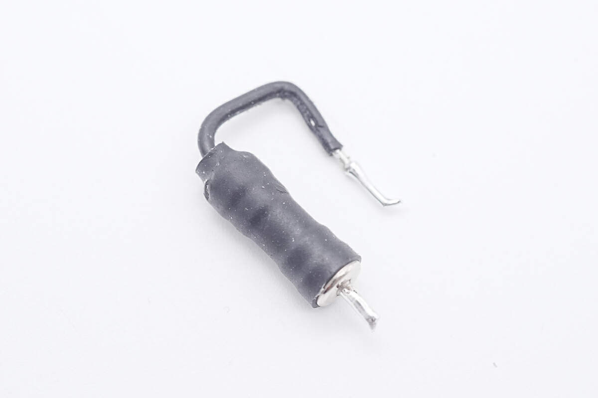
The input fuse is insulated with heat shrinkable tube.
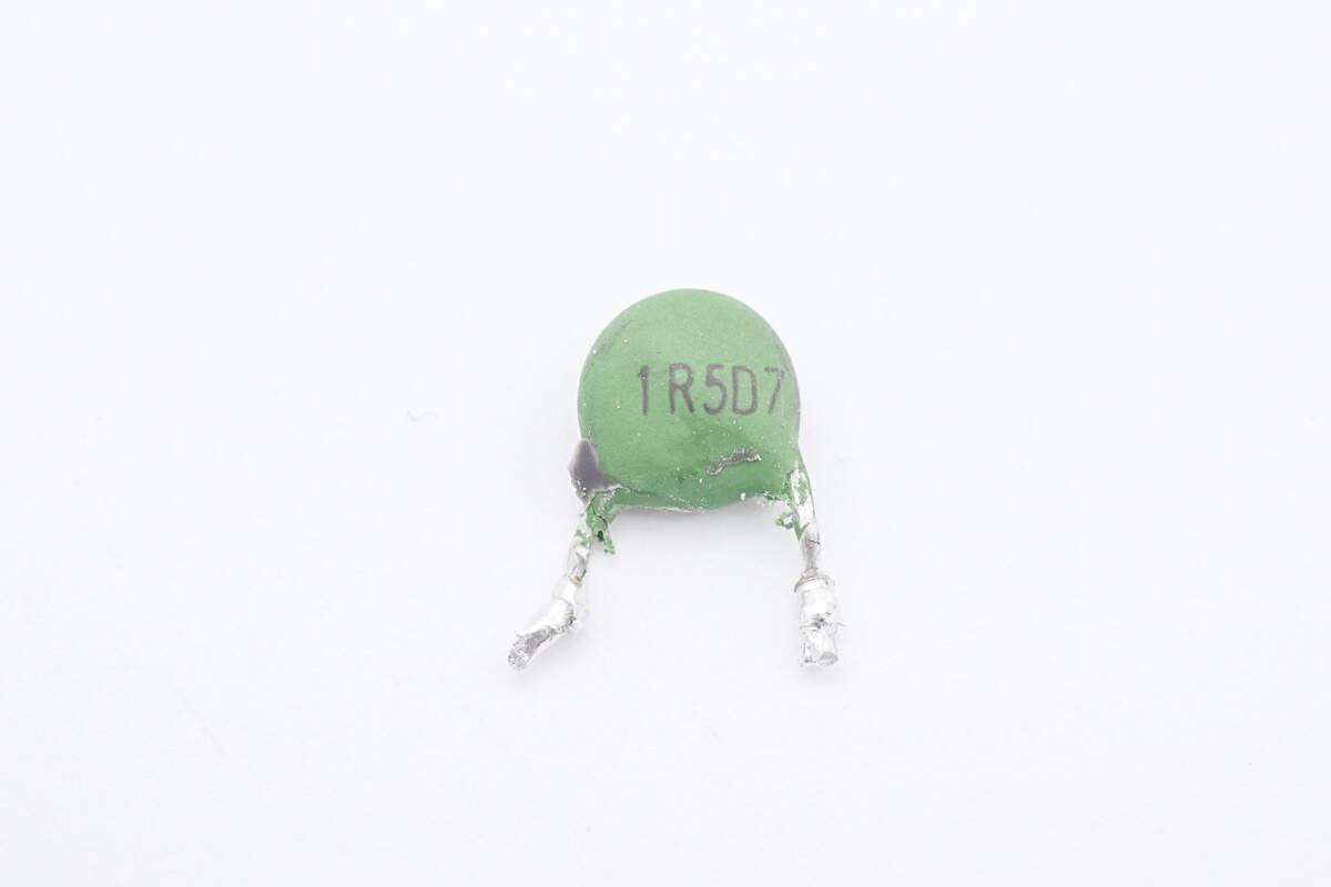
The green NTC thermistor is used to suppress inrush current and reduce sparking when plugged it into the outlet. The diameter is 7mm, and cold resistance is 1.5Ω.
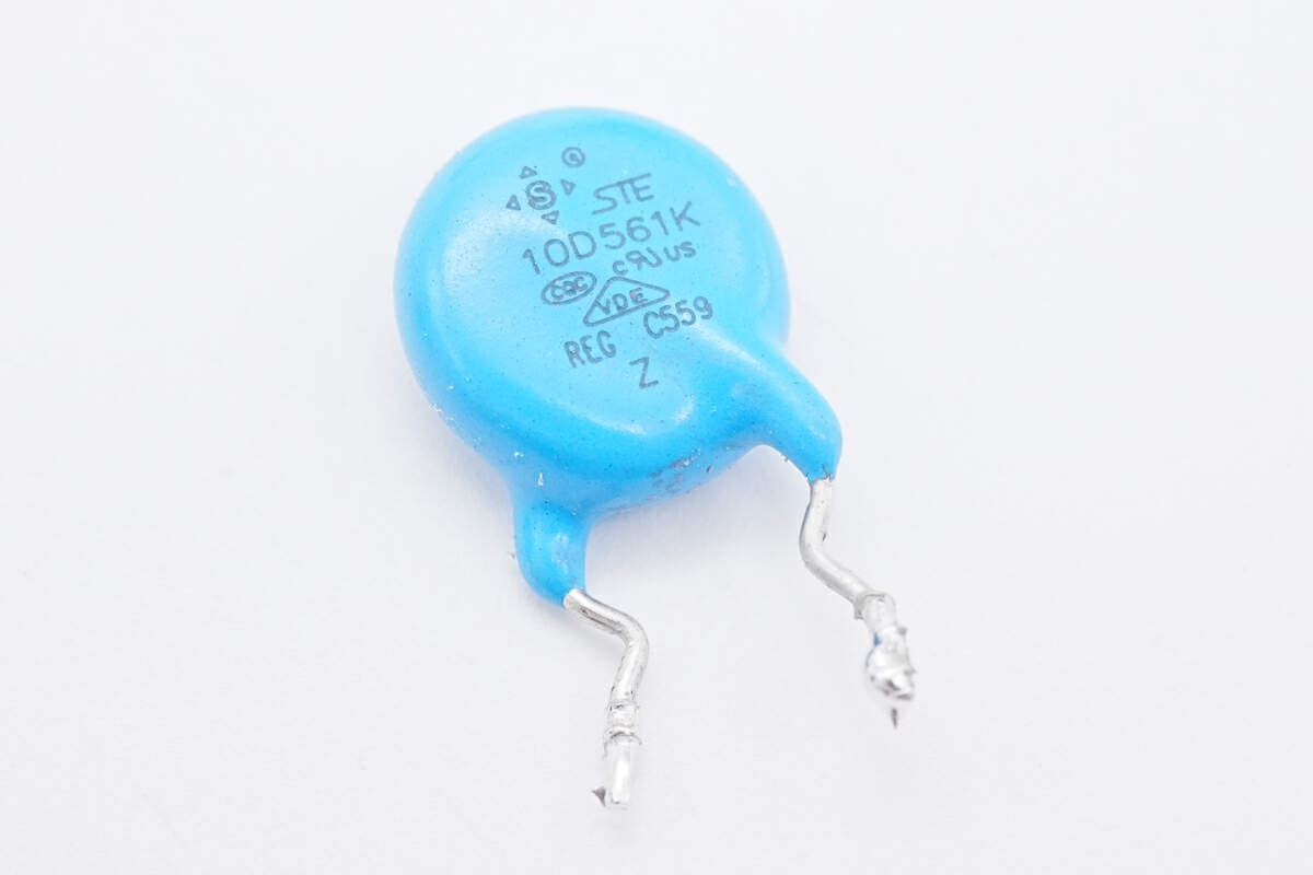
The blue varistor is from STE, marked with 10D561K. It's used for input overvoltage protection.
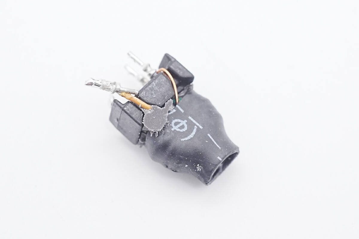
The first common mode choke is wound with different wires and insulated with heat shrinkable tube.
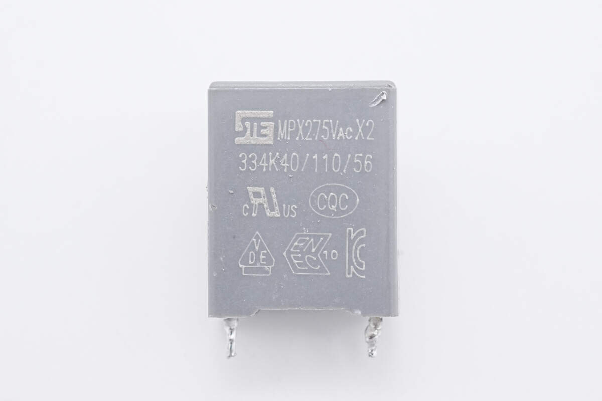
The safety X2 capacitor is from STE with a capacity of 0.33μF.
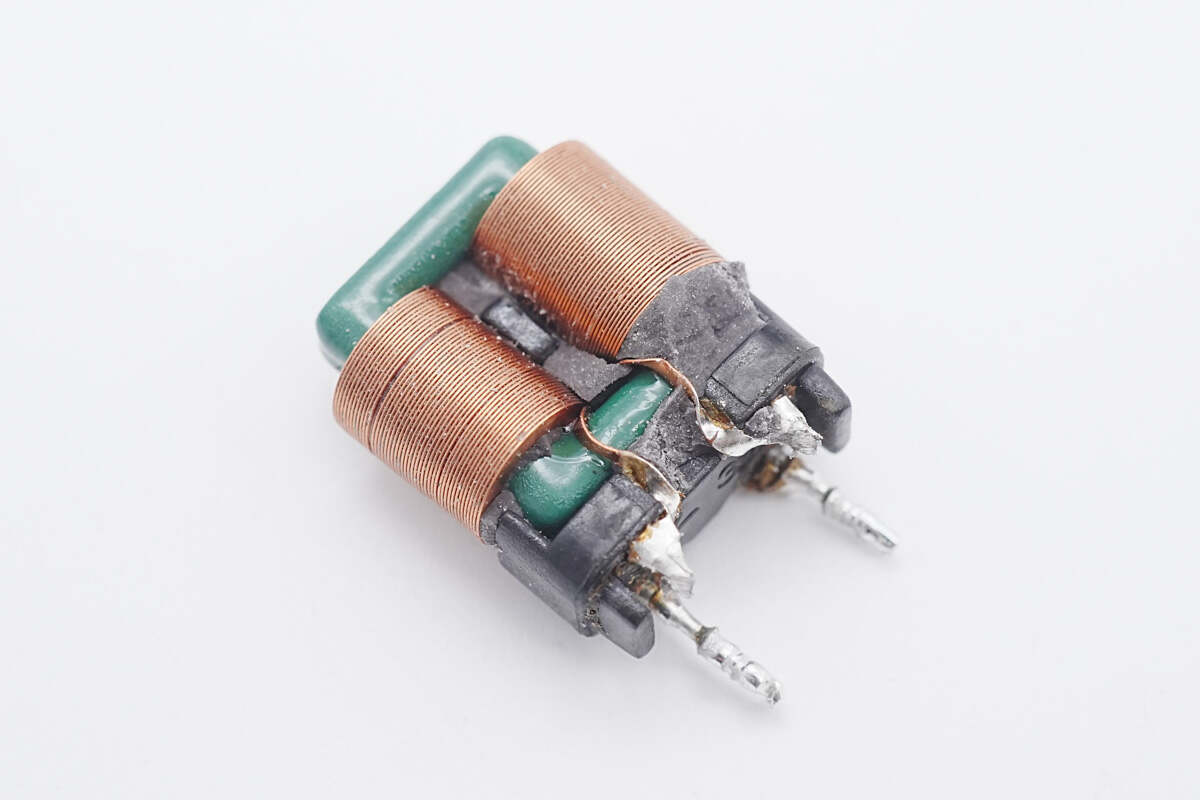
The second common mode choke is wound with flat copper wire.
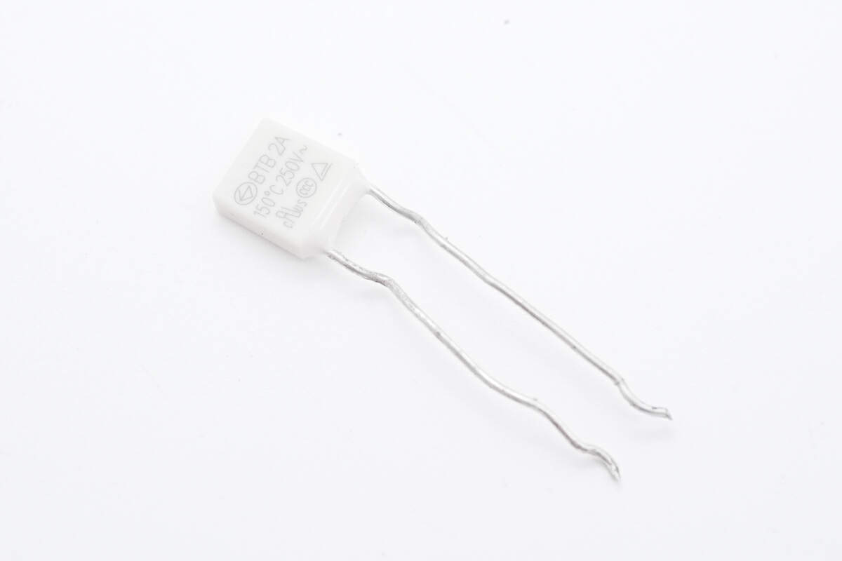
The thermal fuse is from Better Electronics. And the melting temperature of 150°C. It is fixed on the common mode choke to detect the temperature and is used for overheating protection.
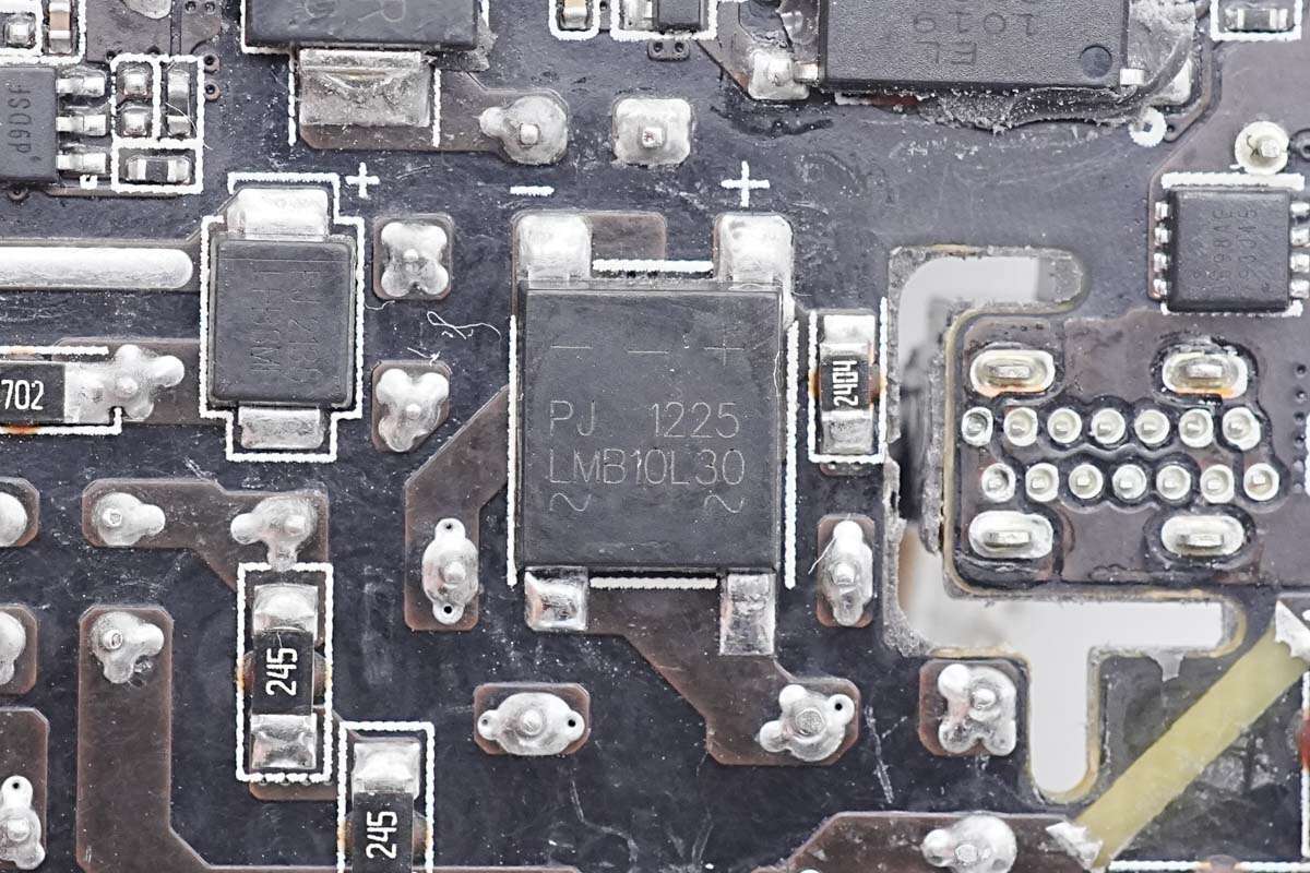
Two bridge rectifiers are soldered on the front and back of the PCB, which can dissipate heat evenly and reduce the temperature.
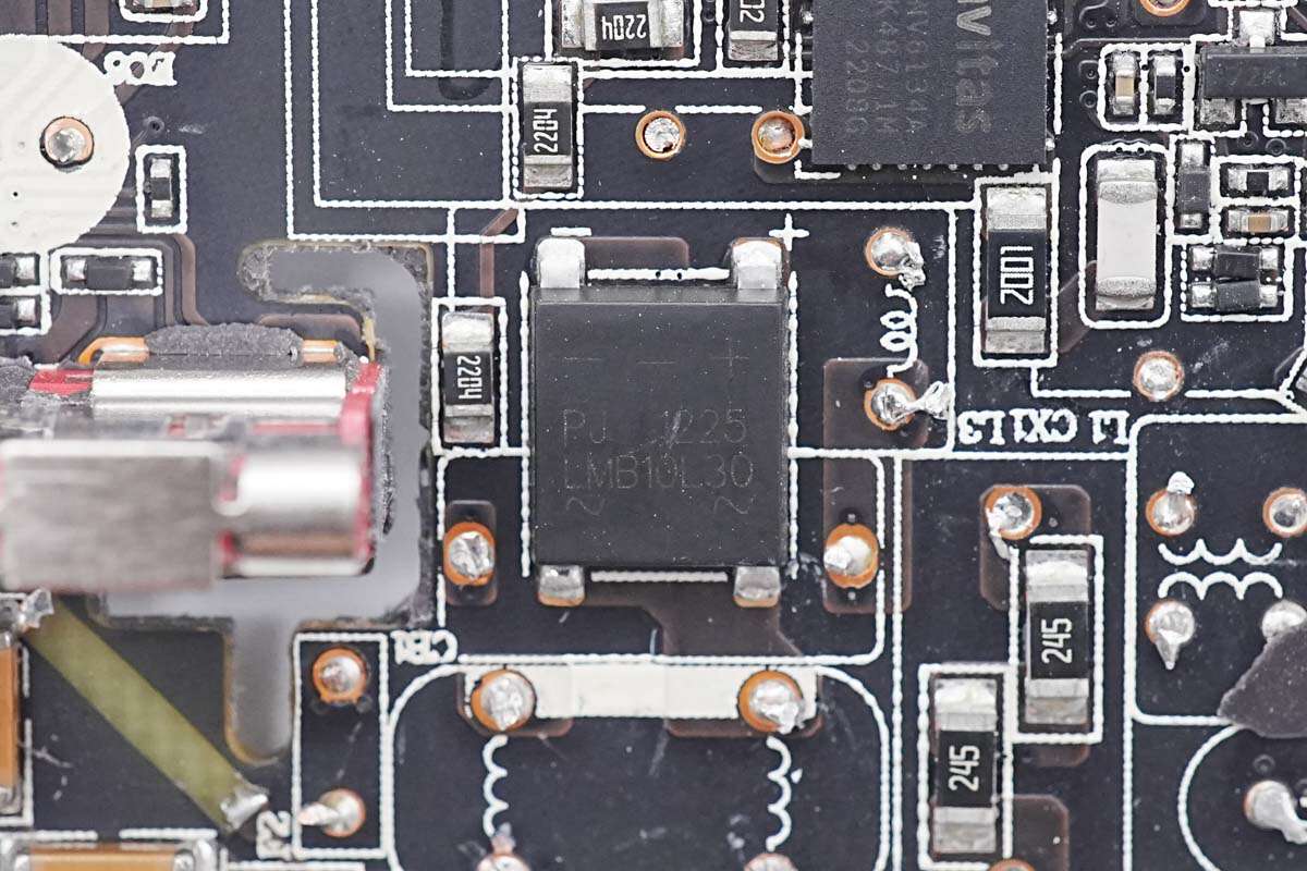
They're marked with LMB10L30 and used to convert AC to pulsed DC.
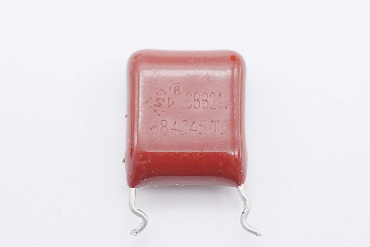
The red film capacitor is from STE and is used for output filtering. 0.68μF 450V.
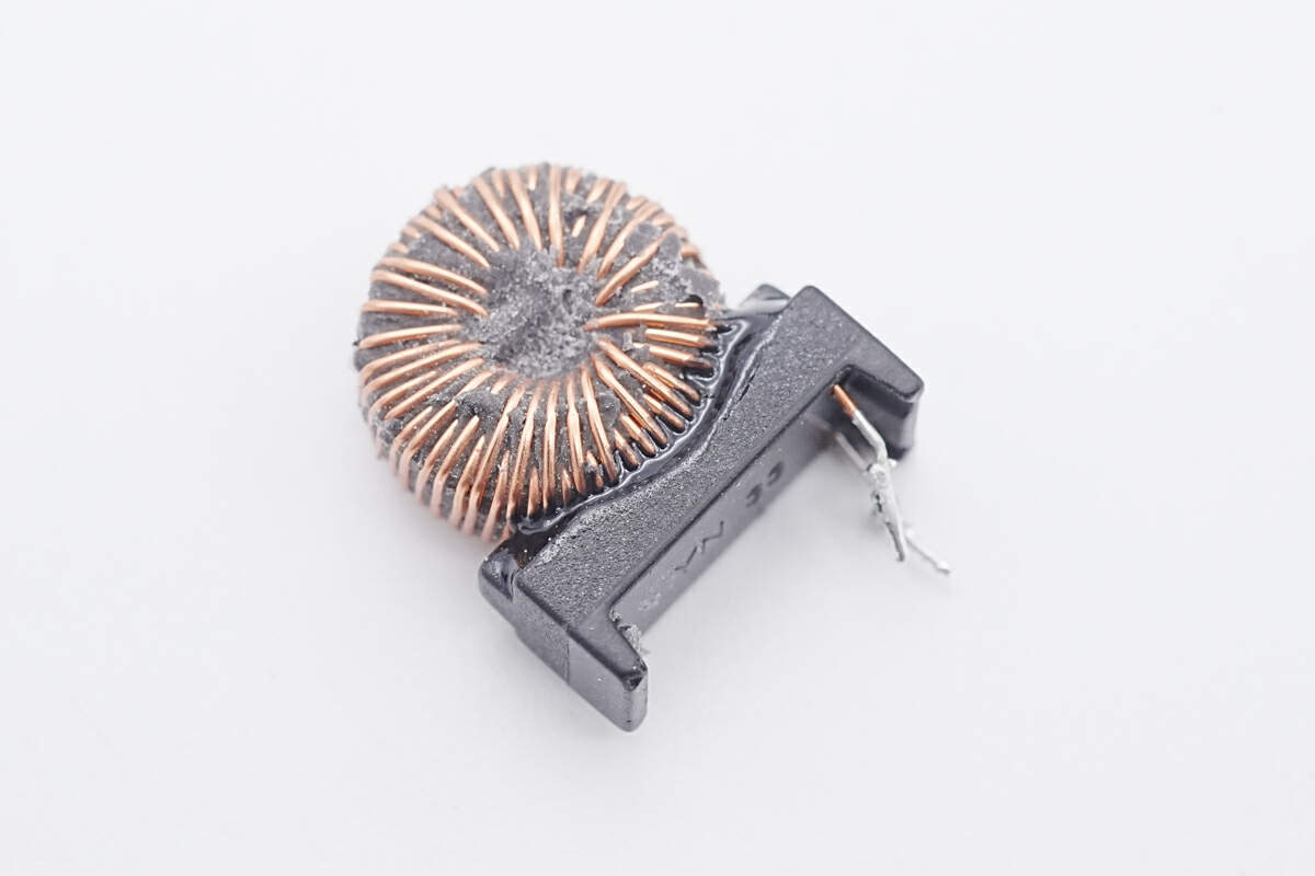
The toroidal-core inductor is also used for output filtering.
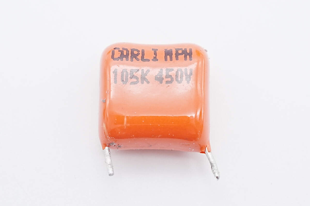
Another film capacitor is from CARLI. 1μF 450V.
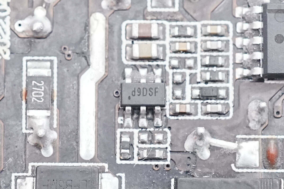
The PFC boost controller is from Silergy SY5072B, which is a PFC controller operating in critical mode. It drives the boost converter in the Quasi-Resonant mode for high efficiency and better EMI performance.
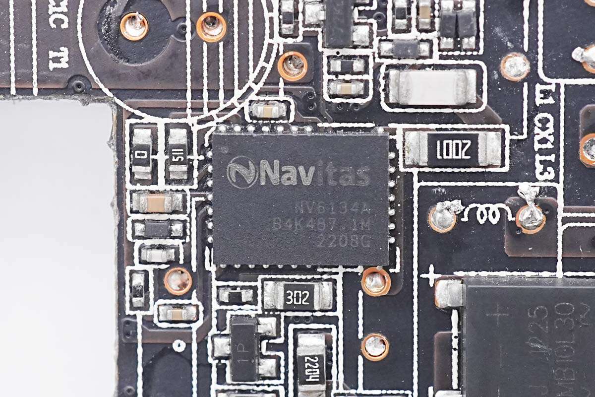
The PFC boost transistor is from Navitas NV6134A, which is the latest GaN power IC of the GaNFast series. It integrates GaNSense lossless current sampling technology, and no external resistor is required, which improves charger efficiency, reduces heat, and can save more space. It also has over-temperature, over-current, and other protections, ensuring the charger's reliability.
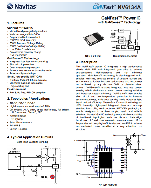
Datasheet of Navitas NV6134A.
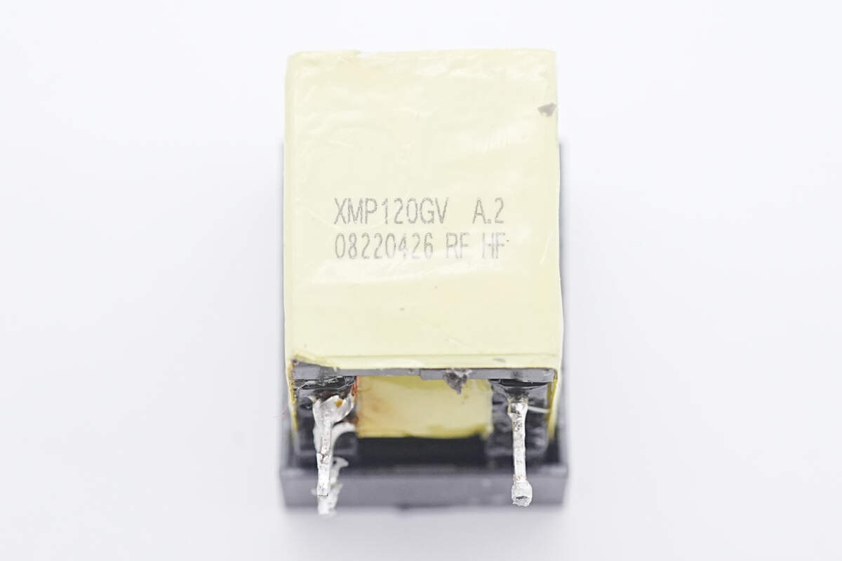
The PFC boost inductor is covered with a plastic case for insulation.
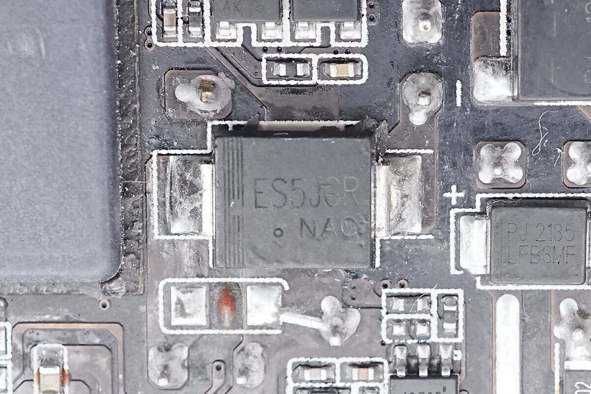
Here is the fast recovery diode for PFC rectification.
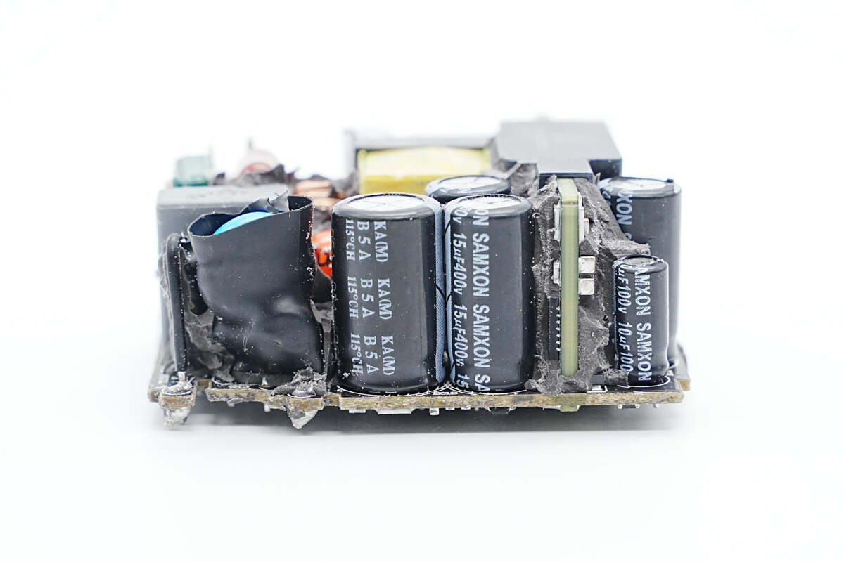
Here're electrolytic capacitors for high-voltage filtering and a small power supply capacitor.
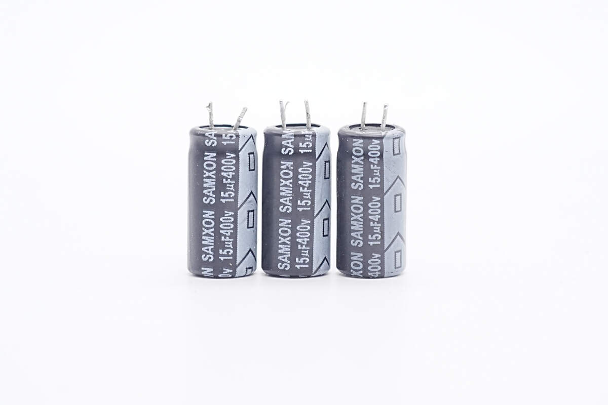
Those three input capacitors are all from SAMXON.
400V 15μF.
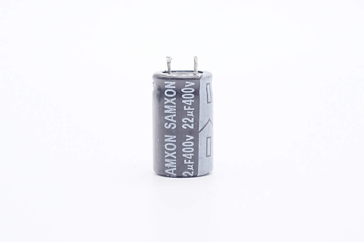
The other one is 400V 22μF.
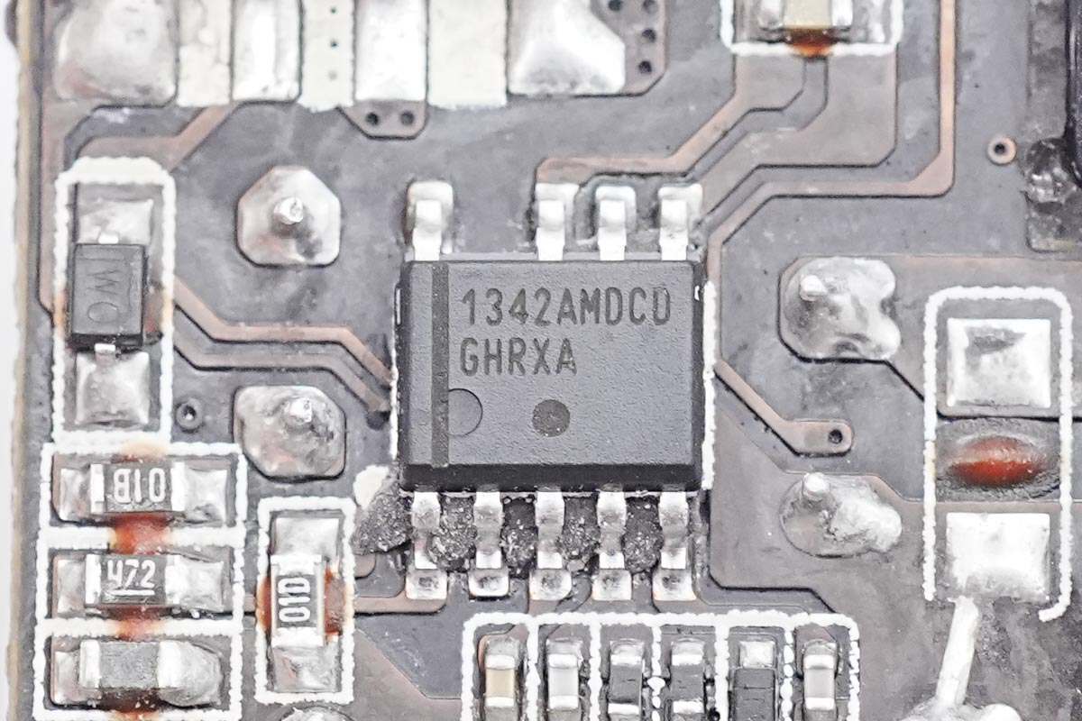
The primary controller is from ON Semiconductor NCP1342, which is a high-frequency QR flyback PWM controller. It integrates high-voltage startup and active X2 capacitor discharge features. And it can support wide range of Vcc power supply, external thermistor for overheating protection, and multiple protection functions.
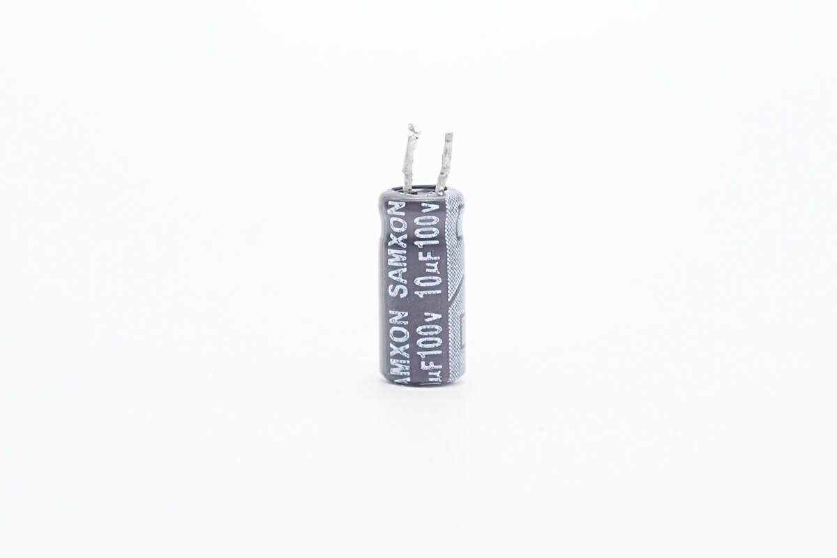
Here is the power supply capacitor for powering the PFC and primary controller. 100V 10μF.
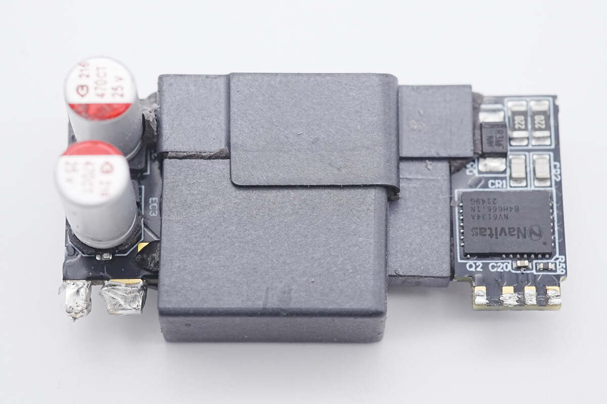
Since it adopts the planar transformer, some components are soldered on both sides to improve power density. Two solid capacitors are on the secondary side. And a Navitas GaN power IC is on the primary side.
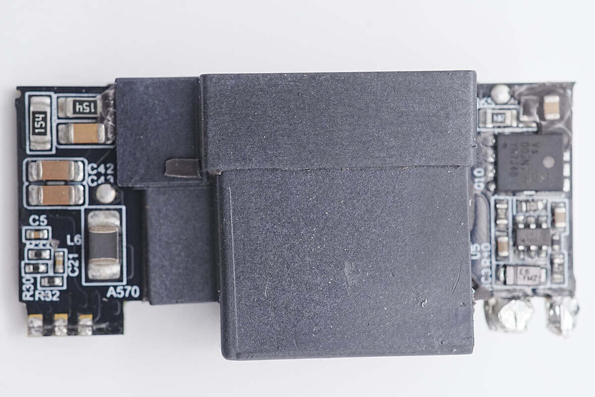
Flip to the back. The synchronous rectifier and its controller are on the secondary side, while the RCD clamping circuit is on the primary side.
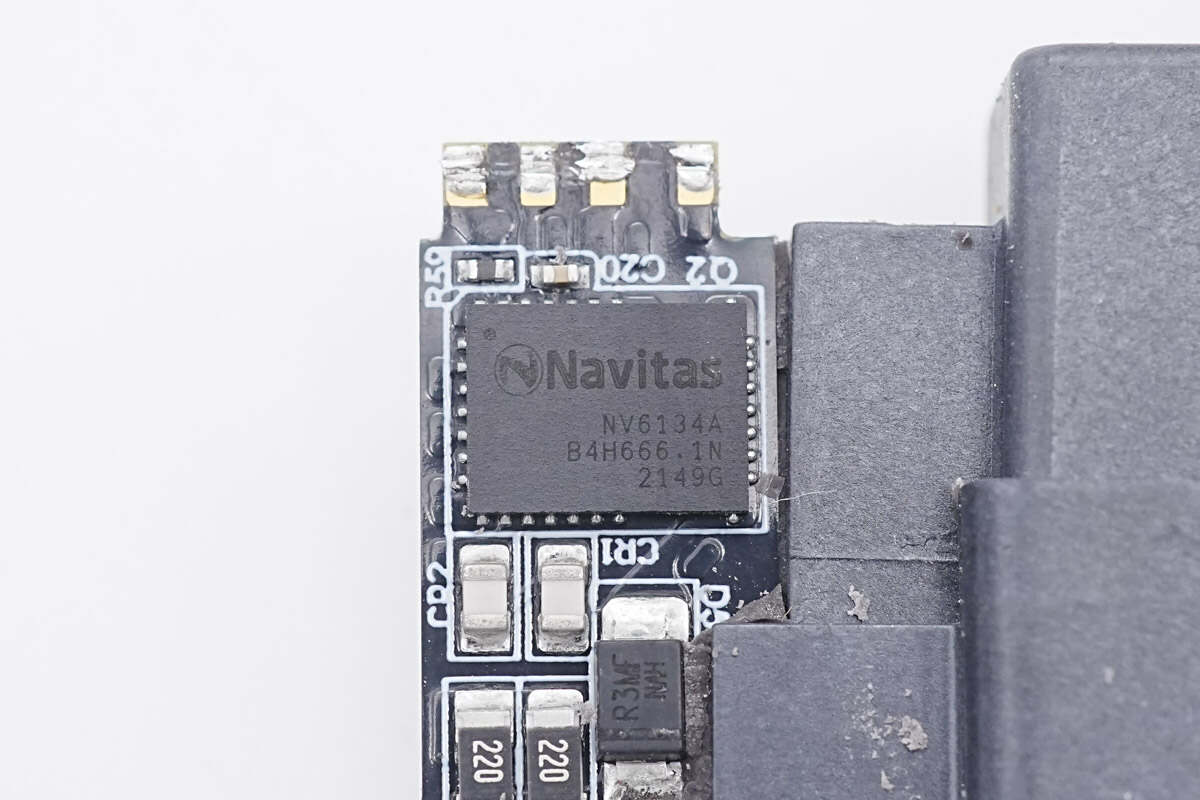
The primary GaN power IC is also from Navitas NV6134A, same as the PFC circuit. So, there're two Navitas GaN power ICs inside this charger.
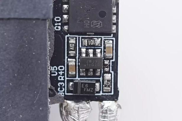
The synchronous rectifier controller is from Joulwatt JW7726B, which can support CCM, DCM, QR, and ACF modes. It can effectively prevent the gate from being coupled to the turn-on voltage during startup.
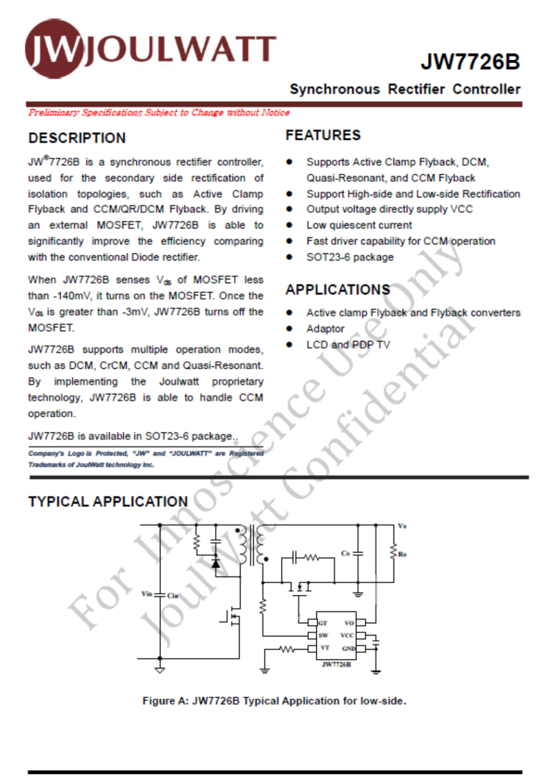
Datasheet of Joulwatt JW7726B.
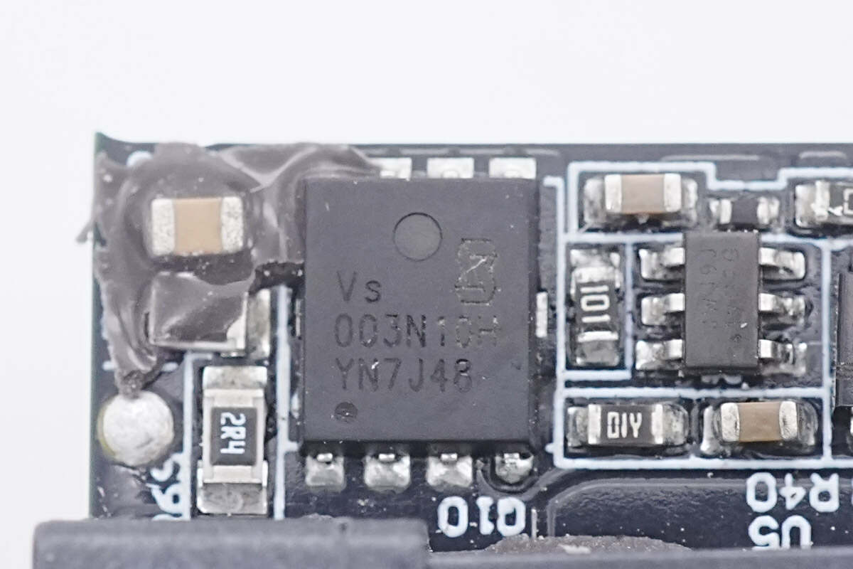
The synchronous rectifier is from Vergiga VSP003N10HS-G and adopts PDFN5 x 6 package. Withstand voltage is 100V and resistance is 3.8mΩ.
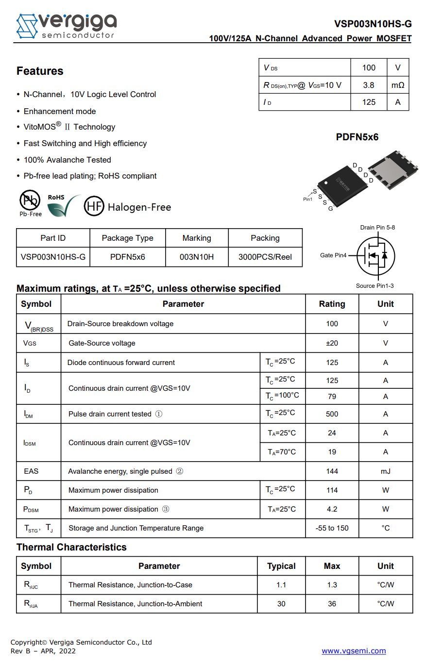
Datasheet of Joulwatt JW7726B.
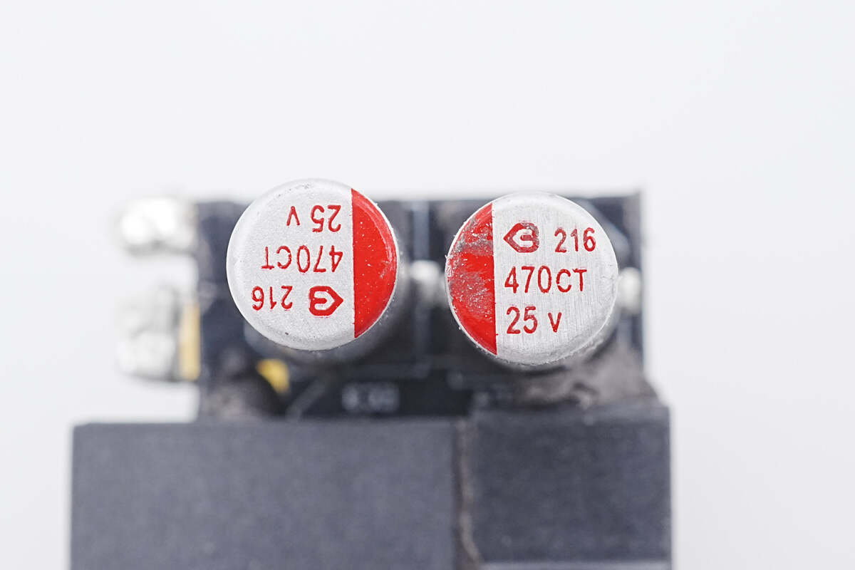
Two solid capacitors for output filtering are from BERYL electronics.
They're connected in parallel with specifications of 470μF 25V.
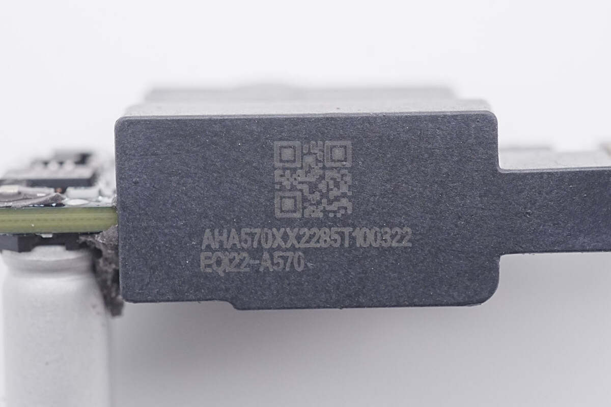
A QR code and other info are printed on the side of the magnetic core.
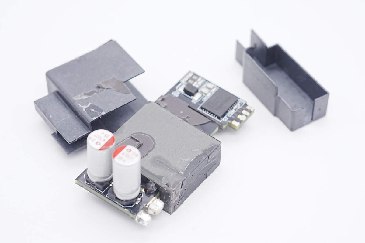
Remove the plastic case, and we can see the magnetic core.
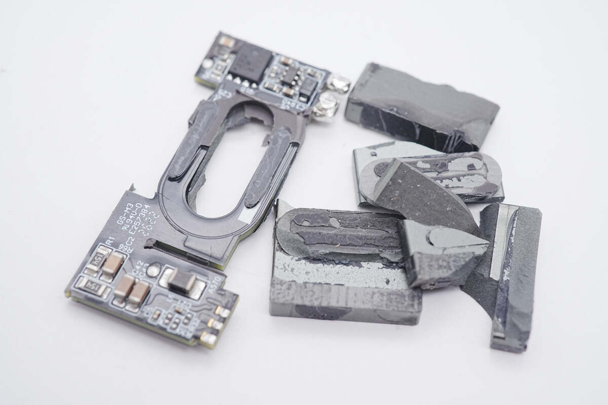
Smash the magnetic core, and we can see the coils inside.
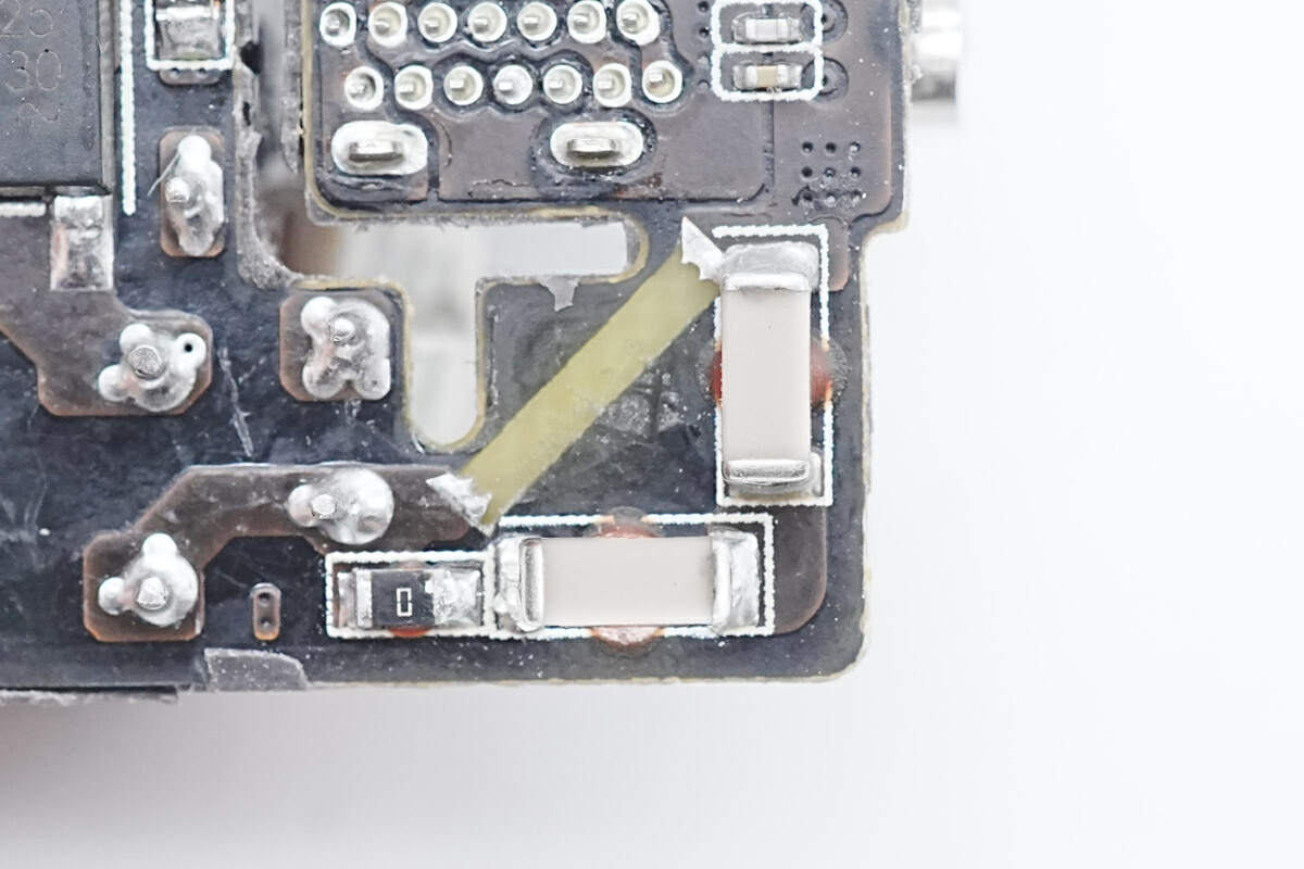
Two sets of SMD Y capacitors are connected in series to improve the safety level.
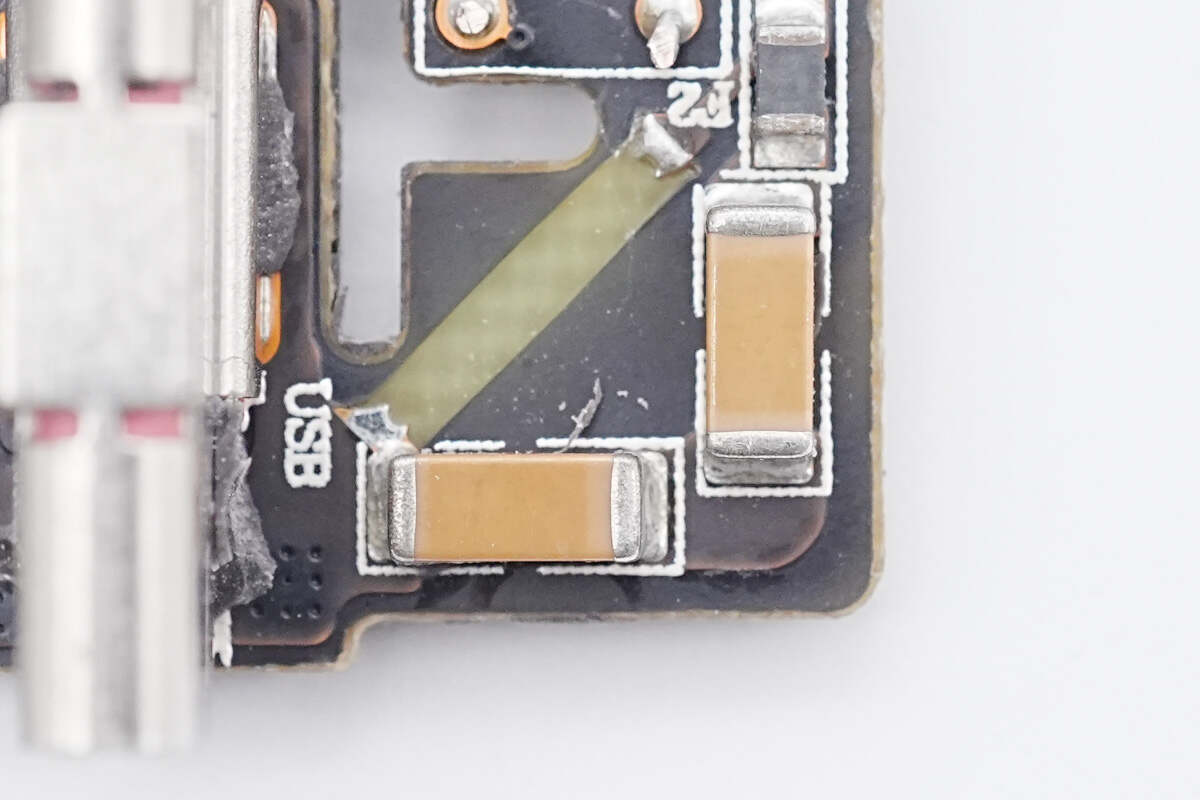
Another set of SMD Y capacitors are connected in series.
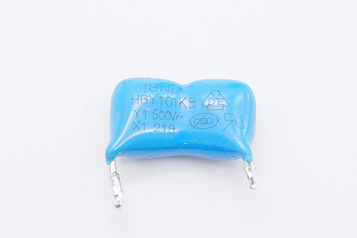
The blue Y capacitor is from iSND.
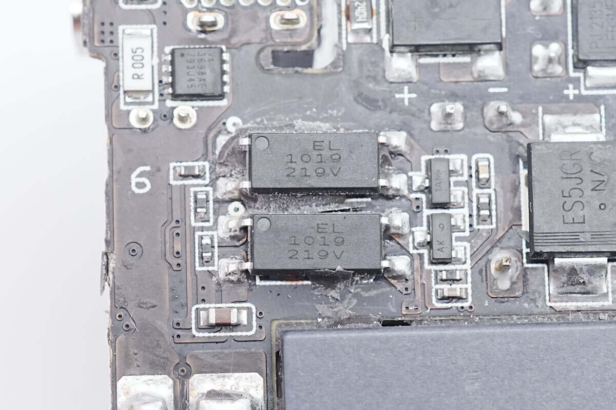
Two EL1019 optocouplers are used to regulate the output voltage and control the PFC circuit.
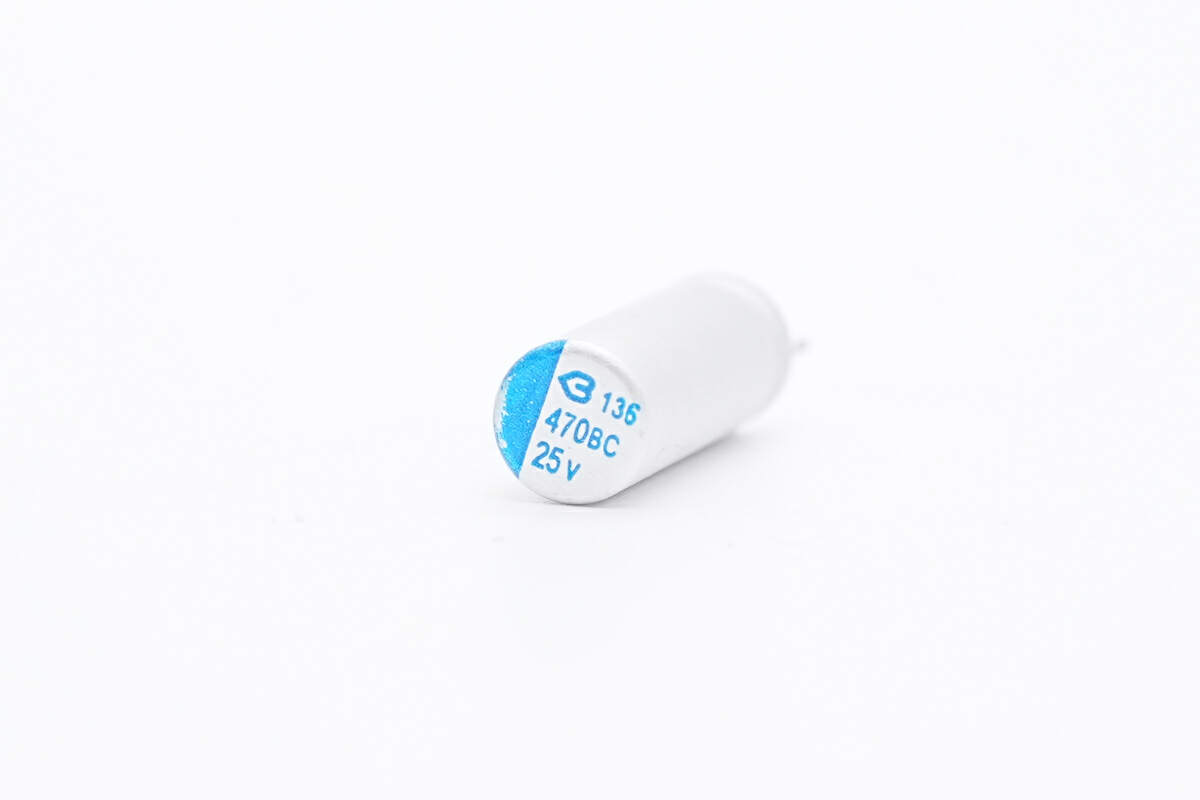
The other solid capacitor for output filtering is also from BERYL electronics. 25V, 470μF.
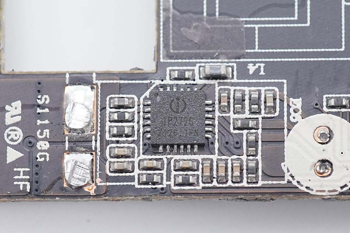
The protocol chip comes from Injoinic IP2726, which integrates multiple protocols, such as PD2.0/3.0, PPS, QC4+, QC2.0/3.0, FCP, AFC, SCP, MTK PE+, Apple2.4A, BC1.2, Samsung 2A and other protocols. It only needs very few external components, which effectively reduces the size and cost.
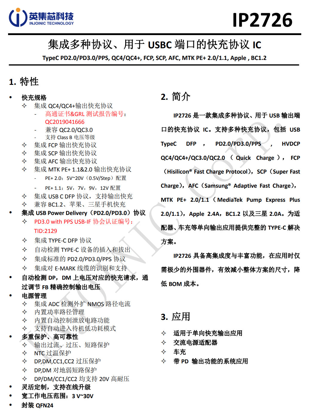
Datasheet of Injoinic IP2726.
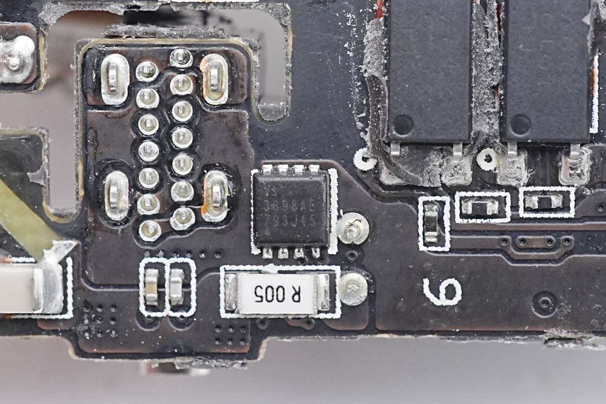
The output VBUS MOSFET is from Vanguard VS3698AE and adopts PDFN3333 package. Withstand voltage is 30V, and resistance is 3mΩ.
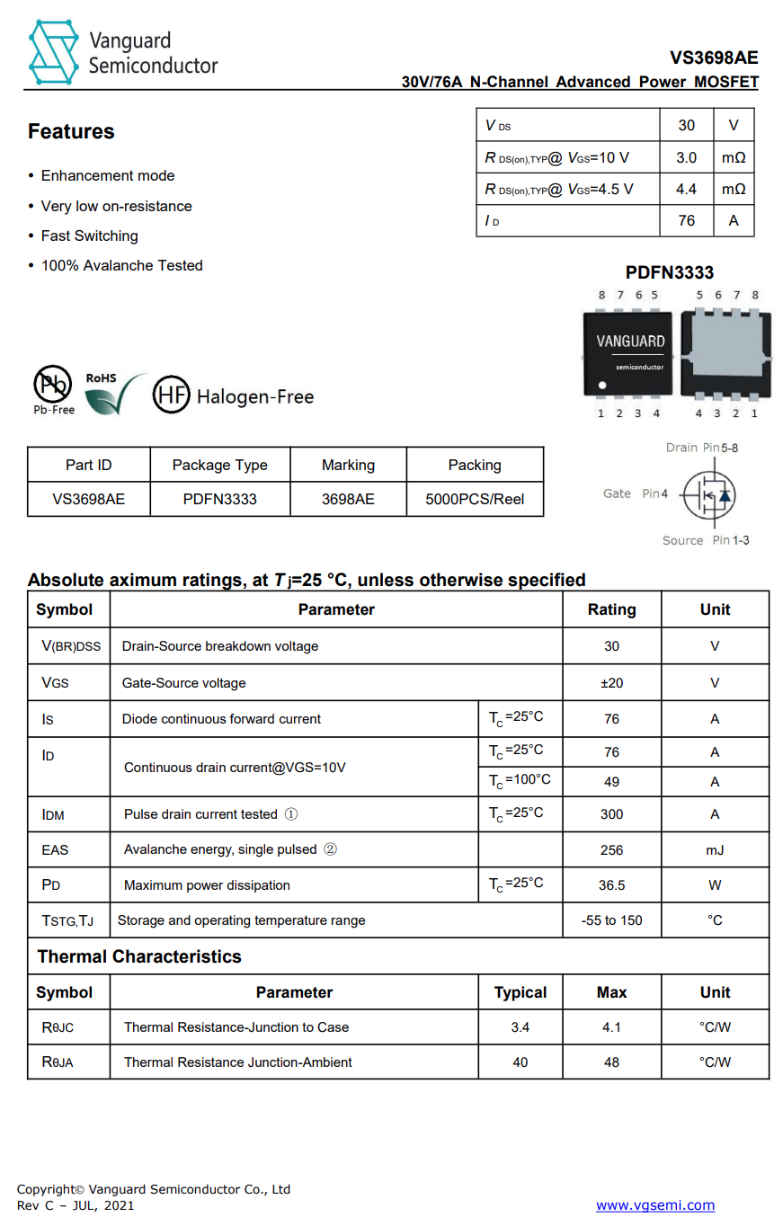
Datasheet of Vanguard VS3698AE.
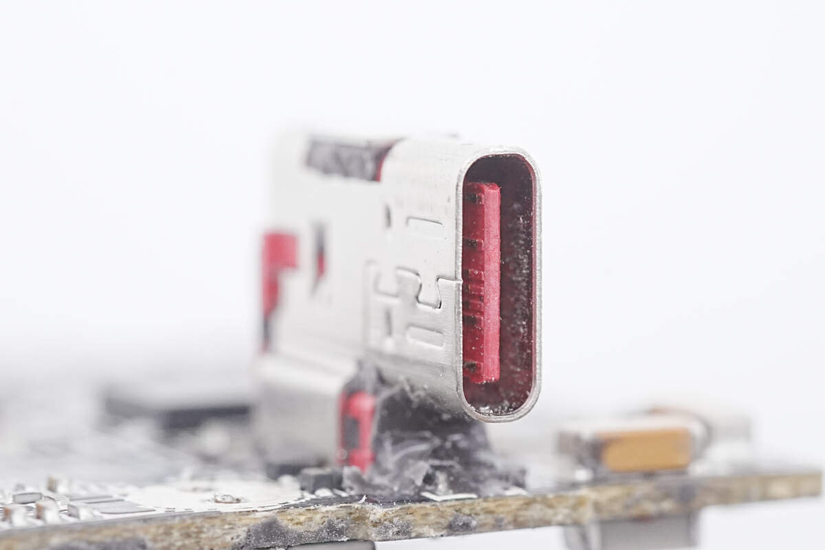
Here is the USB-C receptacle with a red plate inside.
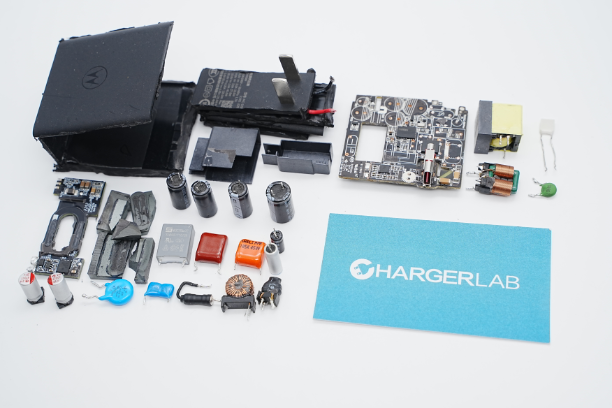
Well, that's all components of this original 125W GaN charger for Motorola MOTO X30 Pro.
Summary of ChargerLAB
This Motorola 125W GaN charger is designed with fixed prongs and black matte shell.
It can support up to 125W when charging MOTO X30 Pro and is compatible with 100W PD fast charging.
We found this charger consists of PFC circuit and QR topology. There're two Navitas GaN power ICs inside. Model is NV6134. One of them is used for the PFC boost circuit, and the other one is used for the QR topology of the switching power supply. The PFC boost controller is from Silergy, and the synchronous rectifier and VBUS MOSFET are from Vergiga. The protocol chip is from Injoinic IP2726.
The entire module is covered with silicone adhesives, and the graphite thermal sheet can enhance heat dissipation performance. The internal module is very compact, and the planar transformer can greatly reduce the thickness. And the built-in thermal fuse can be used for the overheating protection of this charger.
Related Articles:
1. Teardown of Motorola Original 125W GaN Charger for edge 30 ultra (MC-1258)
2. Teardown of Brand New Apple 140W USB-C GaN Charger
3. Teardown of New Samsung 45W GaN Charger EP-T4510 (For Samsung S22 Series)

