Introduction
SUPERVOOC charging technology from OnePlus is considered one of the fastest and most efficient charging technologies currently available, allowing you to quickly charge your device and get back to using it in no time. So today, let's take a look at the components and structure from the OnePlus SUPERVOOC 100W dual ports charger.
Product Appearance
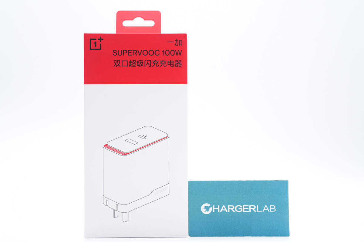
OnePlus SUPERVOOC 100W dual ports charger has a simple and stylish appearance with a red and white color scheme, and the front of the package features the OnePlus name, logo, charger appearance.
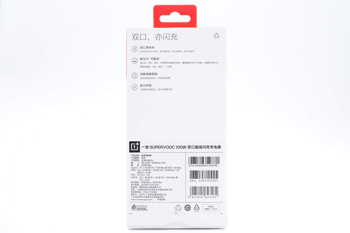
The major selling points are on the back.
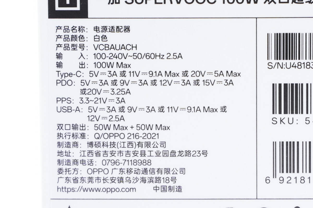
And the detailed information about the product, including product name, color, model, input and output parameters, interface type, manufacturer, and other information are on the bottom.
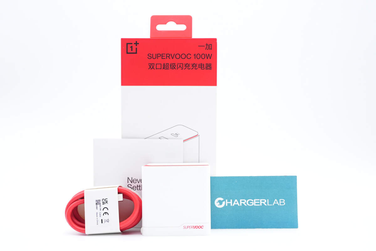
The packaging includes the OnePlus SUPERVOOC 100W dual ports charger, cable, user manual.
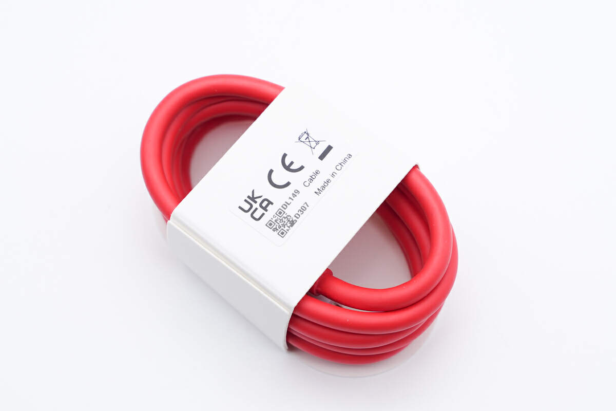
The cable is red and passed CE certified.
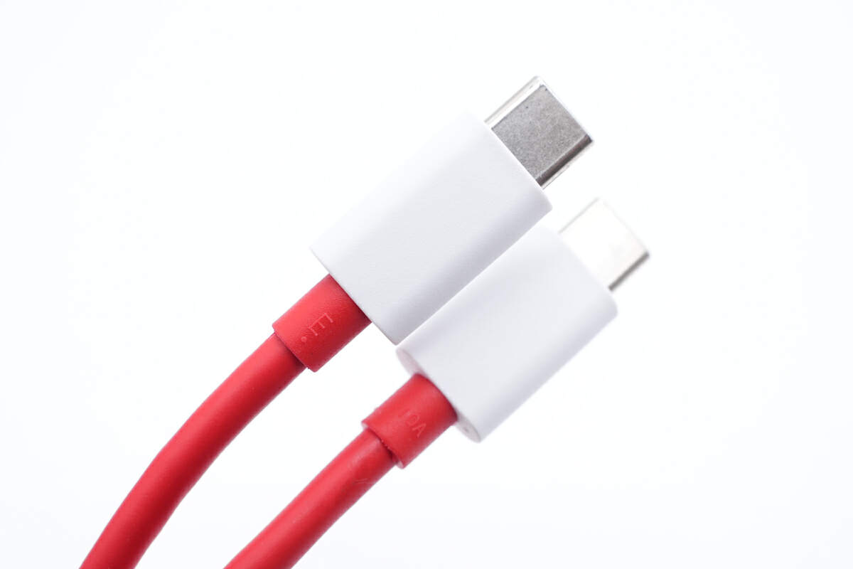
It's also a 10A high-current fast-charging dual USB-C cable.
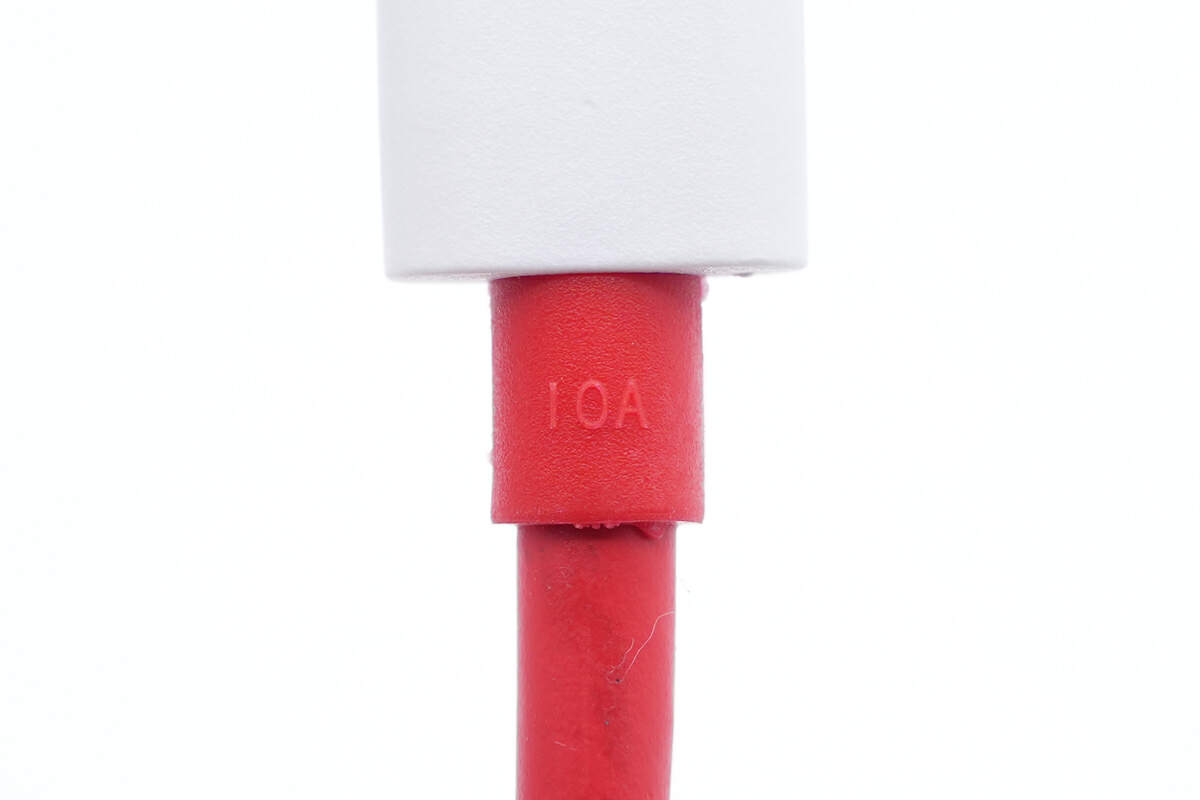
The "10A" can be seen here.
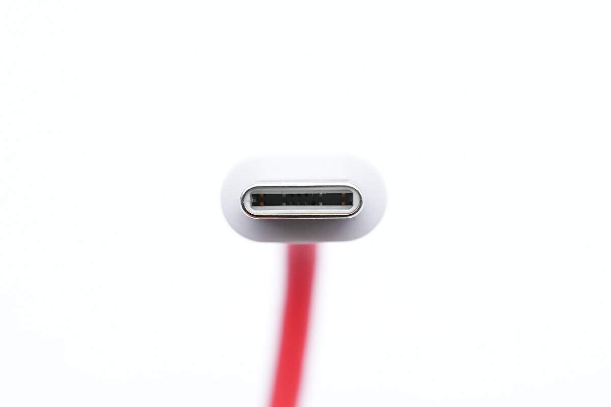
The USB-C connector has a non-full PIN design and is white on the inside.
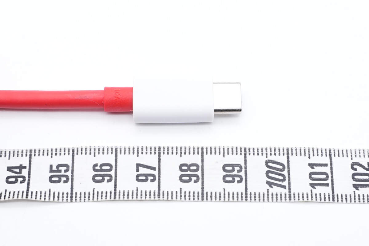
The cable length is about 1m (3 ‘3.37”).
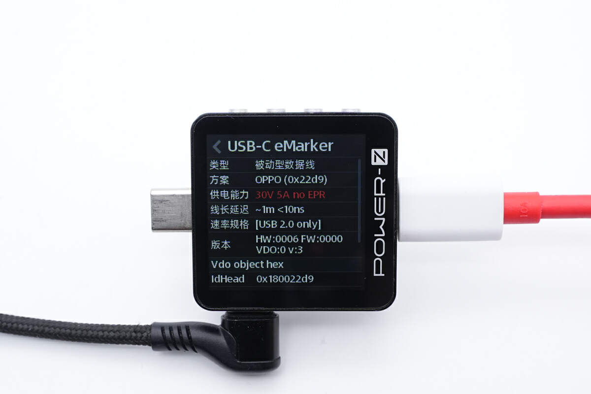
The ChargerLAB POWER-Z KM003C shows it's a USB 2.0 cable with built-in E-Marker chip.
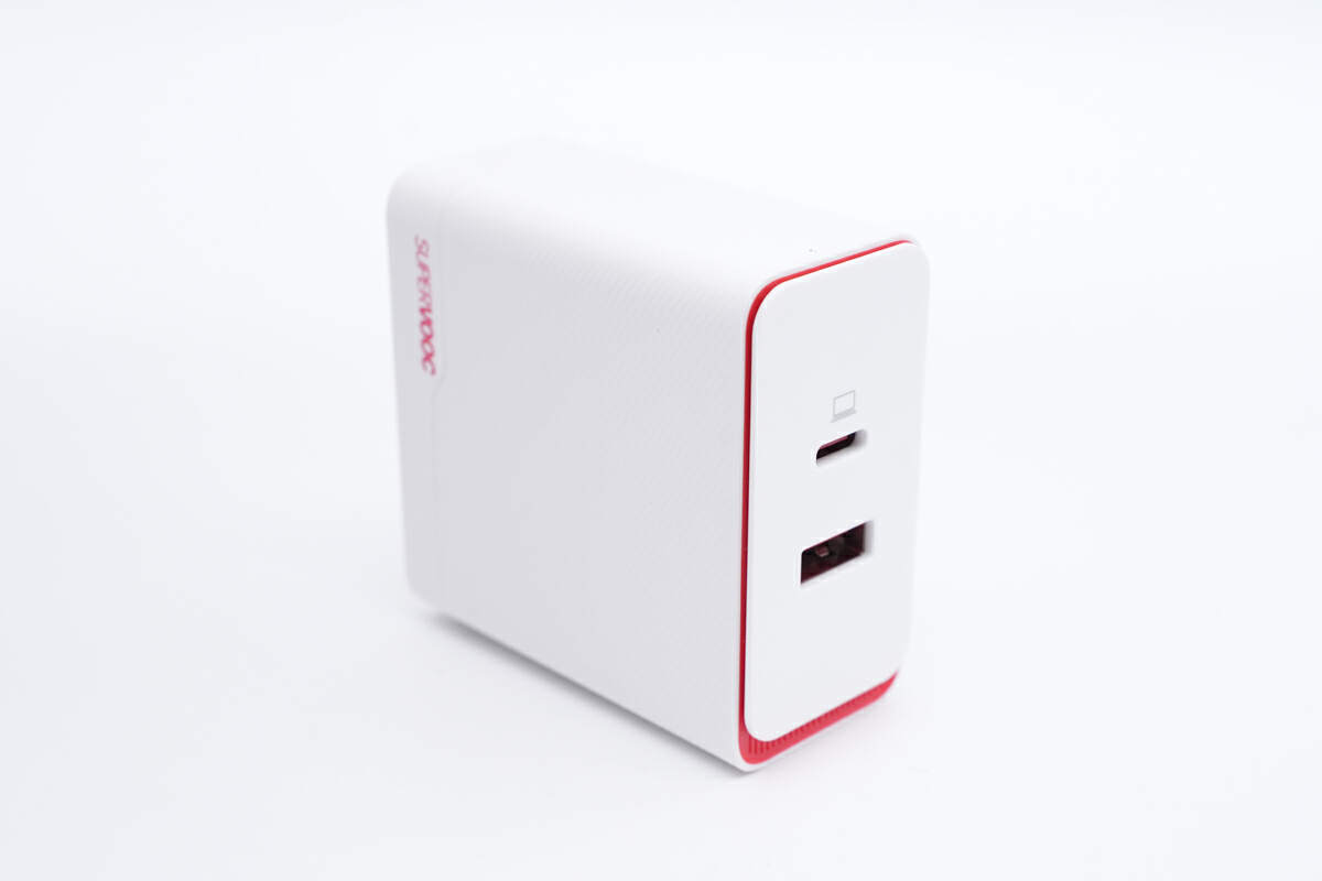
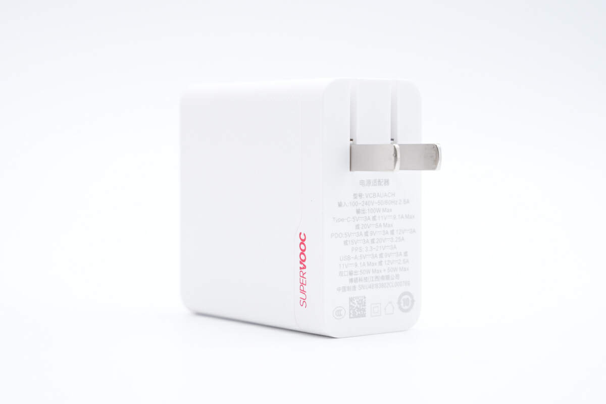
The front of the shell is printed with "SUPERVOOC", and the overall appearance is modern and stylish.

The surface of the shell is covered with shallow striped grooves, which can facilitate the user to hold it more tightly.
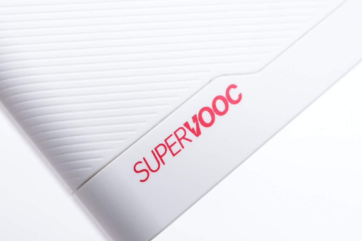
The red SUPERVOOC logo is at the corner.
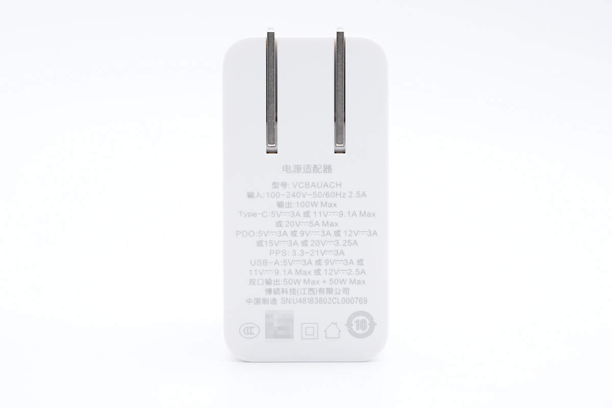
All specs info are printed on the input end.
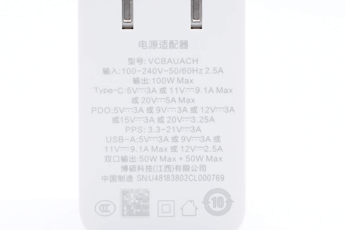
Model is VCBAUACH. It can support input of 100-240V~50/60Hz 2.5A. The single output can be up to 100W, and the dual output power can be divided into 50W and 50W.
The input prongs can be folded even for such a small charger.
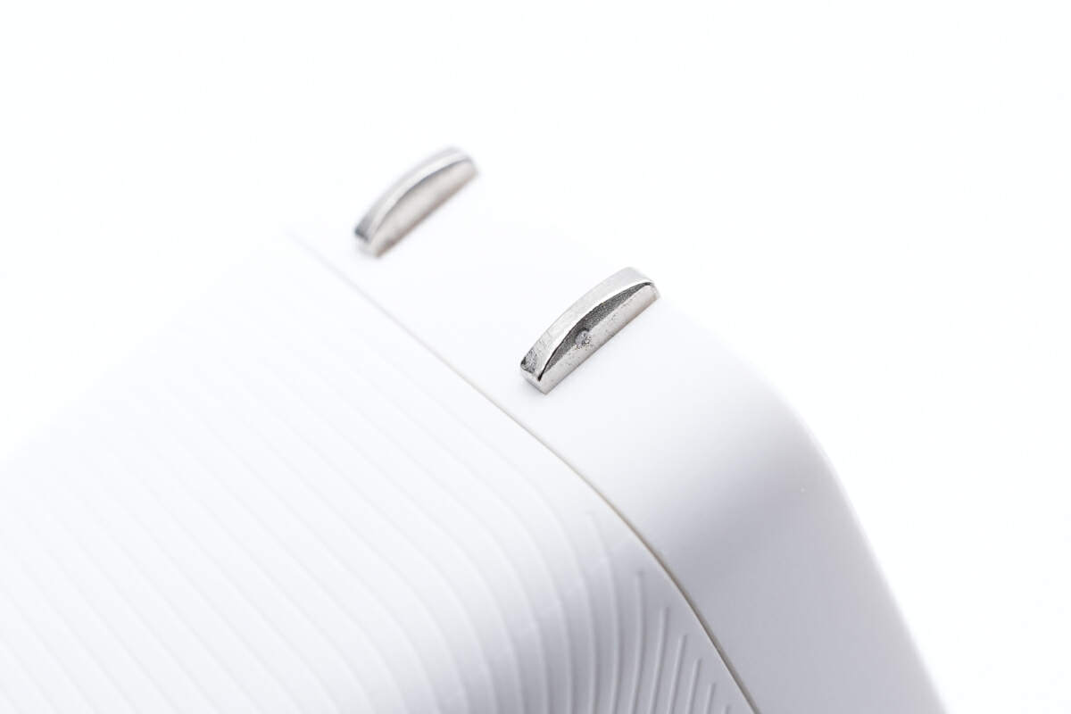
The prongs are slightly protruding for easy use.
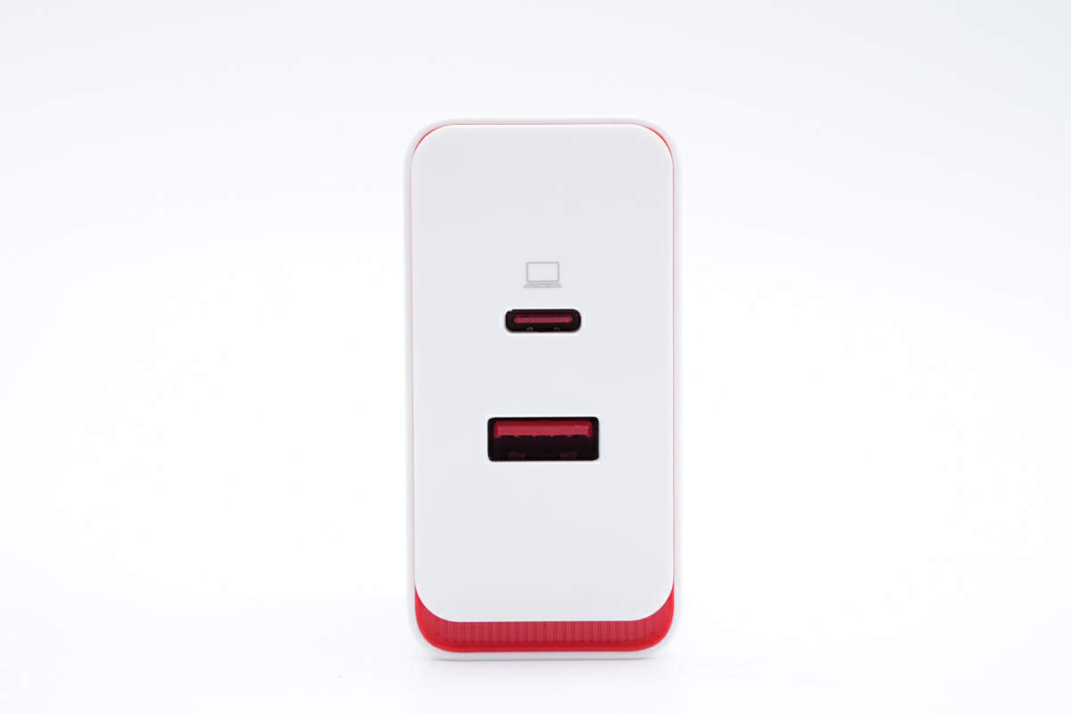
A USB-A and a USB-C are on the output panel, which still adopt white and red design.
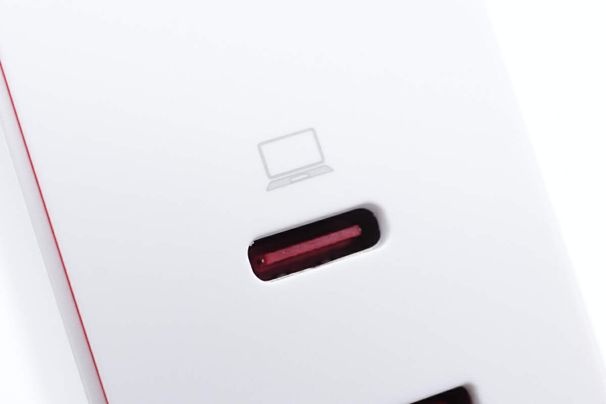
And there is a littcle computer icon on the top of the USB-C port.
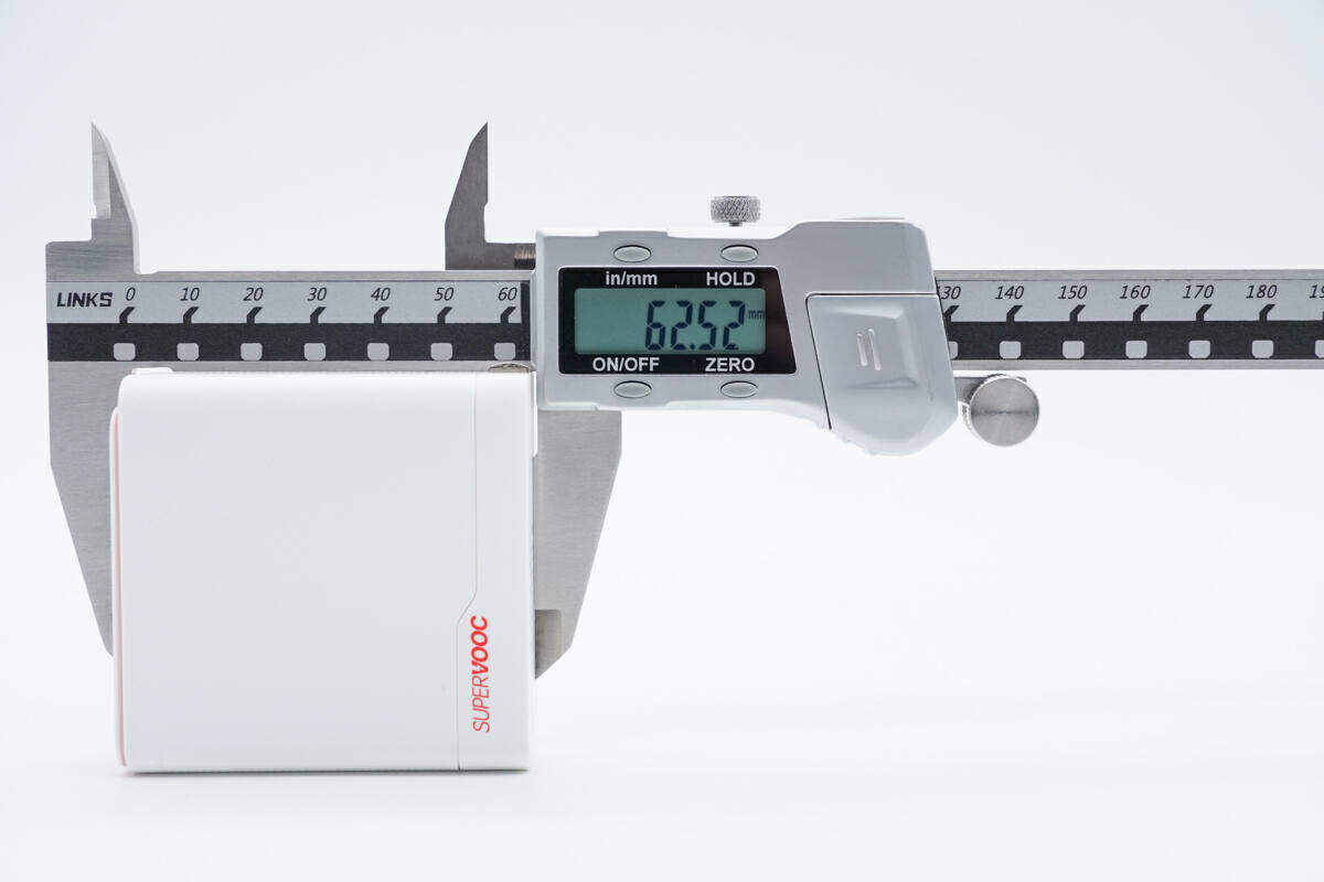
The length of the charger is about 62.5mm (2.46 inches).
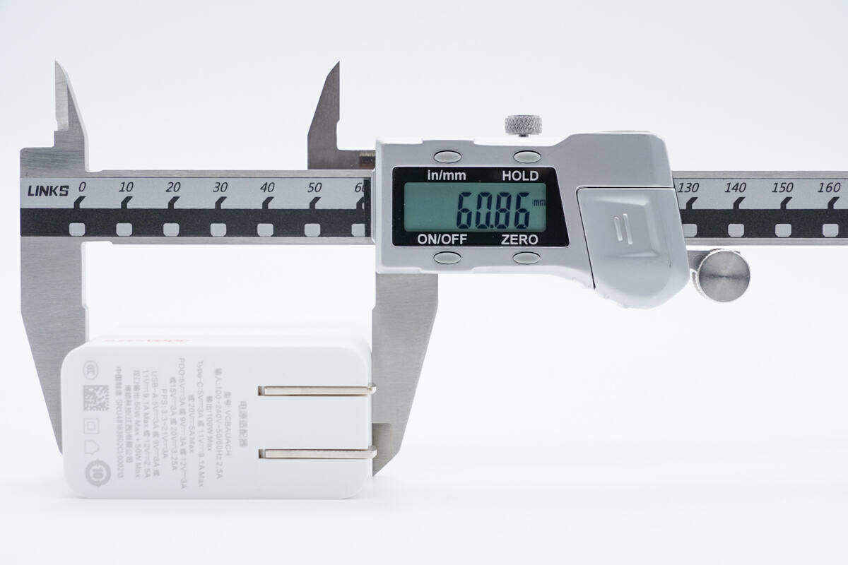
The width is about 61mm (2.40 inches).
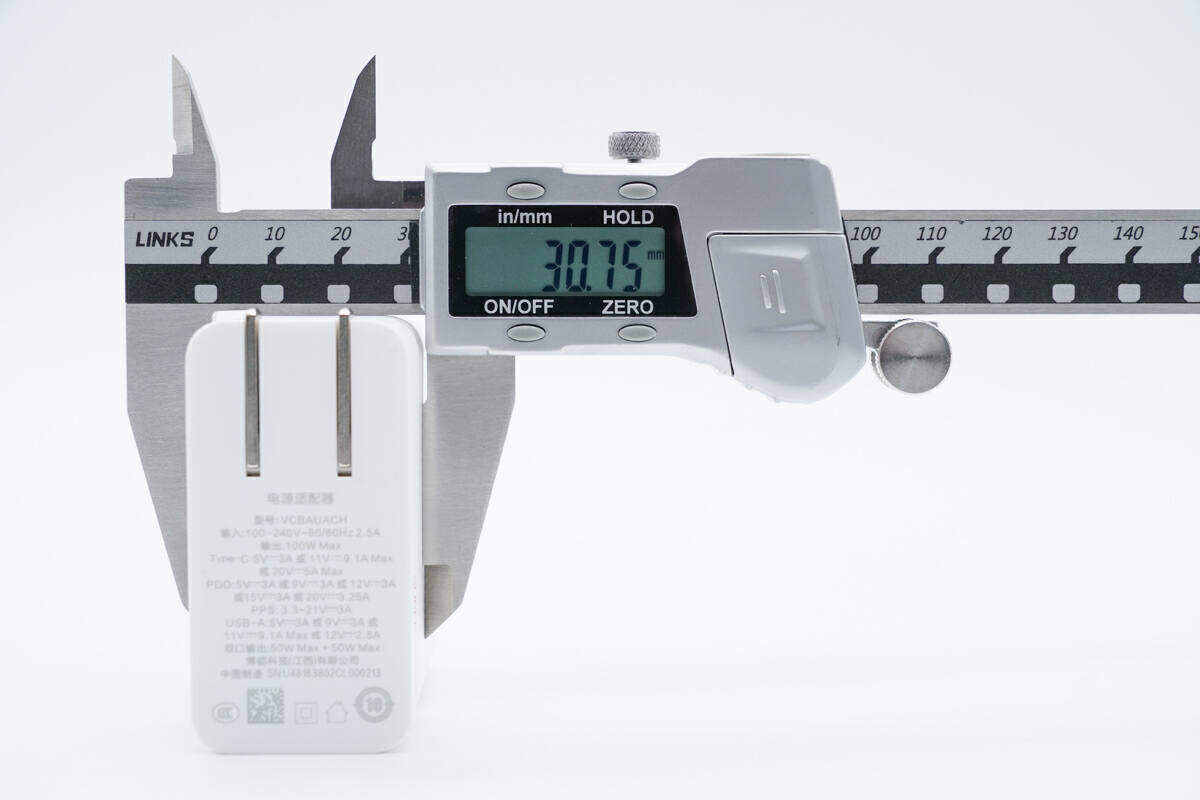
And the height is about 31mm (1.22 inches).
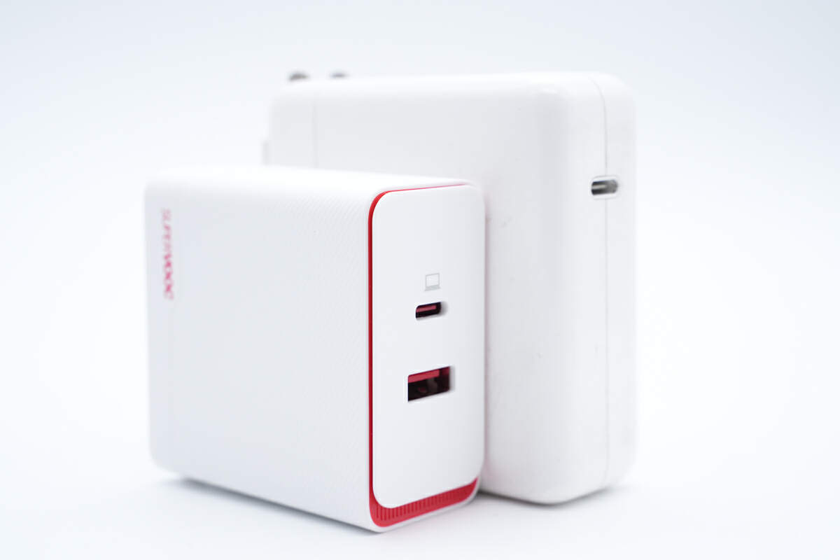
Compared with the Apple 96W charger, the size is much smaller but has one more port.
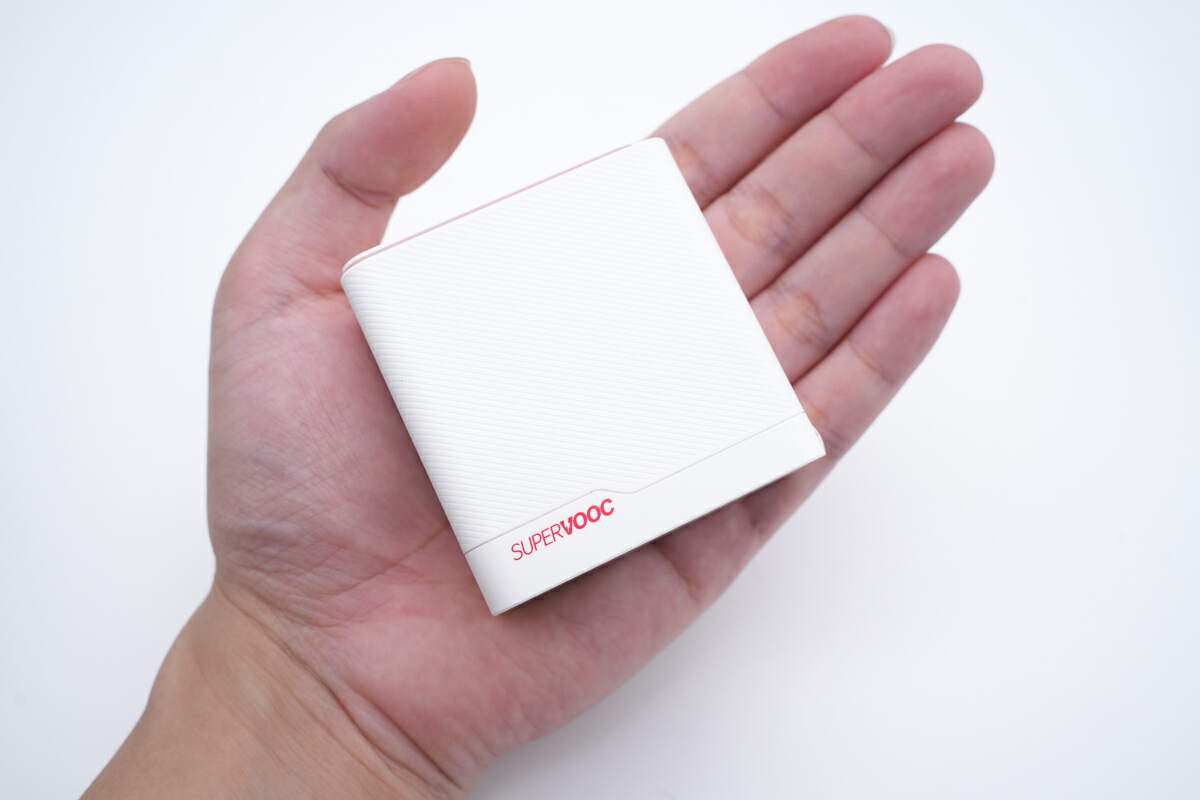
This is how it looks like on my hand.
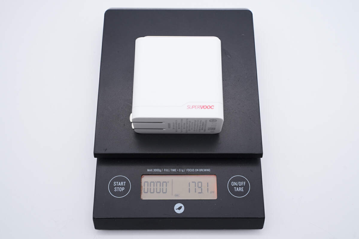
And the weight of the charger is about 178.5g (6.3 oz).
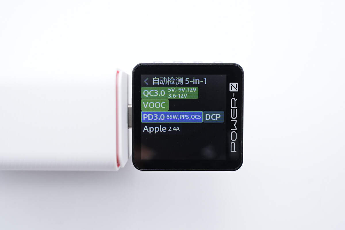
The ChargerLAB POWER-Z KM003C shows the USB-C can support QC3.0, VOOC, PD3.0, PPS, Apple 2.4A, DCP protocols.
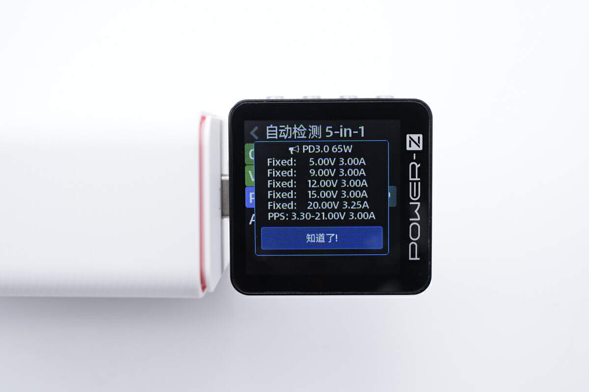
And it has five fixed PDOs of 5V3A, 9V3A, 12V3A, 15V3A, 20V3.25A, and a set of PPS, which means it can support 65W PD protocol.
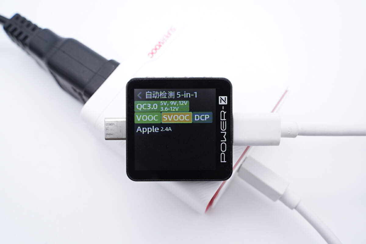
And the USB-A can support QC3.0, VOOC, SVOOC, Apple 2.4A, and DCP protocols.
Teardown
Next, we took apart the charger from the input side.
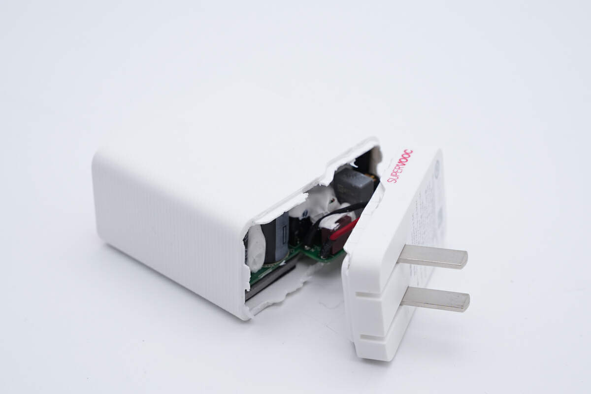
Pry along the gap to open it up, the internal PCBA module is fixed by adhesives and cannot be taken out.
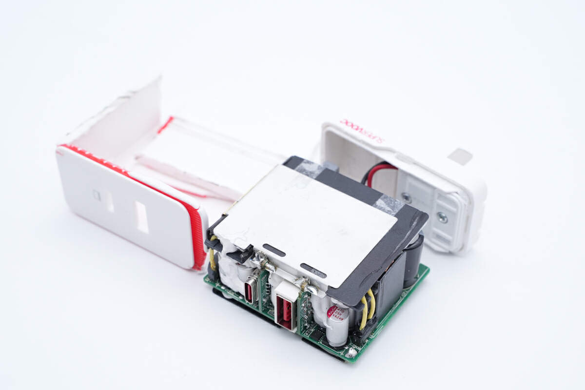
Then, use the cutting machine to cut off the plastic shell and take it out.
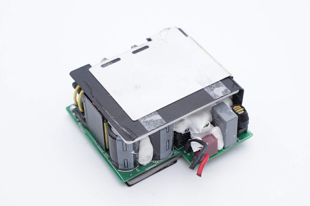
The PCBA module is connected by wires, and the components are fixed with adhesives.
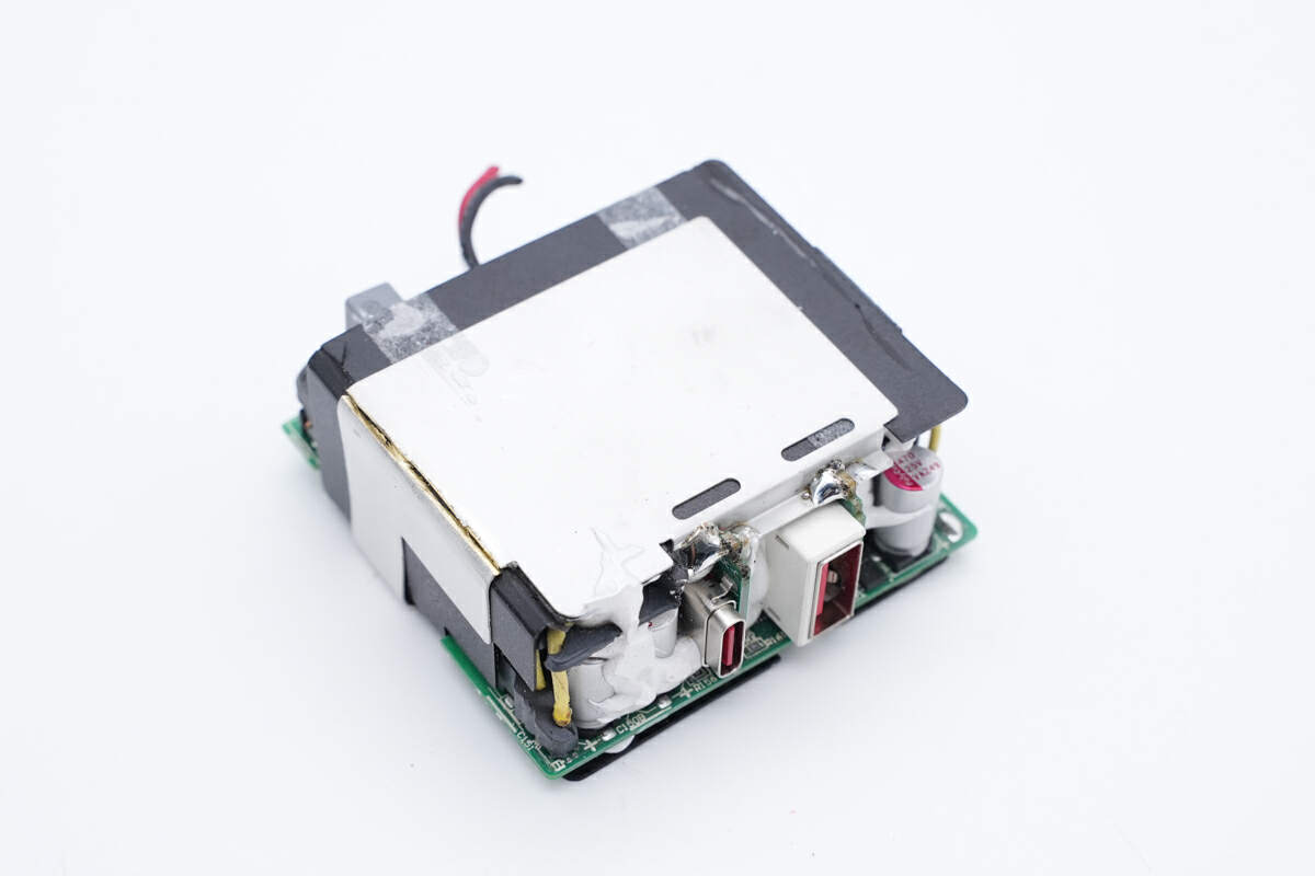
The gaps between different components are filled with silicone adhesives for fixing and heat dissipation.
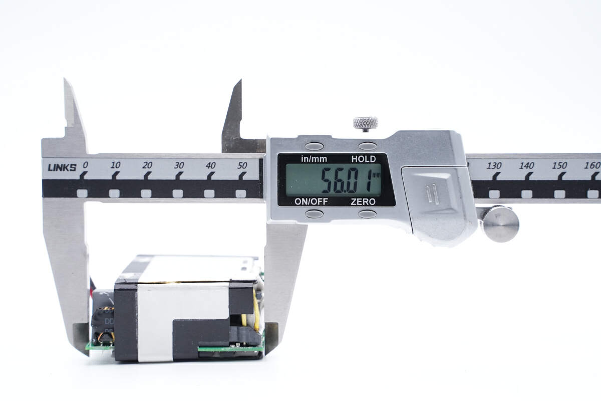
The length of the PCBA is about 56mm (2.20 inches).
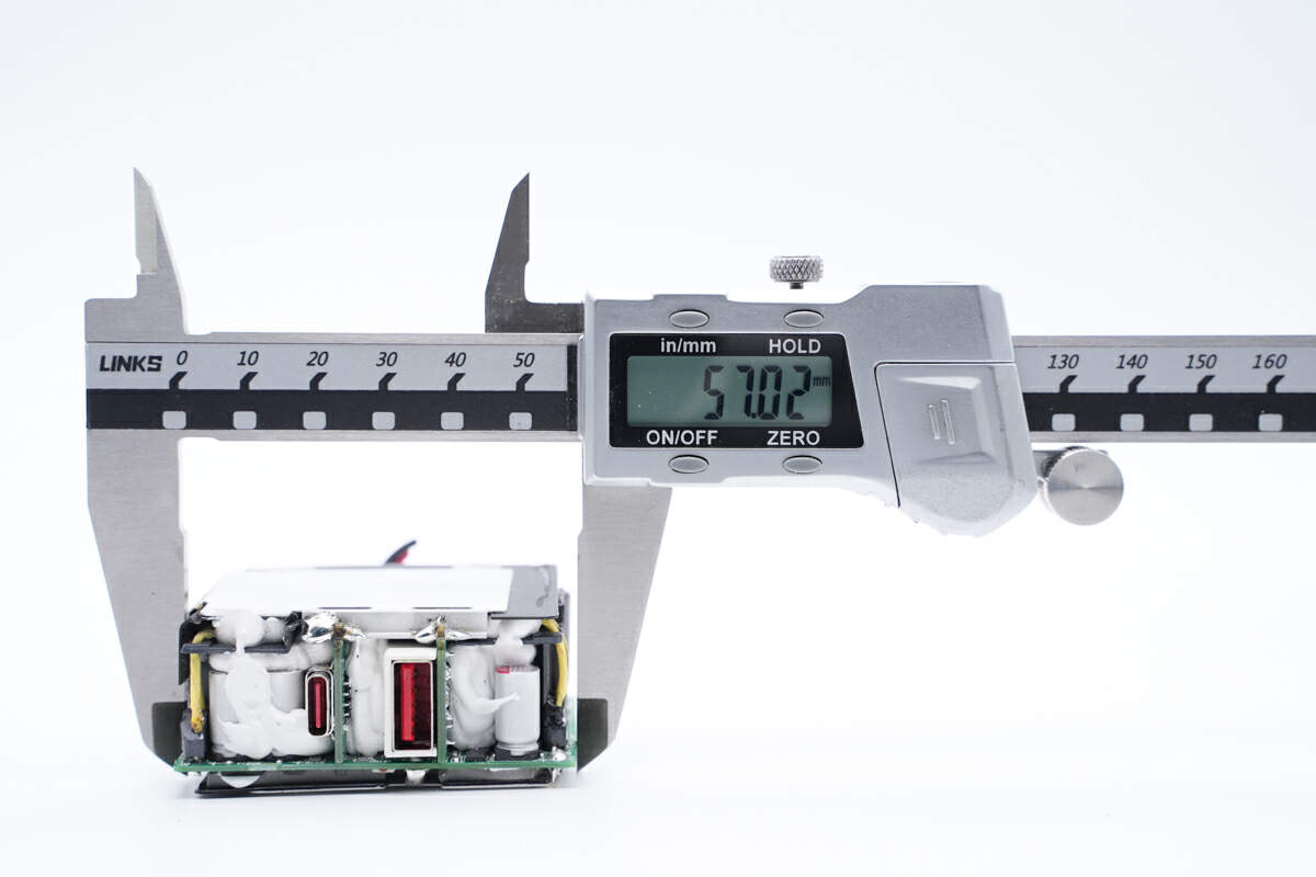
The width is about 57mm (2.24 inches).
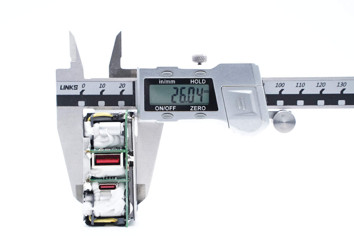
And the height is about 33mm (1.02 inches).
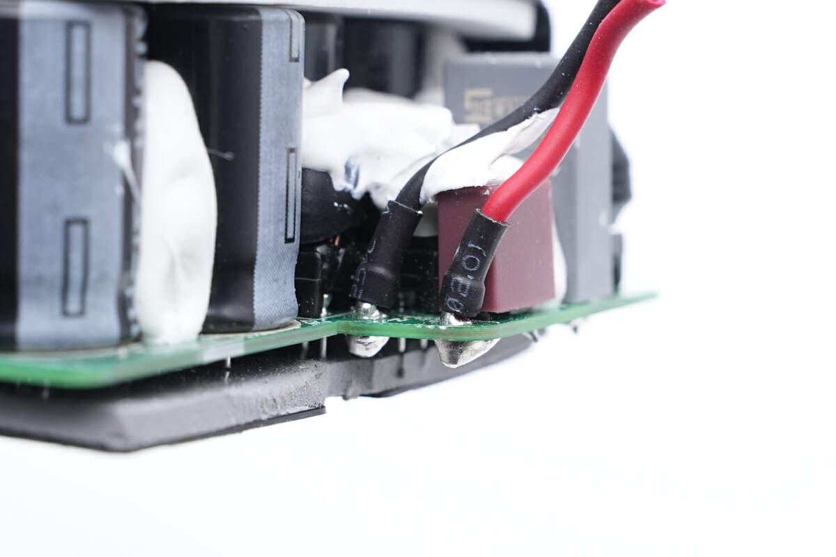
The power input wires are insulated with heat shrink tubing
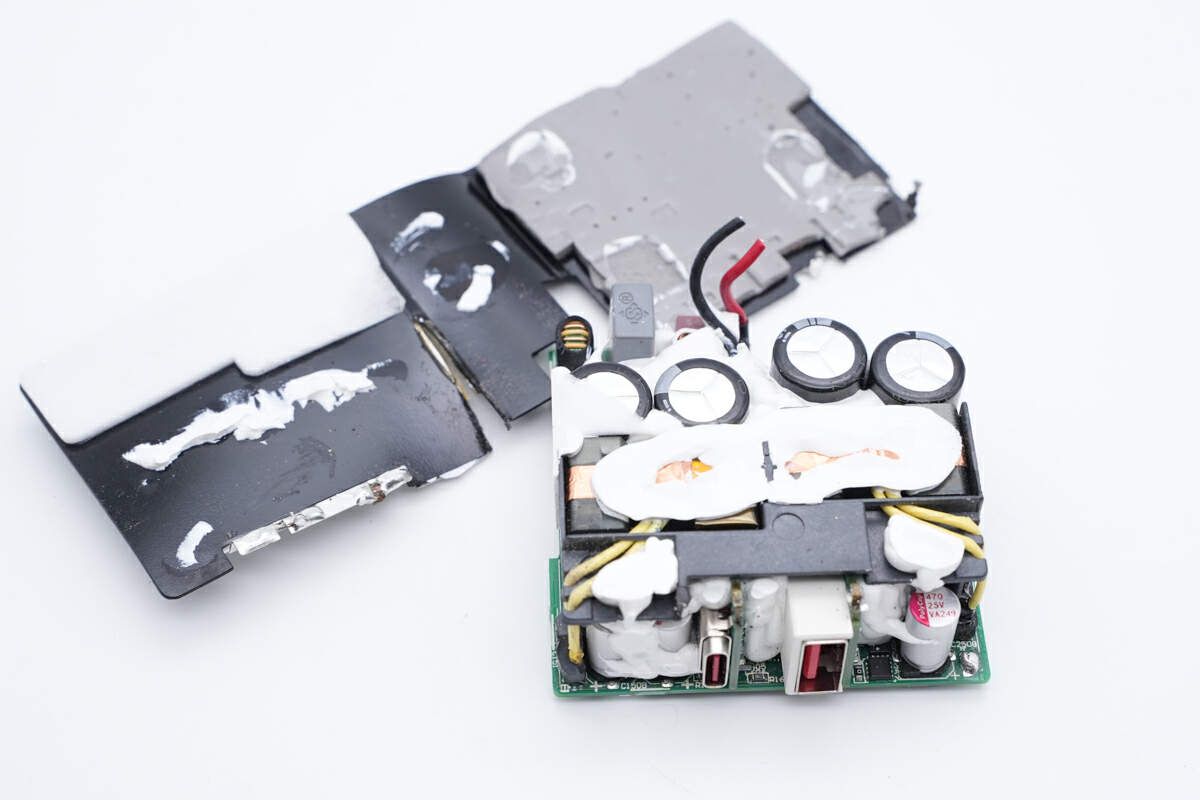
Remove the heat sink covering the PCBA module. There is a thermal pad on the back of the PCBA module to dissipate heat for the bridge rectifier and the master control chip. The transformer dissipates heat through the heat sink, and foam is pasted at the position of the electrolytic capacitor.
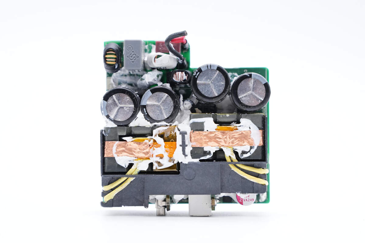
The input fuse, common mode choke, safety X2 capacitor, filter capacitor and transformer are on the front of PCBA.
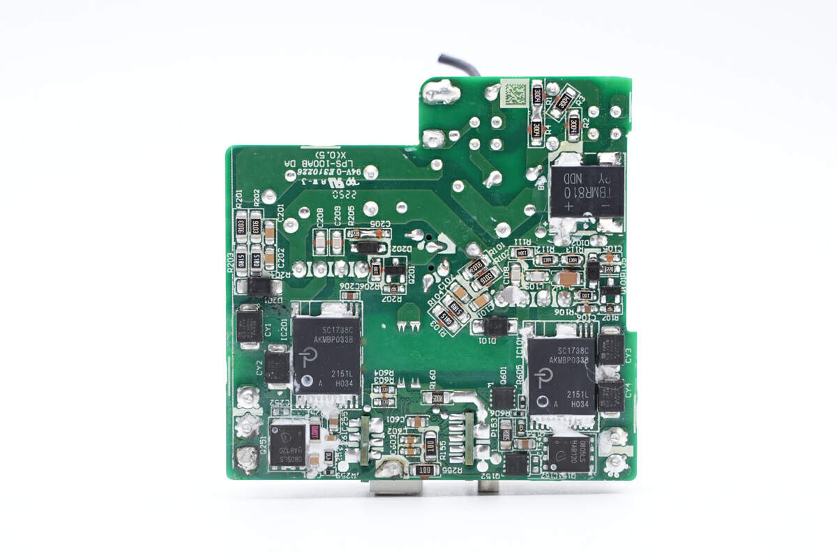
The bridge rectifier, two PI master control chips, SMD Y capacitors and synchronous rectifiers are on the back. Due to the use of PI's highly integrated master control chip, the charger circuit is quite streamlined.
The charger is equipped with two independent and symmetrical QR switching power supplies, allowing for a wide range of voltage output. The charger's output voltage is controlled by a protocol chip, which enables two ports to charge independently at 50W each. In instances where only one port is connected to a device, the protocol chip will automatically combine the two outputs to provide a single high-power output of 100W. Next, let's introduce every single component.
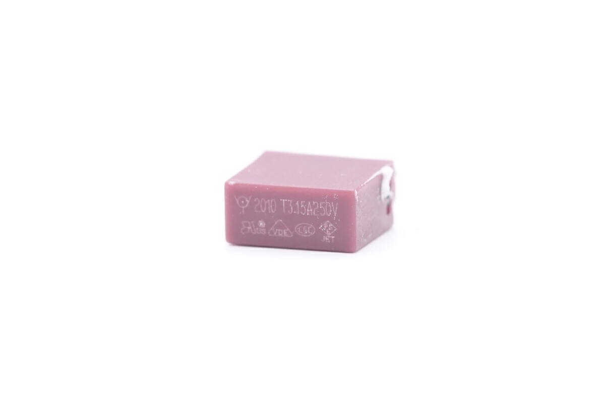
The input fuse is from WalterFuse. 3.15A 250V.
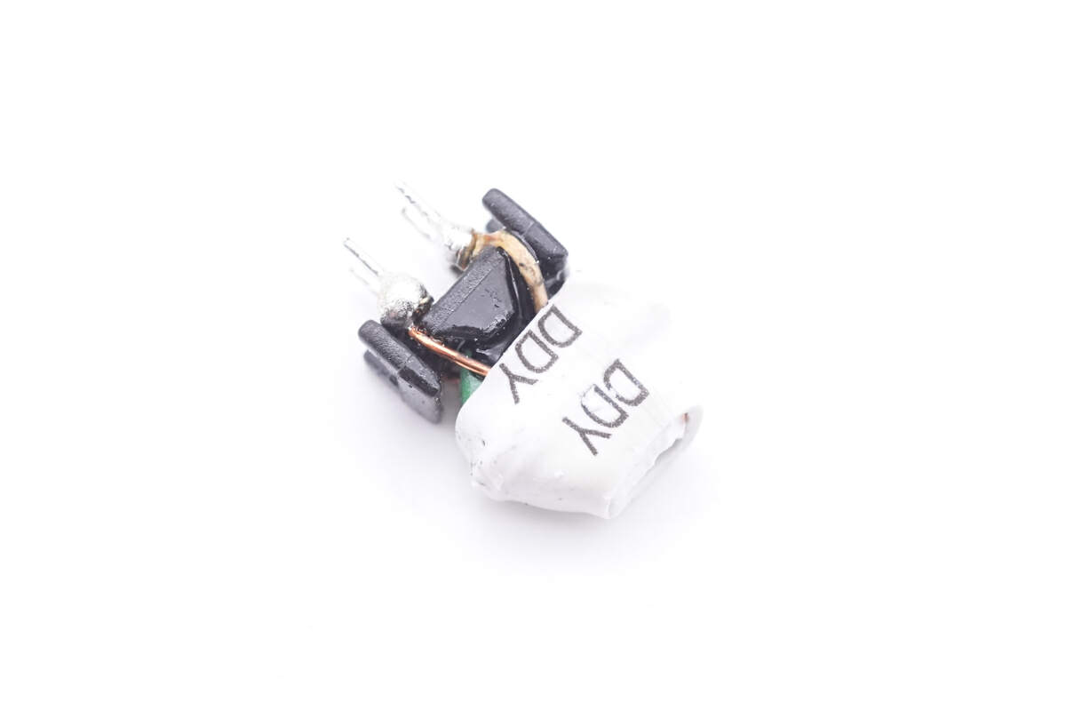
The first common mode choke is insulated with a white heat-shrinkable tubing.
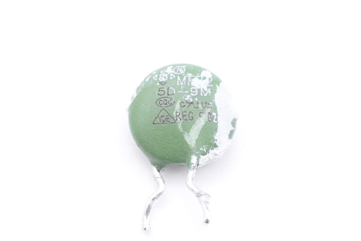
The green NTC thermistor is from STE, used to suppress the inrush current when the charger is plugged in. Model is 5D-9M.
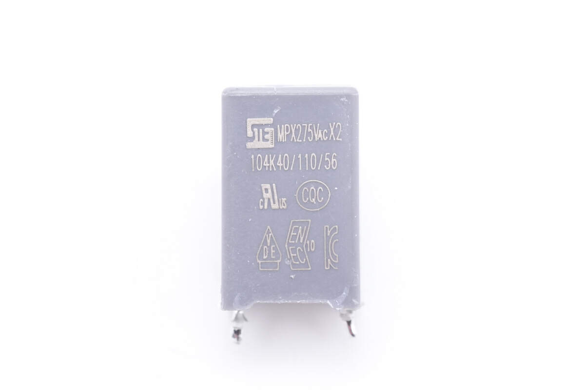
The safety X2 capacitor is also from STE. 0.1μF.
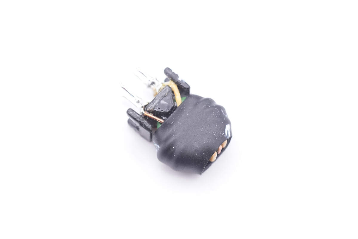
The second common mode choke is insulated with a black heat-shrinkable tubing.
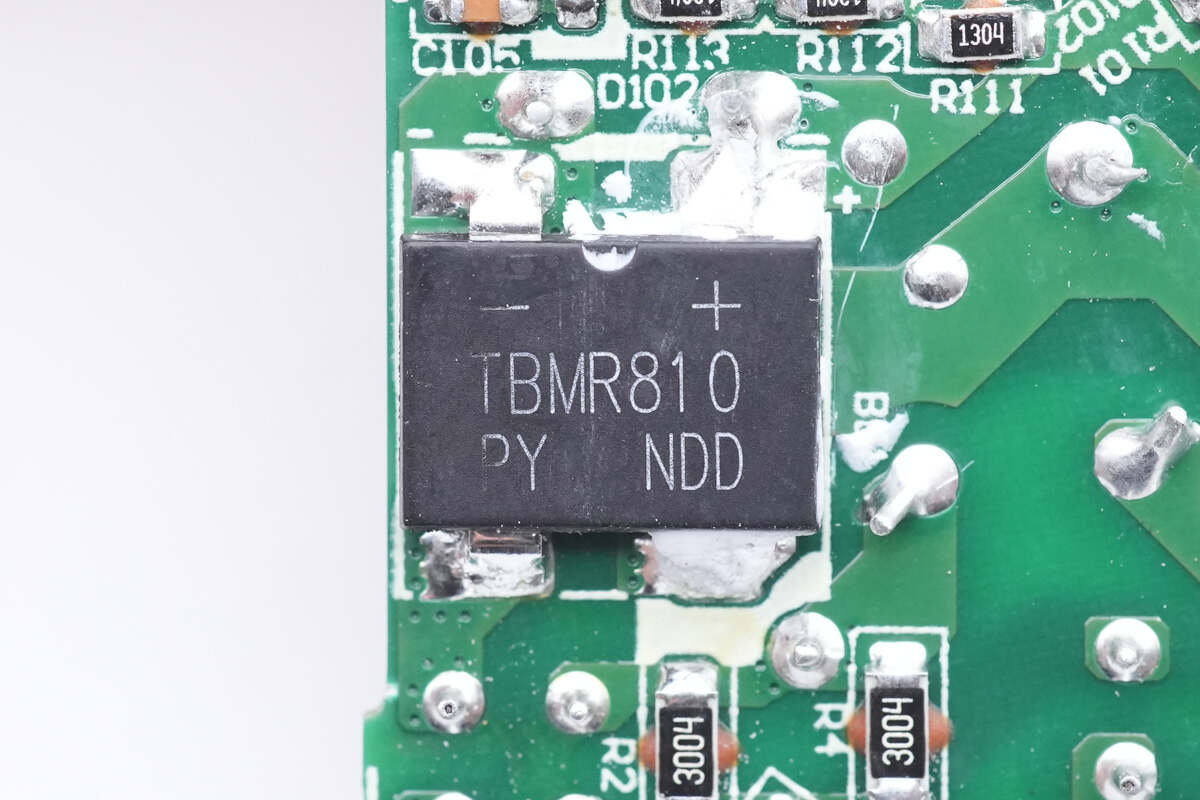
The bridge rectifier is from Pingwei, model is MR810, and the thermal pad and silicone adhesive can enhance its heat dissipation performance. 8A 1000V.
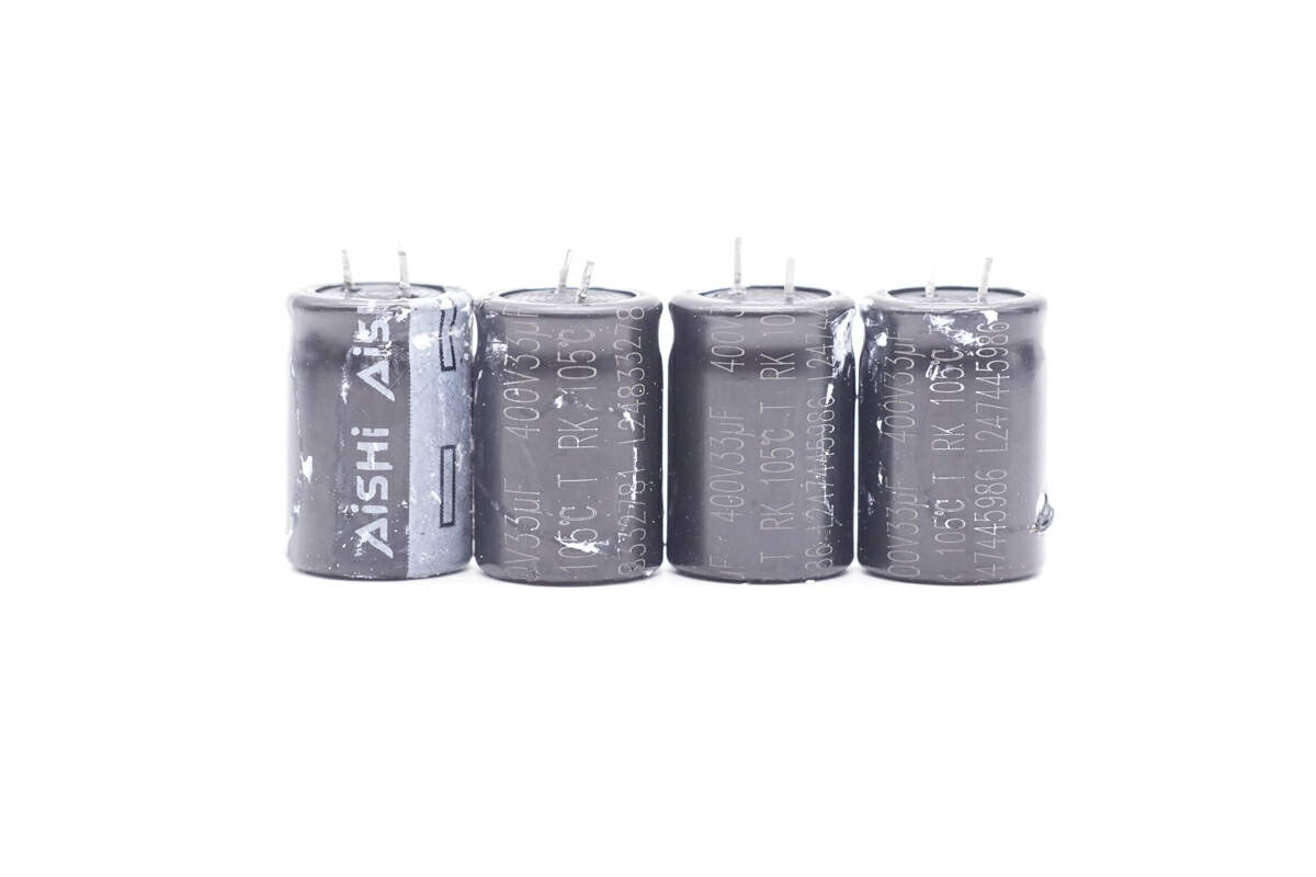
And those four electrolytic capacitors are connected in parallel for input filtering and are from AiSHi RK series. 400V 33μF for each.
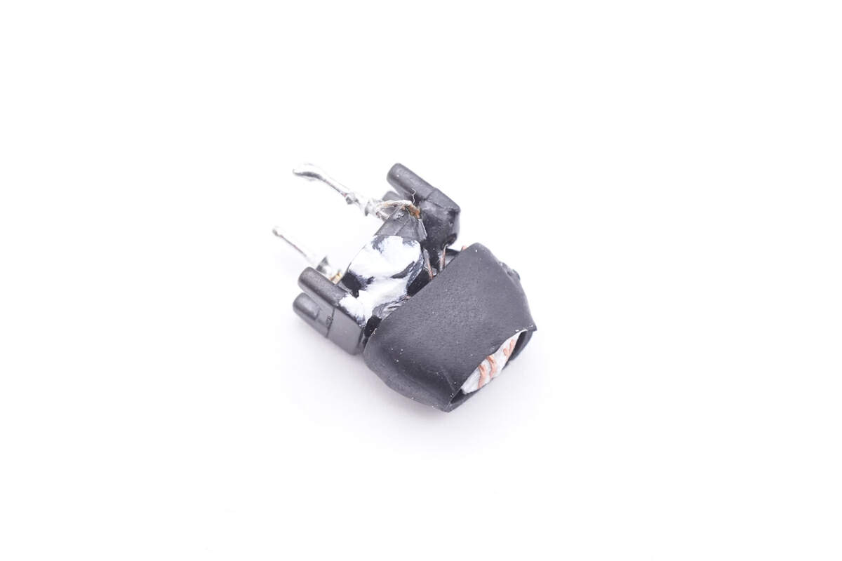
The differential mode choke is wrapped with heat-shrinkable tubing.
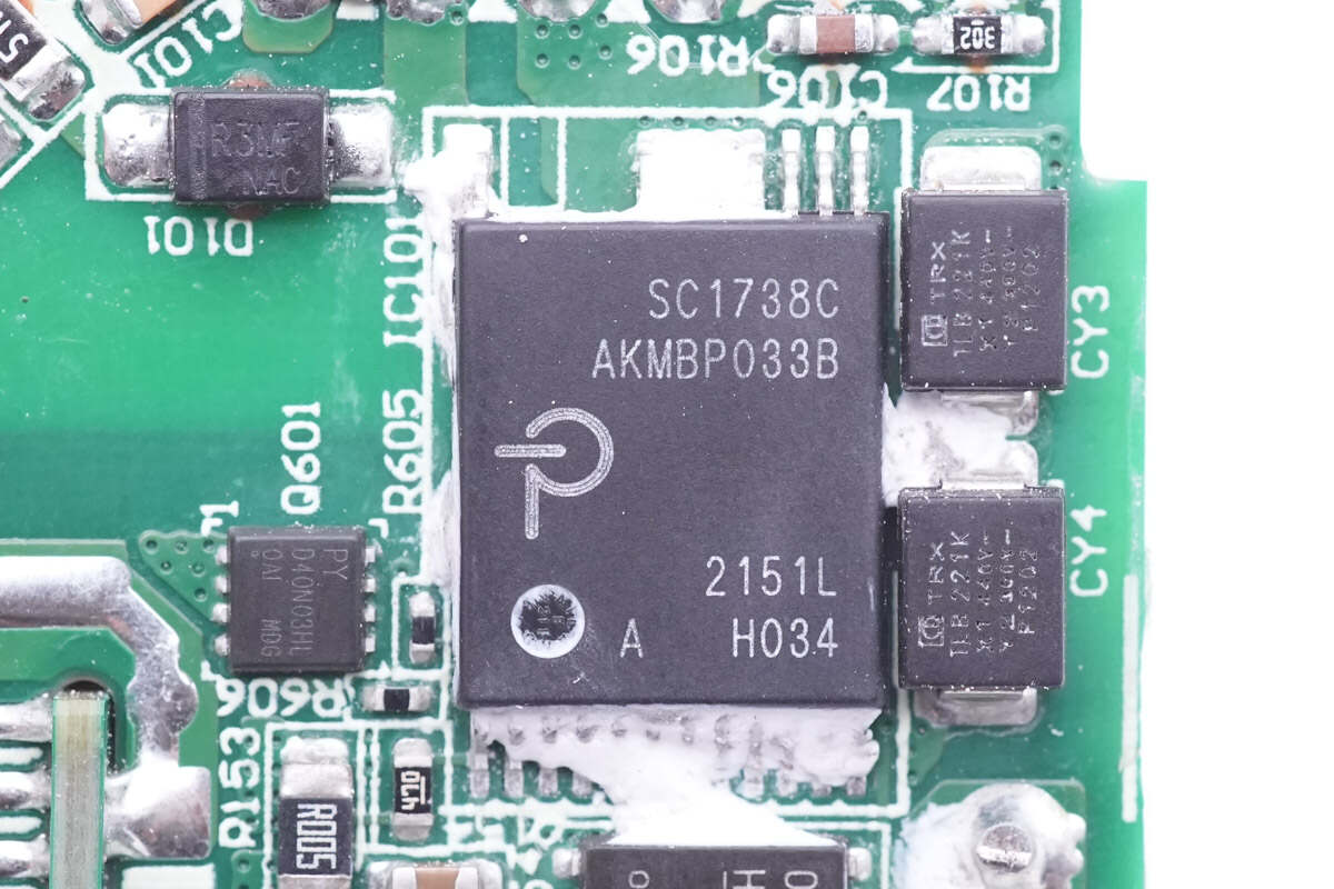
The master control chip utilized in this charger is the PI SC1738C, a custom-made model that could be interpreted as a high-powered adaptation of the InnoSwitch3-Pro power chip. It combines high-voltage switching, synchronous rectification, and FluxLink feedback functions into one digitally controlled cv/cc offline QR flyback switching IC. Specifically designed for use in efficient USB PD 3.0+PPS/QC adapters, it also supports the broader application of wide-voltage 50W adapters.
The SC1738C communicates with the protocol chip through the I2C interface and can dynamically adjust the output voltage and current. All protection functions can be configured.
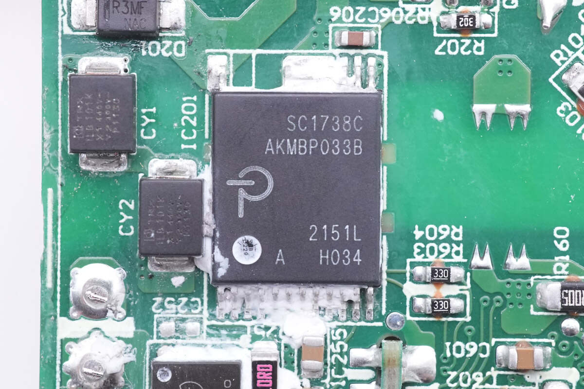
Here is another SC1738C.
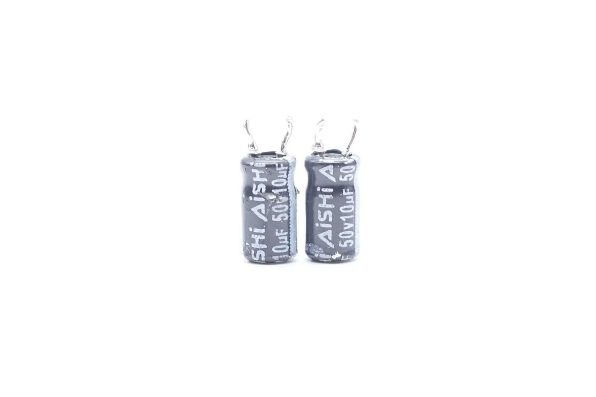
The two tiny electrolytic capacitors can power two master control chips. 50V 10μF for each.
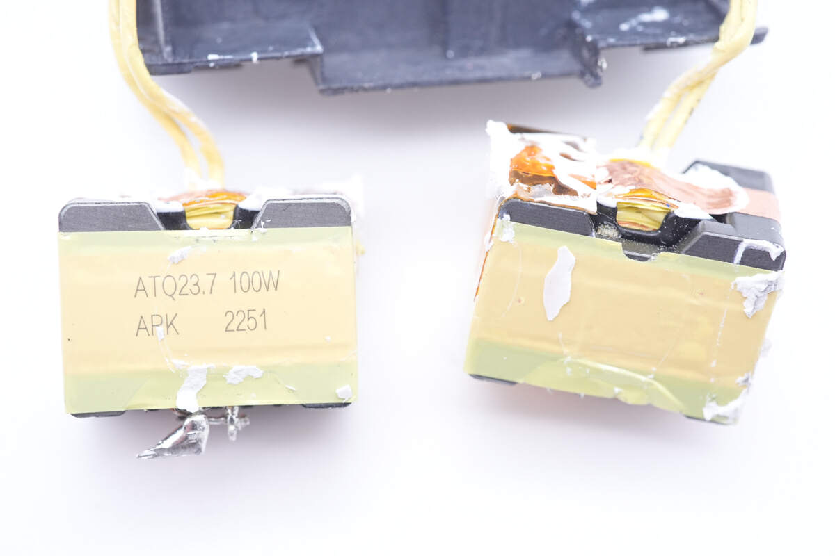
The two transformers are insulated with yellow tape, and the ferrite core is ATQ23.7, wrapped with copper foil for shielding.
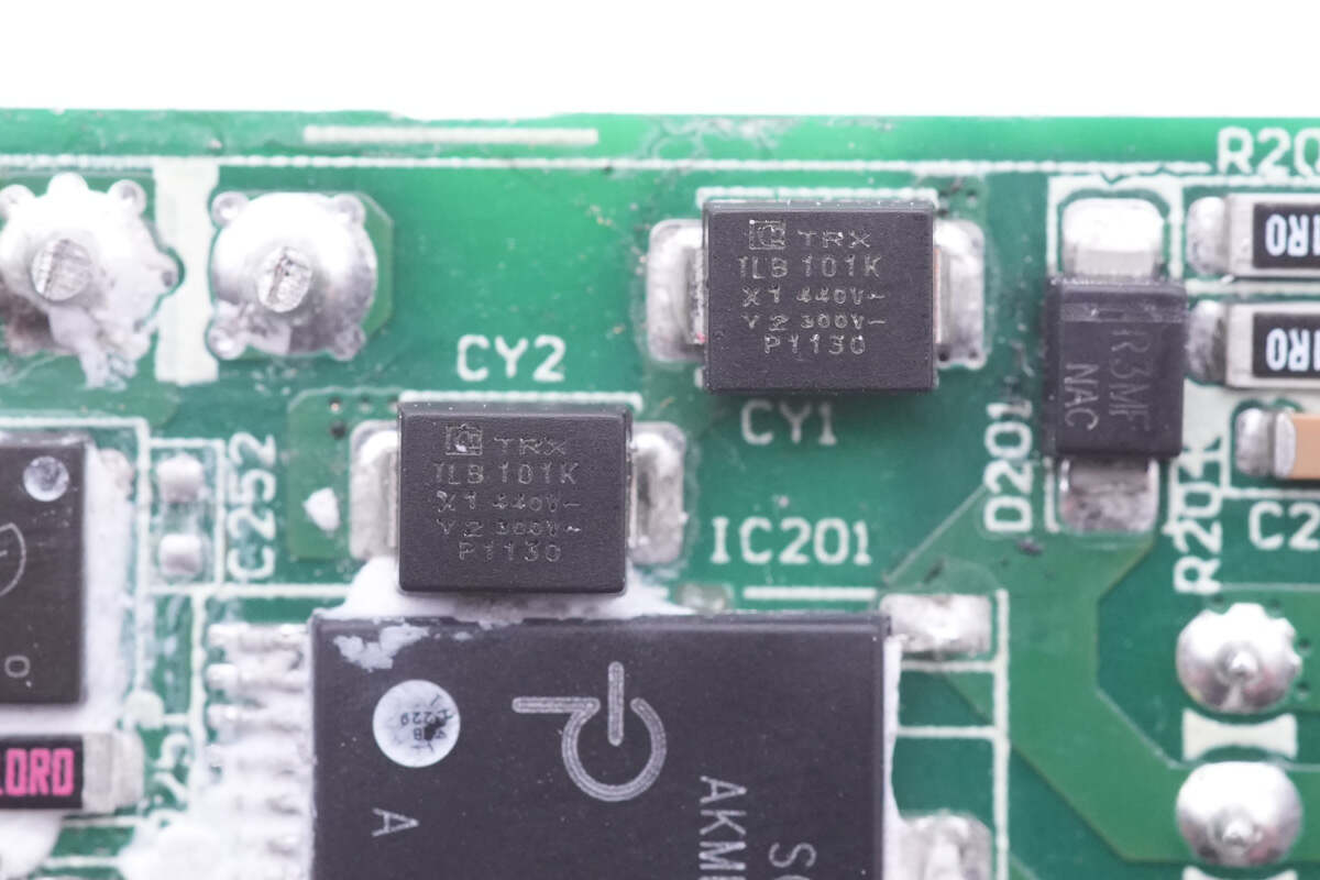
The charger utilizes SMD Y capacitors from the TRX SMD-Y2 series, specifically the TBY2101KB model. To enhance voltage resistance and increase safety ratings, two capacitors are connected in series, satisfying regulatory standards. TRX's SMD Y capacitors features in small size and light weight, and are very suitable for high-density power supply products such as GaN charger.
TRX focuses on the R&D, production and sales of passive components, with a registered capital of 100 million yuan. It has two types of capacitor brands: SMD TRX and DIP TY capacitors. TRX will devote itself to the research of ceramic materials in order to provide customers with more solutions.
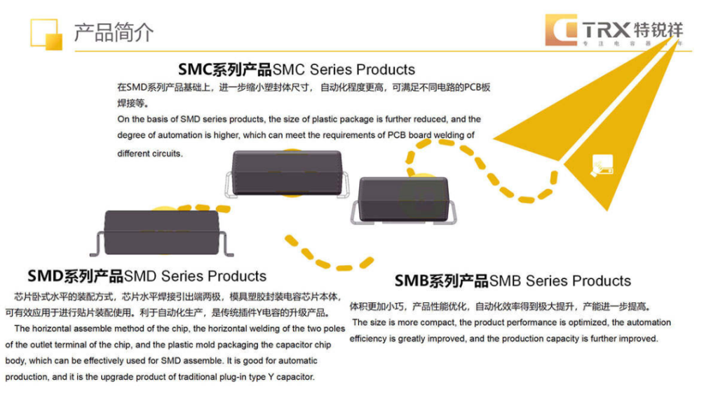
ChargerLAB has discovered that the TRX SMD-Y2 capacitors are utilized not only in dozens of fast-charging products from recognized brands like Belkin, Anker, QCY, Senicc, Mcdodo, OPPO, Lenovo, Nubia, Baseus, ARUN, and DIVI, but also in other products such as the Eaglerise 40W LED power supply, and the Changhong 42-inch smart TV 42P3F internal power supply. All of these products have received high praise for their outstanding performance.
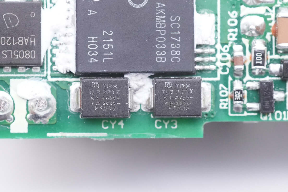
The other two SMD Y capacitors are also from TRX, but with a different model of TBY2221KB.
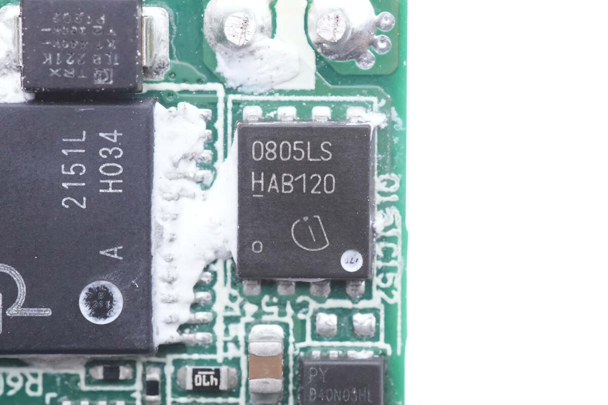
And the synchronous rectifier is from Infineon. 100V, 6mΩ for each. Model is BSC0805LS.
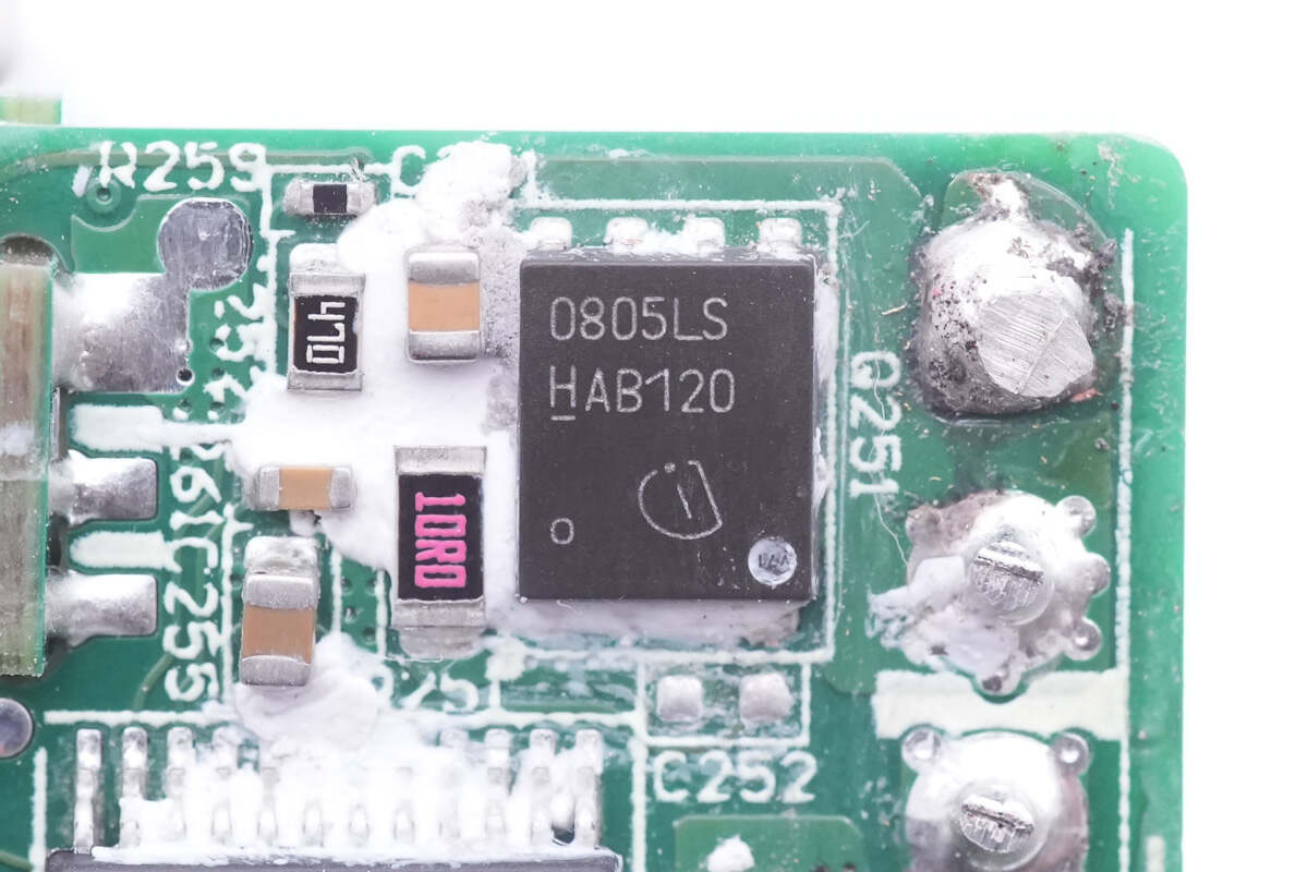
This synchronous rectifier is the same.
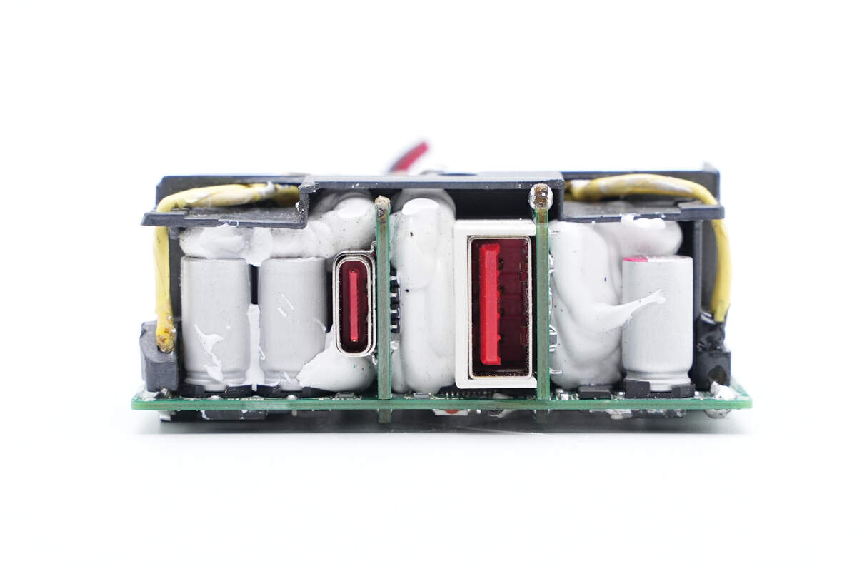
There're four solid capacitors and two USB ports on the output side.
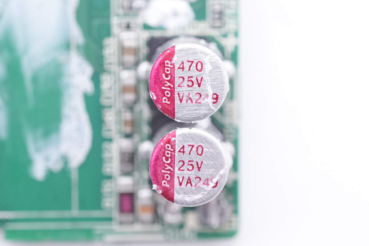
The solid capacitor for output filtering utilized in the charger is made by PolyCap, specifically their VA high-voltage SMD capacitor. Two capacitors are connected in parallel.
Further analysis has shown that PolyCaps' products are extensively applied in various areas such as chargers, car chargers, wireless chargers, power banks, and portable power stations. They are also frequently integrated into many products from well-known brands, including OPPO, vivo, Xiaomi, Honor, Samsung, Huawei, Lenovo, ZMI, Nubia, Bull, ANKER, and others. These products have been highly recognized within the market.
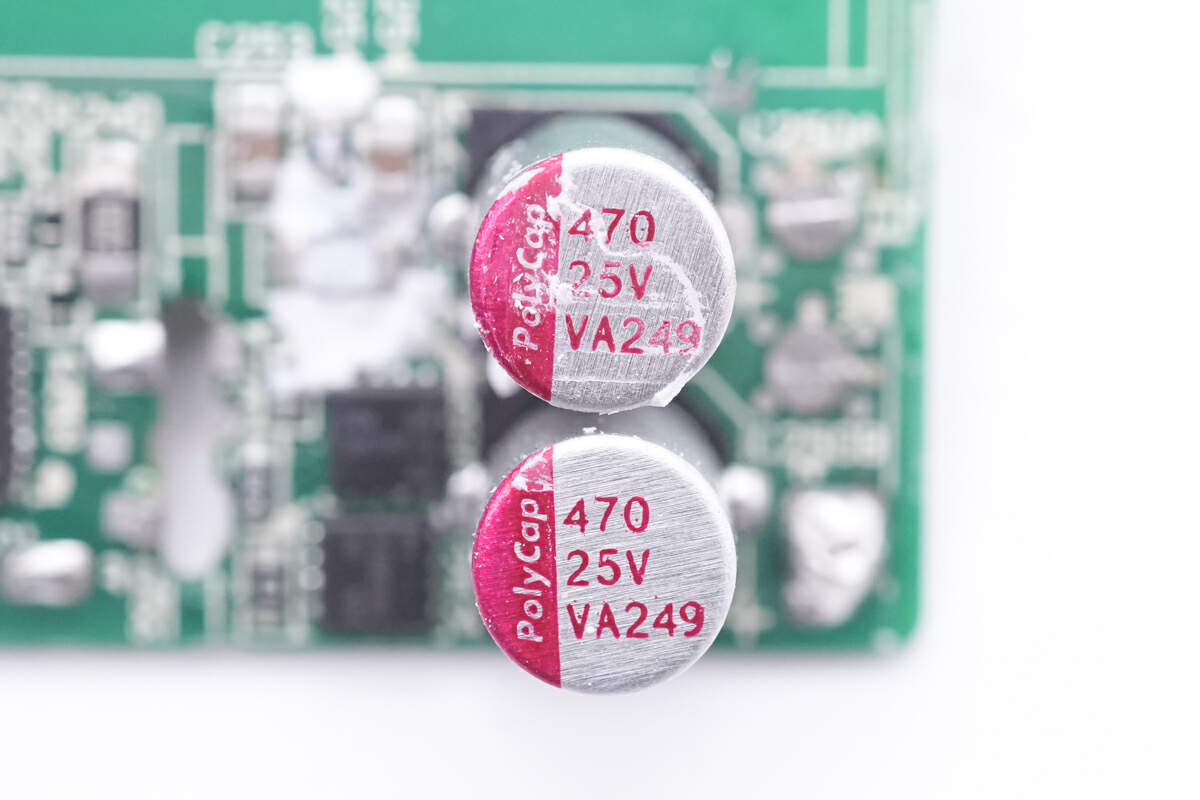
The other two solid capacitors are the same.
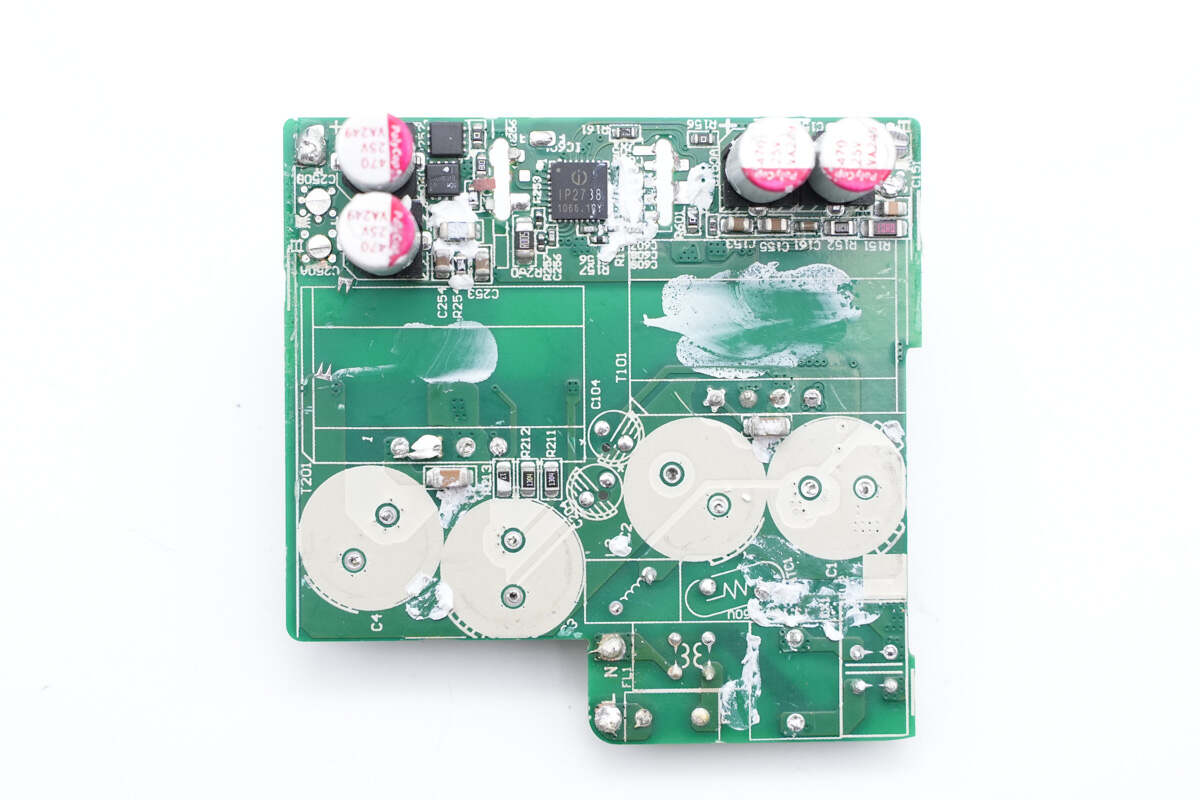
After removing all plug-in components, we can now see the protocol chip.
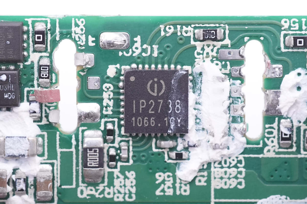
It employs the INJOINIC IP2738 as its protocol chip, which governs control of both output ports. The IP2738 is a dual-channel protocol chip intended for fast charging applications ranging from 18W to 140W. It boasts independent feedback control alongside independent USB PD control, just like integrating two IP2736 chips into one. Its fast-charging specifications are indistinguishable from those of the IP2736. Additionally, the chip supports USB PD3.1 28V EPR levels, as well as PD3.0/PPS and a broad range of other fast-charging protocols with excellent compatibility.
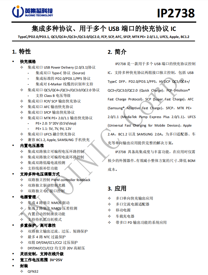
The INJOINIC IP2738 contains four independent NMOS drivers capable of controlling multiple ports. Its functionality includes switching multiple VBUS MOSFETs for output port switching, parallel control of two power supplies, and dual independent overcurrent, overvoltage, and short-circuit protections to ensure safe usage.
The INJOINIC IP2738 has previously been used in Mcdodo 40W dual USB-C GaN charger, L Lab 140W 2C1A GaN charger, Anker 65W 2C1A 2-in-1 GaN charger, and UGREEN 140W 2C1A GaN charger. Other fast-charging chips from INJOINIC have also been adopted by major brands including Xiaomi, Huawei, and Samsung, and have received high recognition from customers for their performance and quality.
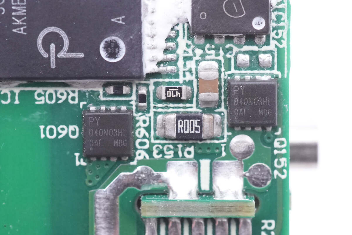
Two output VBUS MOSFETs marked with D40N03HL are from Pingwei, and the 5mΩ sampling resistor between them is used for output current detection.
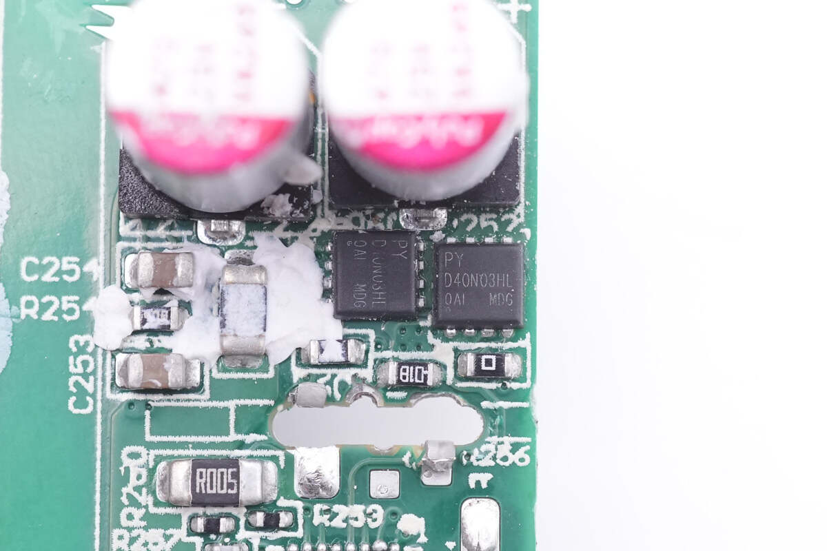
The other two output VBUS MOSFETs are the same, used to control the two independent output circuits.
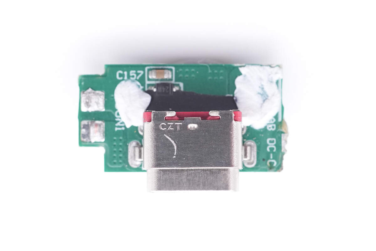
The USB-C connector is soldered on a separate small PCB and comes from CZT. The solder joints are sealed with adhesives to prevent any potential damage.
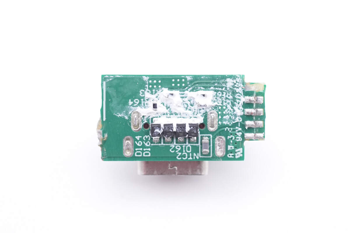
The TVS diode and thermistor are soldered on the back.
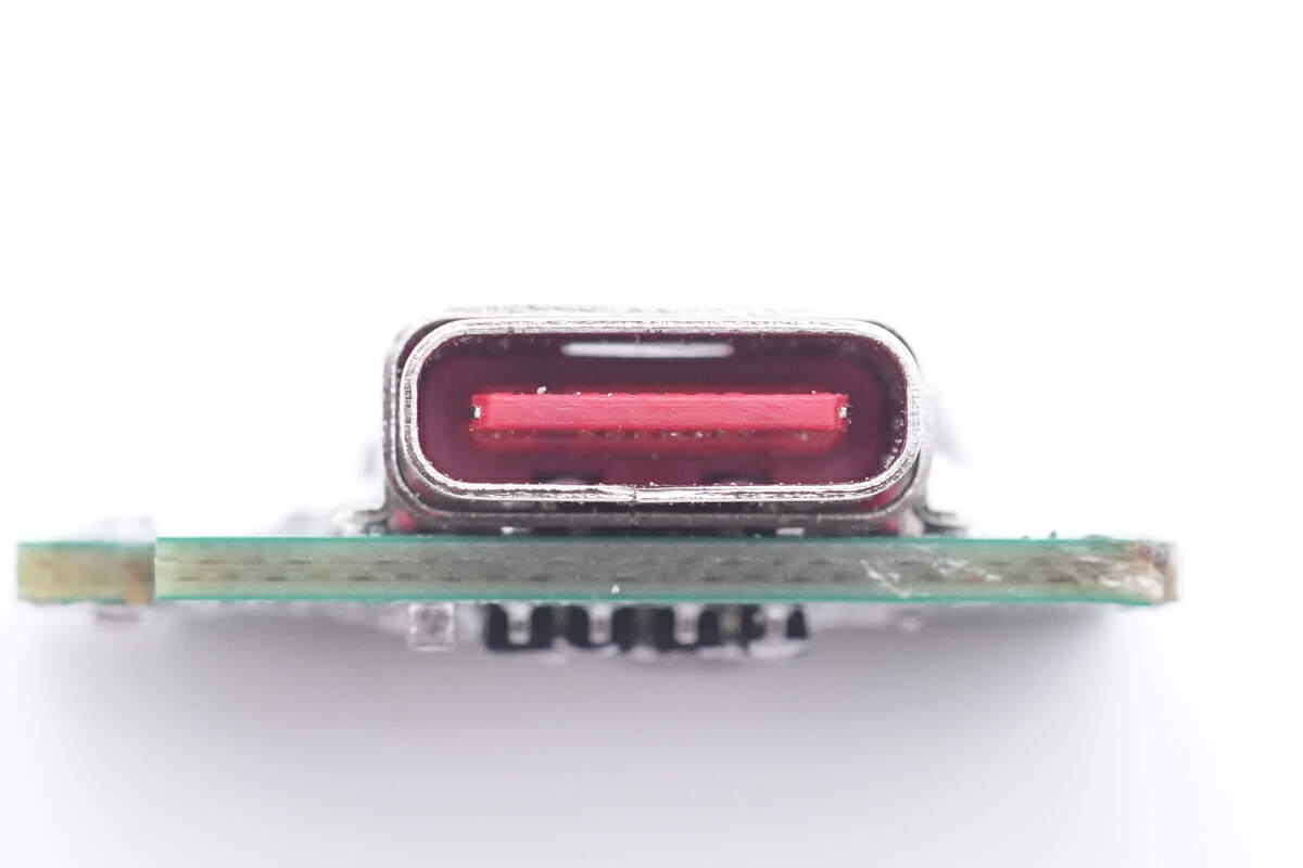
The plastic sheet inside the USB-C connector is red.
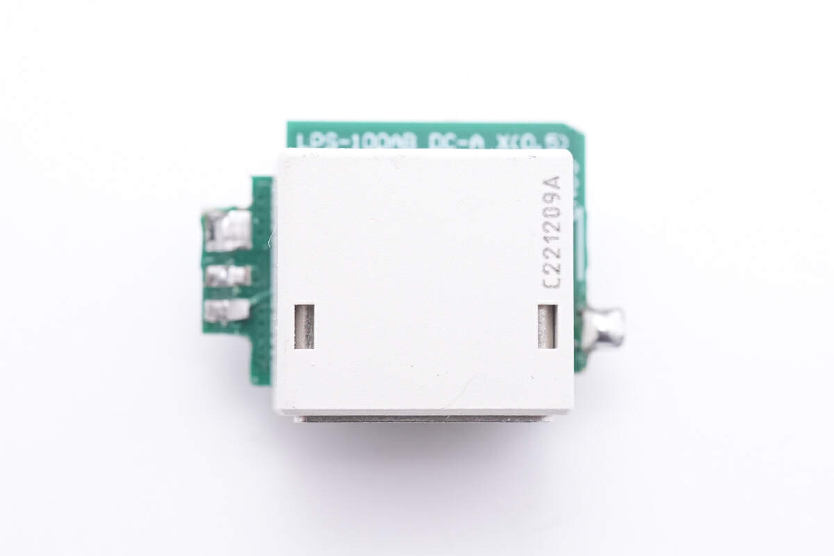
And the USB-A connector is insulated with white plastic shell.
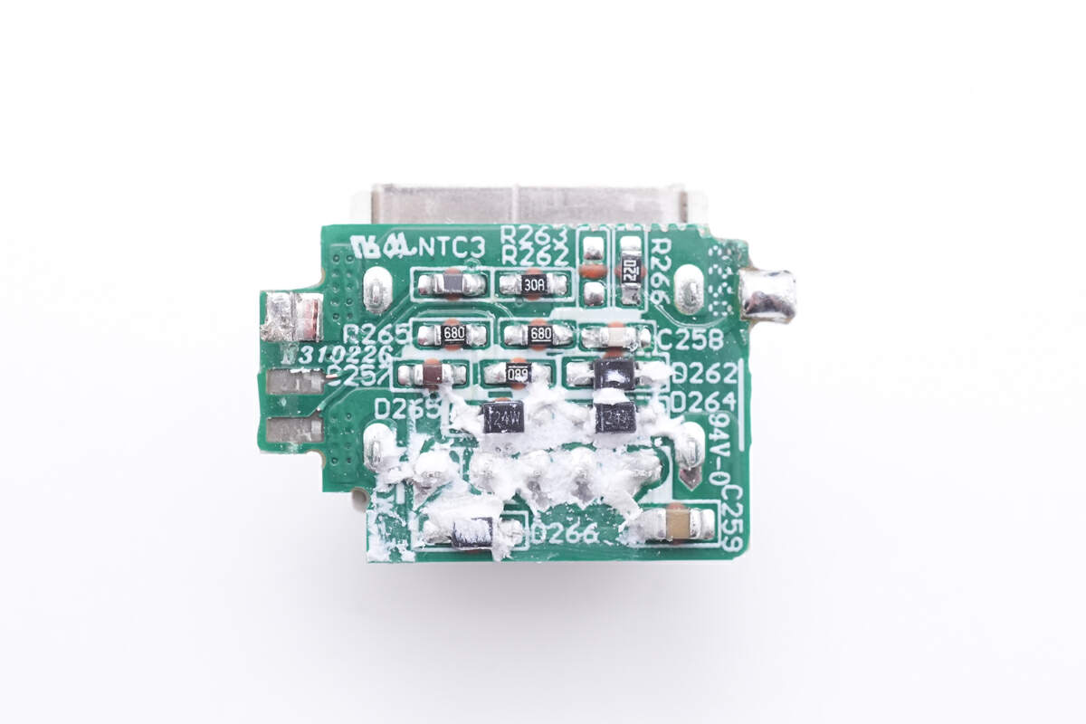
The TVS diode and thermistor are also soldered on the back of this PCB.
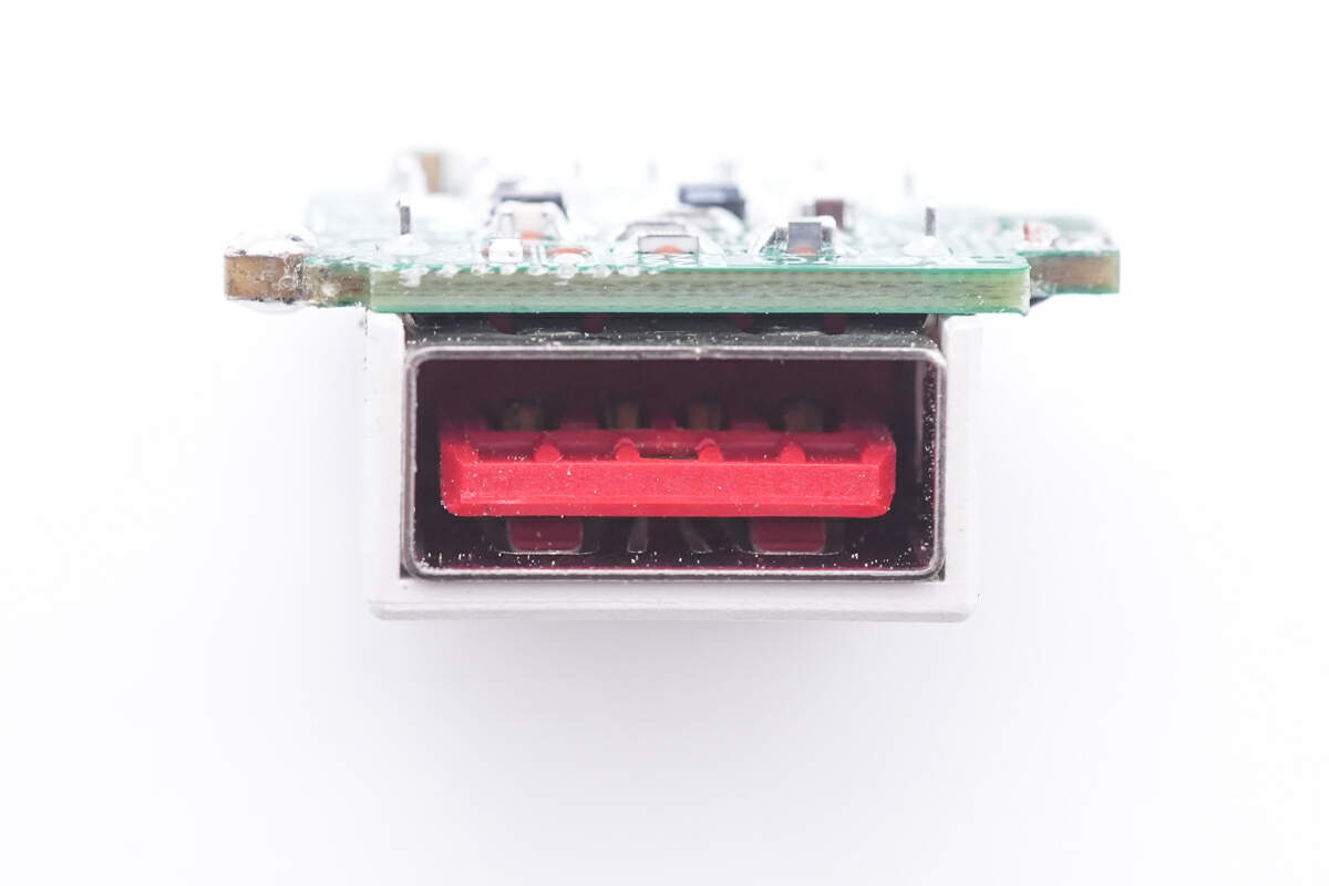
The USB-A connector is equipped with a red plastic sheet and its positive and negative poles are deliberately designed to be wider than traditional one. Additionally, it includes auxiliary contacts located at the front specifically for detecting original cables.
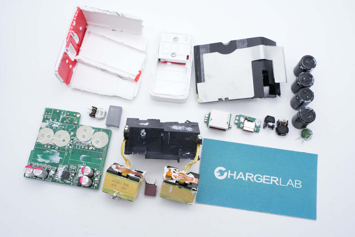
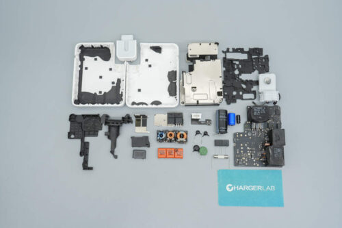
One last look at all the components of this OnePlus SUPERVOOC 100W Dual Ports Charger.
Summary of ChargerLAB
The OnePlus SUPERVOOC 100W Dual Ports Charger comes with both the USB-A and USB-C ports capable of supporting 100W Super Charge when used separately. It is easy to use with either a dual USB-C or normal cable for quick charging of your phone. In addition to the charger, a unique red cable is included, which can provide 100W fast charging for OnePlus phones and 65W power for the laptop, catering to the needs of users.
Upon disassembling the charger, a dual PI switch power chip set was uncovered along with an Ennochip IP2738 protocol chip. The SC1738C switch power chip can handle up to 50W output per unit, which reduces heating during power usage. The dual-switch power chips are controlled by the IP2738 protocol chip, providing independent output when used as a dual port with fast charging, and in parallel mode when used as a single port, providing higher power output.
Related Articles:
1. OnePlus Launched SUPERVOOC 100W Dual Ports Charger
2. Teardown of Oneplus Warp Charge 65W Power Adapter
3. Teardown of OnePlus SUPERVOOC 100W Dual Ports Charger (1A1C)

