Introduction
OnePlus has released an 80W GaN fast charger, called the OnePlus 80W SUPERVOOC USB-C Charger. This charger has a sleek white design with fixed prongs and supports both 5V2A and 11V6-7.3A output, as well as wide voltage input to meet the requirements of different countries. It features a single USB-C port that, when paired with a cable and phone that supports the SUPERVOOC protocol, can enable 80W SUPERVOOC charging. Next, ChargerLAB will provide a teardown of the OnePlus 80W GaN fast charger to reveal its internal components and build quality.
Product Appearance
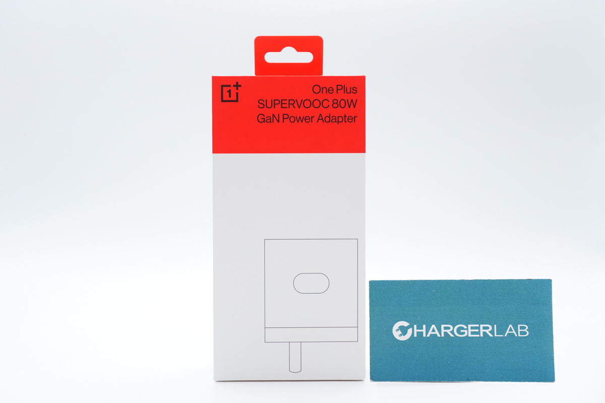
The packing design is almost identical to the OnePlus 100W dual port charger.
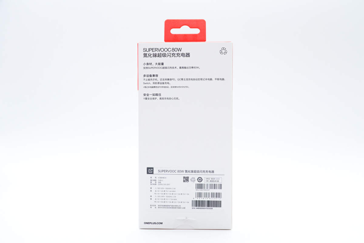
Some major selling points are on the back.
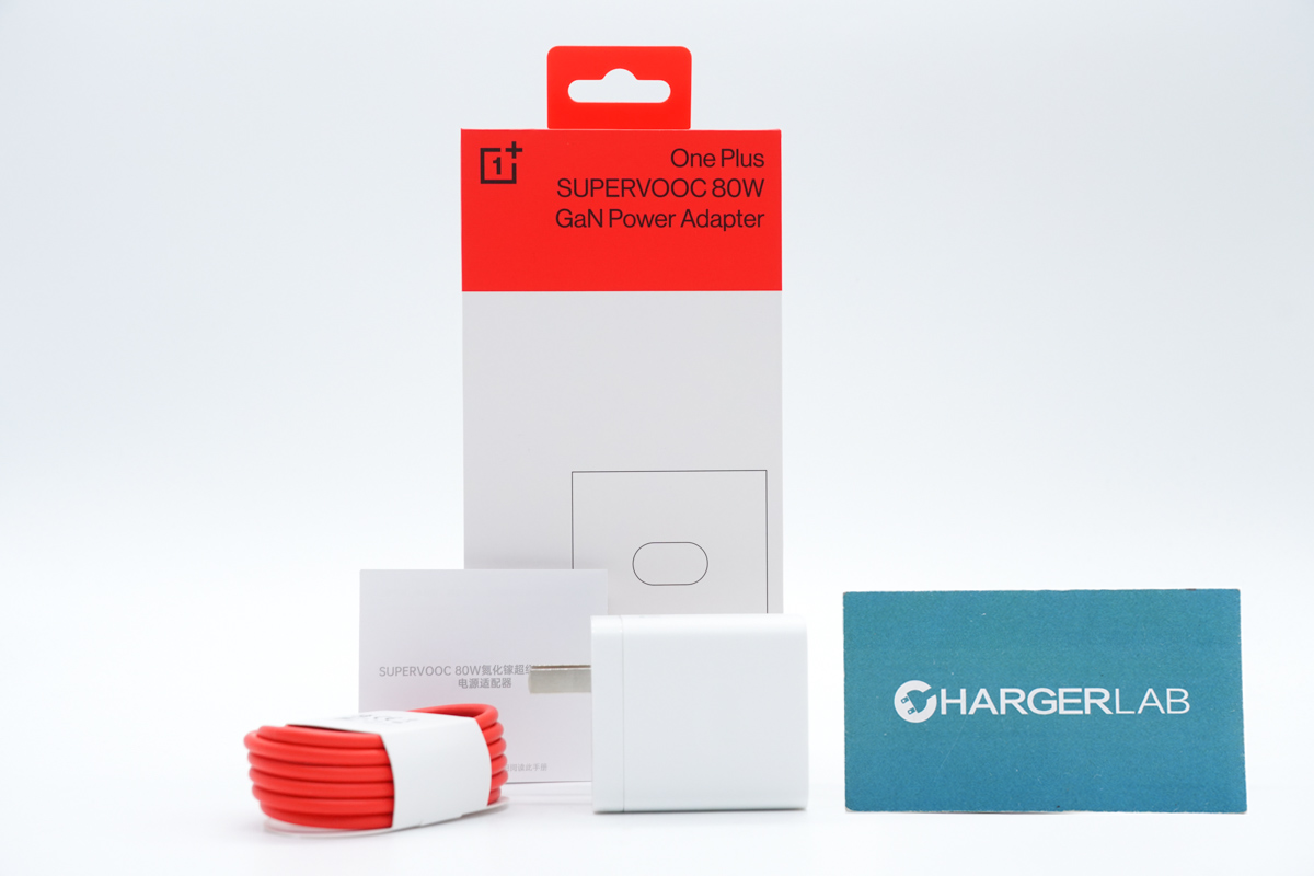
It contants an USB-C cable, some documents and the charger itself.
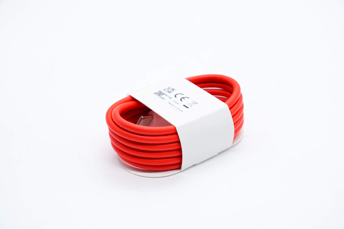
It's a classic OnePlus red cable.
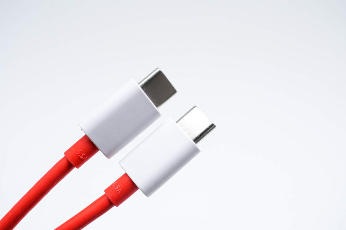
And it adopts dual USB-C port design.
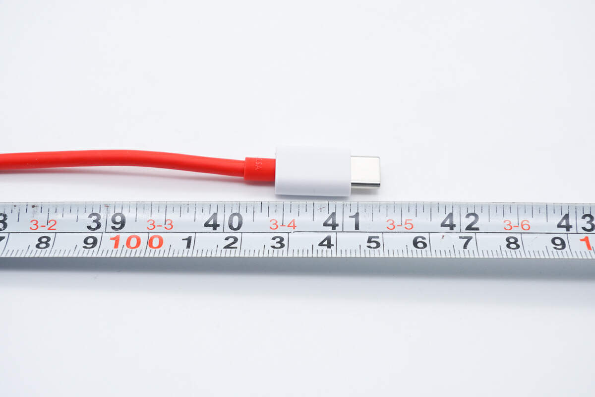
And the cable length is about 1m (3’ 3.37”).
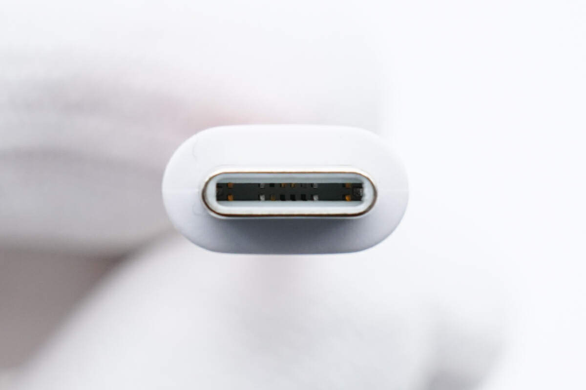
It doesn’t adopt a “full-pin” design.
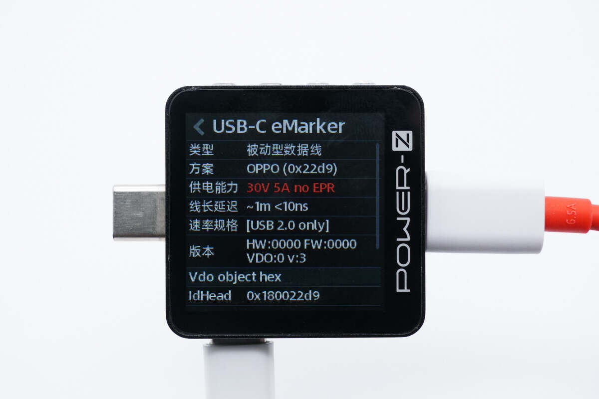
The ChargerLAB POWER-Z KM003C shows it integrates an E-Marker chip, but the data transmission speed is only USB 2.0.
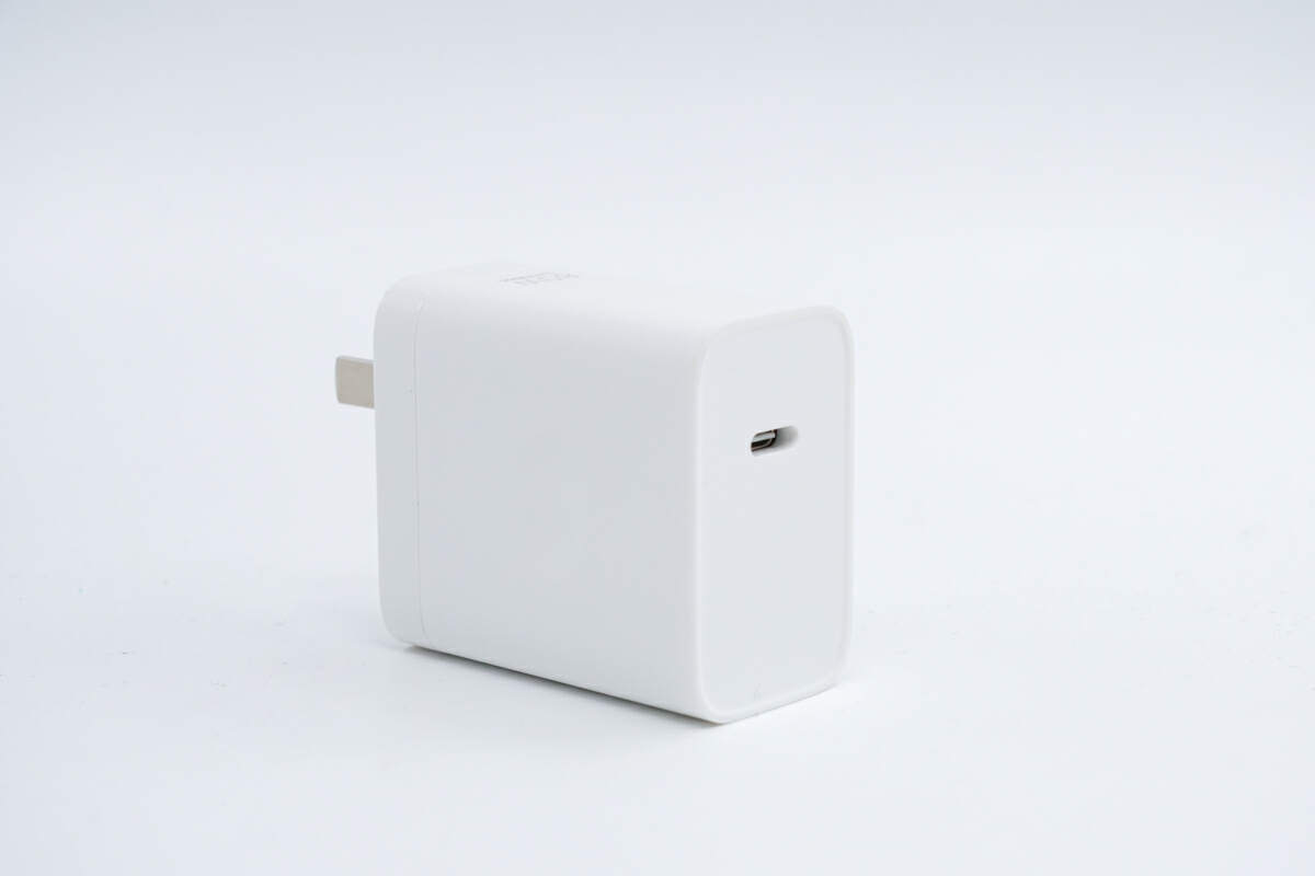
Unlike the traditional USB-A SUPERVOOC charger, it has a USB-C port.
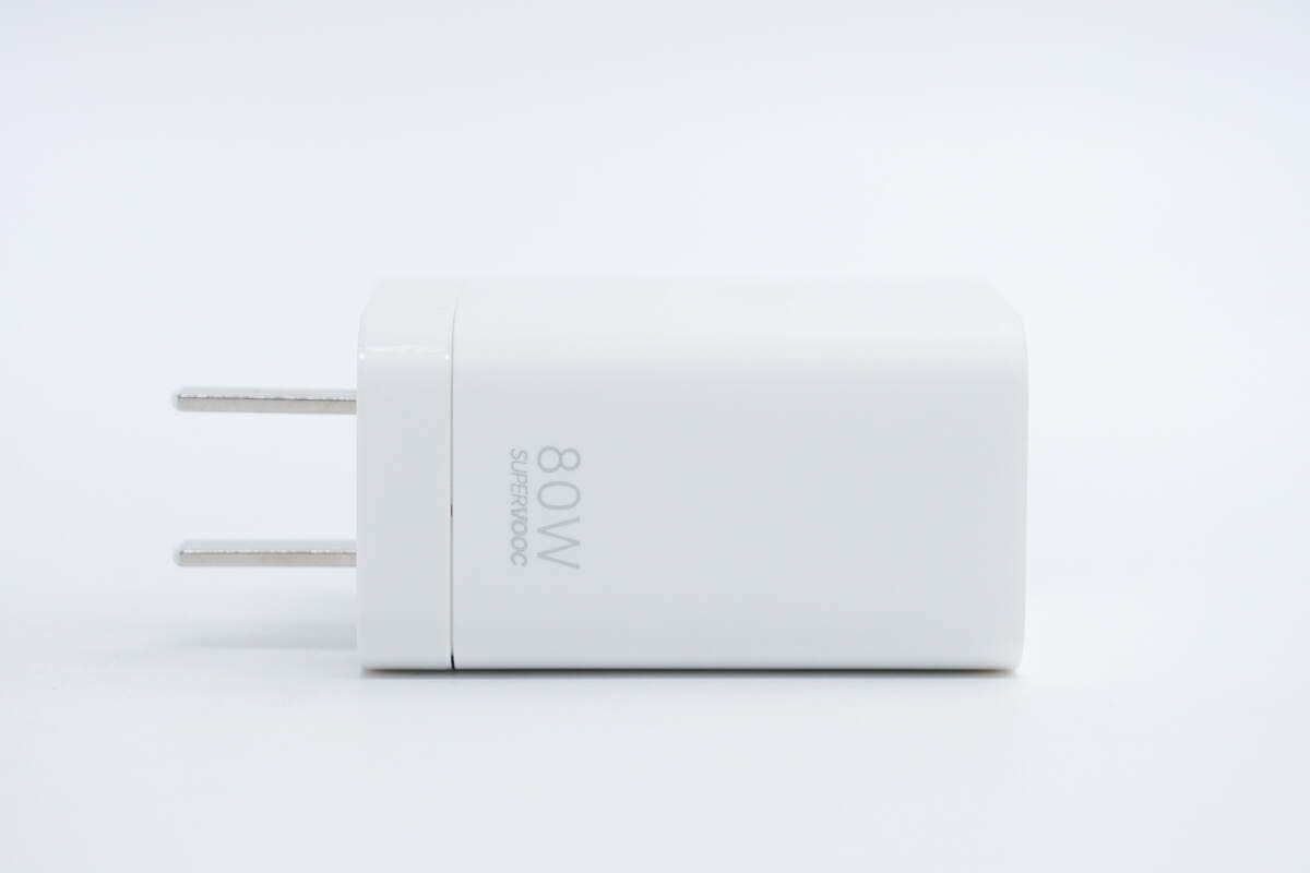
The 80W SUPERVOOC tells its maximum output power.

The slight hollows on two sides can facilitate the user to pull it out or plug it in.
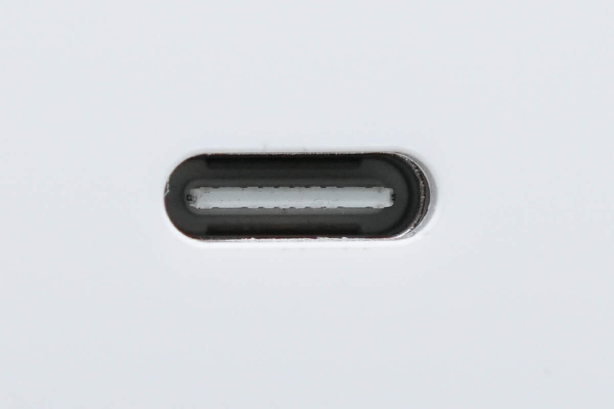
And the plastic sheet inside the USB-C port is white.
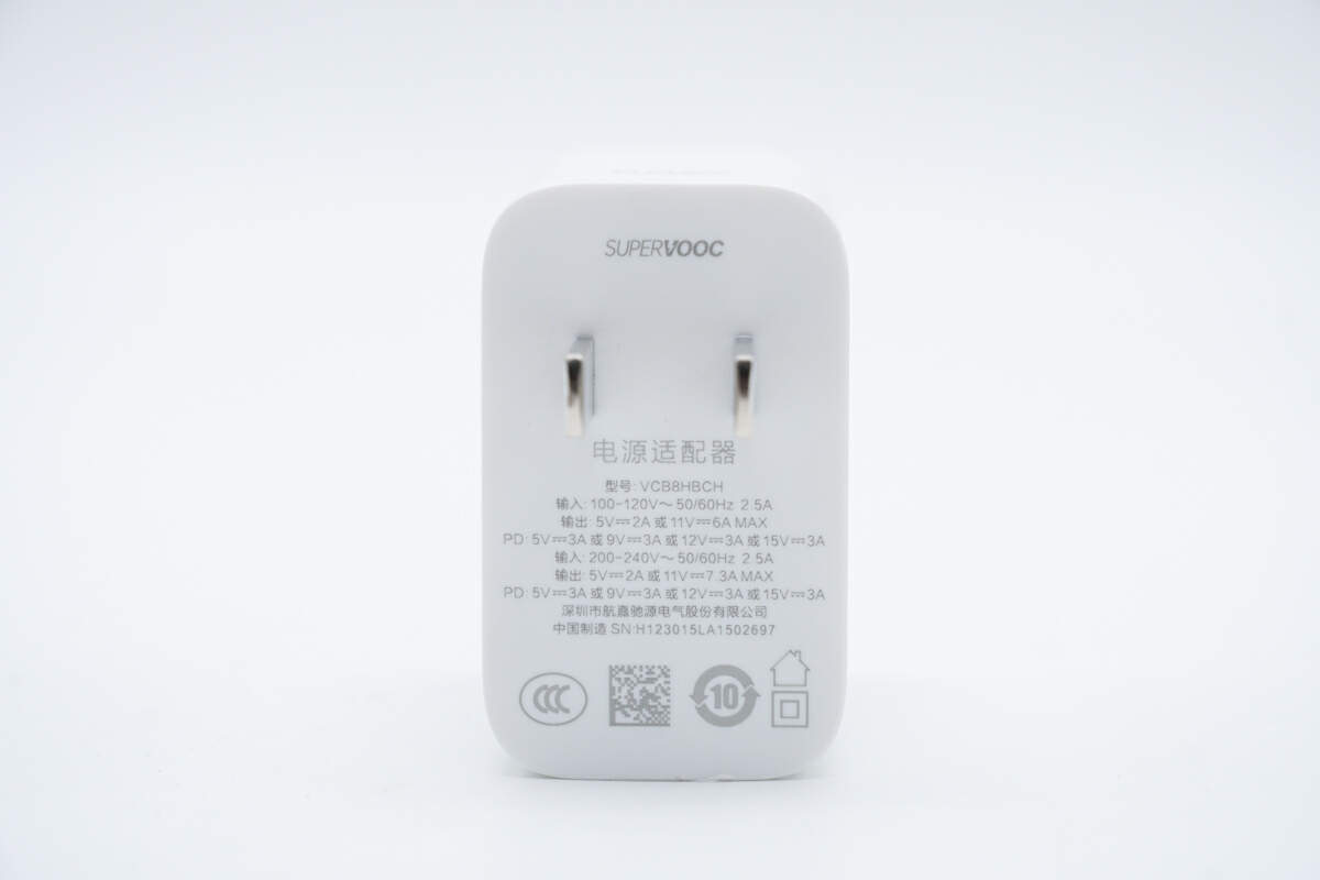
All spec info is printed under the fixed input prongs.
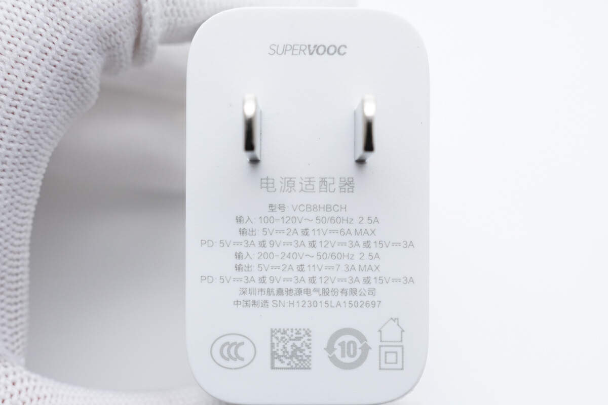
Model is VCB8HBCH. Like the 100W charger, it has different output power at different input voltages. It can reach 80W output at an input of 200-240V, and it only reaches 66W output at an input of 100-120V.
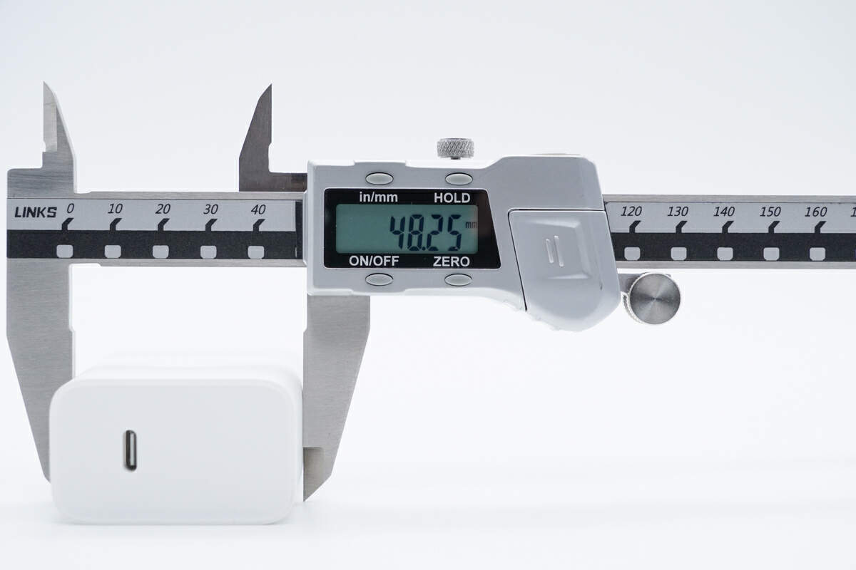
The length of the charger is about 48mm (1.89 inches).

The width is about 29mm (1.14 inches).
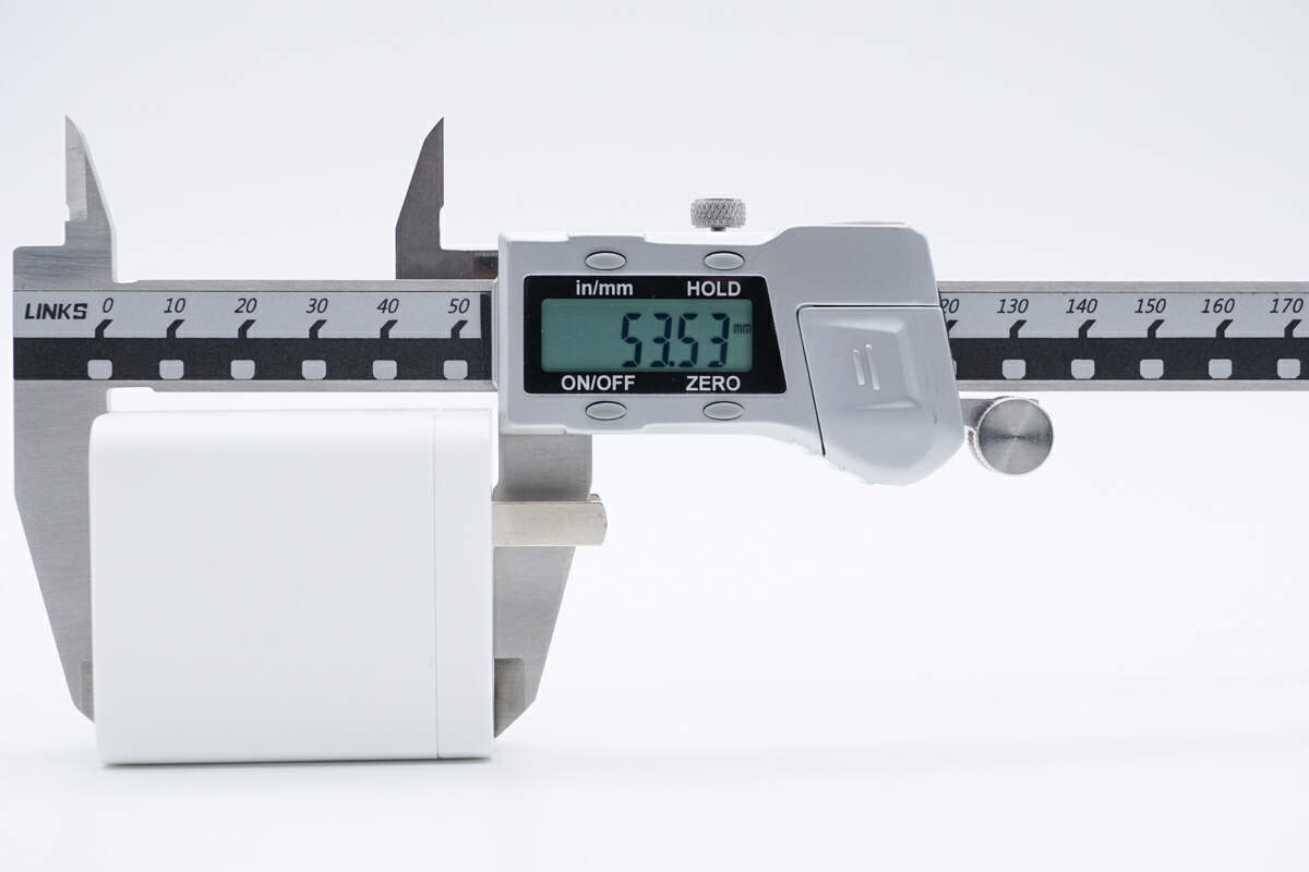
And the height is about 53.5mm (2.11 inches).
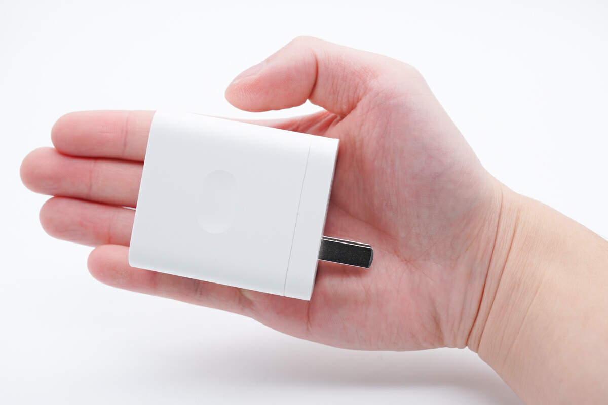
This is how it looks like on my hand.
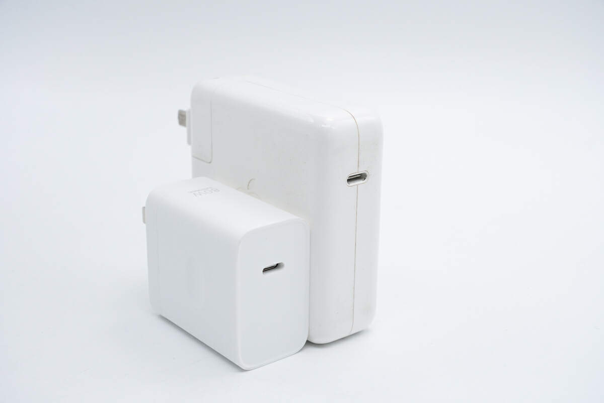
Compared with Apple 96W charger, it's much smaller.
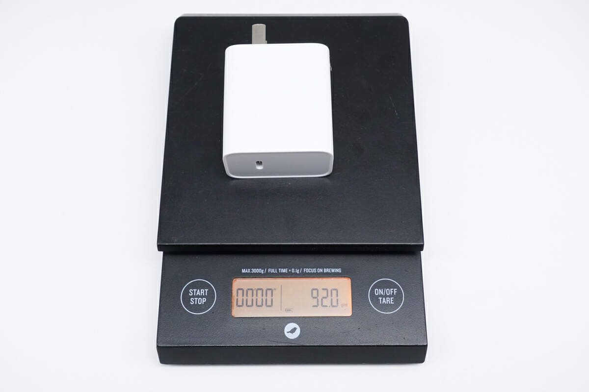
This charger is only 92g (3.25 oz).
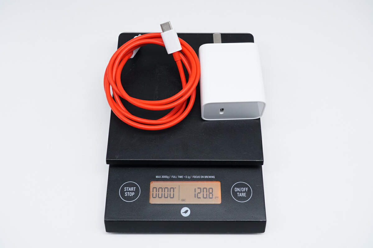
After adding the cable, the total weight is about 123g (4.34 oz).
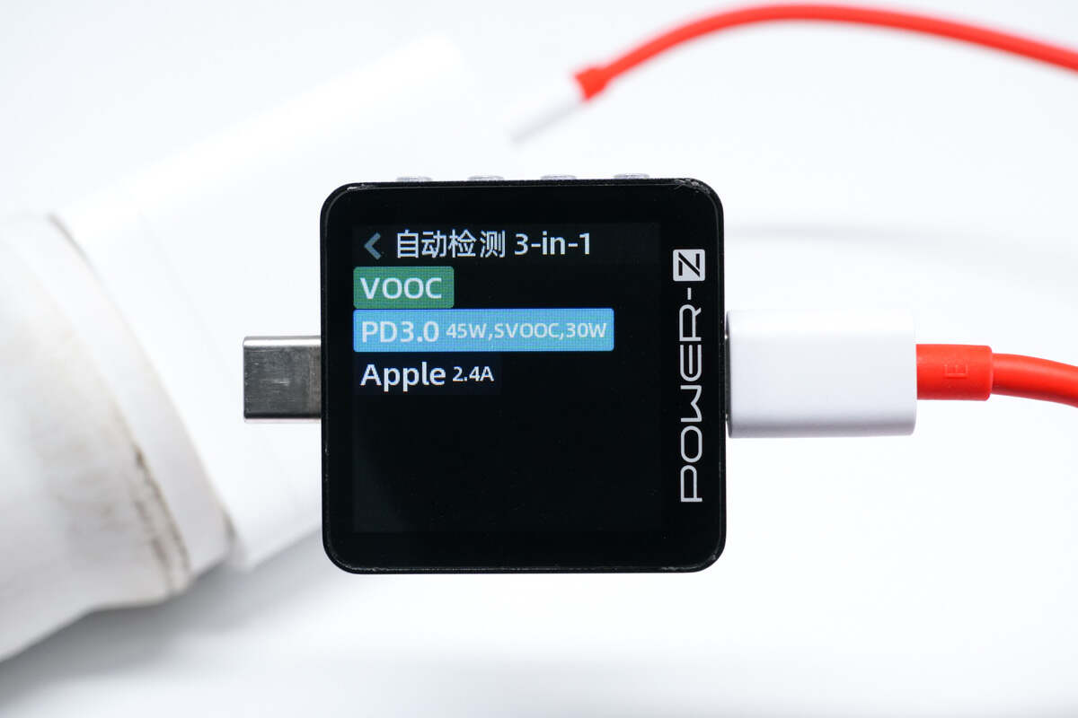
Our ChargerLAB POWER-Z KM003C shows it supports VOOC, SuperVOOC, and PD3.0 protocols.
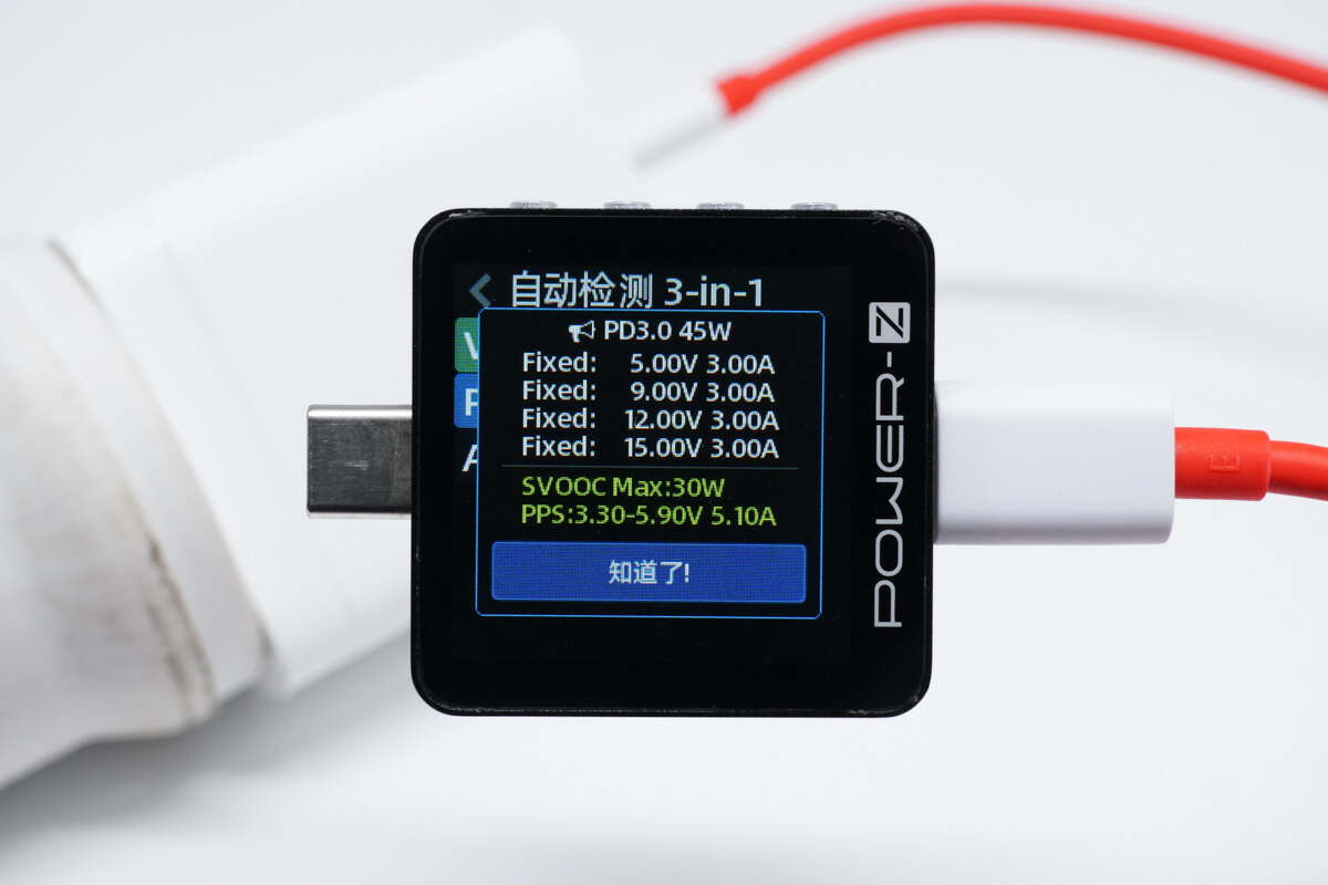
And it also has four fixed PDOs of 5V/9V/12V/15V 3A, and a set of PPS, so it can be compatible with 45W PD protocol.
Teardown
Now that we have completed our unboxing and testing of this OnePlus charger, it's time to take apart the device and examine its internal components and structure.
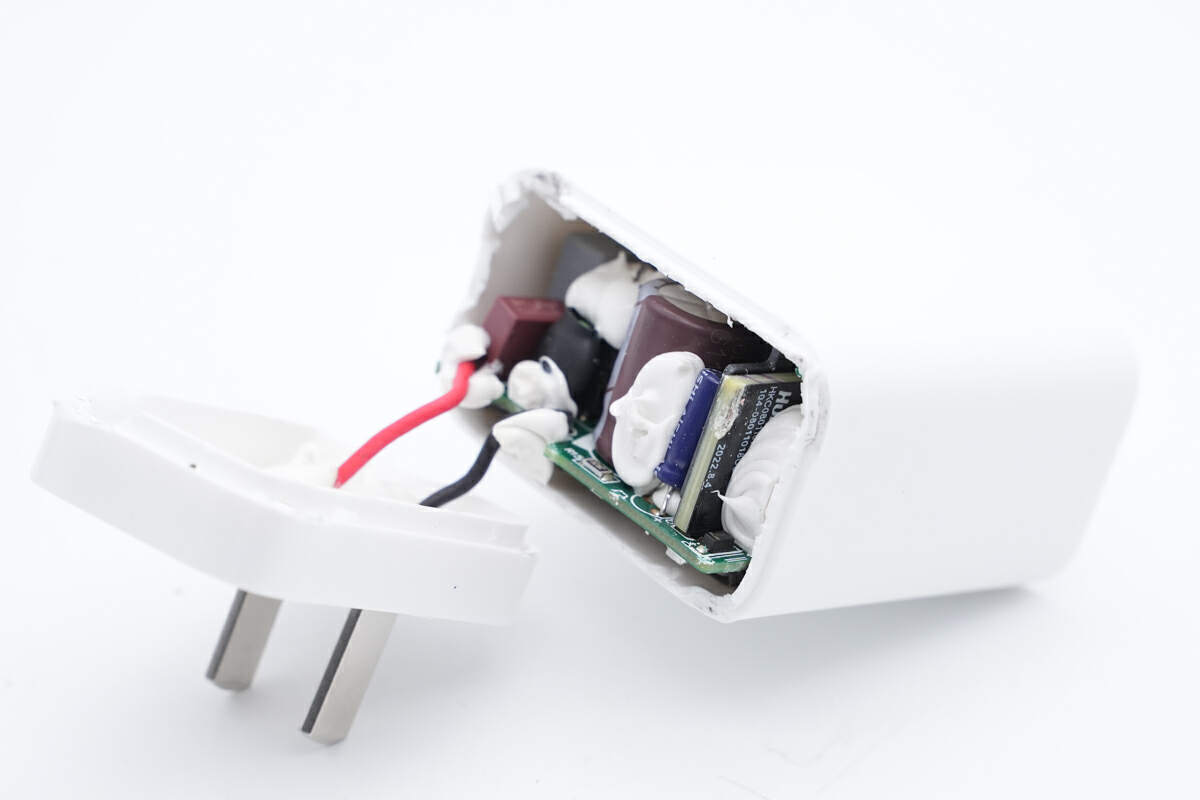
Use the spudger to pry along the gap, the black and red wires are connected to the input prongs.
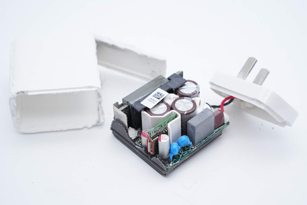
Continue to cut off the plastic case.
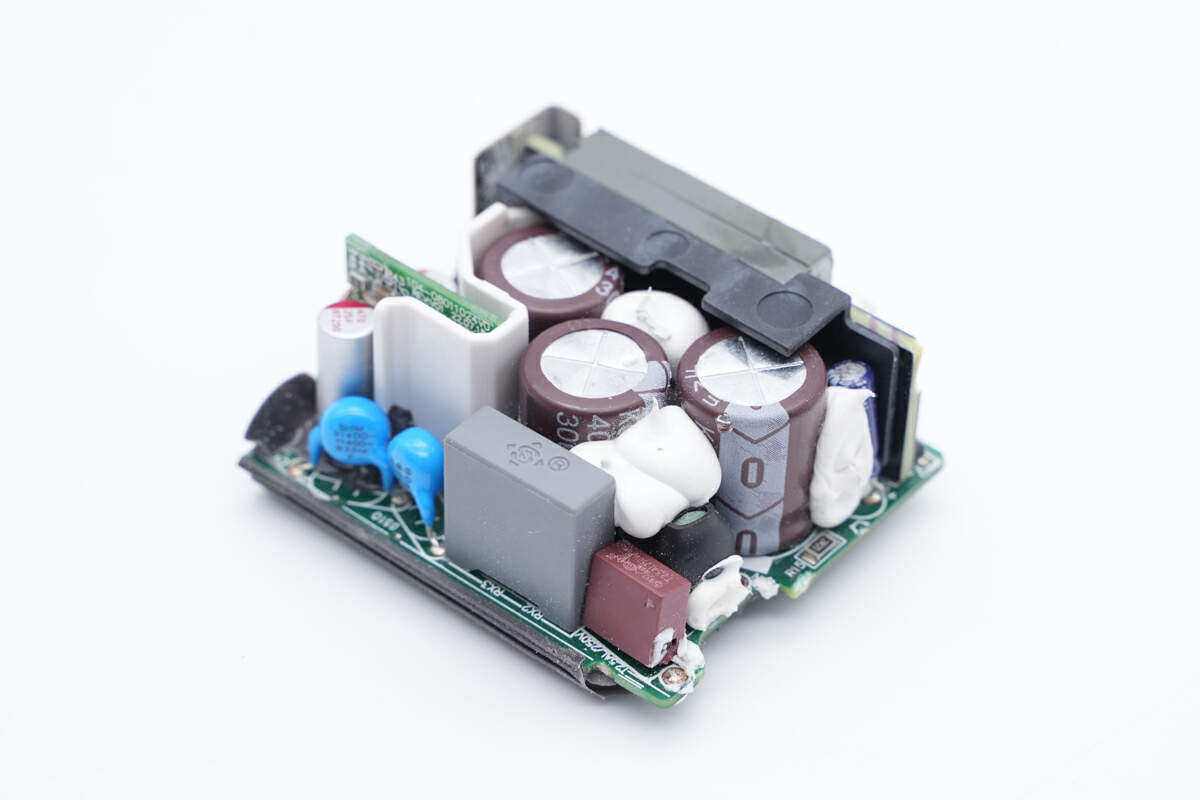
All plug-in components are on the front.
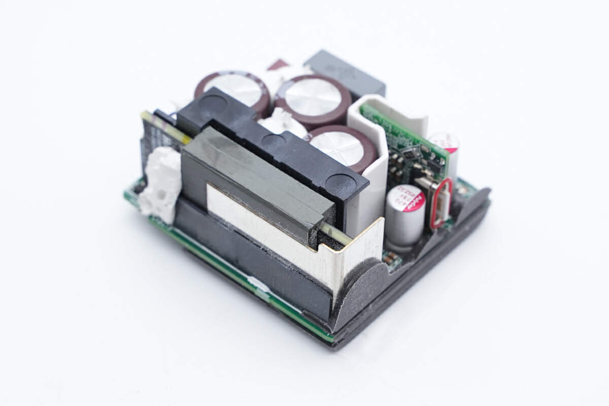
The planar transformer is on the side.
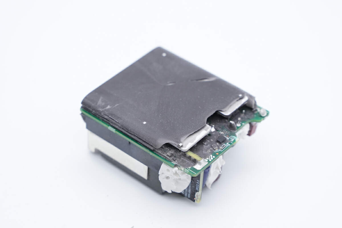
Here is the potting compound, which can improve the heat dissipation performance.
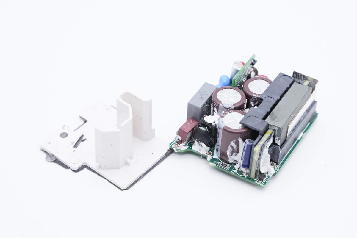
And the output PCB of the USB-C port is insulated by this white plastic plate.
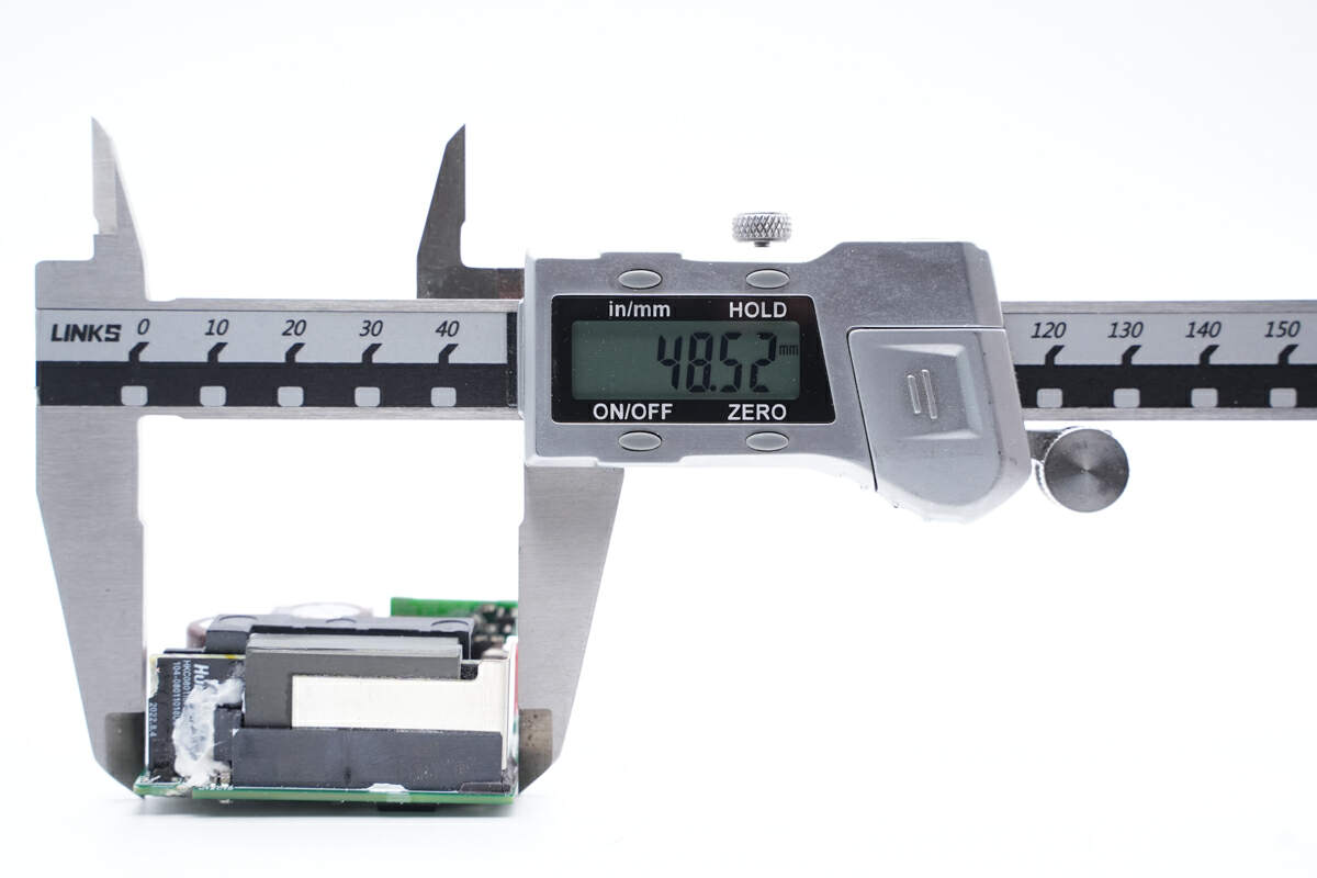
The length of the PCBA is about 48.5mm (1.91 inches).
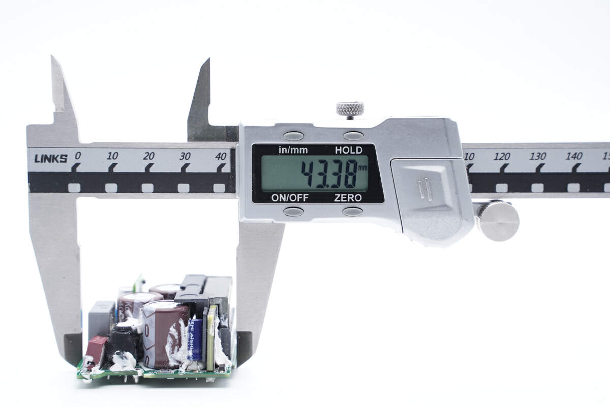
The width is about 43.4mm (1.71 inches).
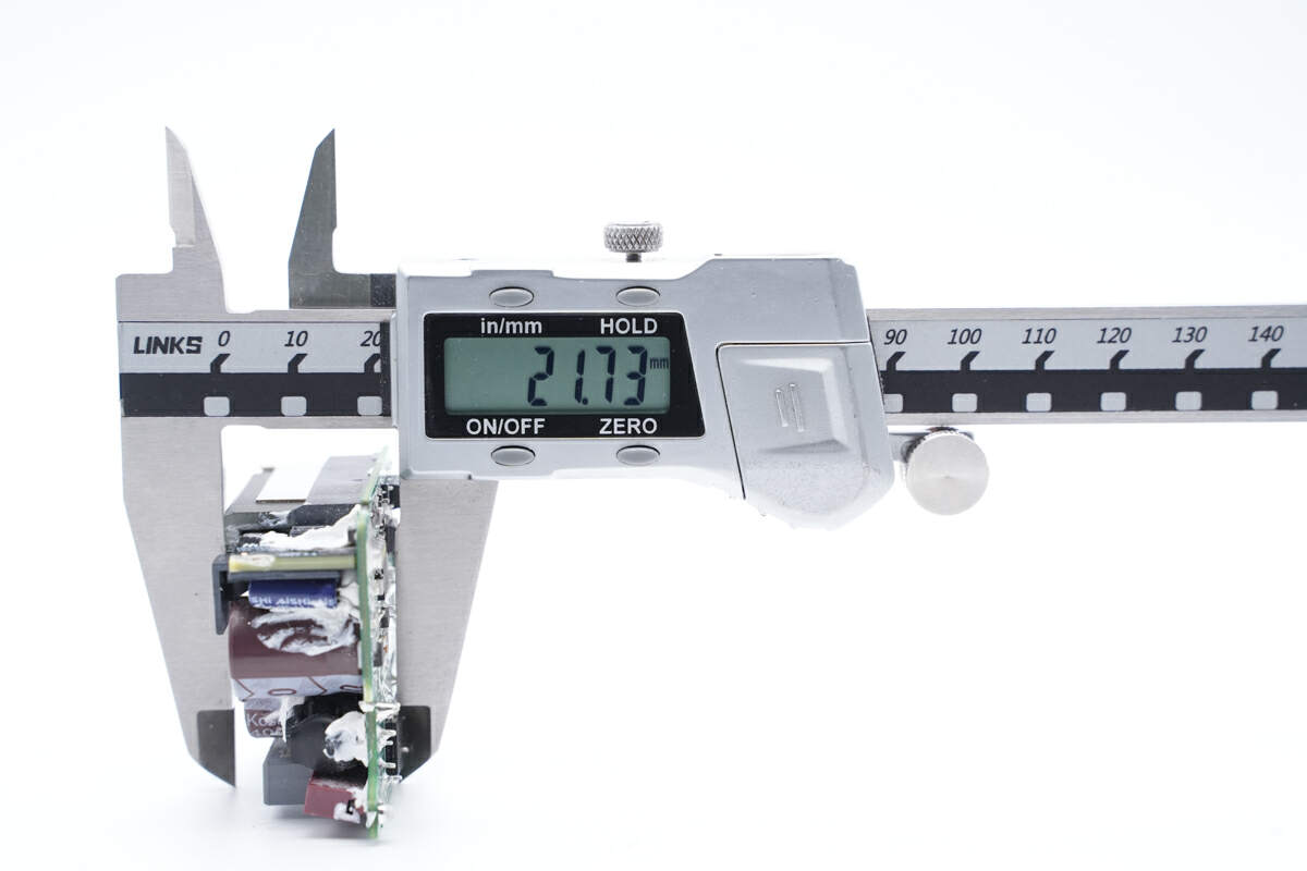
And the height is about 21.7mm (0.85 inches).
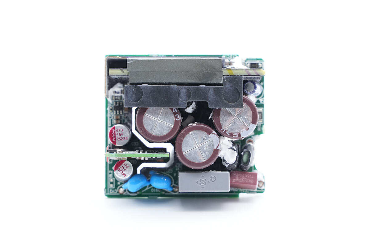
The fuse, NTC thermistor, common mode choke, safety X2 capacitor, planar transformer, and blue Y capacitor are on the front of the PCBA module.
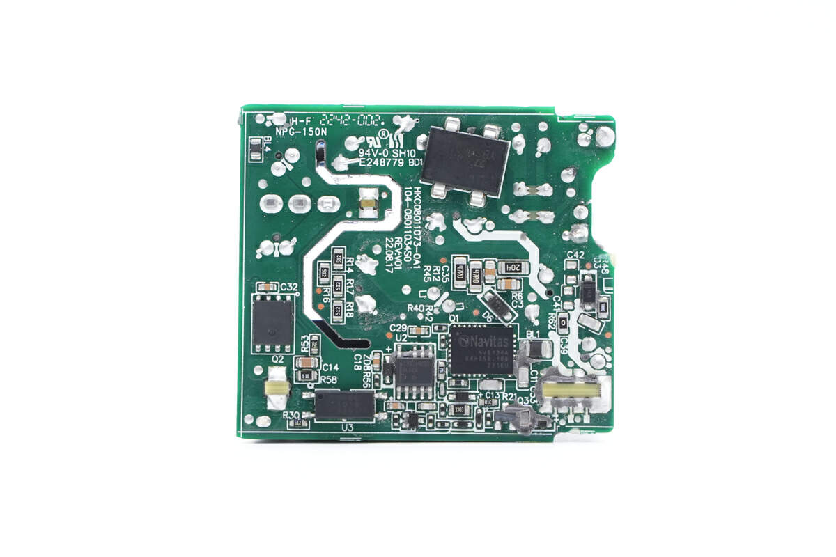
And the bridge rectifier, master control chip, GaN power chip, feedback optocoupler and synchronous rectifier are on the back.
ChargerLAB found it adopts QR flyback topology, and it does not have a PFC circuit. The current will be filtered by synchronous rectification circuit for output, and the output voltage is controlled by the protocol chip.
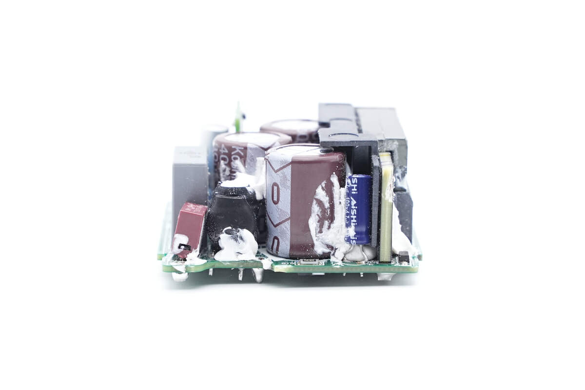
Next, let’s introduce every single component.
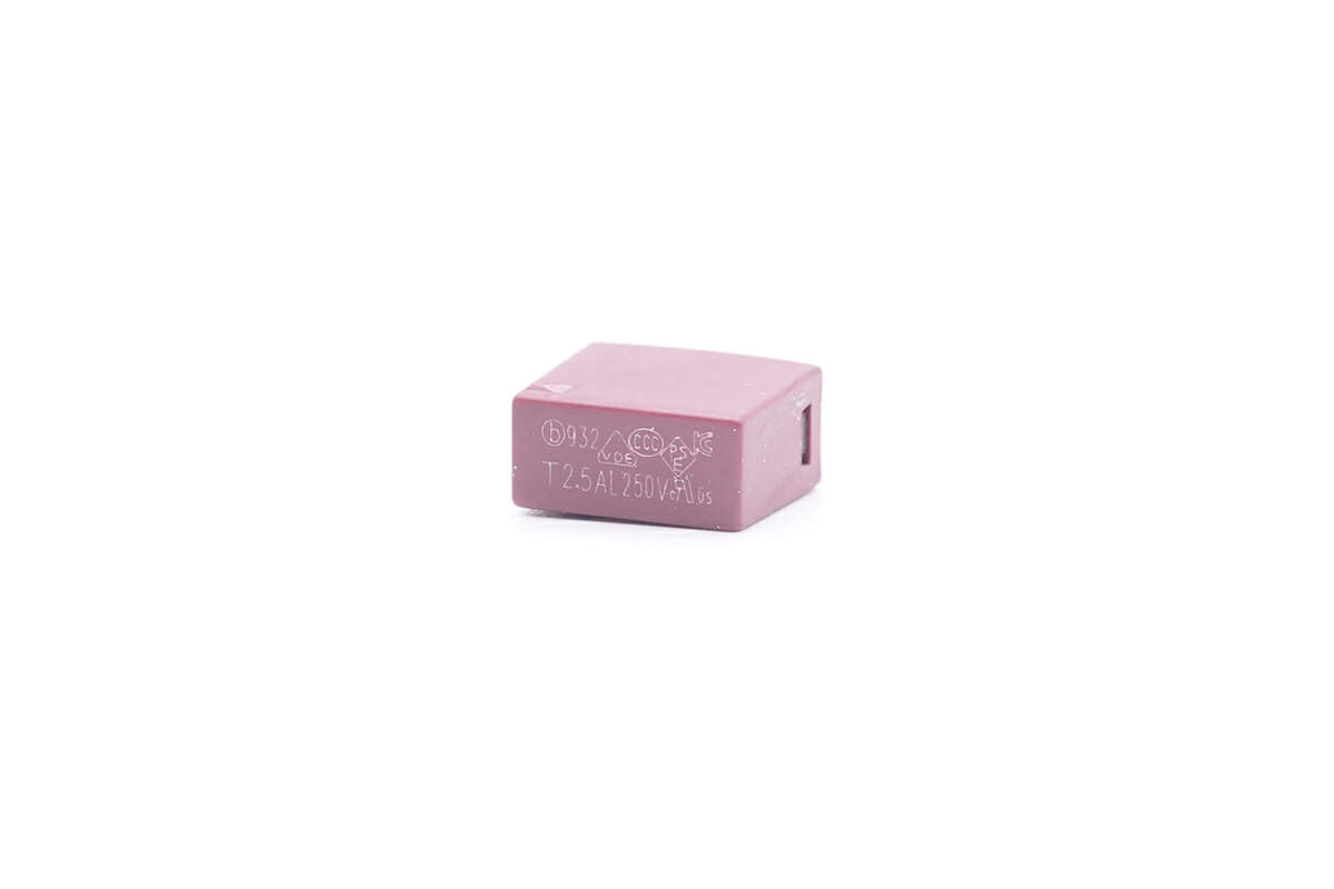
The input time-delay fuse is from Better Electronics. 2.5A 250V.
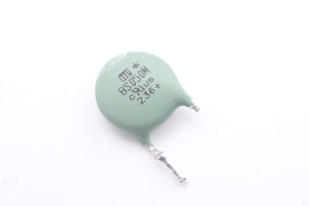
The NTC thermistor is from JOYIN, model 8S050M, which is used to suppress the inrush current when plugged in.
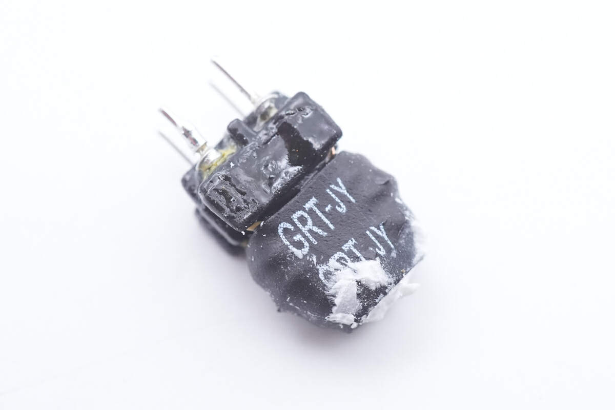
The common mode choke is insulated with heat-shrinkable tubing.
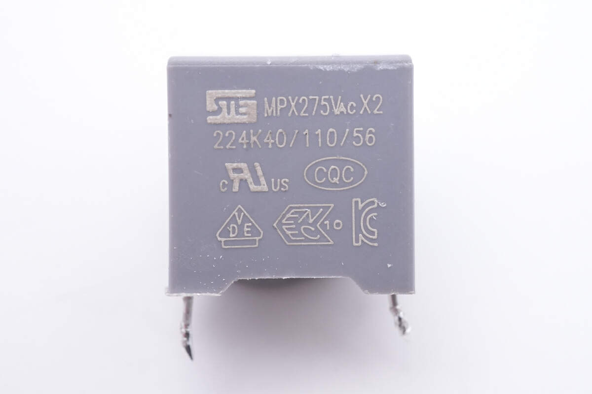
The safety X2 capacitor is from STE. 0.22μF.
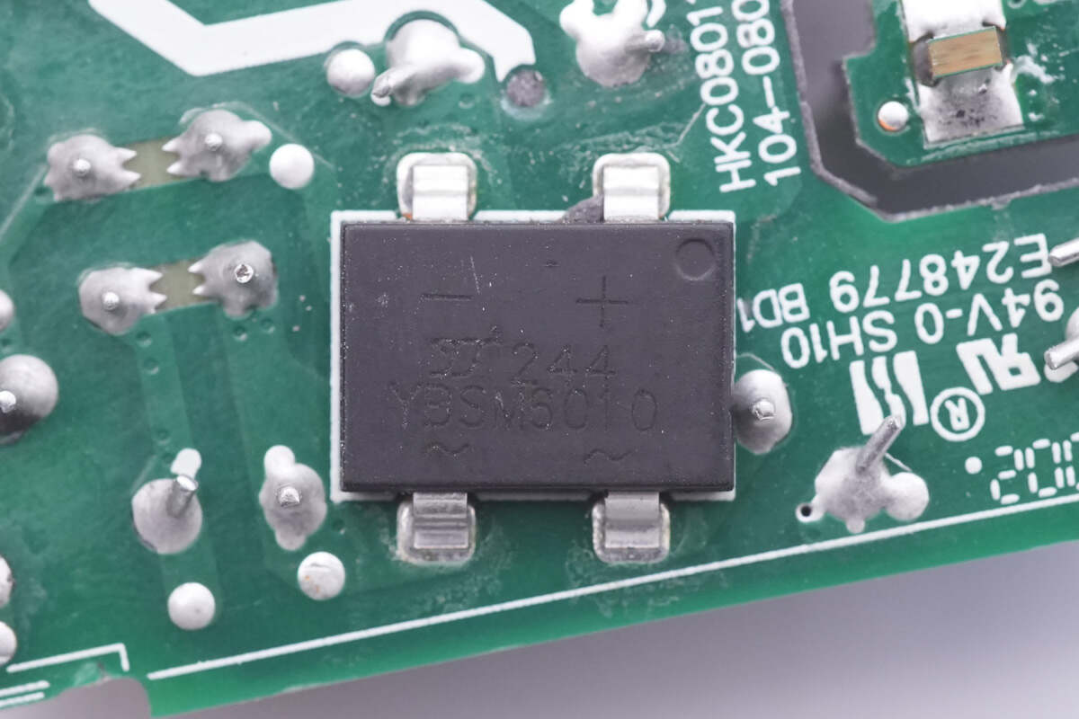
This bridge rectifier is from Yangjie. Model is YBSM6010. 6A 1000V.
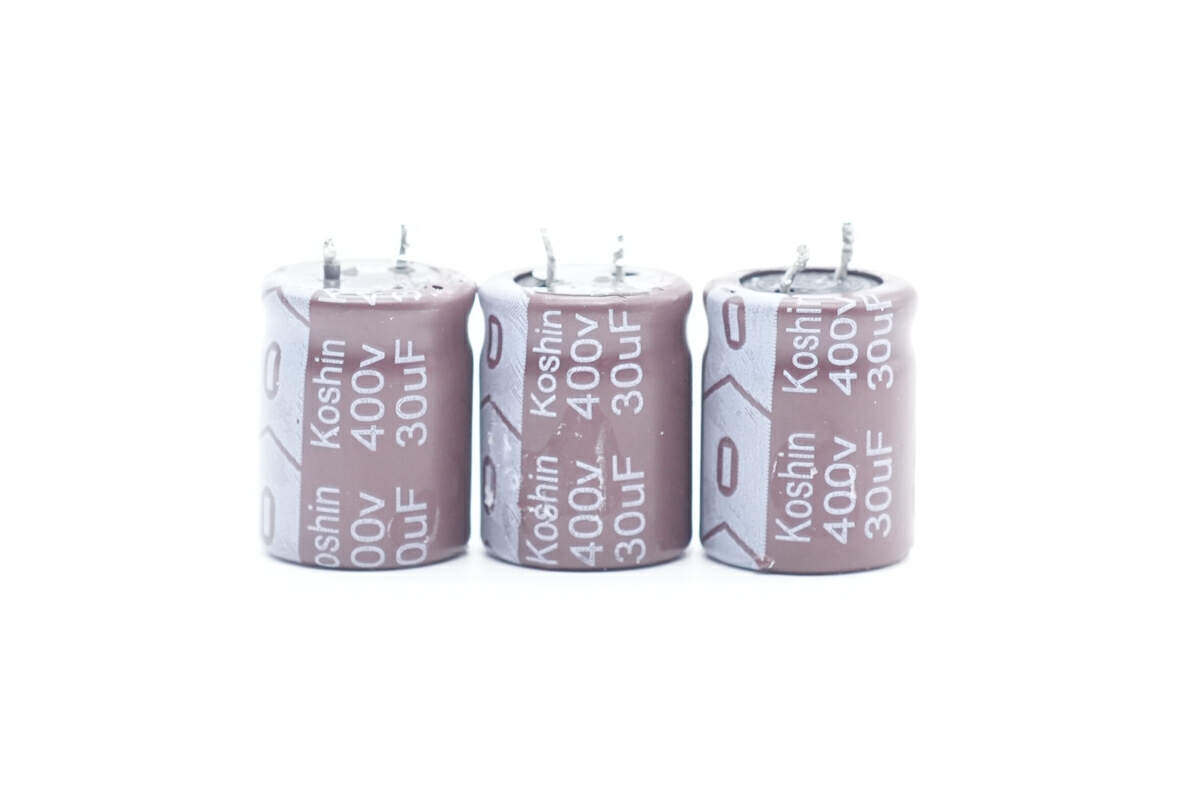
Those three electrolytic capacitors for input filtering are from Koshin, 400V 33μF for each, 99μF in total.
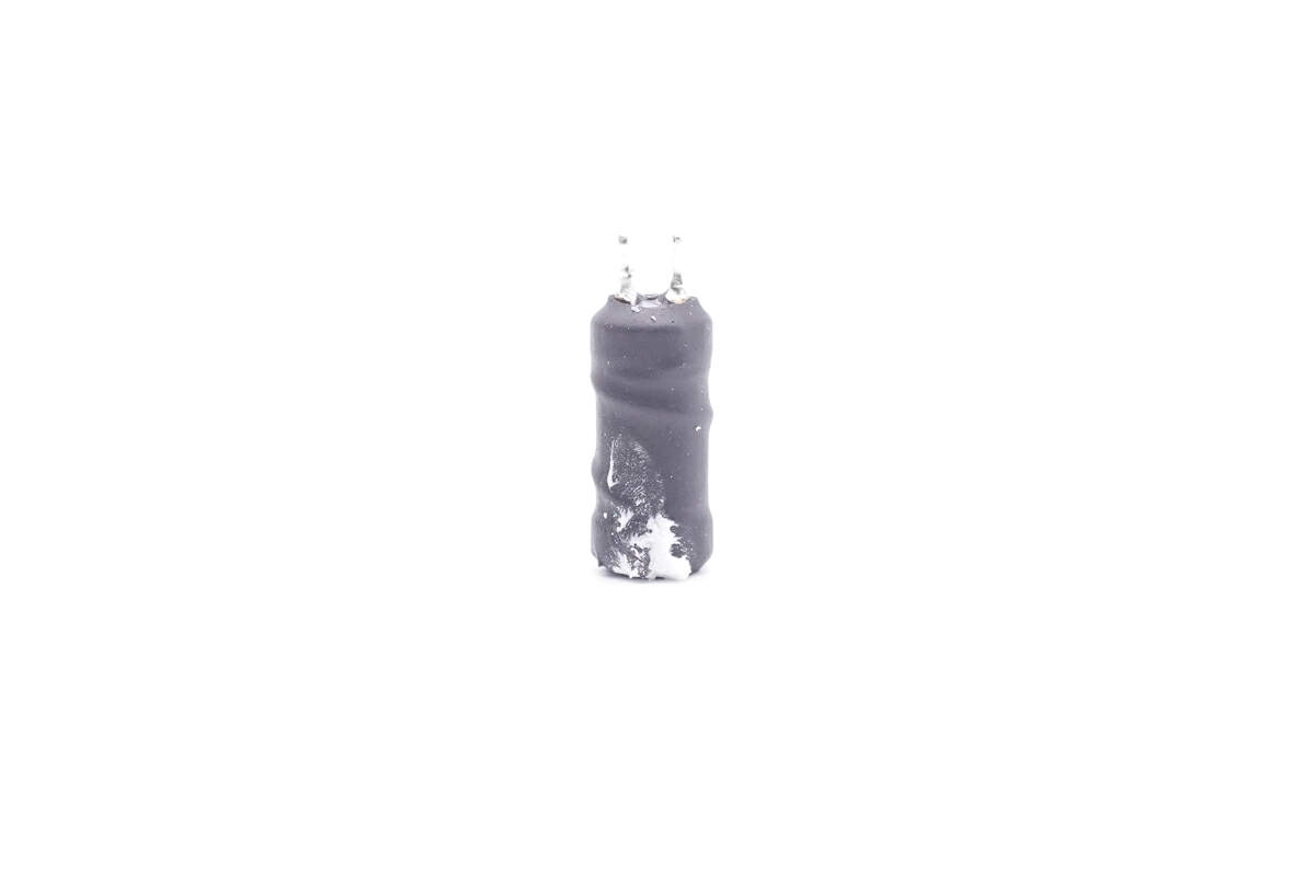
The differential mode choke adopts an I-shaped magnetic core.
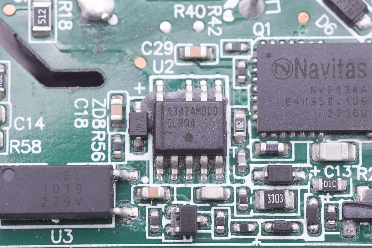
The master control chip is from ON Semiconductor, model NCP1342, which is a high-frequency QR flyback controller. It integrates active X2 capacitor discharge and supports wide range Vcc power supply.
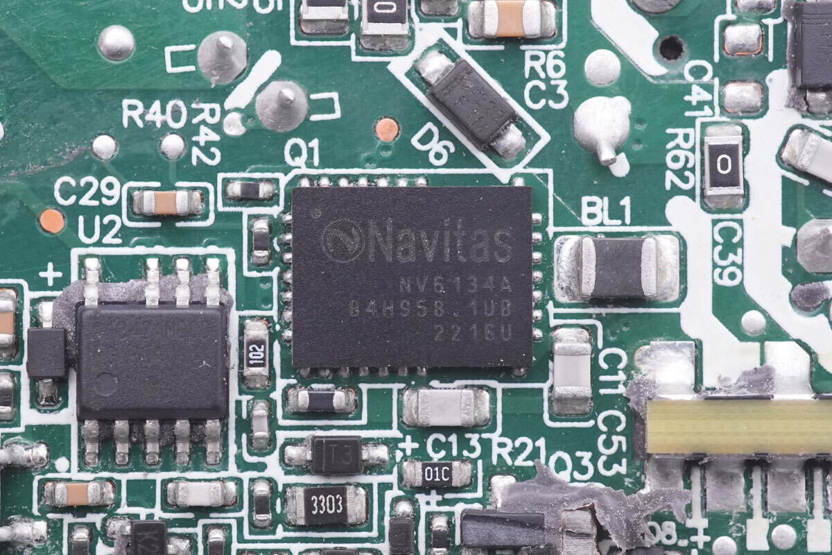
The GaN IC for QR topology is from Navitas, model NV6134A, and adopts QFN6 x 8 package. It integrates GaN FET, driver, and GaNSense lossless current sampling circuit.
Without an external sampling resistor, it can reduce cost and improve efficiency.
It's also the latest GaN power IC of the GaNFast series. It can improve charger efficiency, reduces heat, and can save more space. It also has over-temperature, over-current, and other protections, ensuring the charger's reliability.
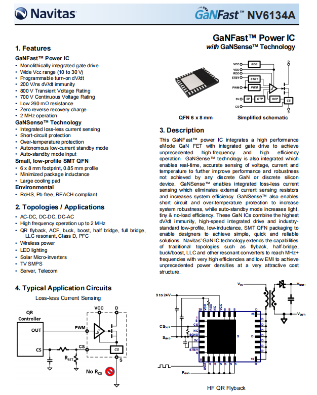
Here is all the information about Navitas NV6134A.

This tiny capacitor is from AiShi, which powers the master control chip. 100V 4.7μF.
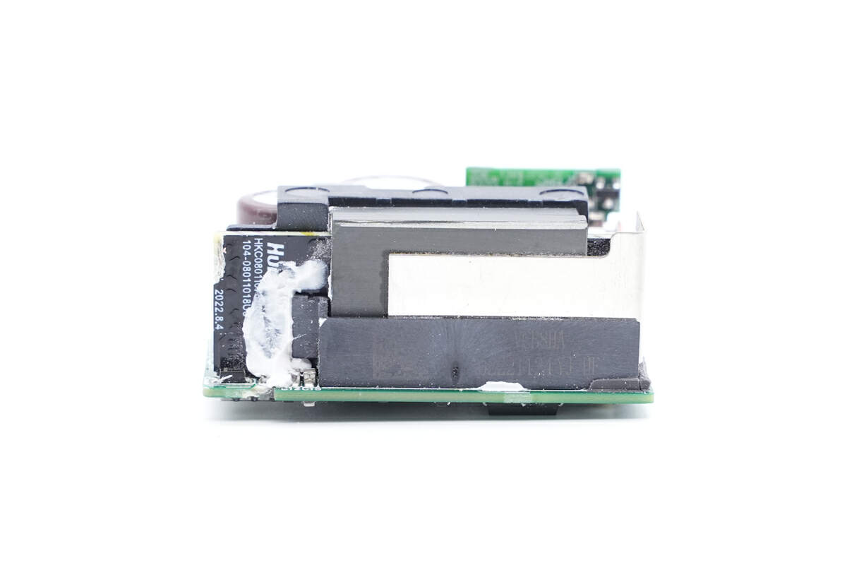
A planar transformer is soldered on the side of the PCBA module. Its magnetic core is insulated by a plastic case.
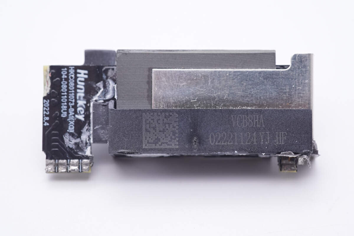
Remove the planar transformer, the magnetic core has a metal sheet to dissipate heat.
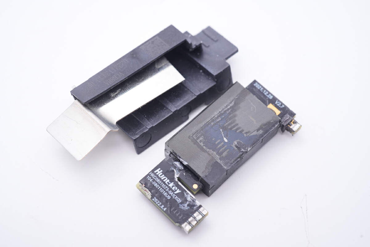
Then remove the plastic case and metal sheet covering the surface of the magnetic core.
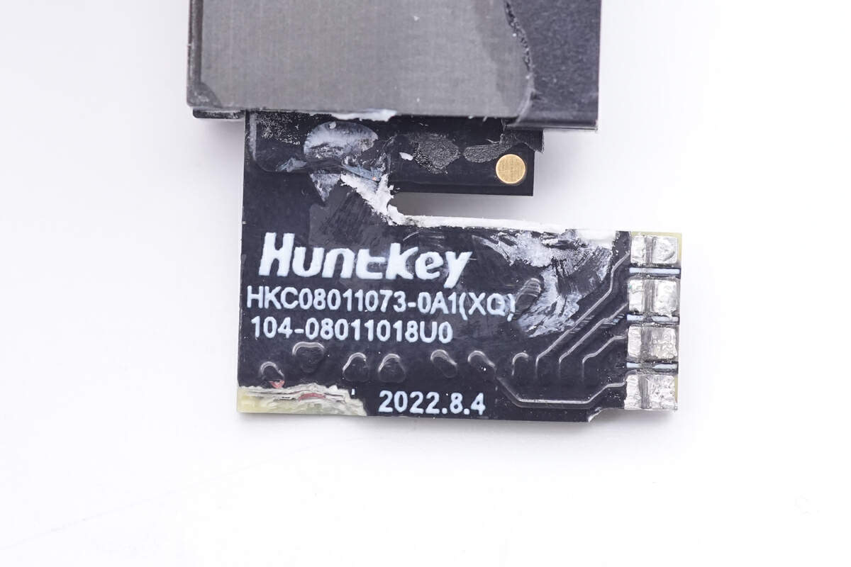
We can see that the planar transformer is from Huntkey.
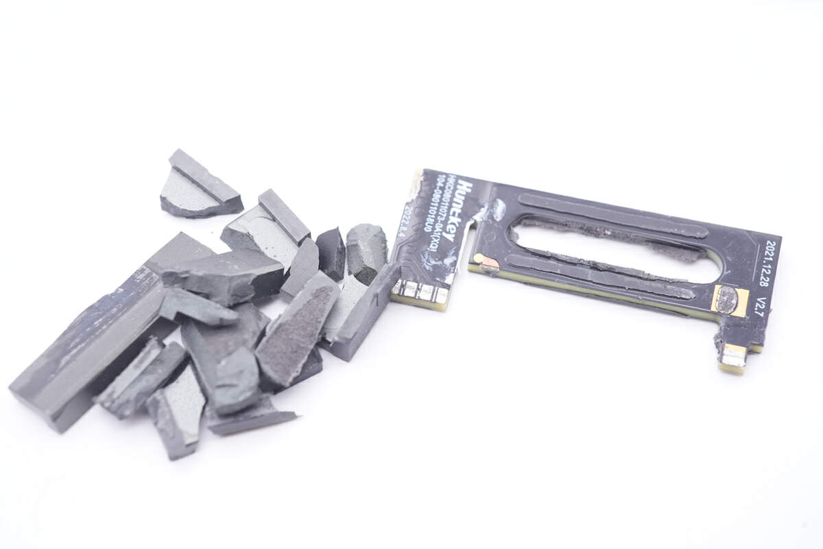
Smash the magnetic core.
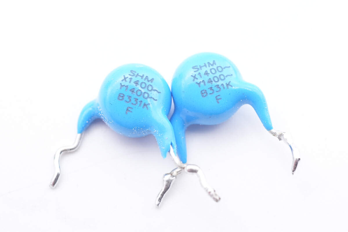
Those two blue Y capacitors are connected in series to increase the withstand voltage, from South HongMing.
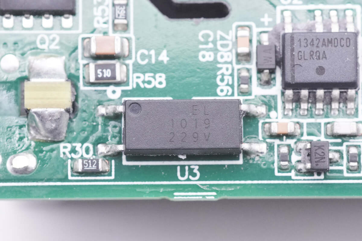
The EL1019 optocoupler is used to regulate the output voltage.
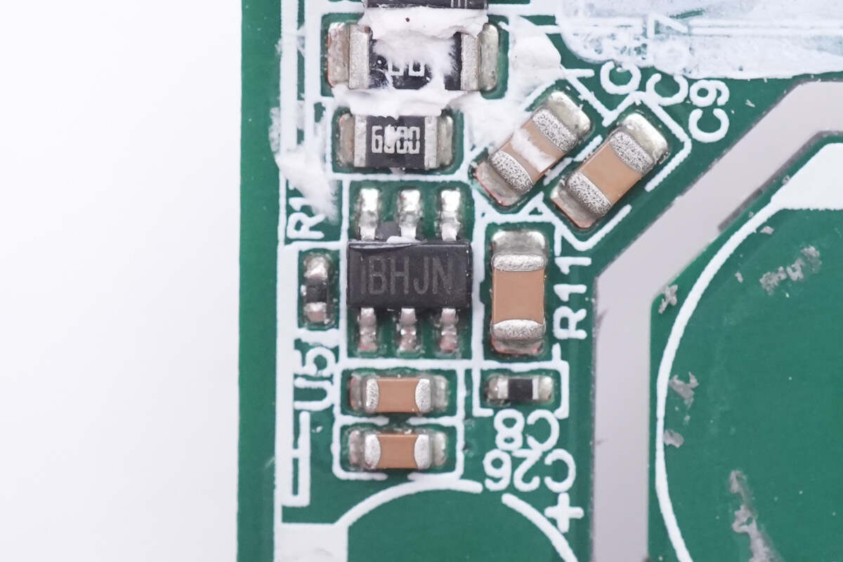
Next, the synchronous rectification circuit.
Its controller is from MPS. Model is MP6908A. And the maximum operating frequency is 600KHz.
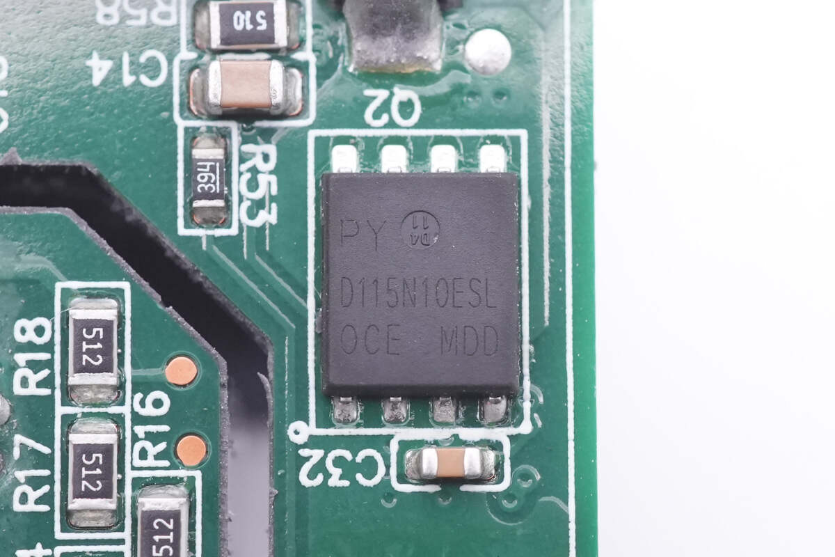
The synchronous rectifier marked with D115N10ESL is from Pingwei and adopts DFN5 x 6 package.
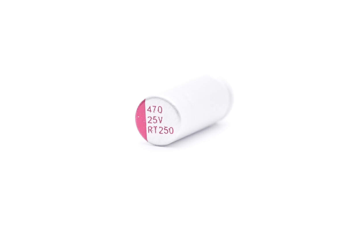
Two solid capacitors for output filtering are from PolyCap, this one is from RT series.

And the other one is from RS series. Both are 470μF 25V.
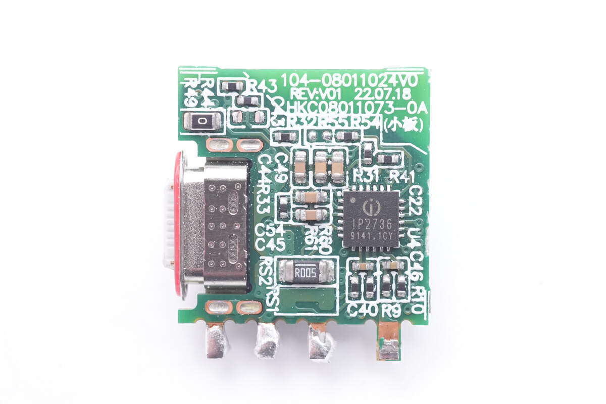
The protocol chip and current sampling resistor are on the front of this output small PCB.
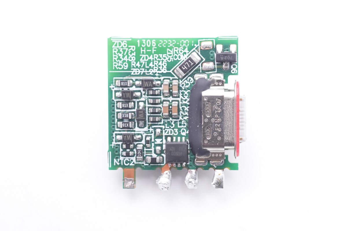
And VBUS MOSFET, thermistor are on the back.
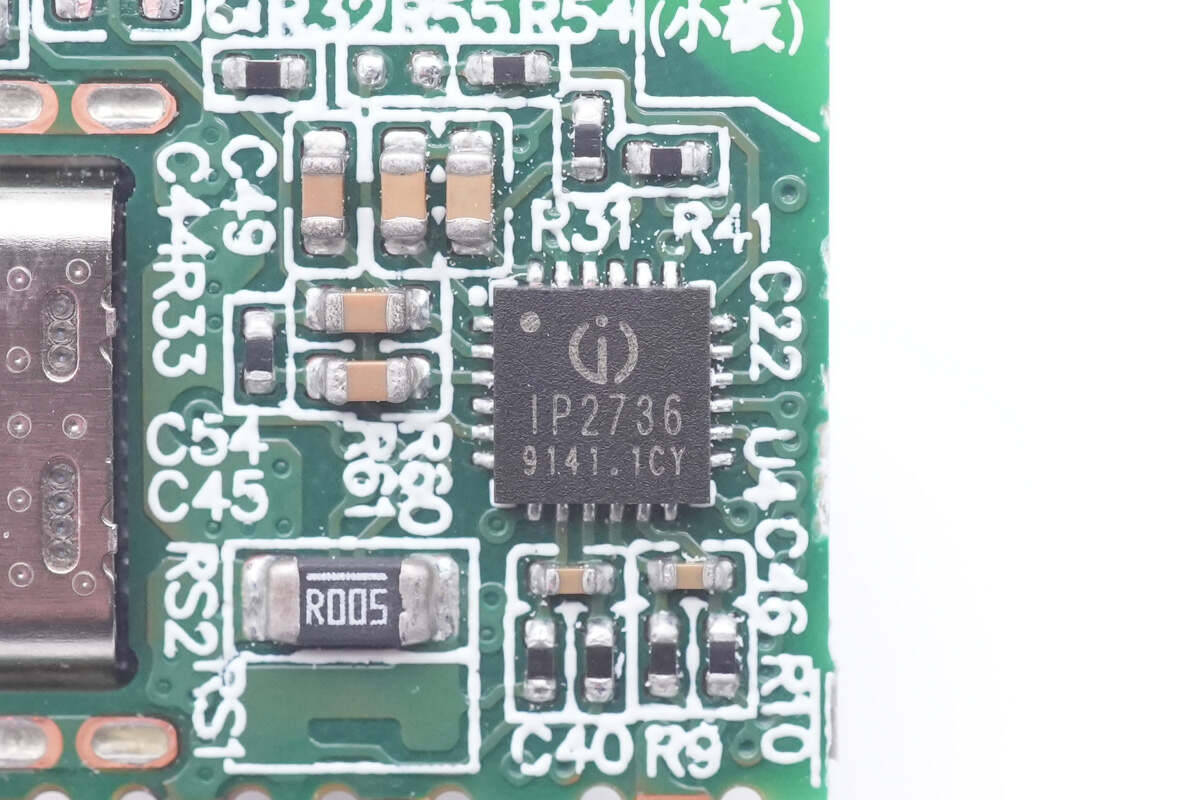
This Injoinic IP2736 protocol chip integrates voltage reference, programmable voltage/current loop control, low-side current detection, and line loss compensation. It also supports optocoupler feedback for power adapter, changes the output voltage through DC-DC controlled by I2C and FB, and is suitable for applications such as car chargers, portable power stations, chargers, power banks, and electric tools.
Thanks to the support of multiple feedback forms, IP2736 can be used with switching power supplies with QR, ACF, LLC and other circuit structures for PD fast charging, and can also be used with high-power car chargers and power banks with buck-boost circuits and other applications.
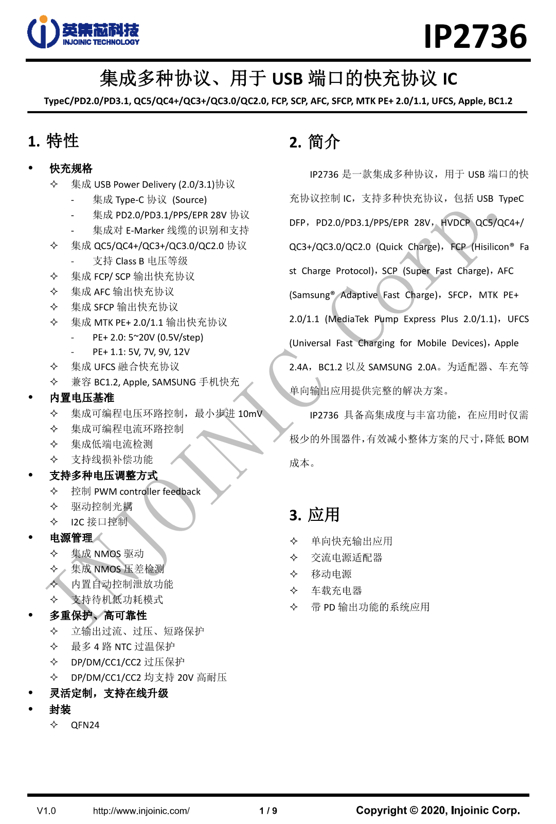
Here is all the information about Injoinic IP2736.
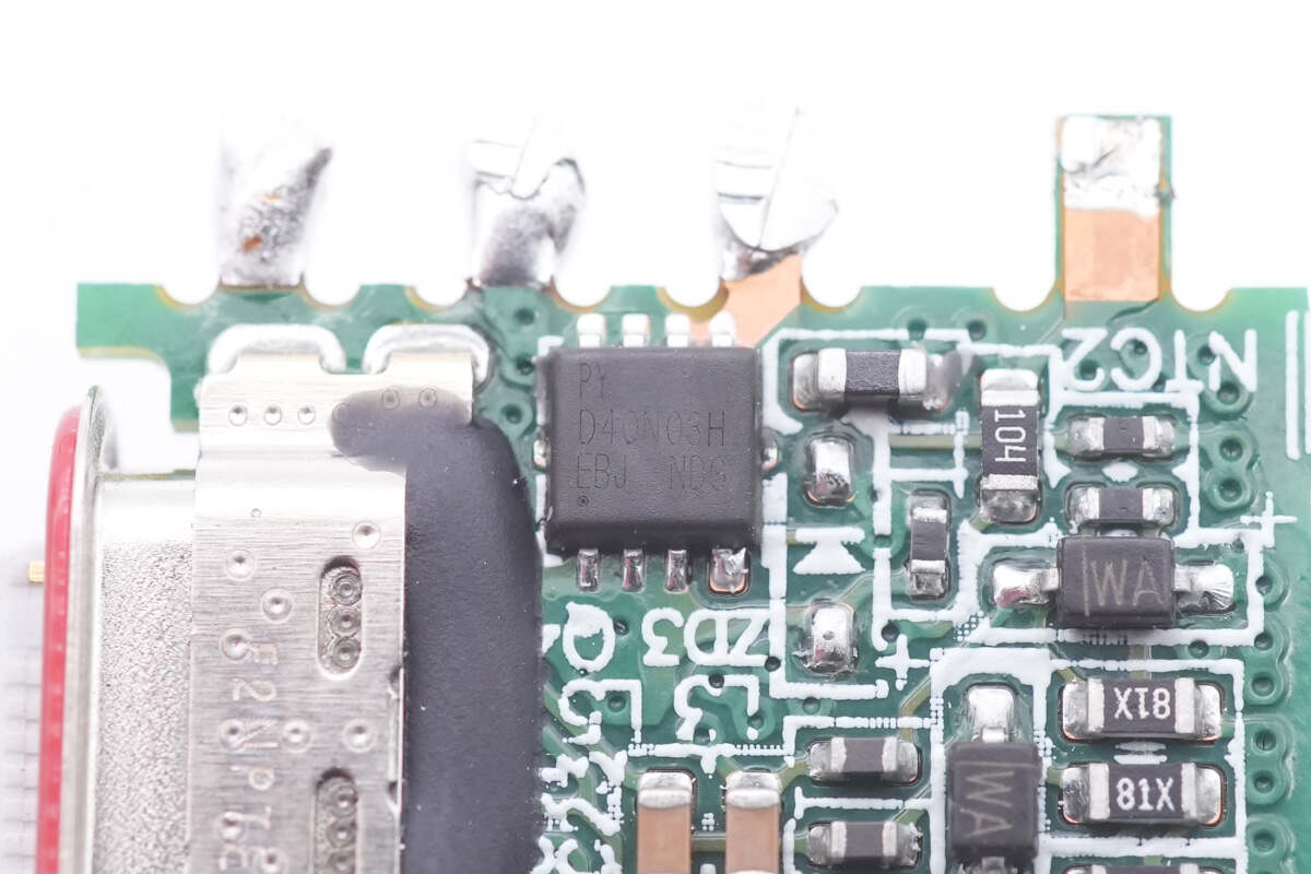
The output VBUS MOSFET is from Pingwei. Model is D40N03H.
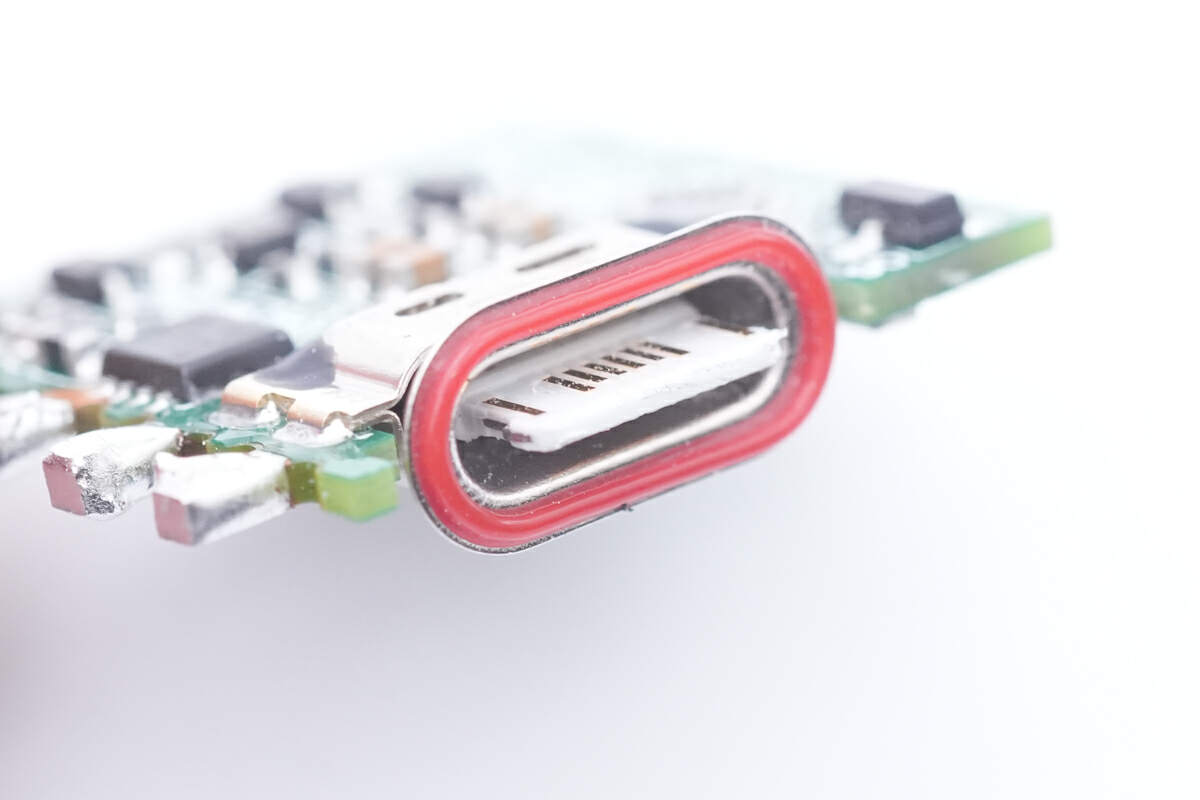
The USB-C connector is fixed on the independent PCB, and the red rubber gasket can be used for dustproof and waterproof.
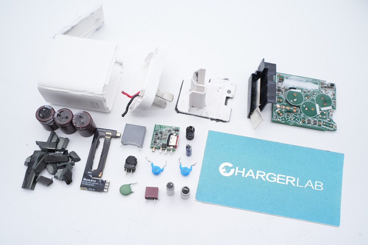
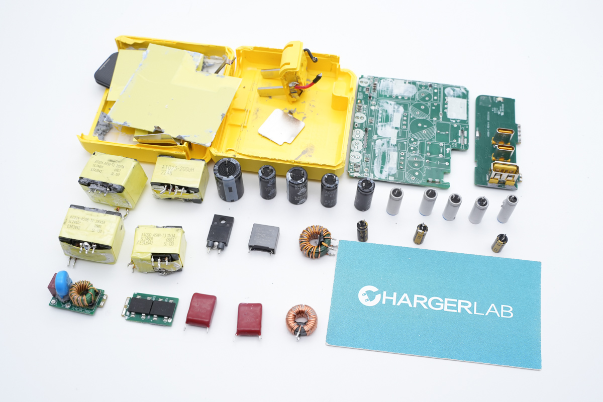
One last look at all the components of this OnePlus 80W SUPERVOOC USB-C Charger.
Summary of ChargerLAB
The OnePlus 80W SUPERVOOC USB-C Charger boasts a sleek white deisgn, a fixed plug design, and a compact form factor. It comes equipped with a USB-C port and supports OPPO's VOOC and SUPERVOOC fast-charging protocols, offering a maximum output power of 80W. Not only does it provide super fast charging for OPPO phones, but it can also serve as a 45W PD charger, able to meet the charging needs of both laptops and smartphones.
After taking it apart, we found it does not have a PFC circuit. The GaN IC and planar transformer can make the charger even smaller. As the default charger of OPPO and OnePlus phones, its quality is comparable to third-party chargers from well-known brands.
Related Articles:
1. Teardown of OnePlus 80W SUPERVOOC USB-C GaN Charger (Video)
2. Charging Review of OnePlus SUPERVOOC 100W Dual Ports Charger
3. Teardown of OPPO 80W SuperVOOC charger (Single USB-A)

