Introduction
ChargerLAB had done multiple tests on the MOVESPEED 140W PD3.1 charger. It can meet the charging needs of most devices. It also supports automatic power distribution and can charge four devices at the same time.
This time, we got its yellow version. To know how it can achieve a charging performance like that, we are going to take it apart to see its internal components and structure.
Product Appearance
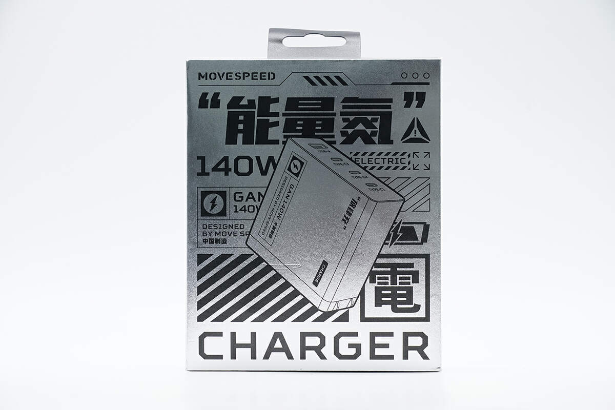
The packaging box adopts a silver glossy design with MOVESPEED printed on the front.
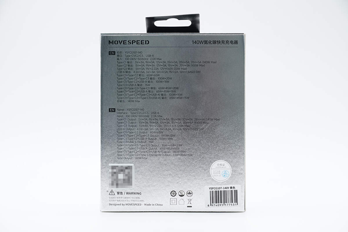
The specs info are printed on the back. We'll talk about later.
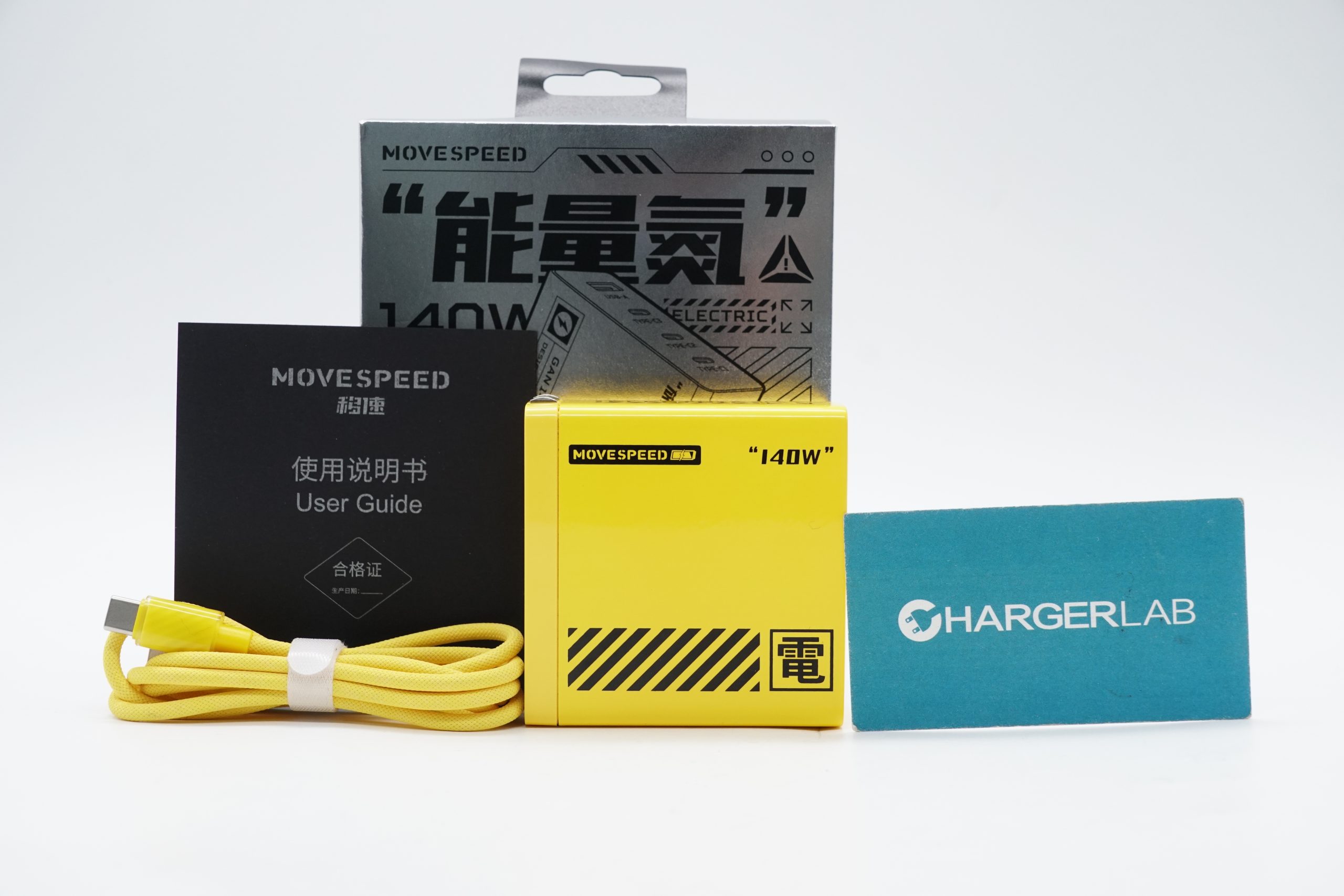
The box contains the charger, a dual USB-C cable, and some documents.
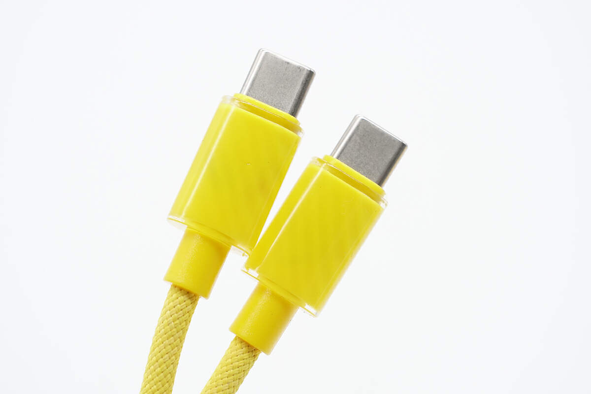
The dual USB-C cable adopts a braided design, and the color is the same as the charger.
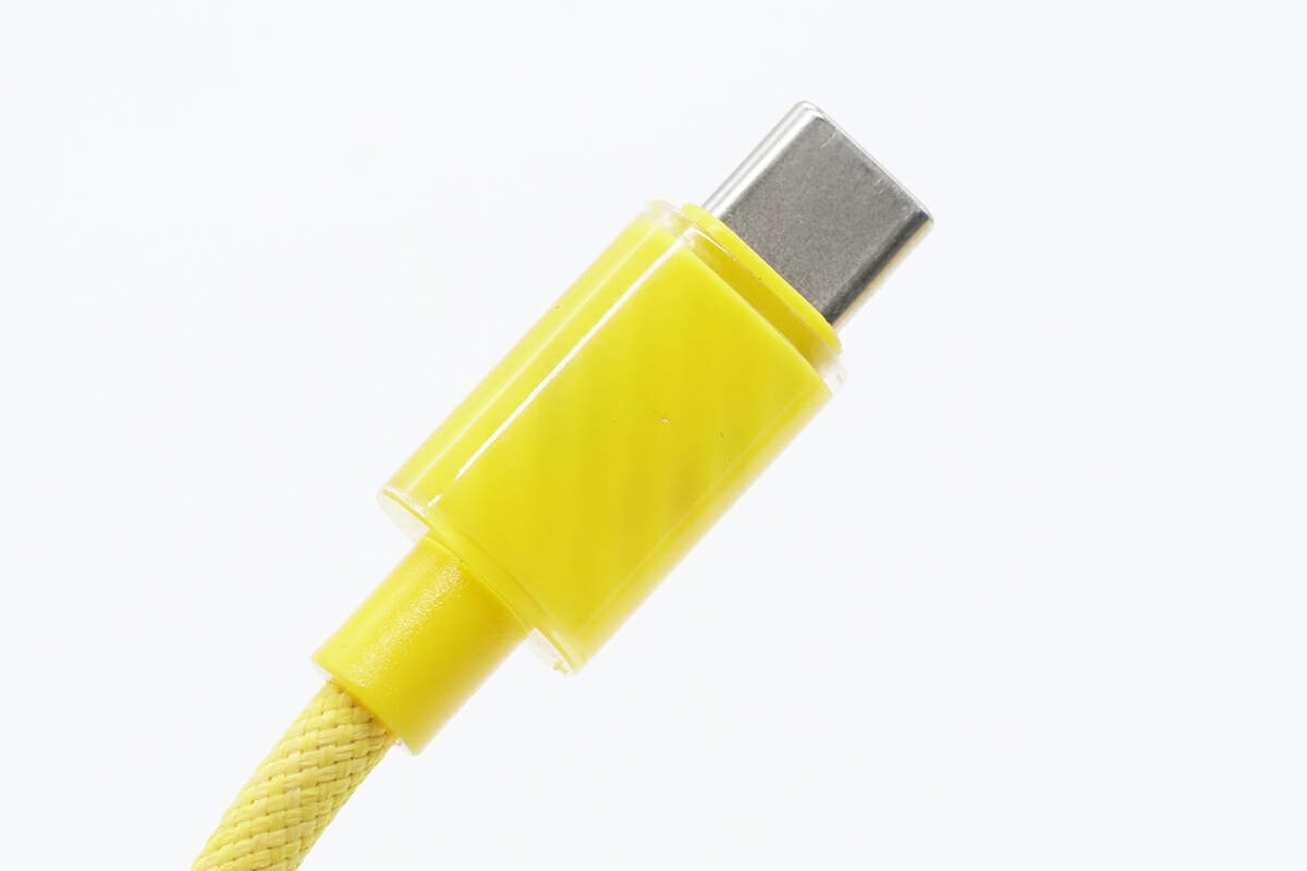
The connector has a double-layer design. The outer layer is made of transparent material, and the inner layer is made of green PC.
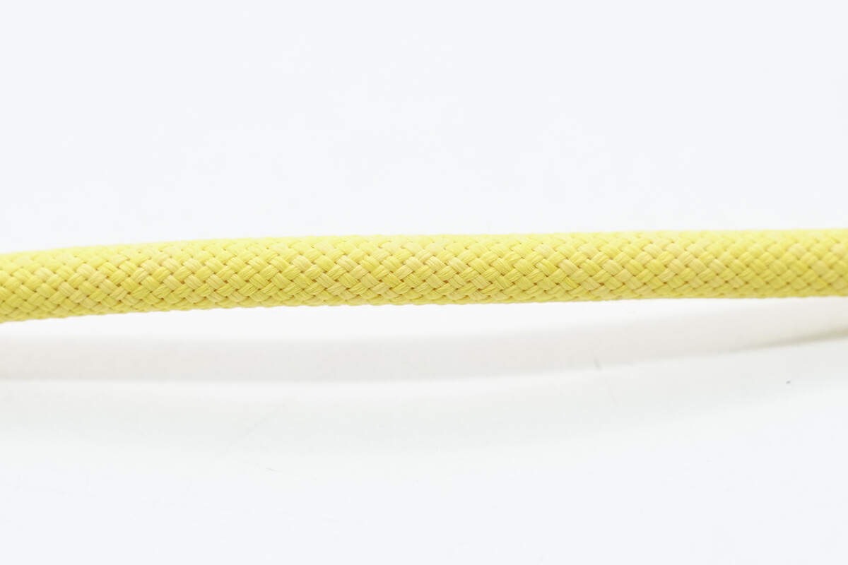
The braided design allows for a longer lifespan.
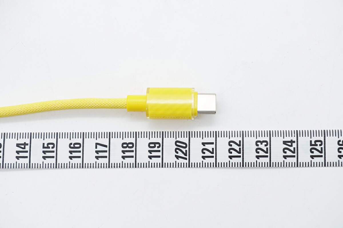
The length of it is about 121 cm (3'97'').
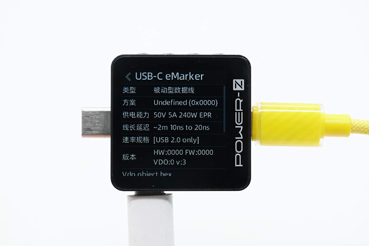
The ChargerLAB POWER-Z KM003C shows it can support 50V5A and has an E-marker chip. It can also support USB 2.0 and PD3.1 240W.
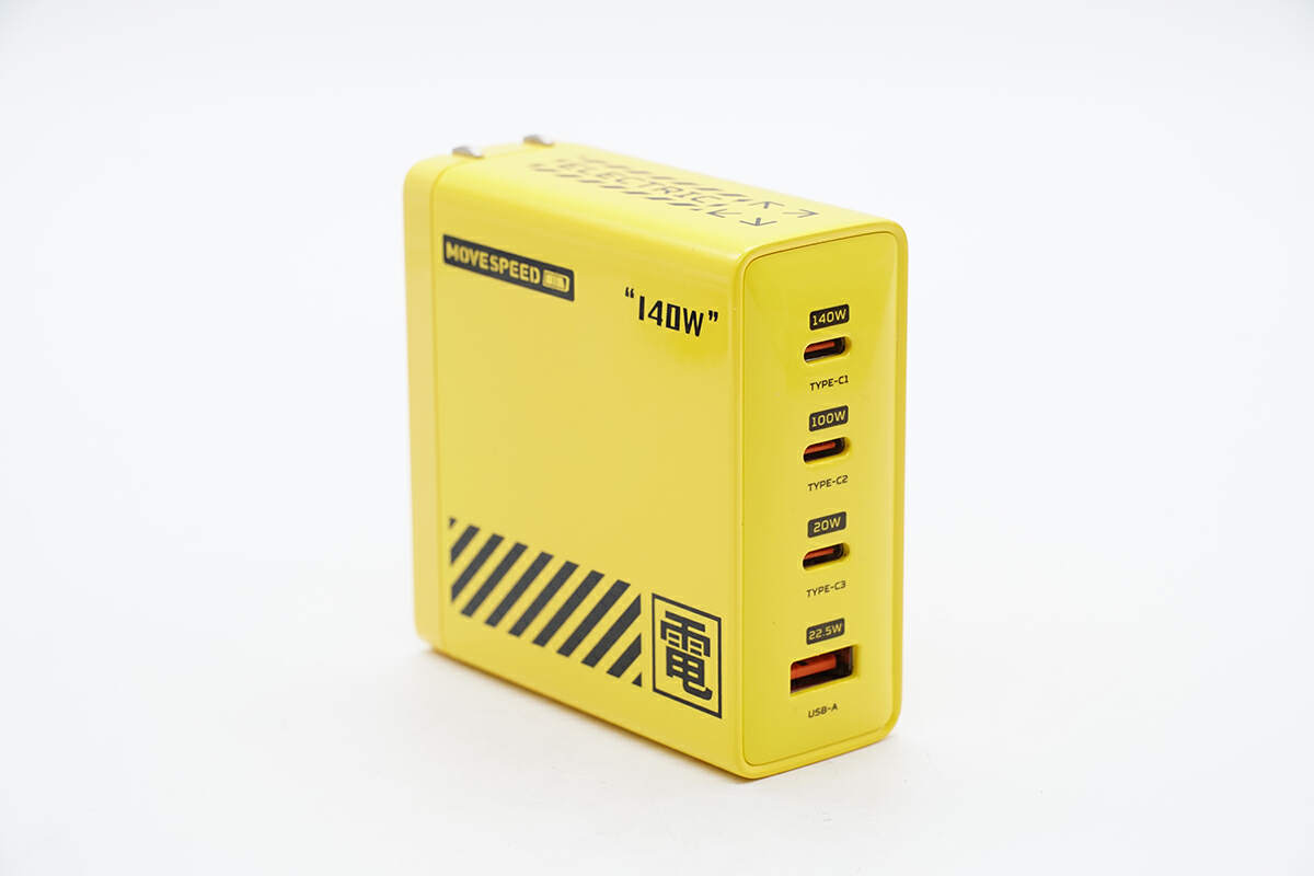
This charger comes in a bright yellow.
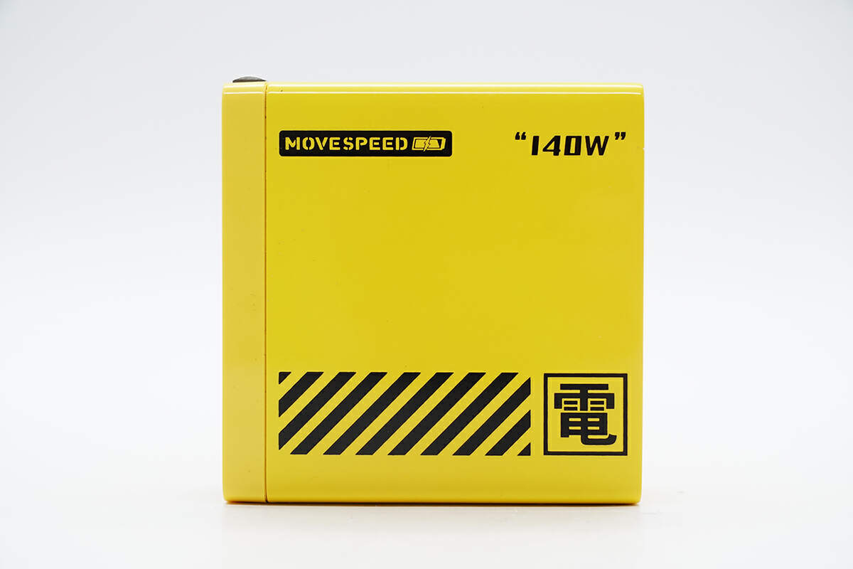
The words "MOVESPEED" and "140W" are printed on the front of it.
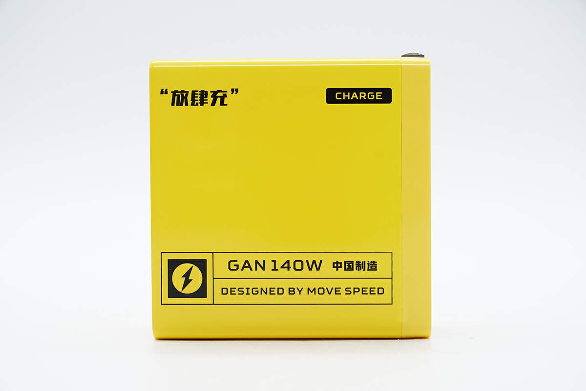
The GAN 140W is printed on the back.
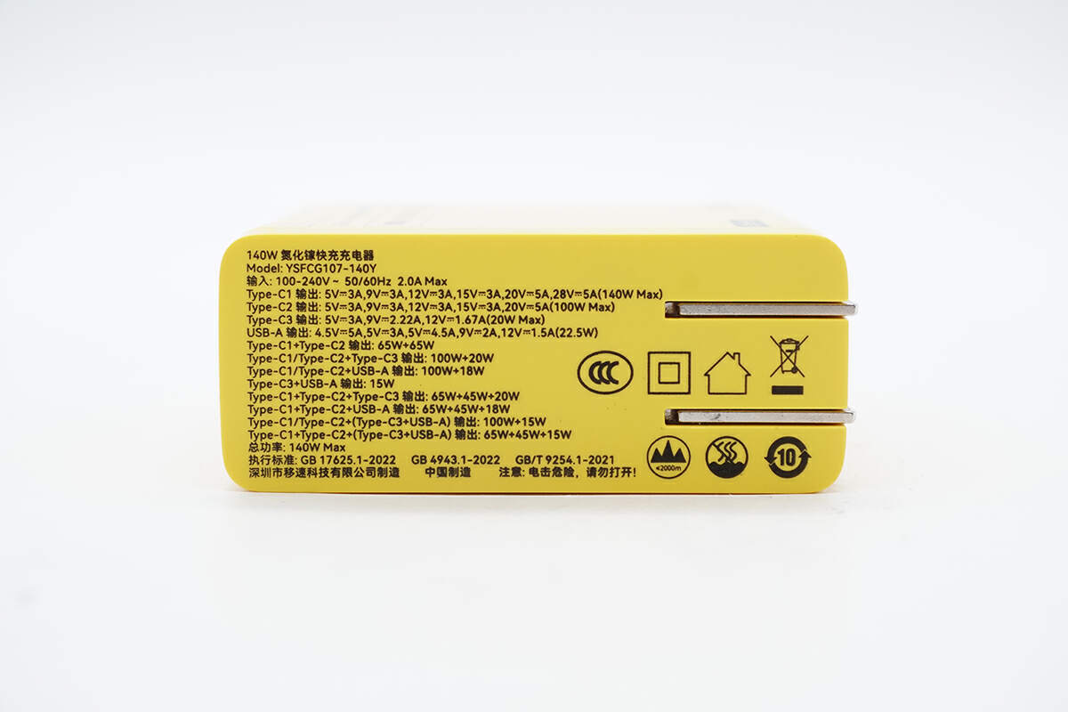
The specs info are also printed on the input panel.
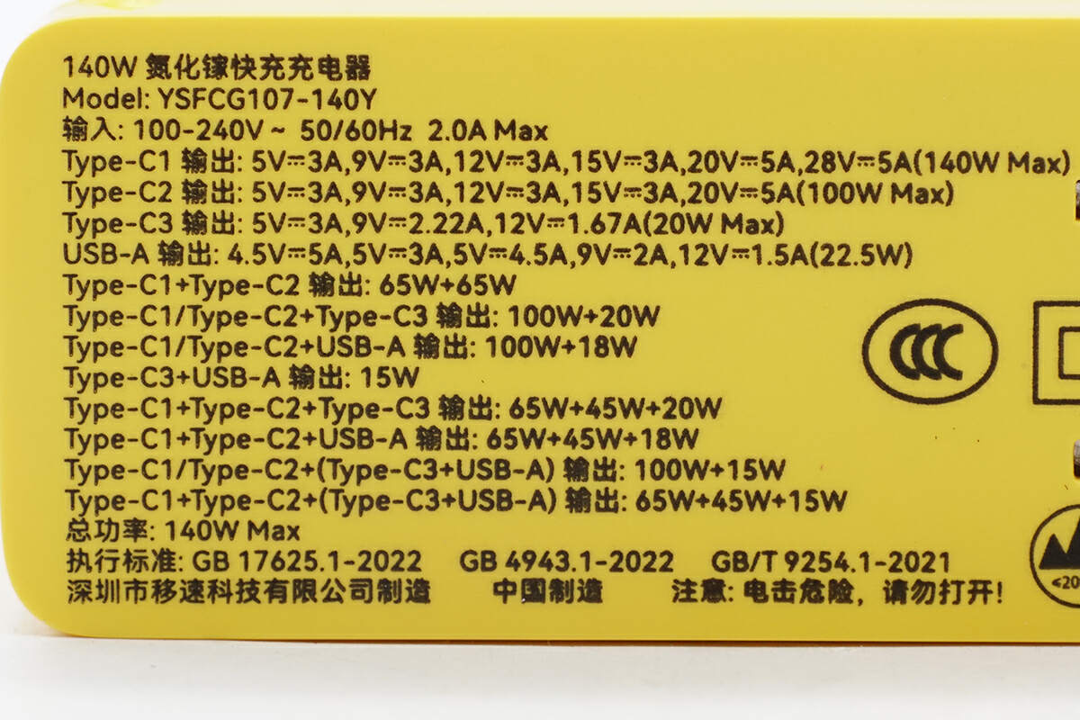
Model is YSFCG107-140Y. It can support input of 100-240V~ 50/60Hz 2.0A. The highest charging power for USB-C1 to USB-A is 140W, 100W, 20W, 22.5W, respectively. And the total charging power can reach 140W.
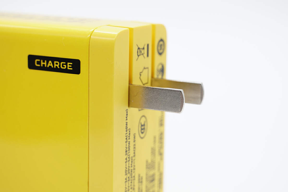
Here are the foldable prongs.
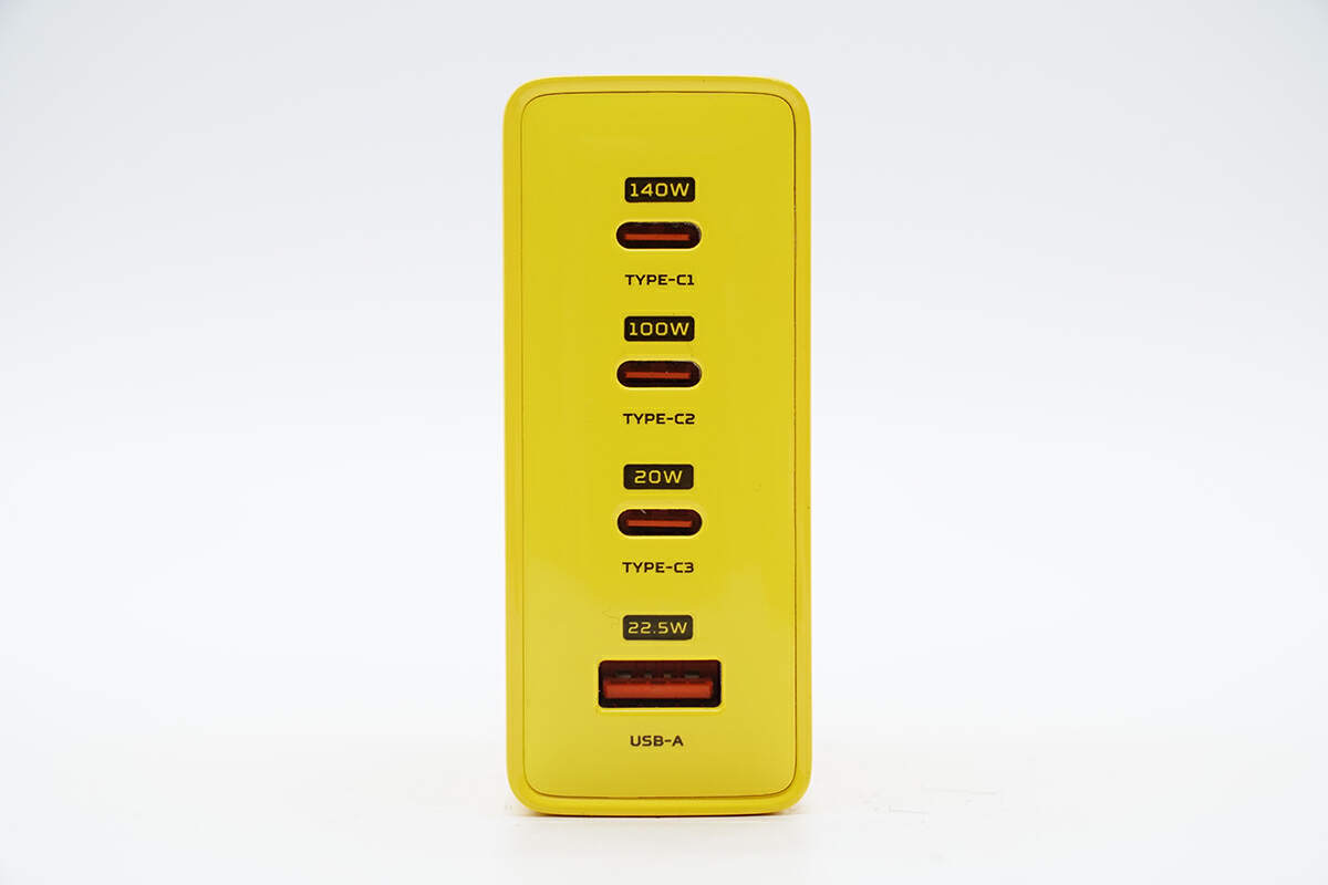
There are four output ports. The output panel shows the maximum output power of each port.
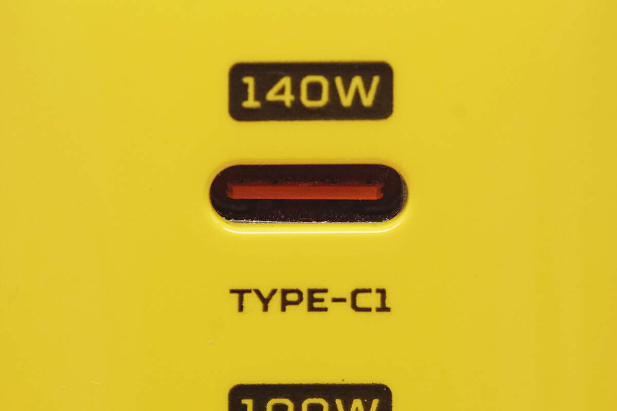
The four ports are all orange.
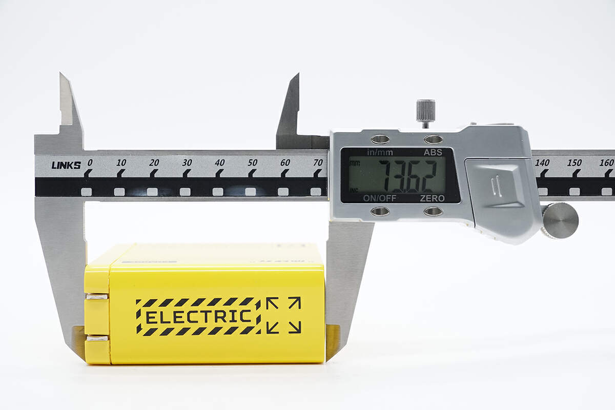
The length of the charger is about 74 mm (2.91 inches).
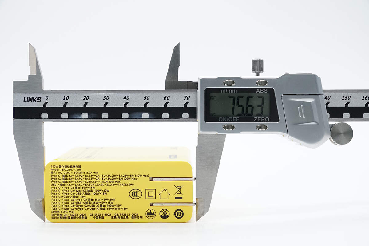
The width is about 76 mm (2.99 inches).
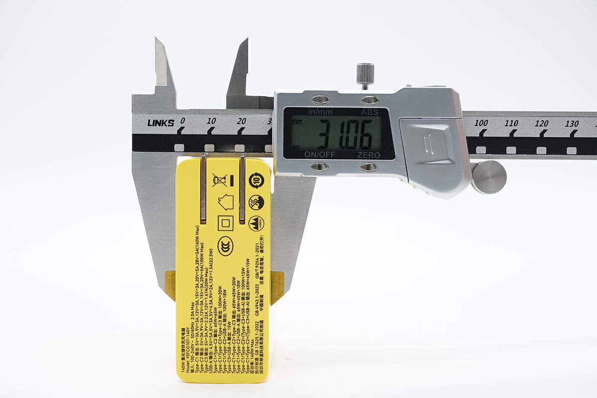
The thickness is about 31 mm (1.22 inches).
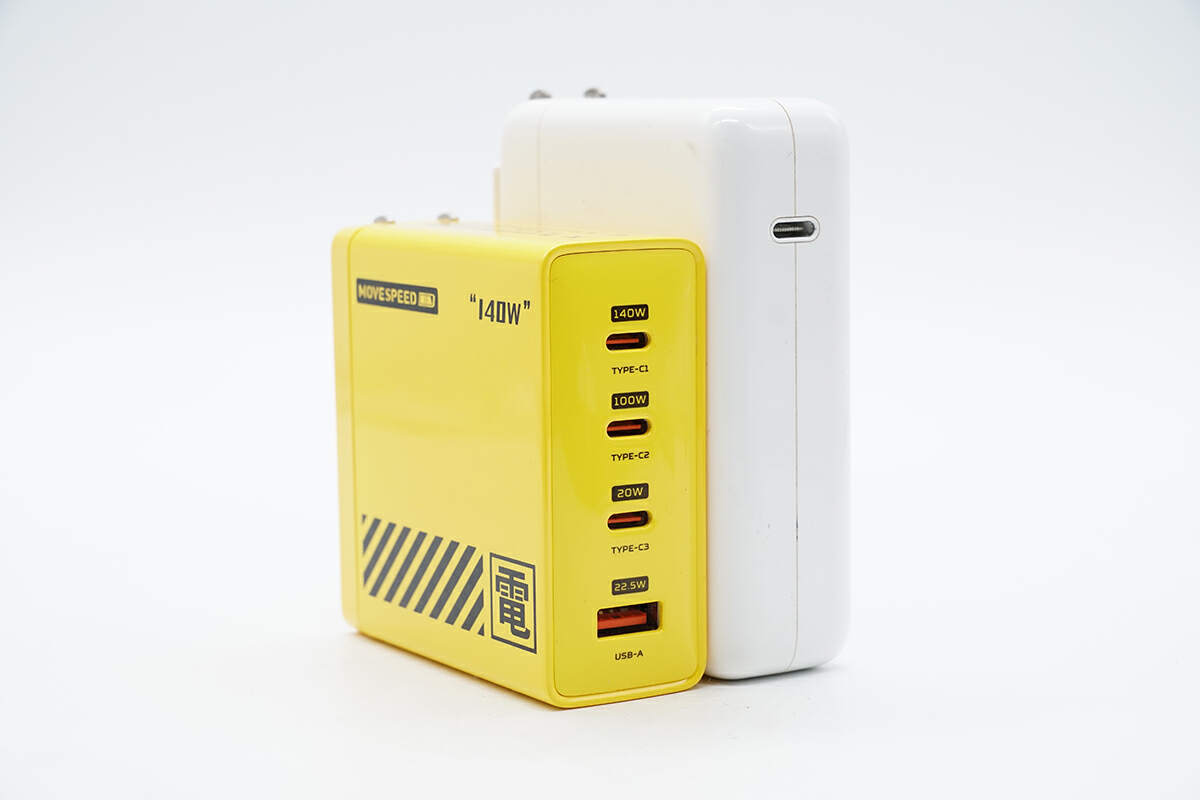
Even though it has four ports, it is still smaller than the Apple 140W charger.
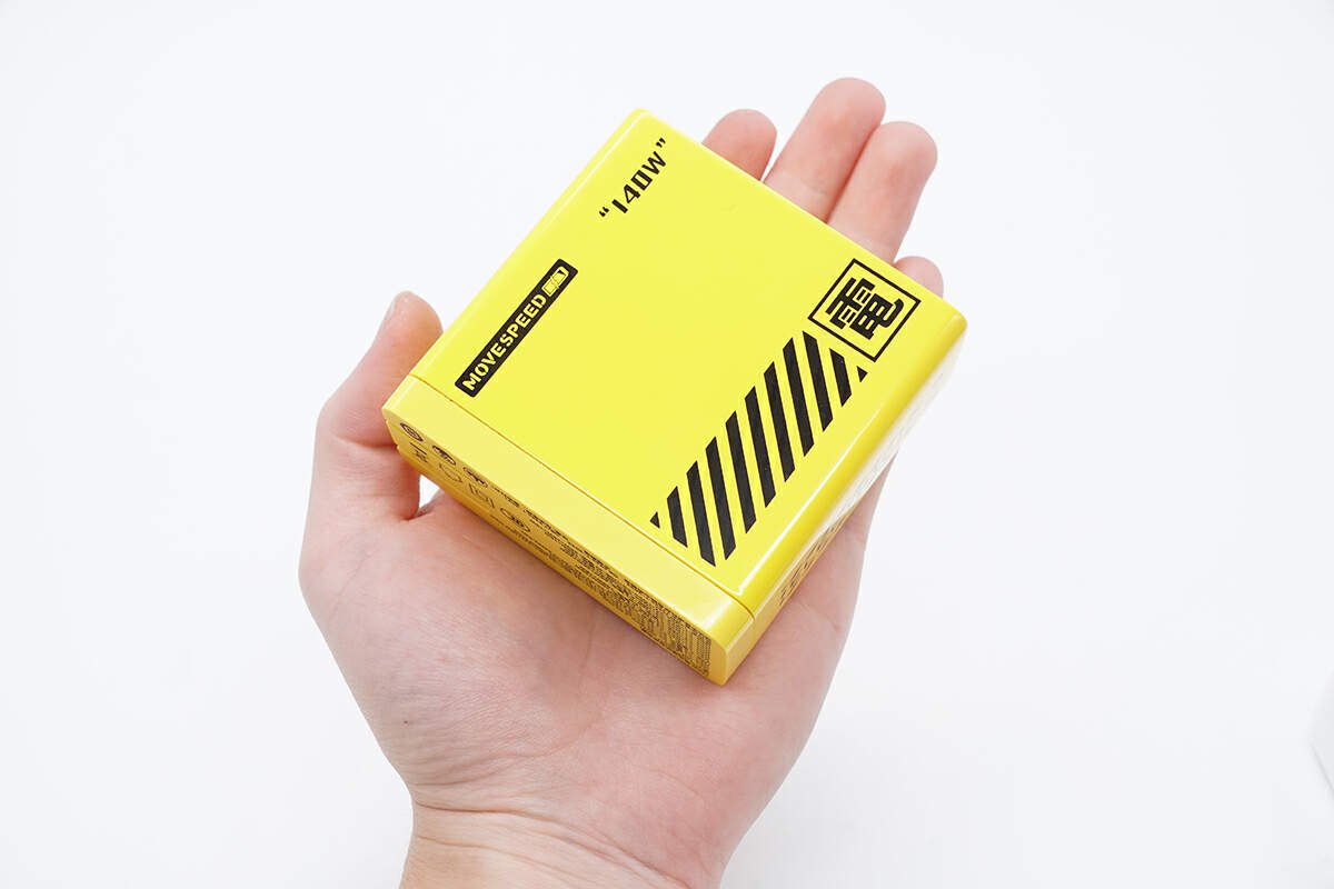
That's how big it is in the hand.
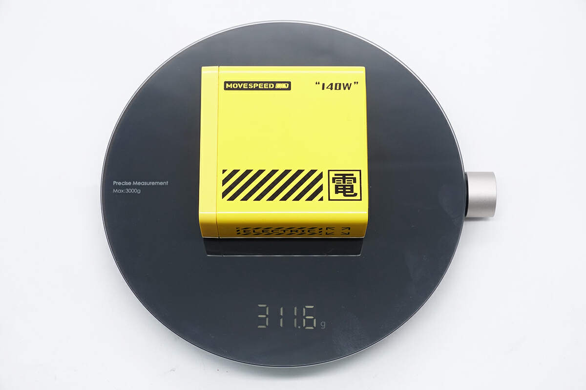
The weight is about 312 g (11 oz).
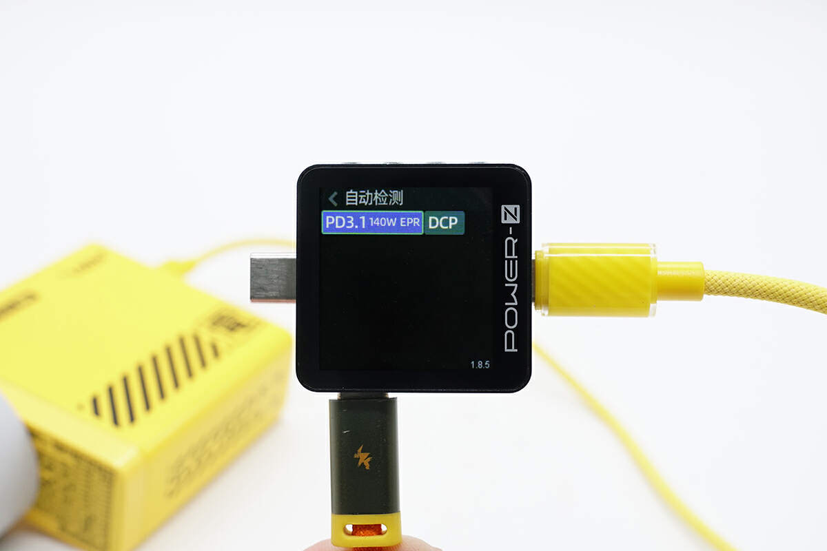
ChargerLAB POWER-Z KM003C shows the USB-C1 port can support PD3.1 and DCP charging protocols.
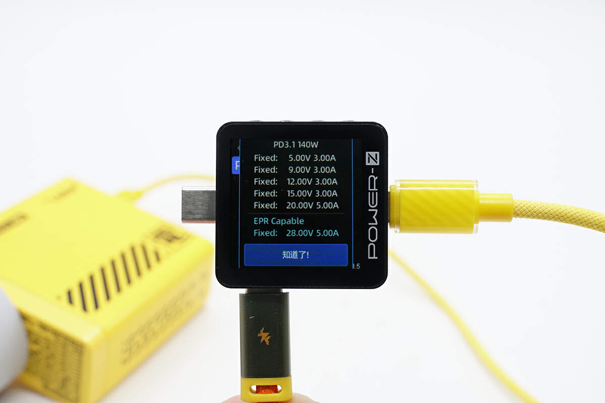
And it has six fixed PDOs of 5V3A, 9V3A, 12V3A, 15V3A, 20V5A, and 28V/5A.
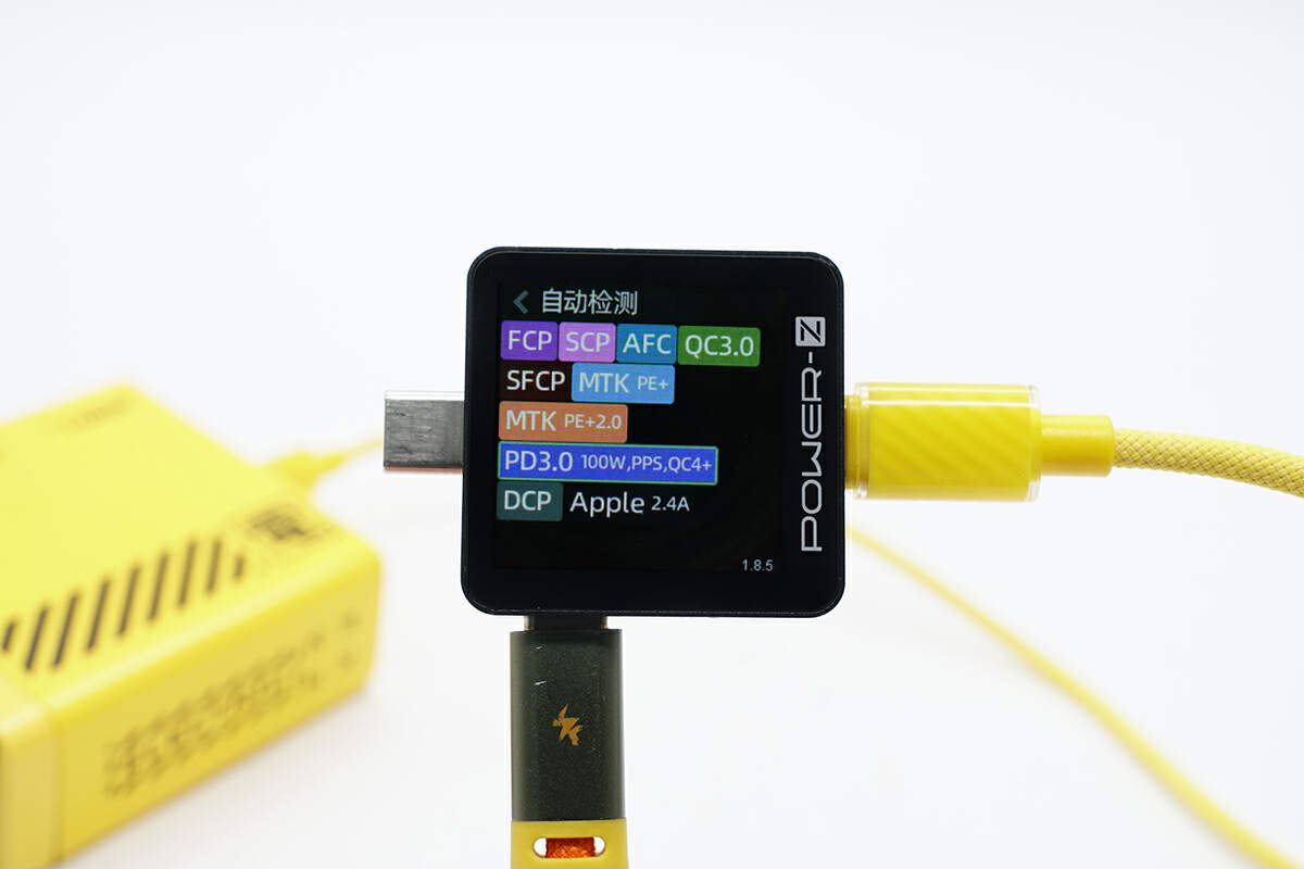
ChargerLAB POWER-Z KM003C shows the USB-C2 port can support FCP, SCP, AFC, QC3.0, QC4+, SFCP, PE2.0, PD3.0, PPS, DCP, and Apple 2.4A charging protocols.
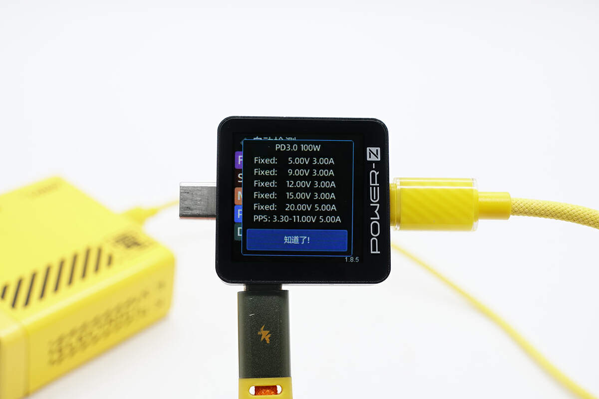
And it has five fixed PDOs of 5V3A, 9V3A, 12V3A, 15V3A, 20V5A, and a set of PPS, which is 3.3-11V/5A.
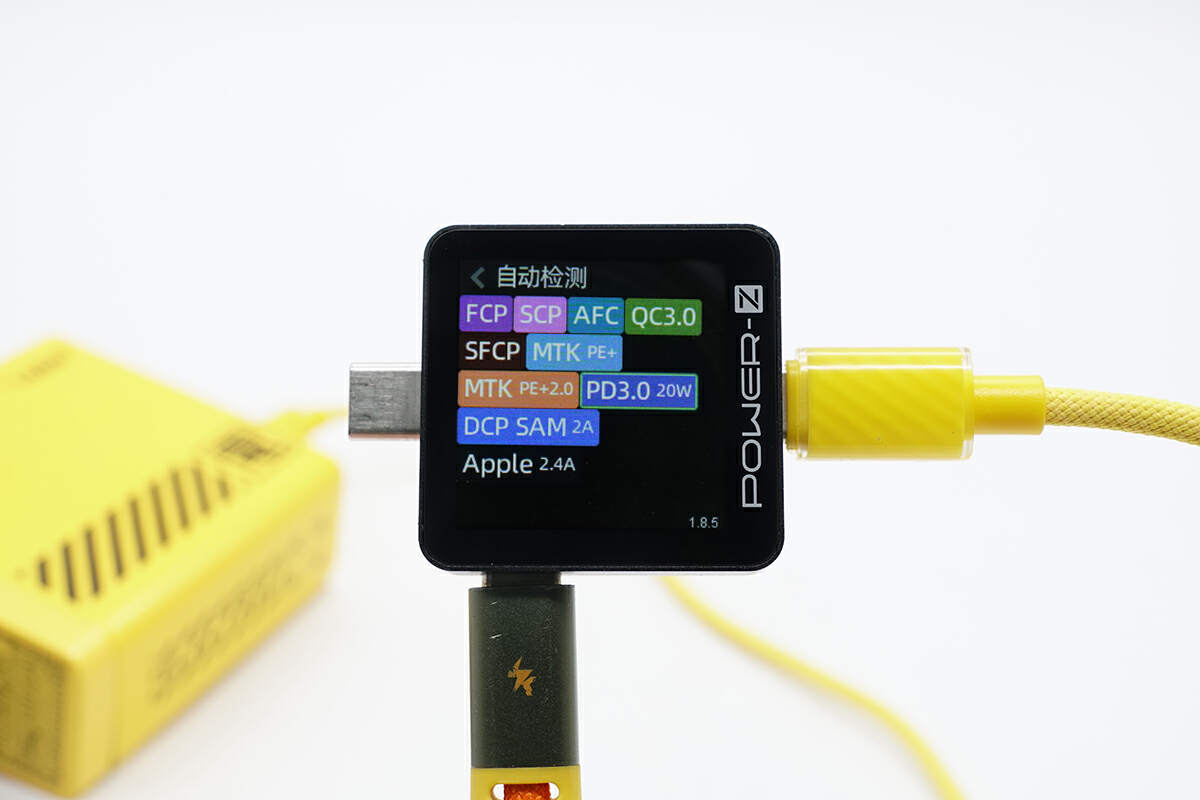
ChargerLAB POWER-Z KM003C shows the USB-C3 port can support FCP, SCP, AFC, QC3.0, SFCP, PE2.0, PD3.0, DCP, SAM 2A, and Apple 2.4A charging protocols.
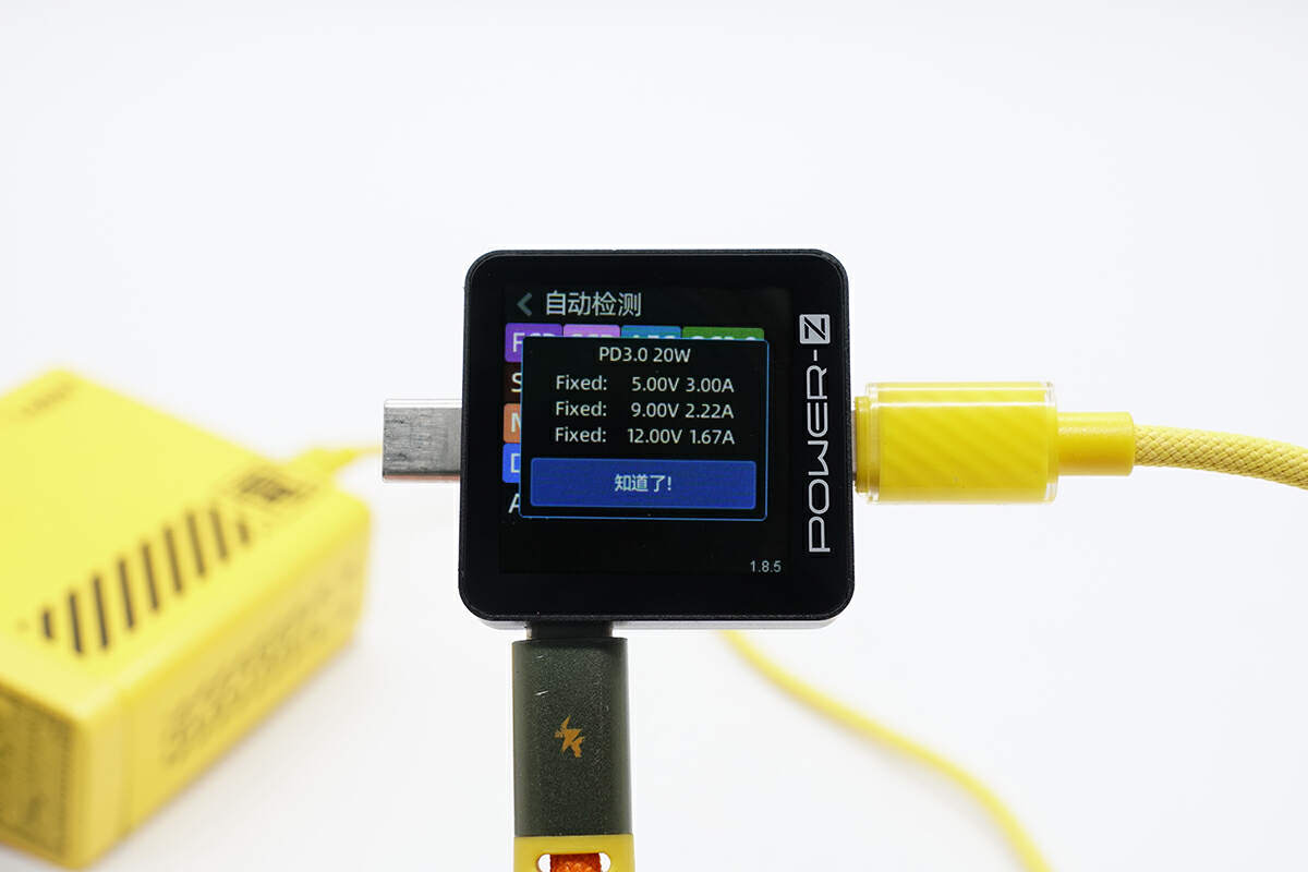
And it has three fixed PDOs of 5V3A, 9V/2.22A, and 12V/1.67A.
The USB-A port can support FCP, SCP, AFC, QC3.0, SFCP, PE2.0, DCP, SAM 2A, and Apple 2.4A charging protocols.
Teardown
After the product's appearance, let's start to take it apart.
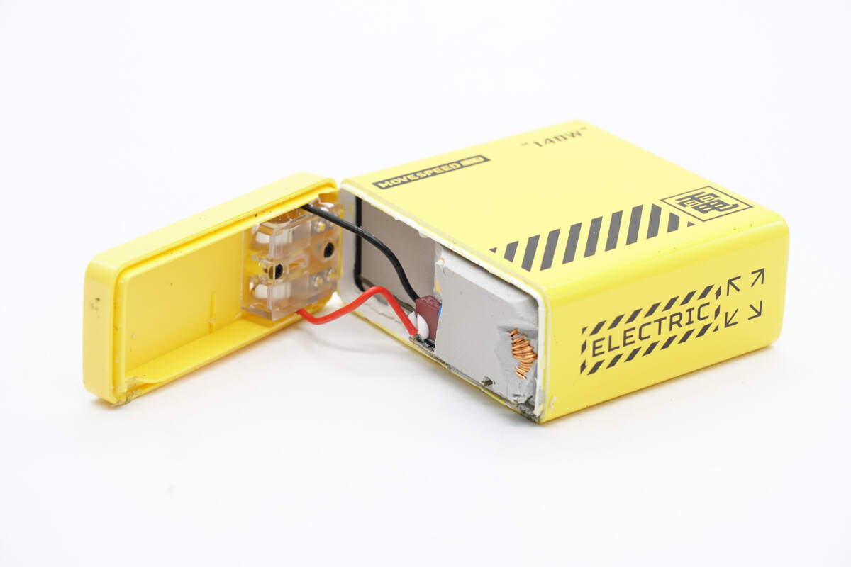
Remove the cover along the gap. The PCBA module and the prongs are connected by wires.
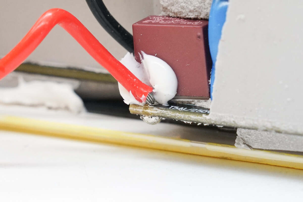
The wires are soldered to the PCBA module.
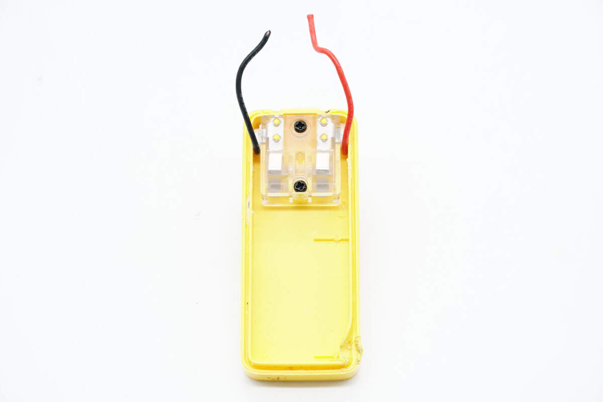
The foldable prongs are fixed with screws.
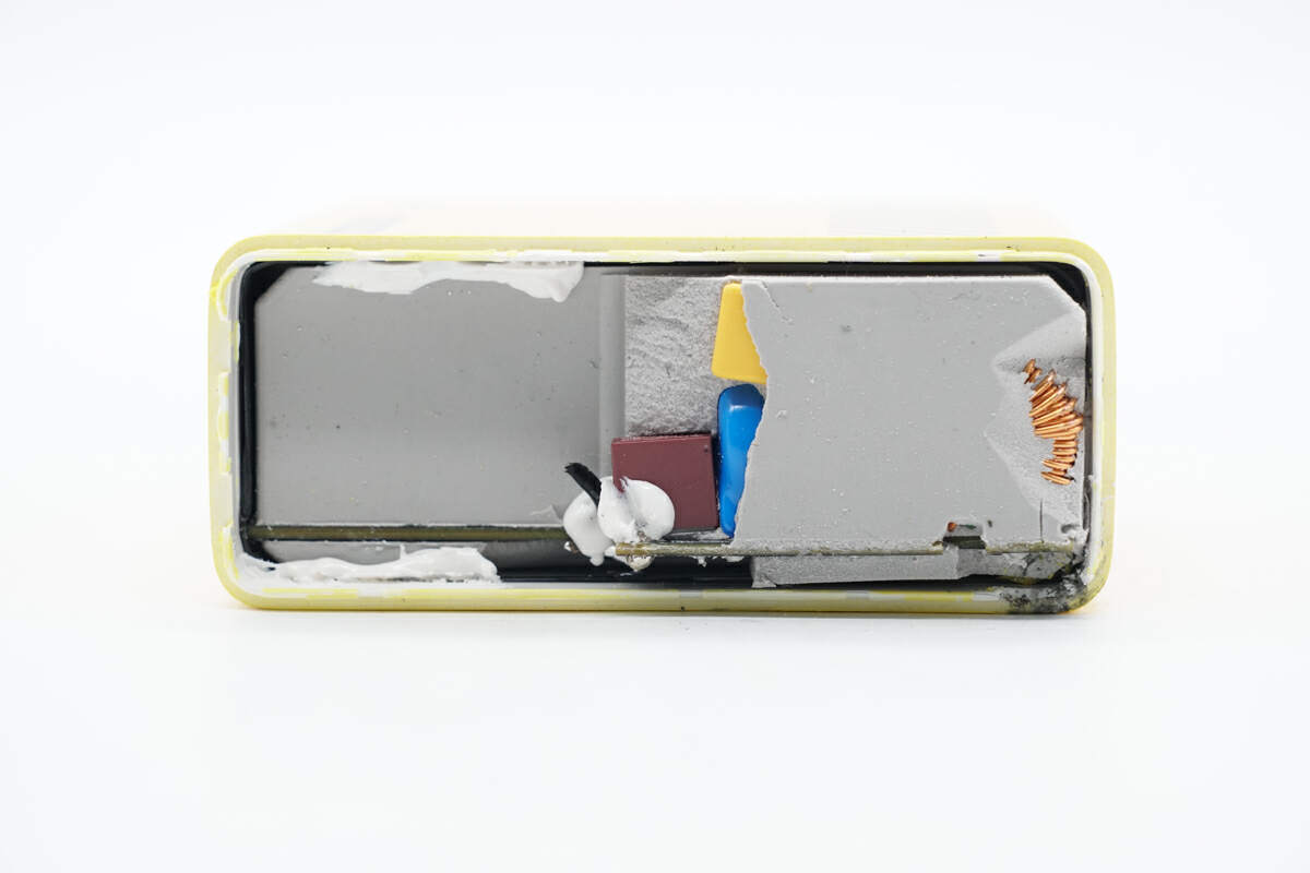
The PCBA module is filled with potting compound.
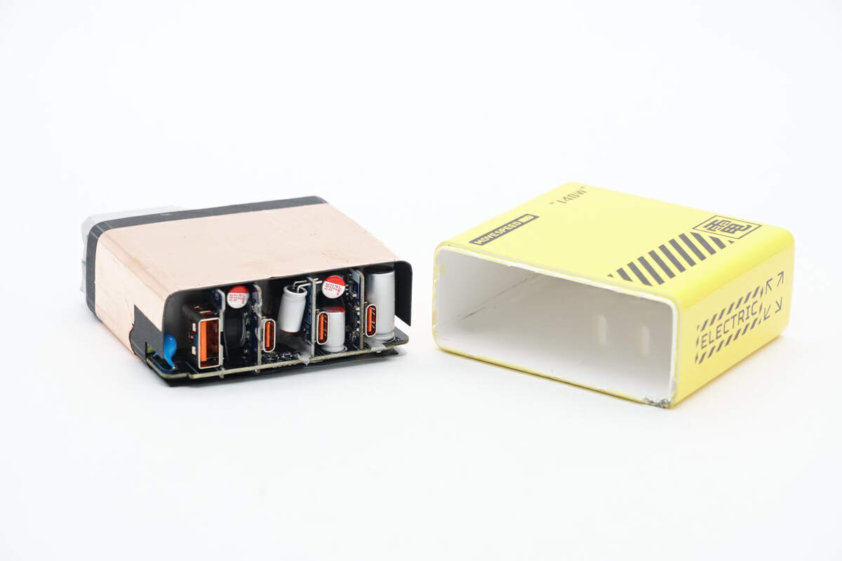
Take out the PCBA module from the case.
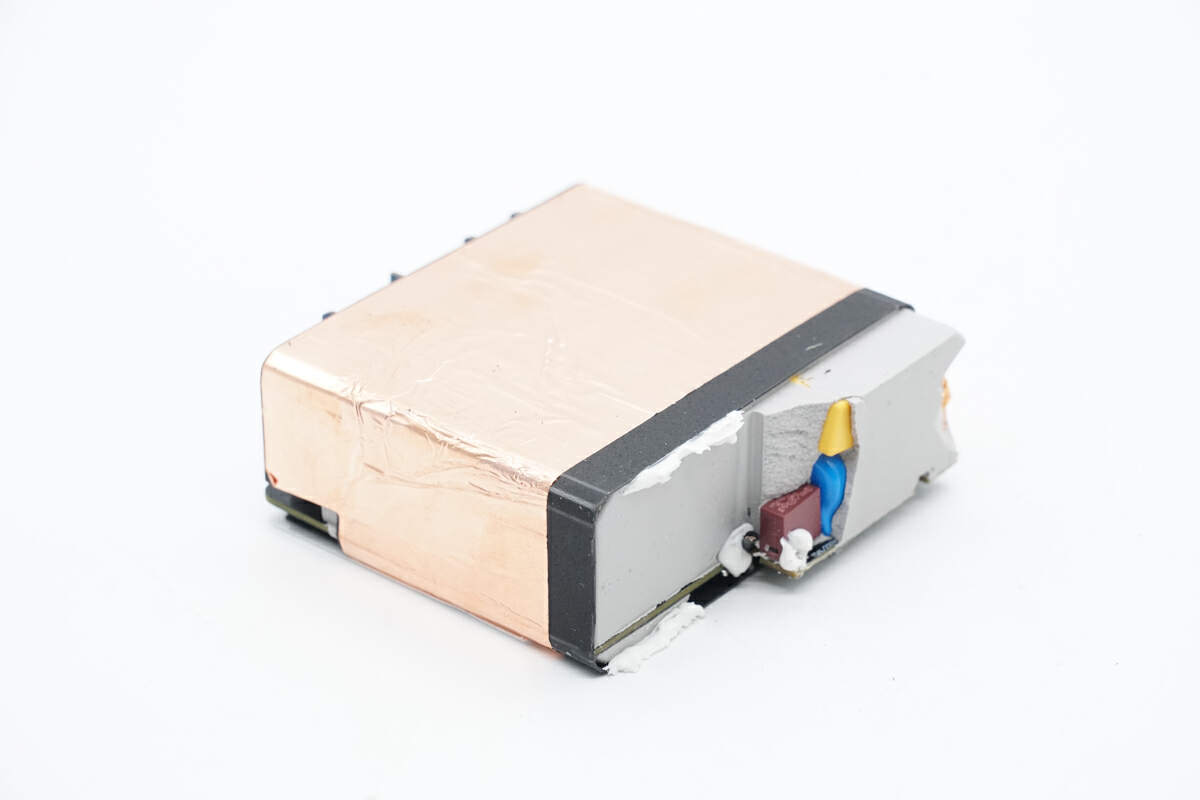
The PCBA module is wrapped and insulated with mylar sheets. And there is the copper sheet on the outside of the mylar sheets for shielding.
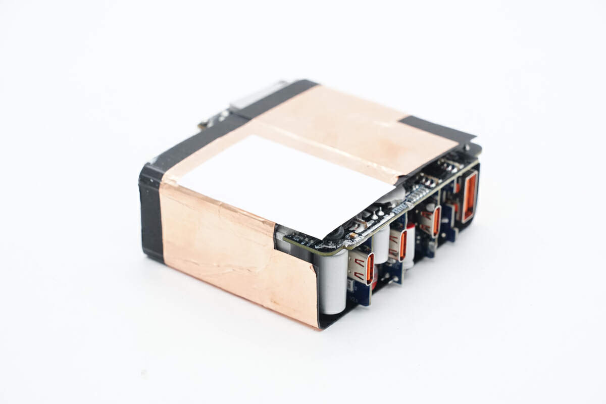
The back of the PCBA module is also covered with heat sinks.
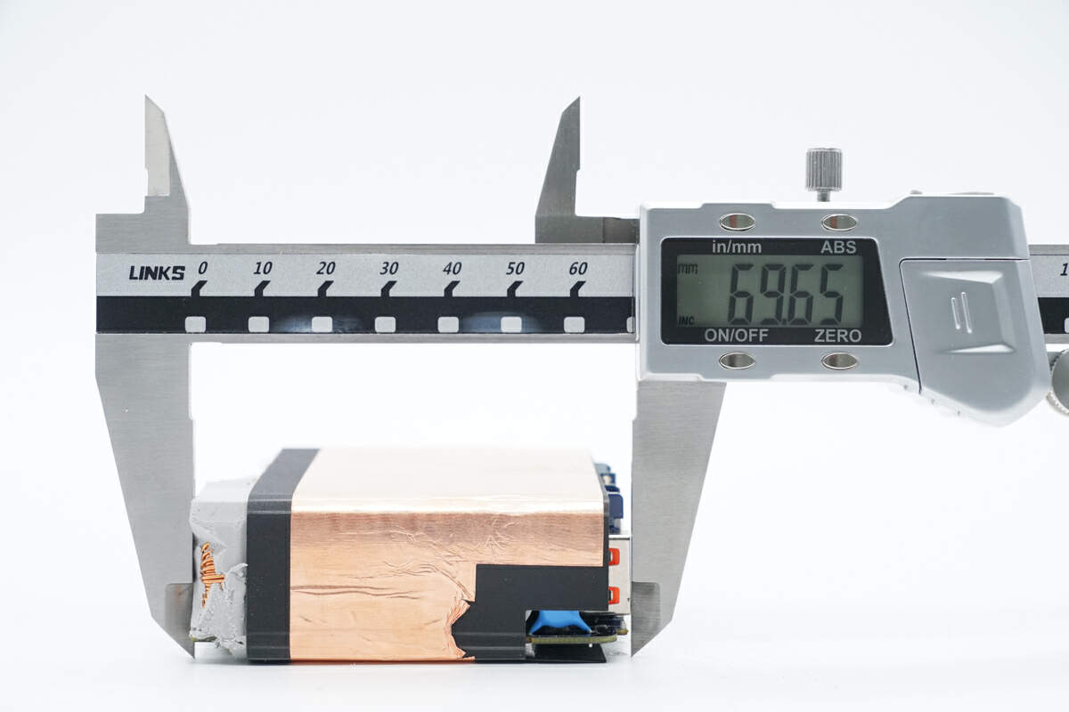
The length of the PCBA module is about 70 mm (2.76 inches).
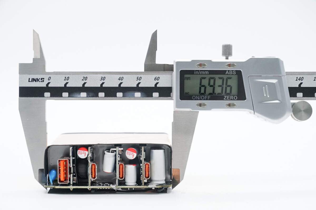
The width is also about 70 mm (2.76 inches).
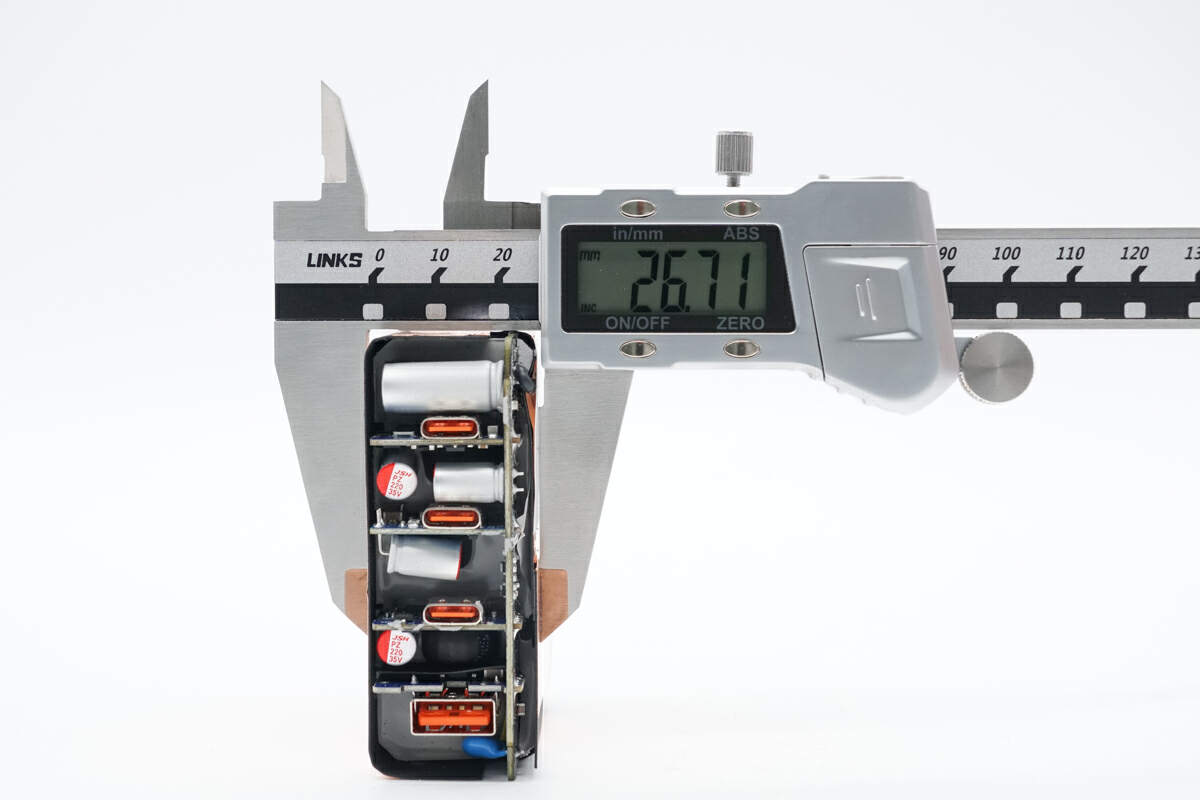
The thickness is about 27 mm (1.06 inches).
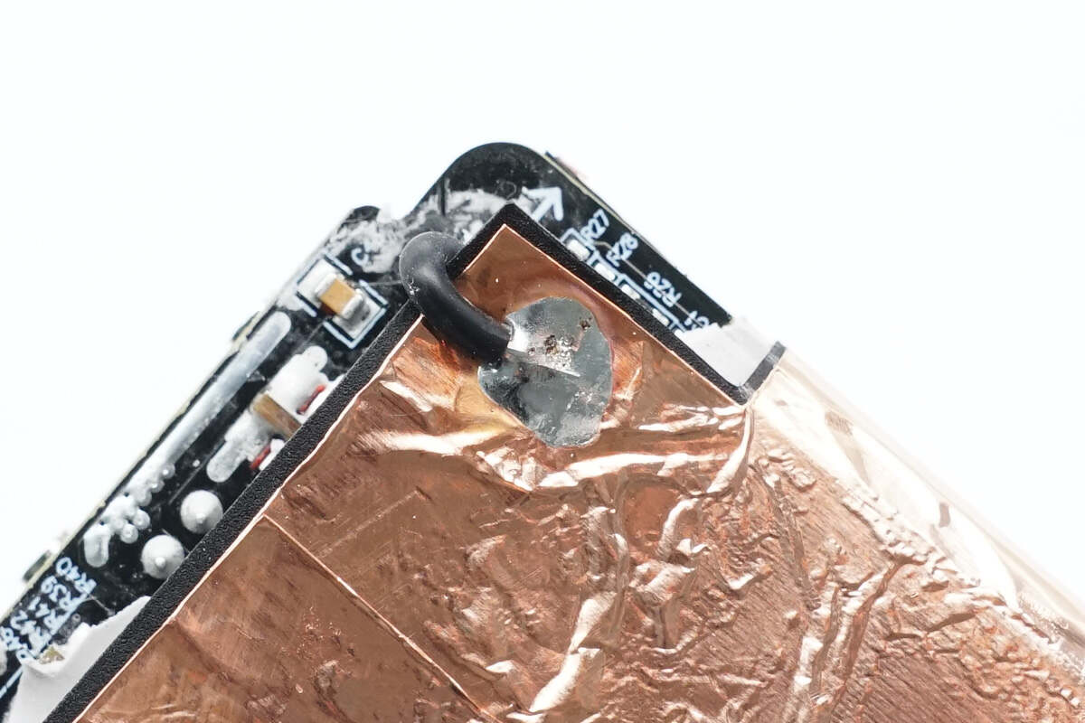
There is a cable connected to the PCBA module.
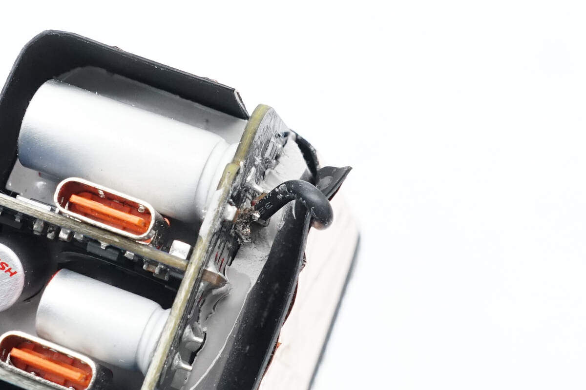
The other side of this cable is also connected to the PCBA module.
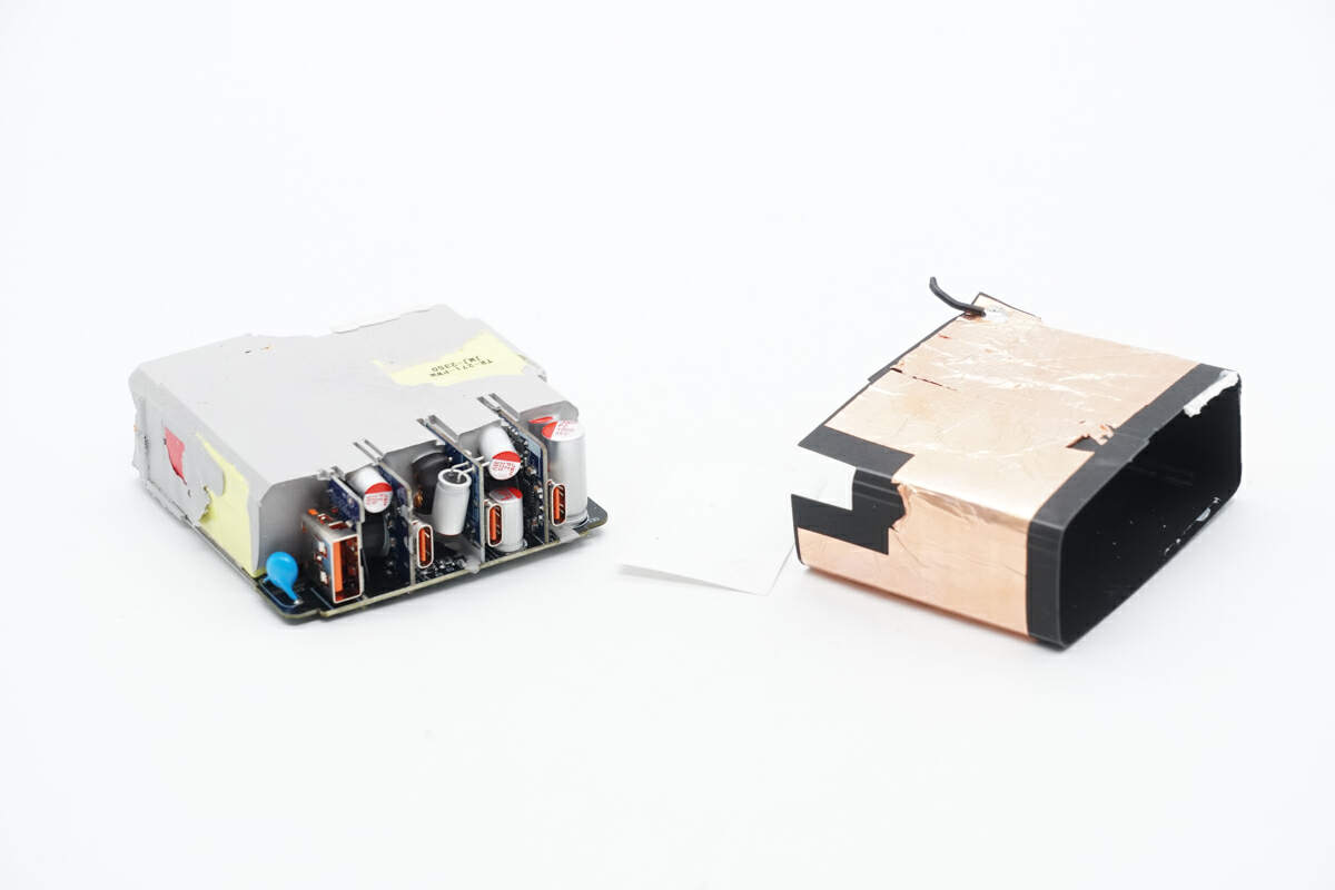
Remove the copper sheet and the mylar sheets.
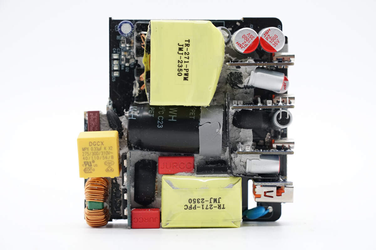
Clean up the PCBA module.
There are fuse, common mode choke, capacitors, and transformer on the front.
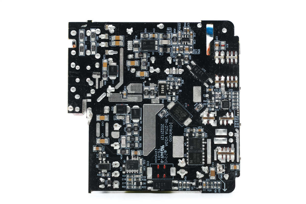
The PFC controller, PFC rectifier, flyback controller, optocouplers, SMD Y capacitor, and synchronous rectifiers are on the back.
ChargerLAB found it adopts PFC circuit and flyback topology. And it adopts three independent buck circuits to achieve four-port fast charging and automatic power distribution.
Next, we will take a look at each component starting from the input end.
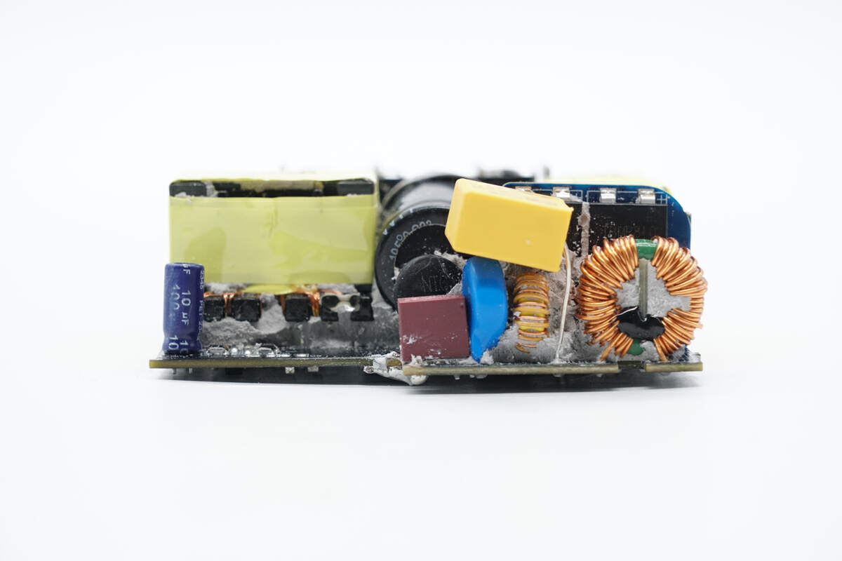
There are fuse, NTC thermistor, blue varistor, common mode choke, and safety X2 capacitor on the input end.
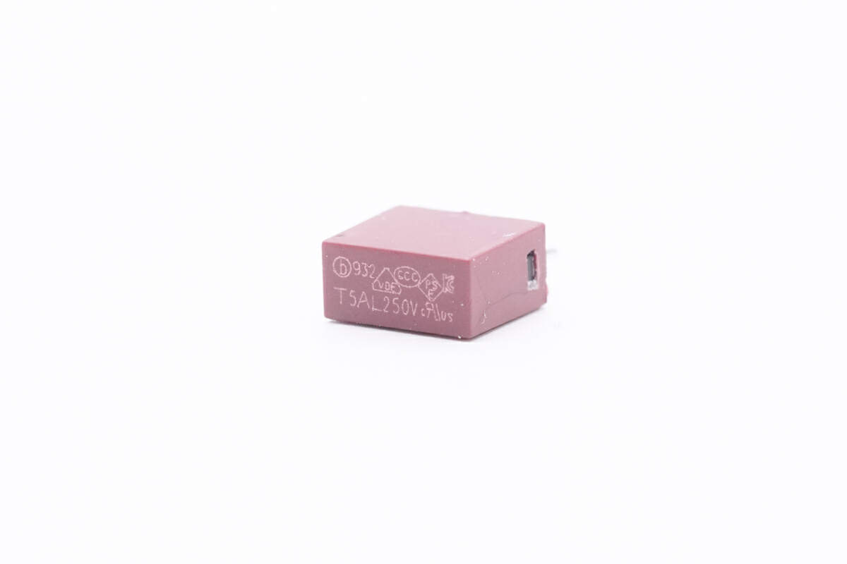
The input fuse marked with 932 is from Betterfuse. 5A 250V.
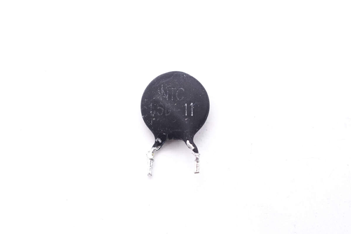
The varistor marked with 1.5D-11 is used to suppress the surge current.
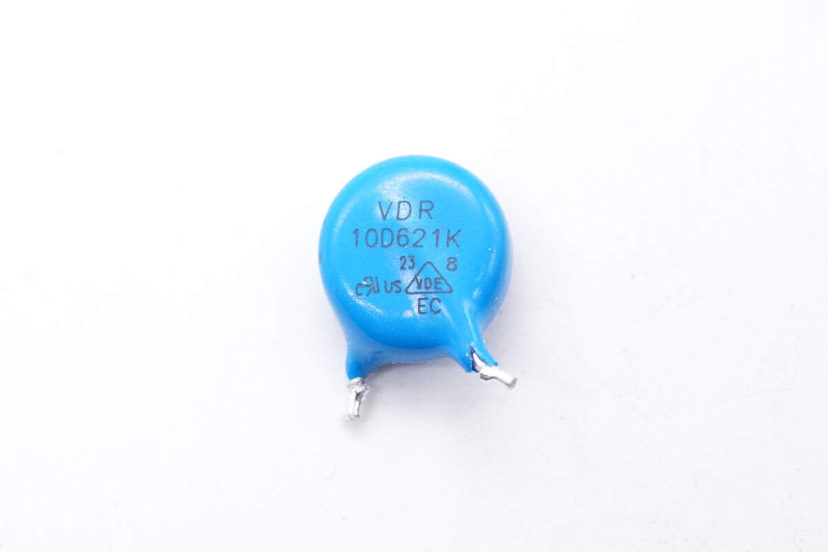
The blue varistor from SGLG is used for overvoltage protection. Model is 10D621K.
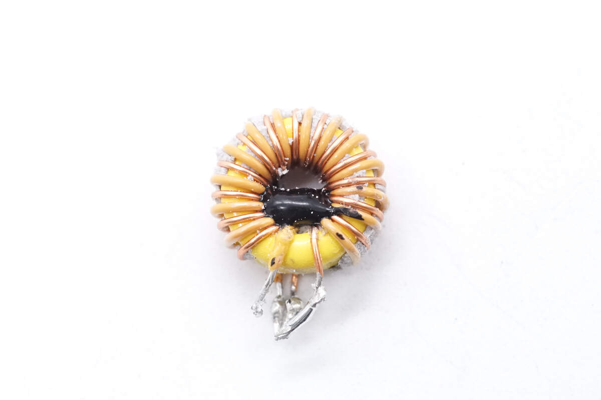
The common mode choke is wound with magnet and insulated wires.
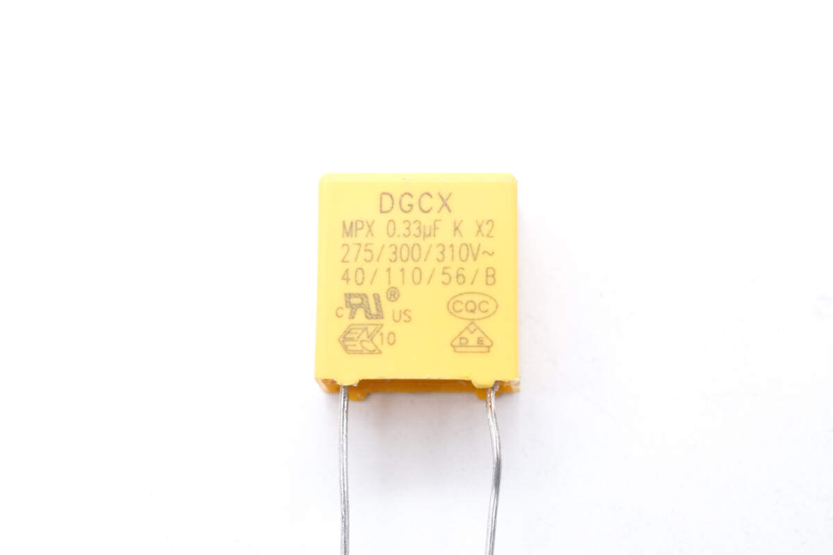
The safety X2 capacitor is from DGCX. 0.33μF.
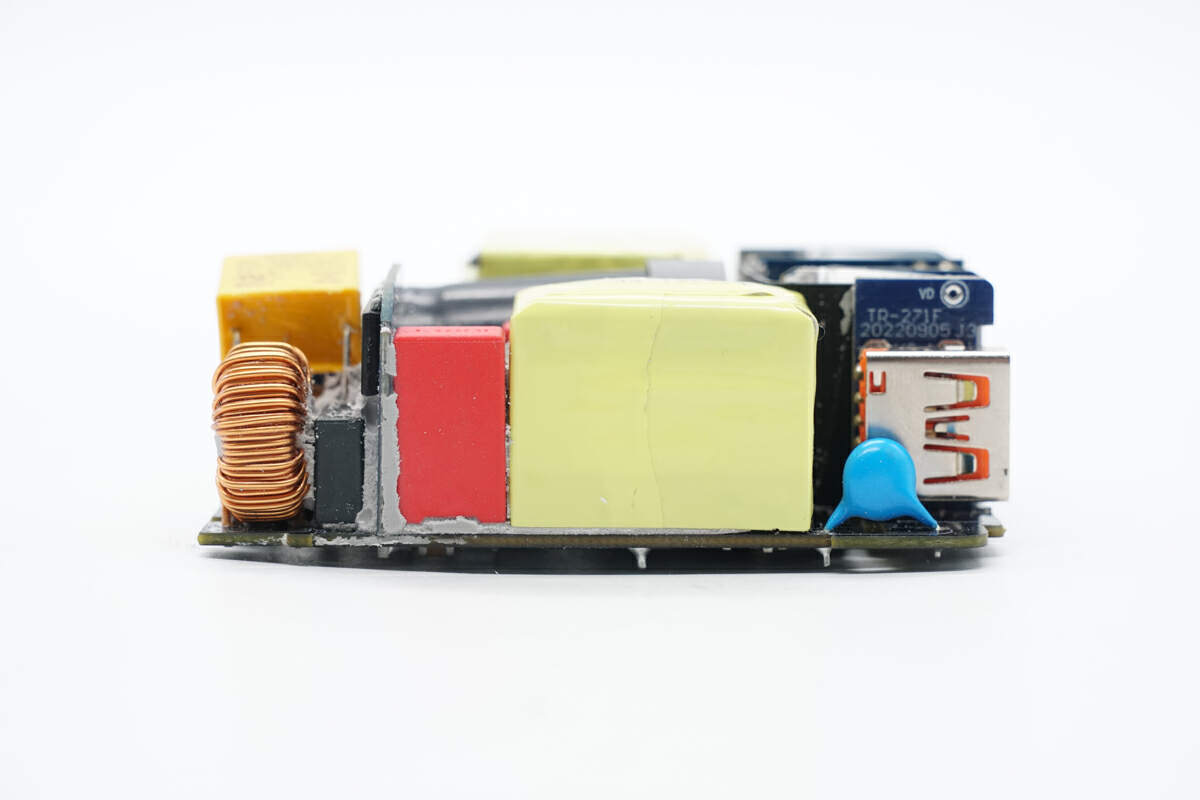
There are common mode choke, safety X2 capacitor, film filter capacitors, and PFC boost inductors on the side of the PCBA module.
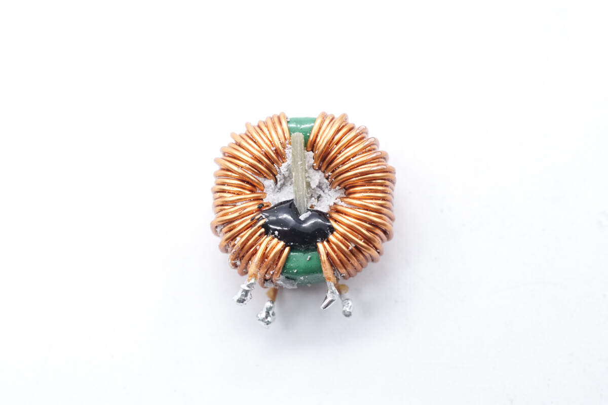
The common mode choke is wound with magnet and insulated wires.
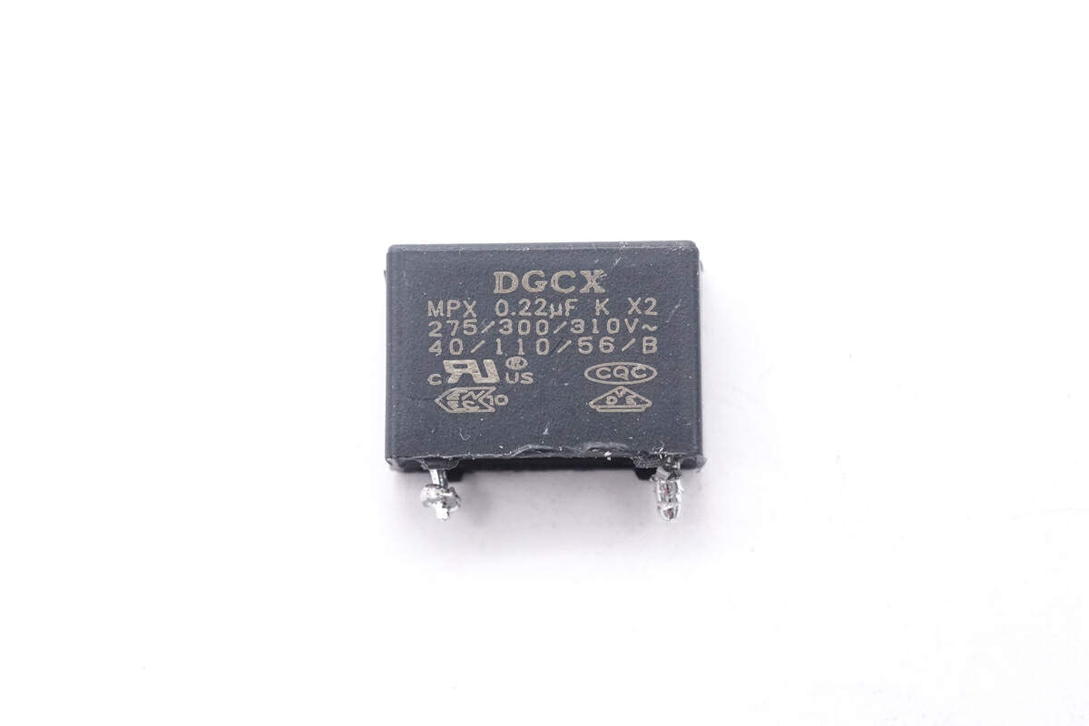
The other safety X2 capacitor is also from DGCX. 0.22μF.
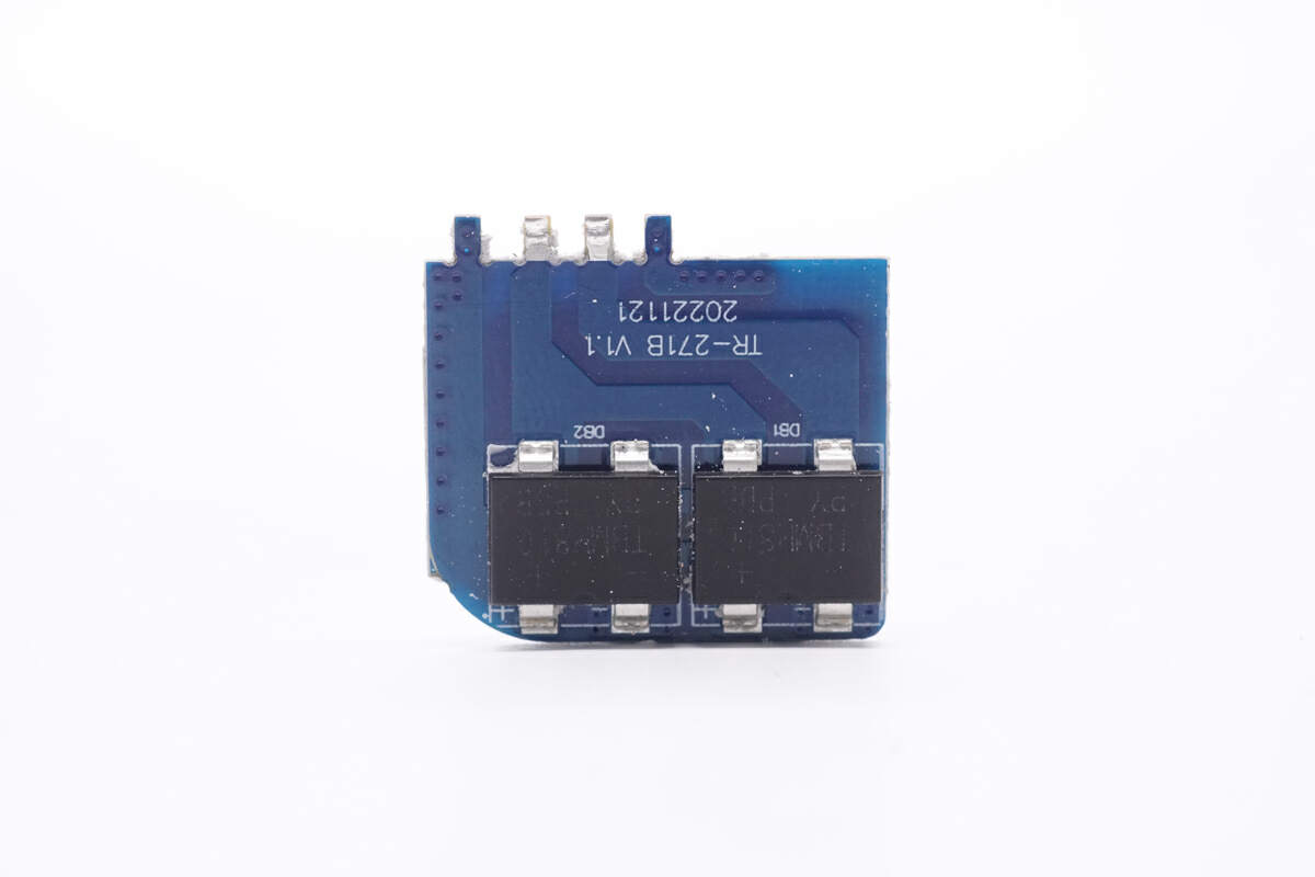
The bridge rectifier is soldered on a small PCB.
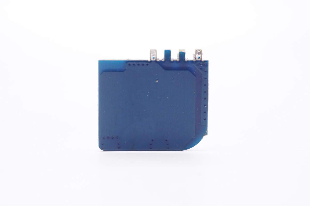
There are no components on the back of this small PCB.
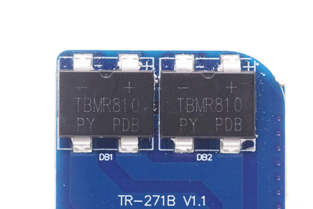
The bridge rectifiers are from Pingwei. They are connected in parallel to reduce temperature rise. Model is TBMR810. 8A 1000V.
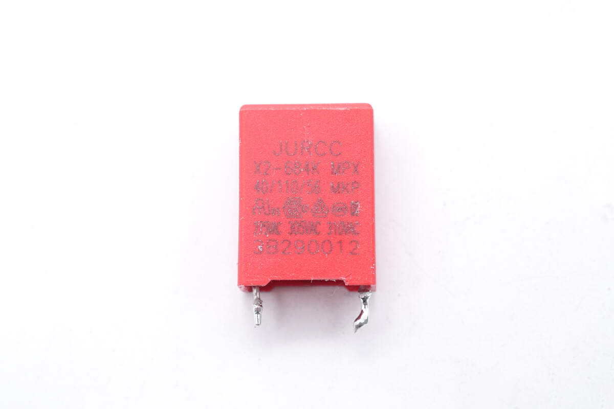
The film capacitor is from JURCC. 0.68μF.
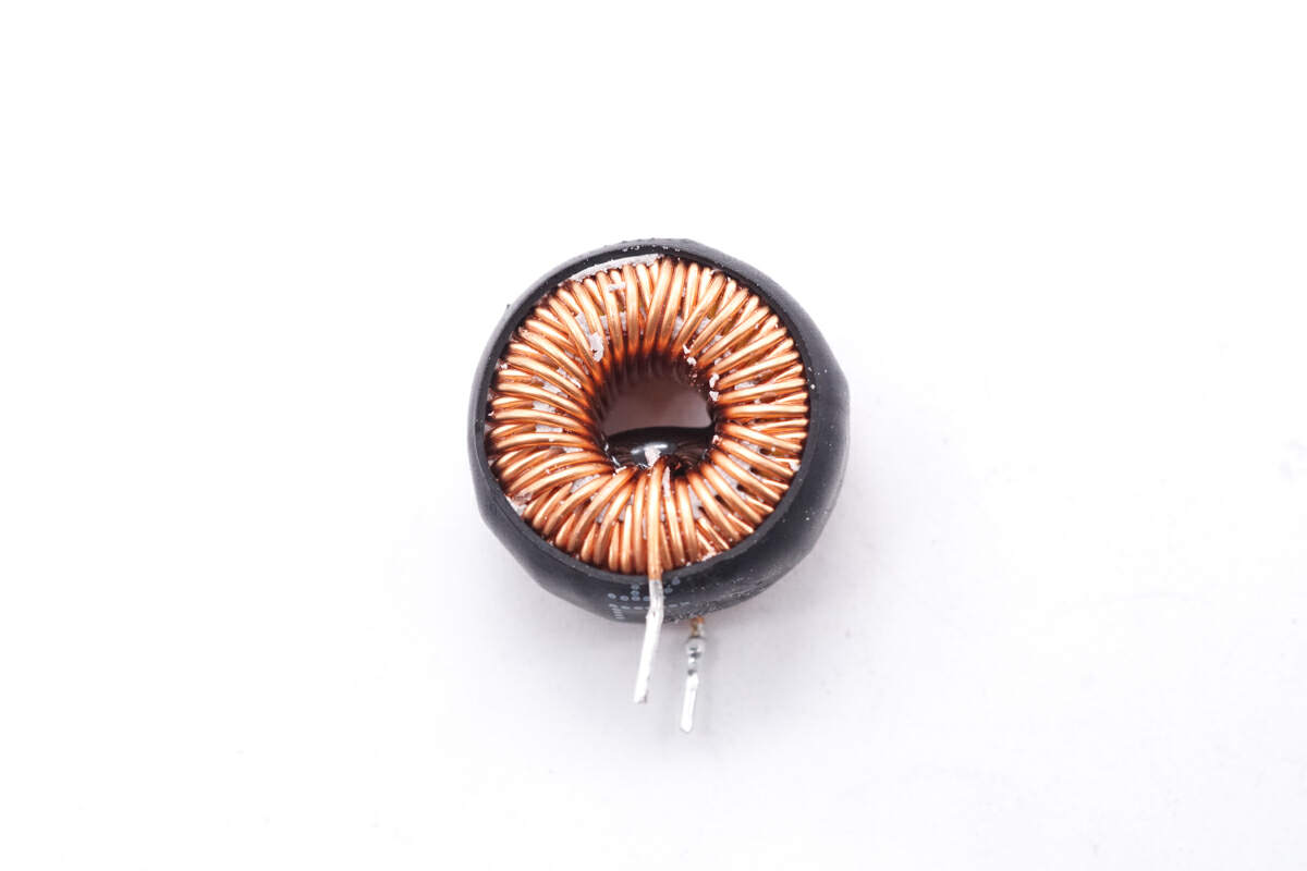
The filter inductor is wounded with magnetic ring and insulated by heat-shrinkable tubing.
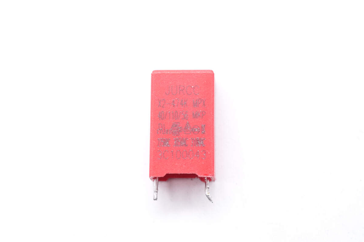
Here is another filter inductor. 0.47μF.
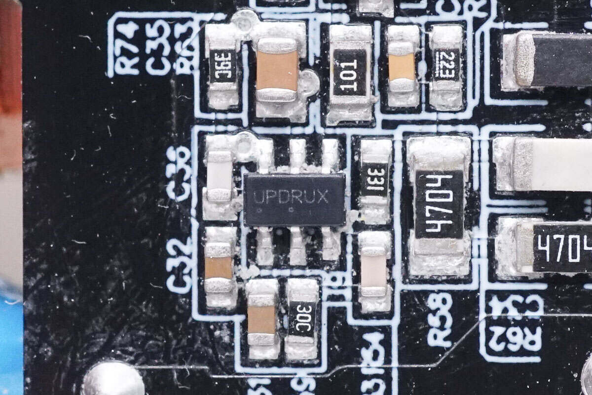
The PFC controller is from Onsemi. It is based on an innovative Valley Synchronized Frequency Fold-back (VSFF) method, it operates in critical conduction mode (CrM) until the power drops below a threshold level. The VSFF maximizes the efficiency at both nominal and light loads. Model is NCP1623.
It will enter discontinuous conduction mode (DCM) with increased dead-time as the load further decays (frequency foldback).

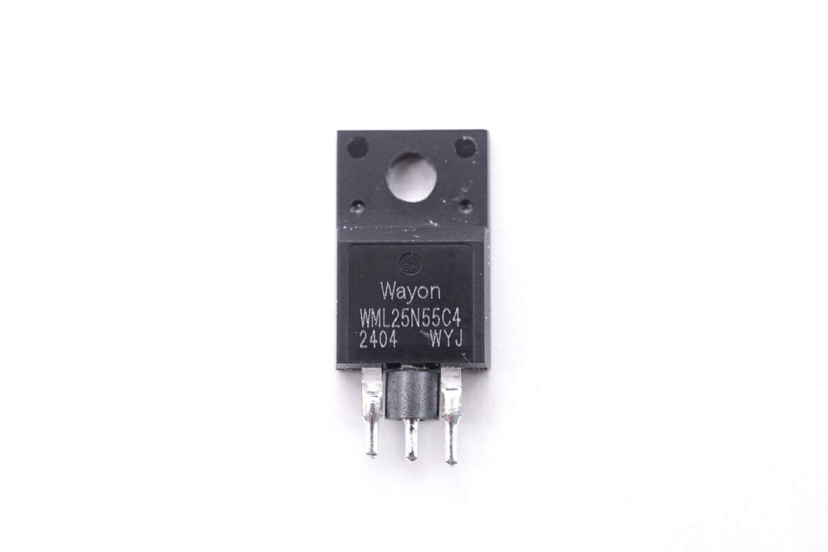
The PFC MOSFET is from WAYON and adopts TO220F package. Model is WML25N55C4. 550V.
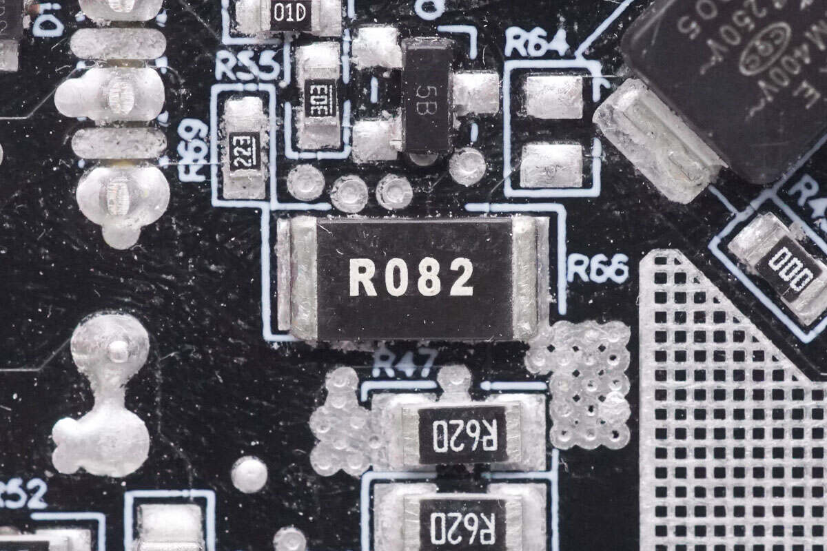
The sampling resistor is used to detect the current of the MOSFET. 82mΩ.
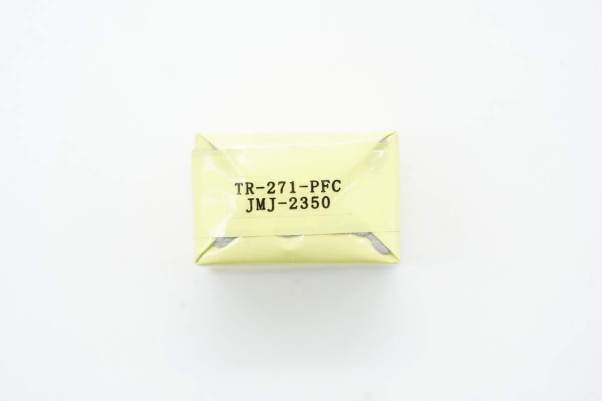
The PFC boost inductor is insulated by tape.
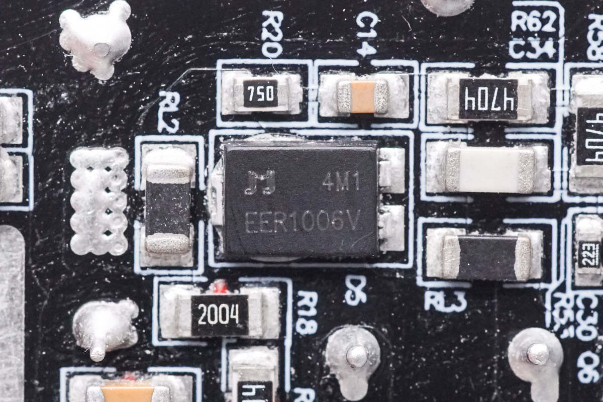
The PFC rectifier is from JJM and adopts TO-277B package. Model is JEER1006V. 600V 10A.
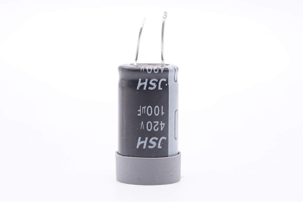
The electrolytic capacitor for input filtering is from JSH. The top of the capacitor is insulated with a silicone cap. 420V 100μF.
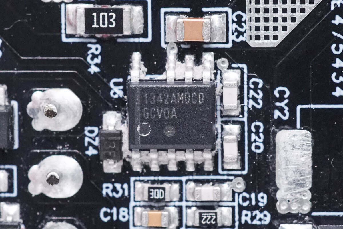
The master control chip is from Onsemi. It is a high-frequency resonant PWM controller with flyback topology. It supports a wide range of power supply, overheating protection, and other protection functions. Model is NCP1342.
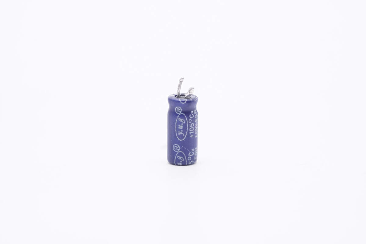
The filter capacitor that powers the master control chip is from Yuguang.
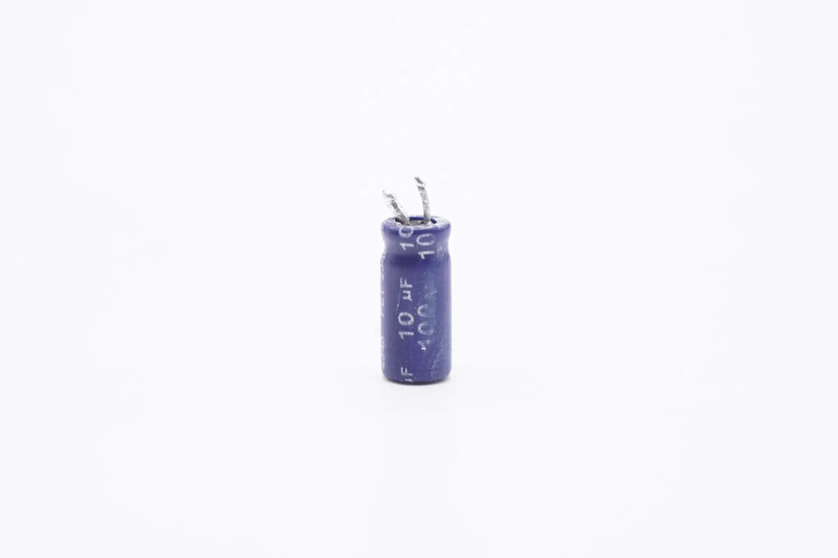
Its specification is 10μF 100V.
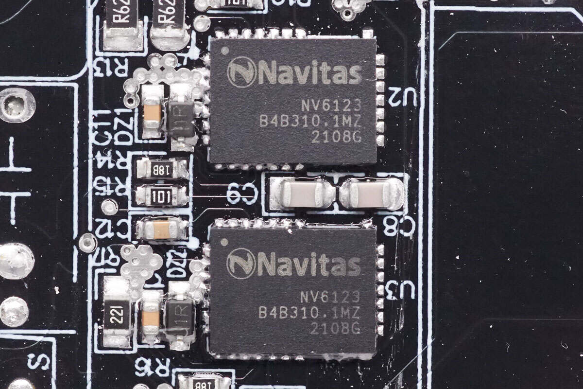
These two MOSFETs are from Navitas and they are connected in parallel. Model is NV6123. 300mΩ.
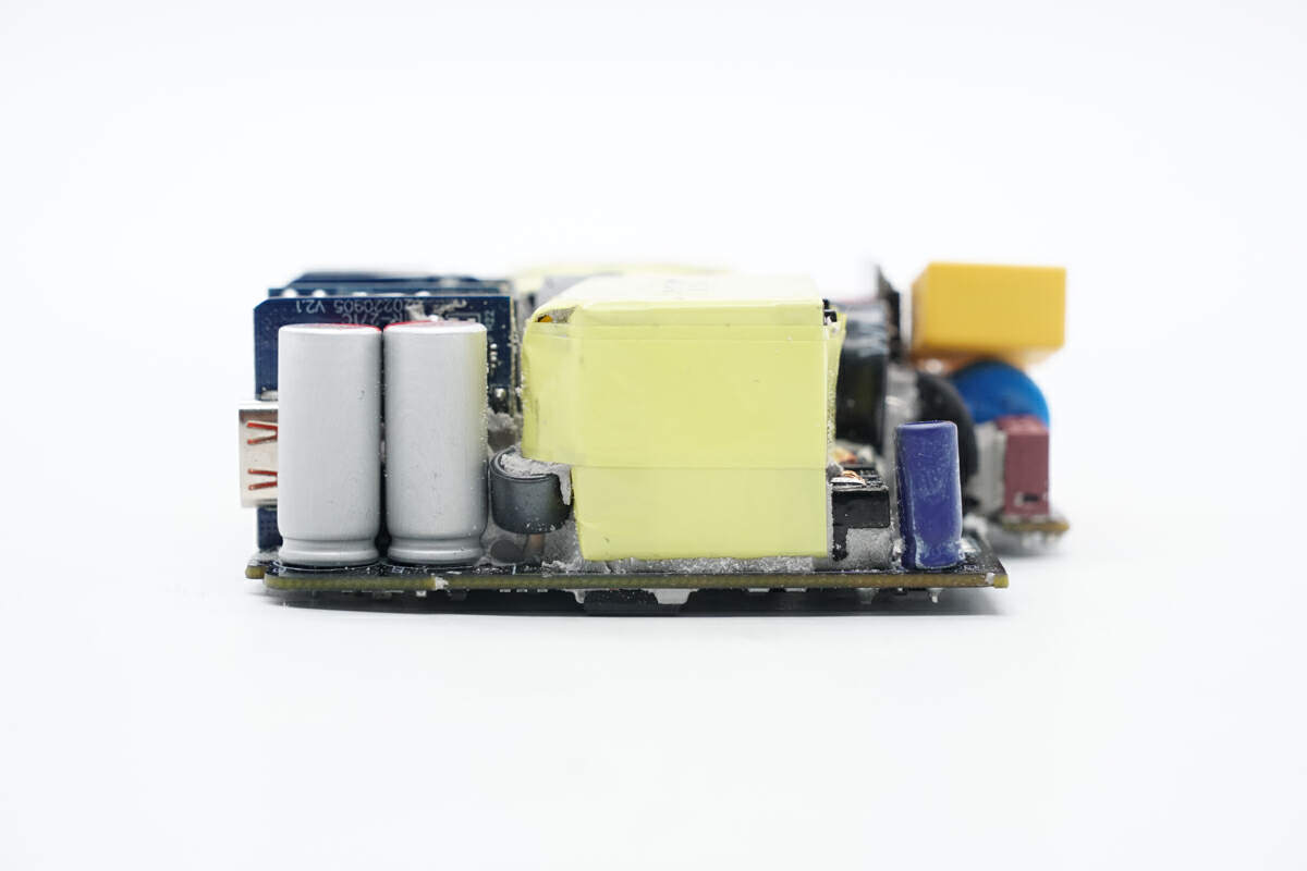
Here are the filter capacitors and the transformer.
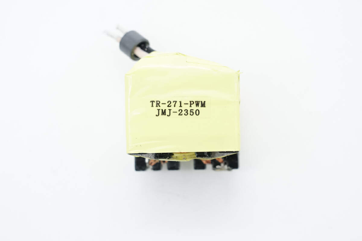
The transformer is insulated by tape.
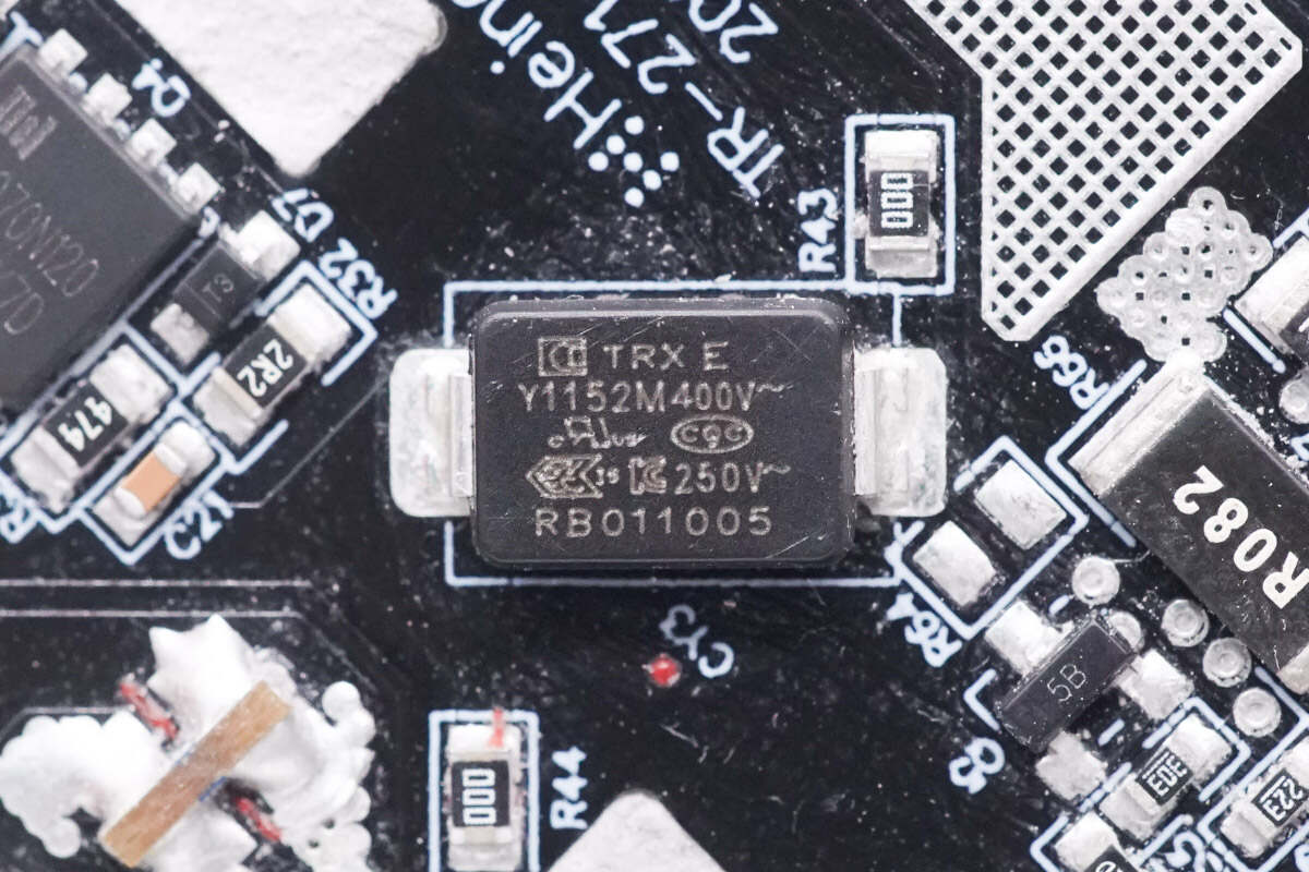
The SMD Y capacitor is from TRX. Its small size and light weight are suitable for high-density power products such as GaN fast chargers. Model is TMY1152M.
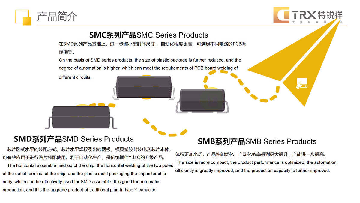
Here are some information about TRX products.
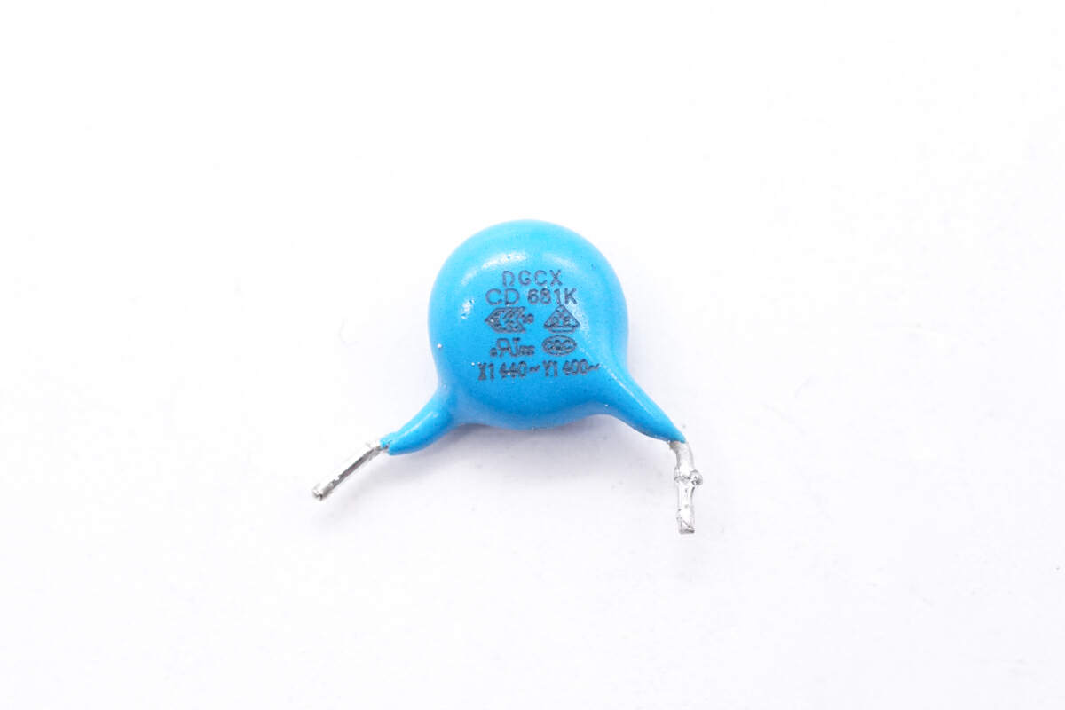
This blue Y capacitor is from DGCX.
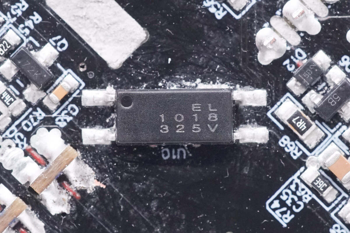
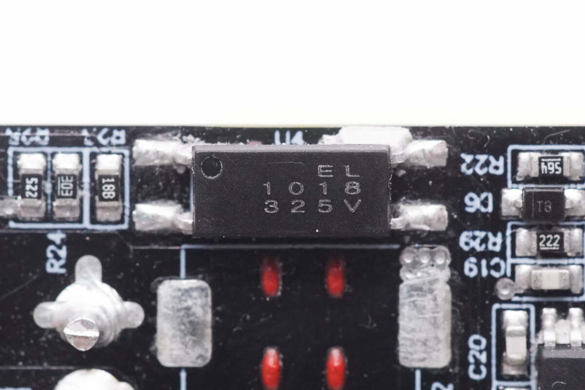
The optocoupler from Everlight is used for PFC control. Model is EL1018.
Another optocoupler is used for output voltage feedback.
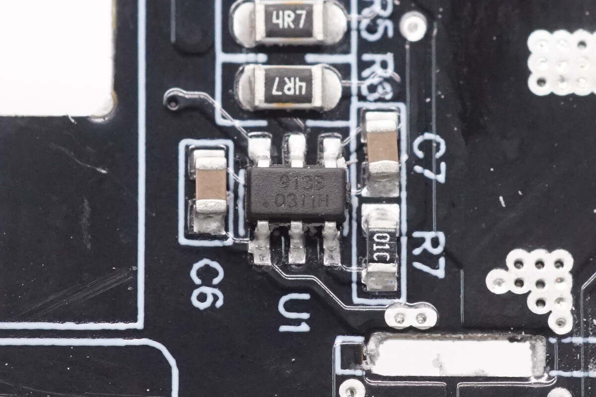
The digital multi-mode synchronous rectifier controller is from HYASiC and it can support multiple working modes such as DCM, CCM, PFM, and QR. It can also support power supply voltage range of 3-25V. Model is HY913B.
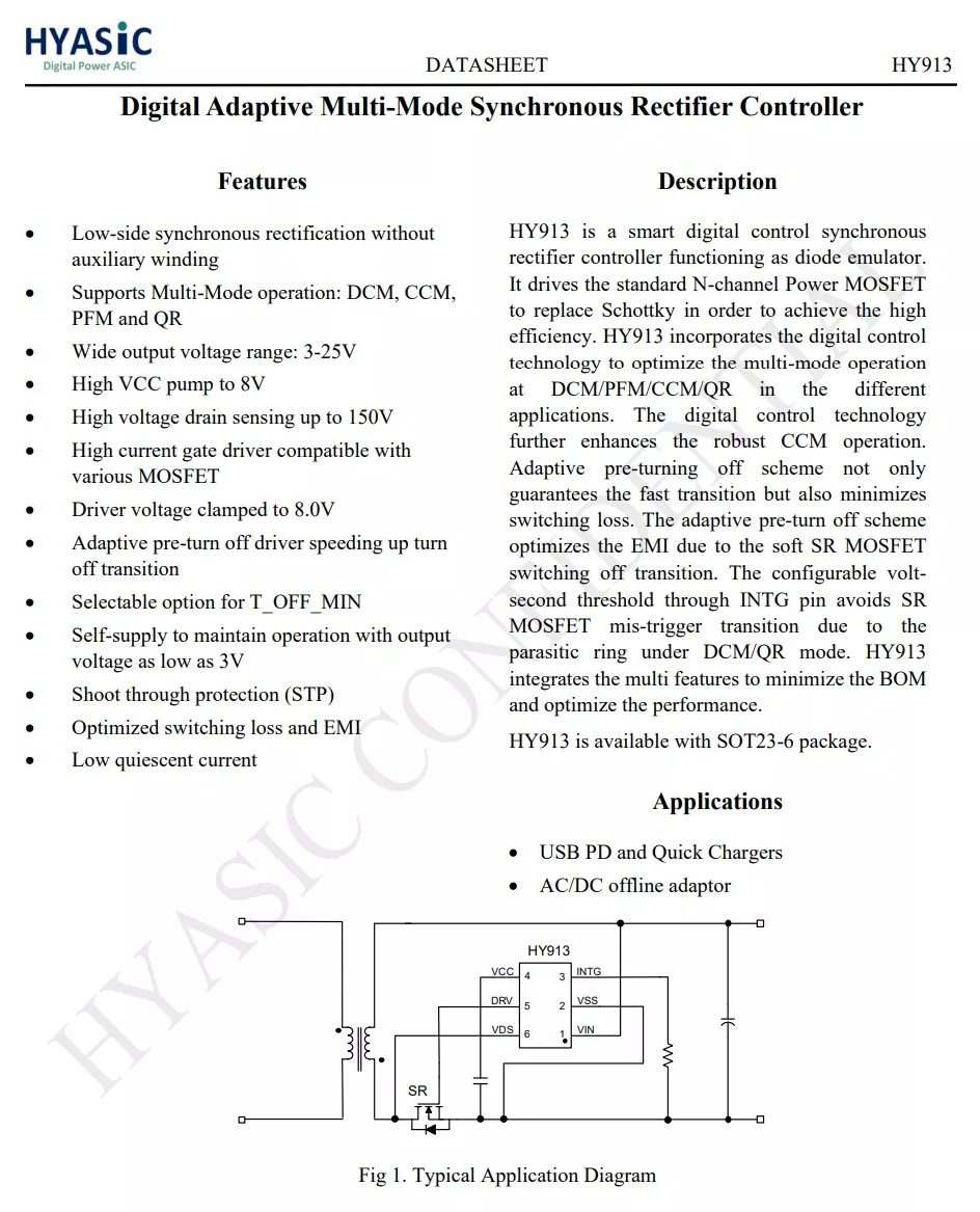
Here is all the information about HYASiC HY913.
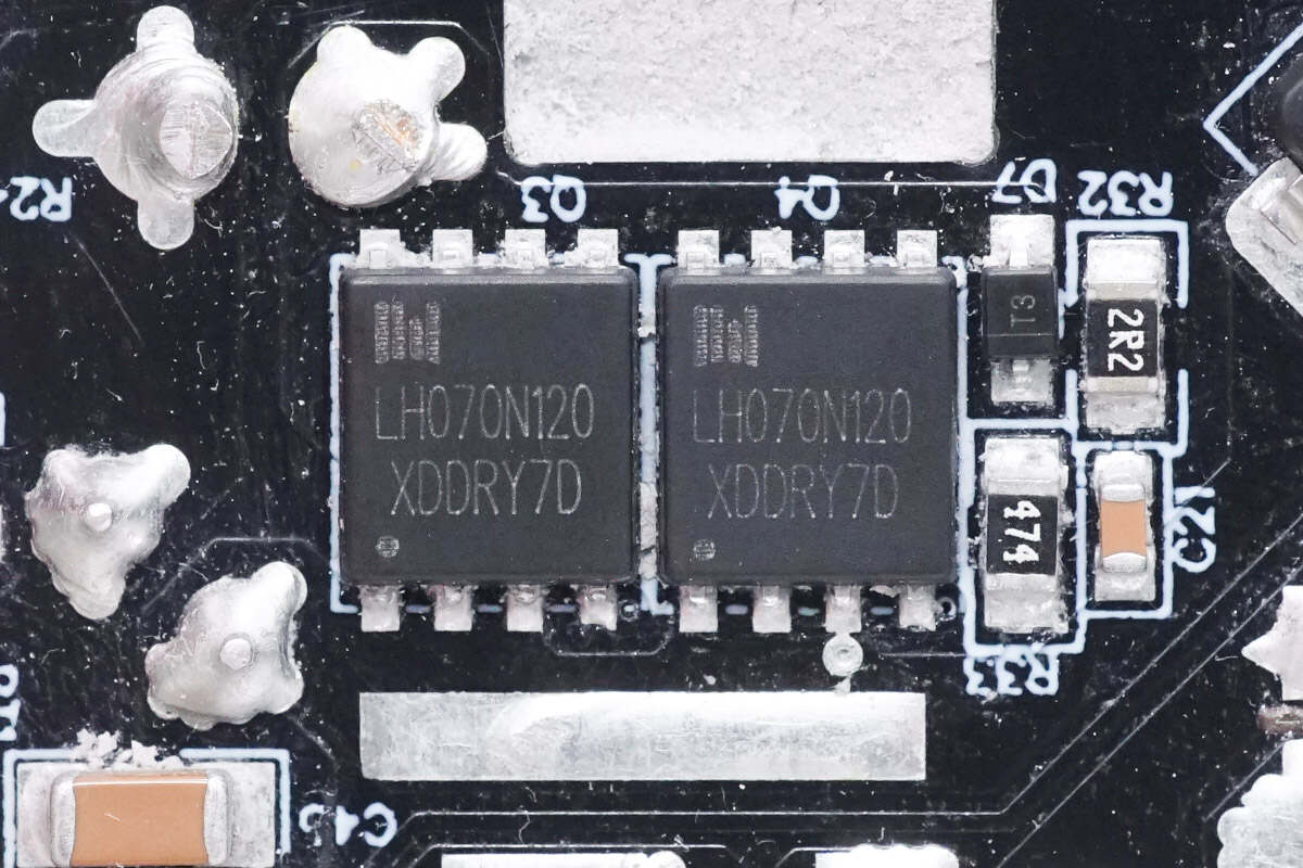
These two synchronous rectifiers are from LIHOMICRO and adopt DFN5 x 6 package. Model is LH070N120. 120V 7mΩ.
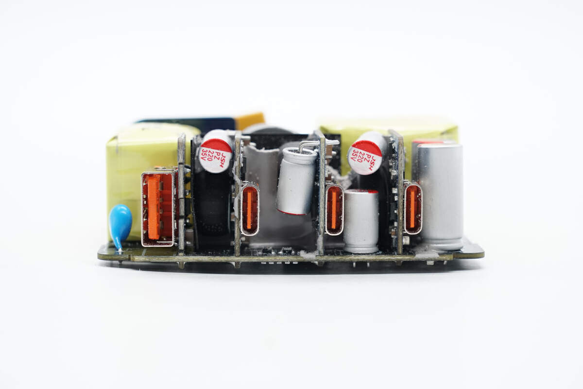
The output side has three USB-C socket PCBs. And there are filter capacitors and buck inductors on the PCBs.
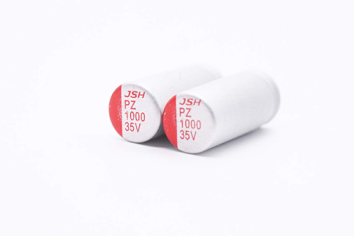
These two solid capacitors for output filtering are from JSH. 1000μF 35V.
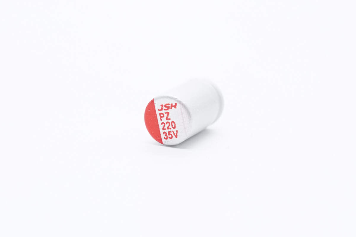
This is another solid capacitor for output filtering. 220μF 35V.
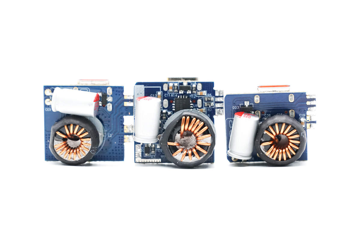
There are filter capacitors and buck inductors on the front of the USB-C buck PCBs.
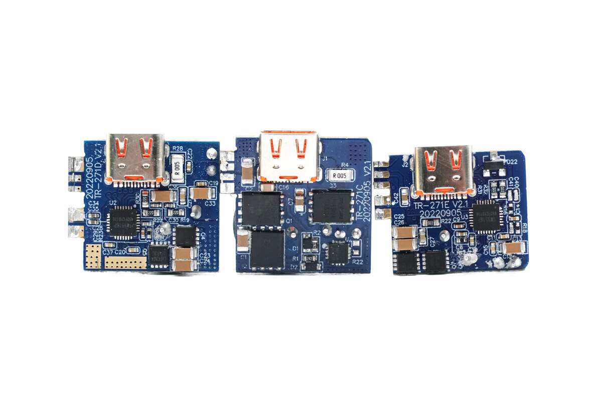
The USB-C sockets, buck protocol chips, and MOSFETs are soldered on the back of the PCBs.
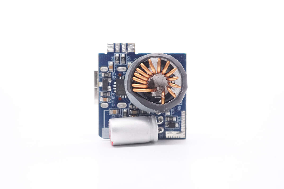
There are protocol chip, buck inductor, and filter capacitor for output filtering on the PCB of USB-C1.
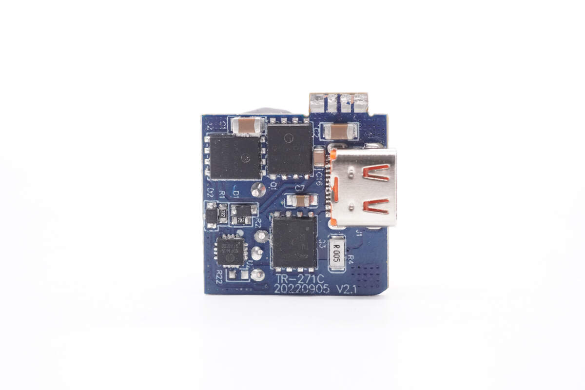
The back of the USB-C1 PCB has the synchronous buck controller, synchronous buck MOSFET, VBUS MOSFET, and USB-C socket.
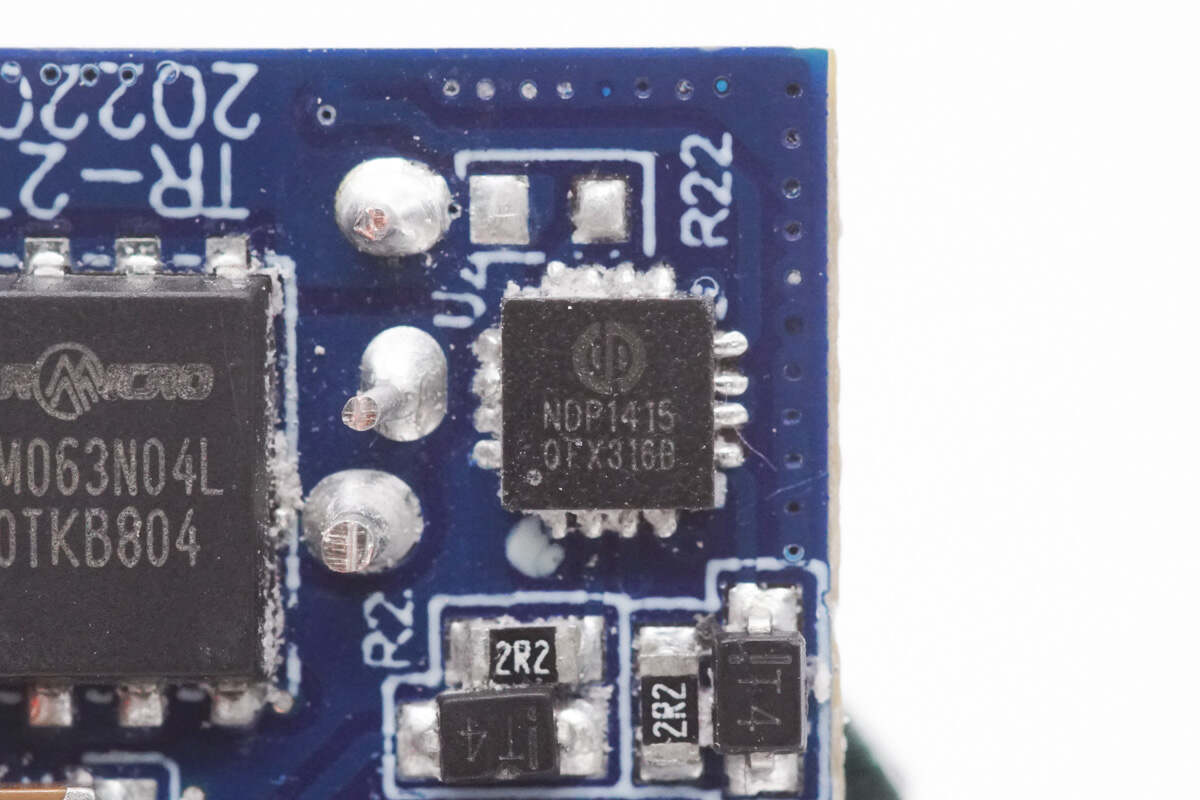
The synchronous buck controller is from Deep-pool. It can support an input voltage of 38V and loss compensation. Model is NDP1415.
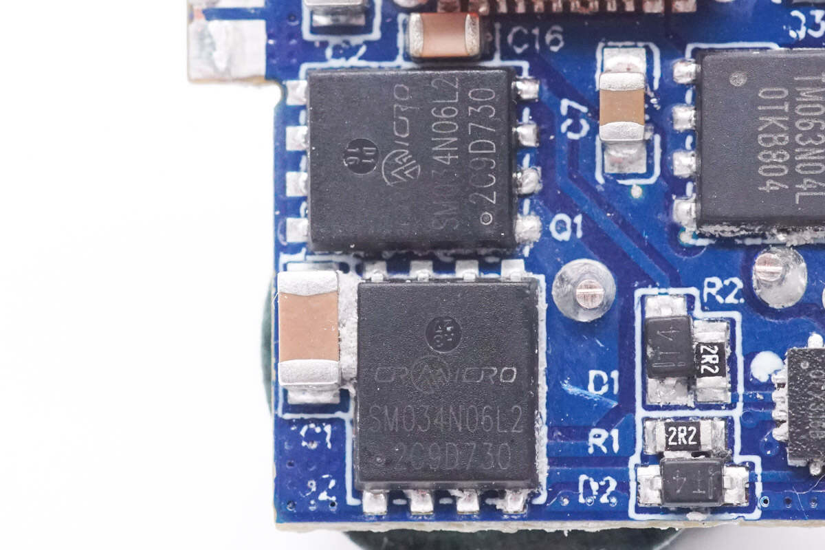
These two synchronous buck MOSFETs are from CR MICRO and adopt DFN5 x 6 package. Model is CRSM034N06L2. 60V 2.8mΩ for each.
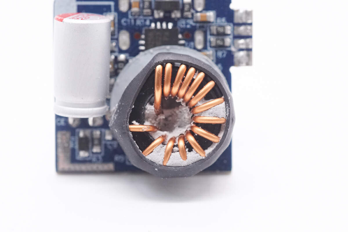
The buck inductor is insulated by heat-shrinkable tubing.
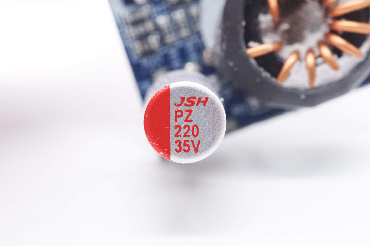
The solid capacitor for output filtering is from JSH. 220μF 35V.
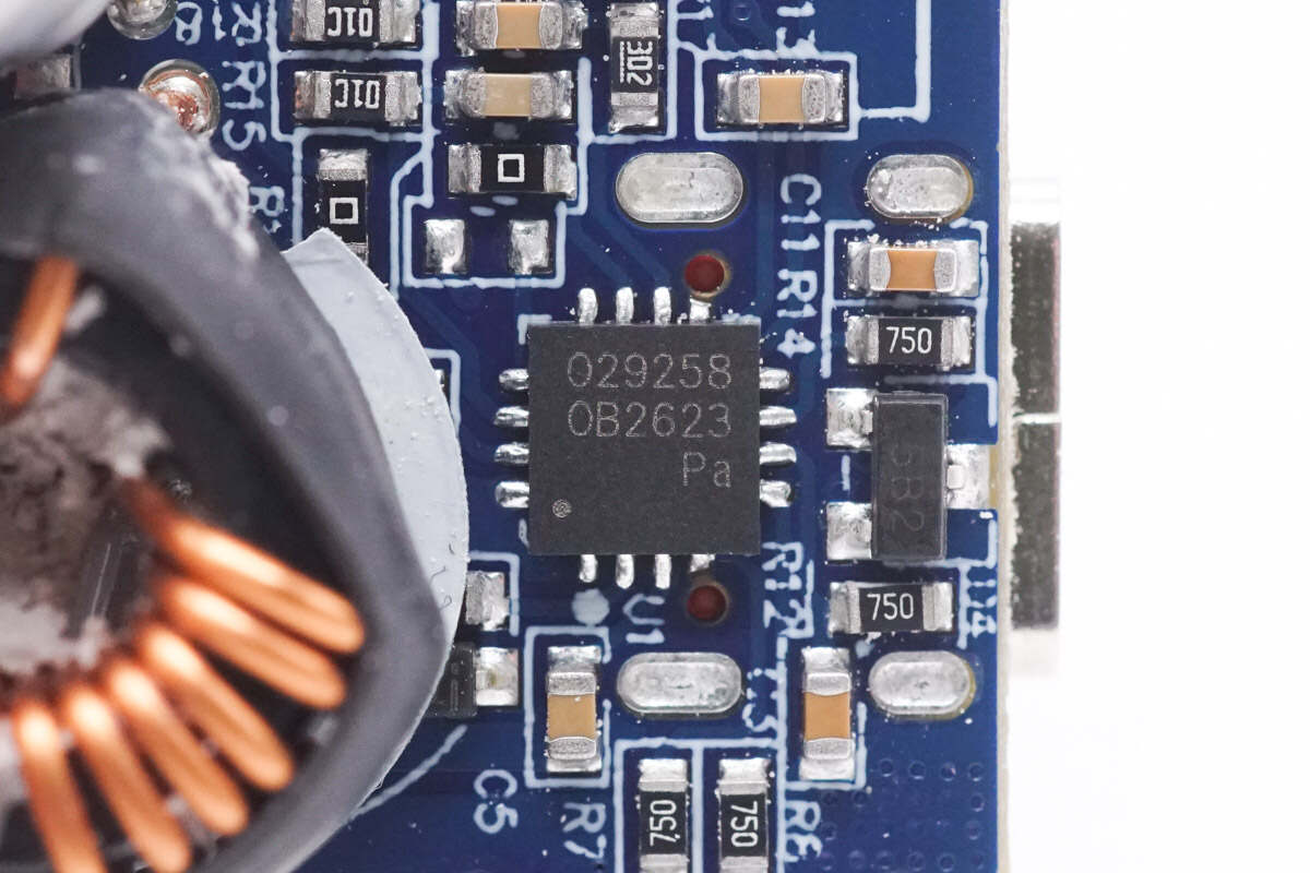
The protocol chip is from On-Bright and adopts QFN16 package. It can support PD3.1, output of 28V, and an output of 140W. It also supports CC/CV modes. Model is OB2623.
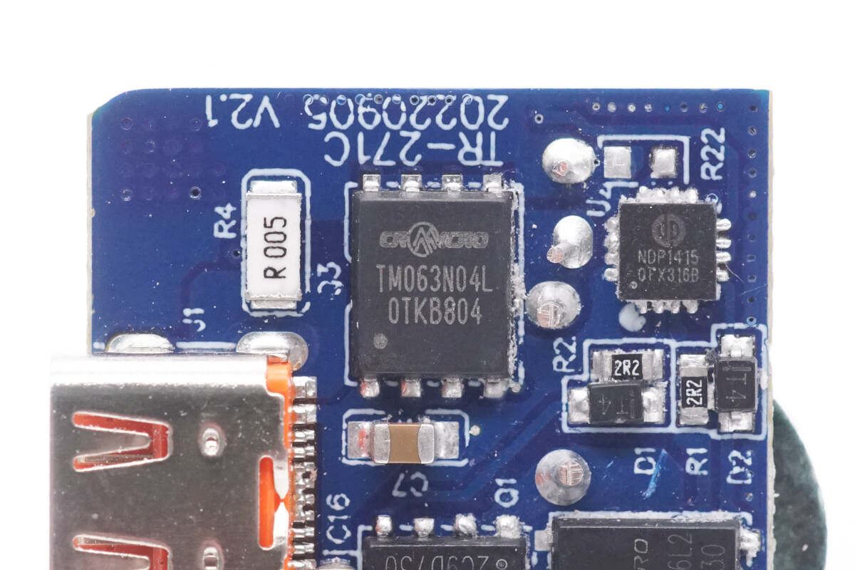
The VBUS MOSFET is from CR MICRO and adopts DFN5 x 6 package. Model is CRTM063N04L. 40V 4.5mΩ.
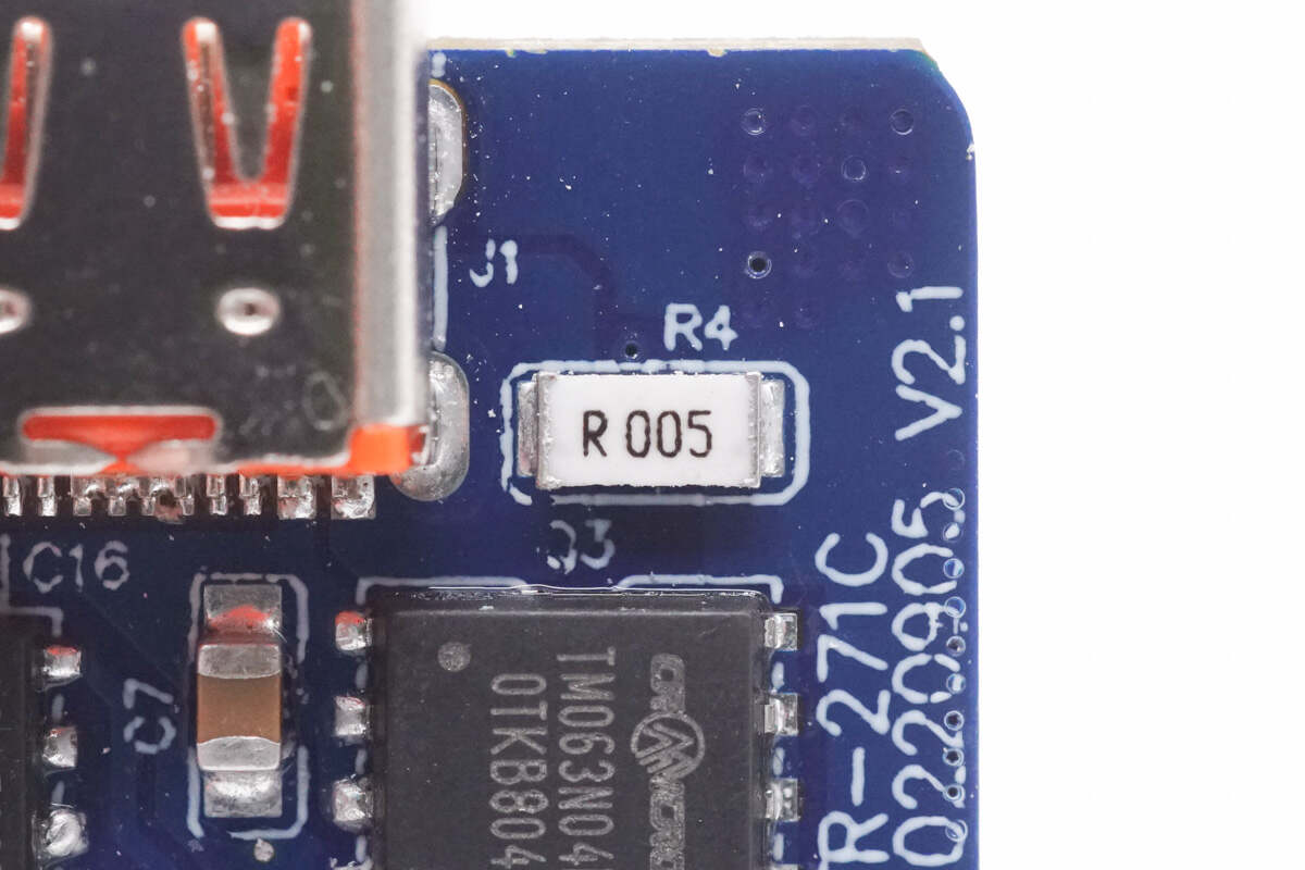
The resistor is used to detect the output current. 5mΩ.
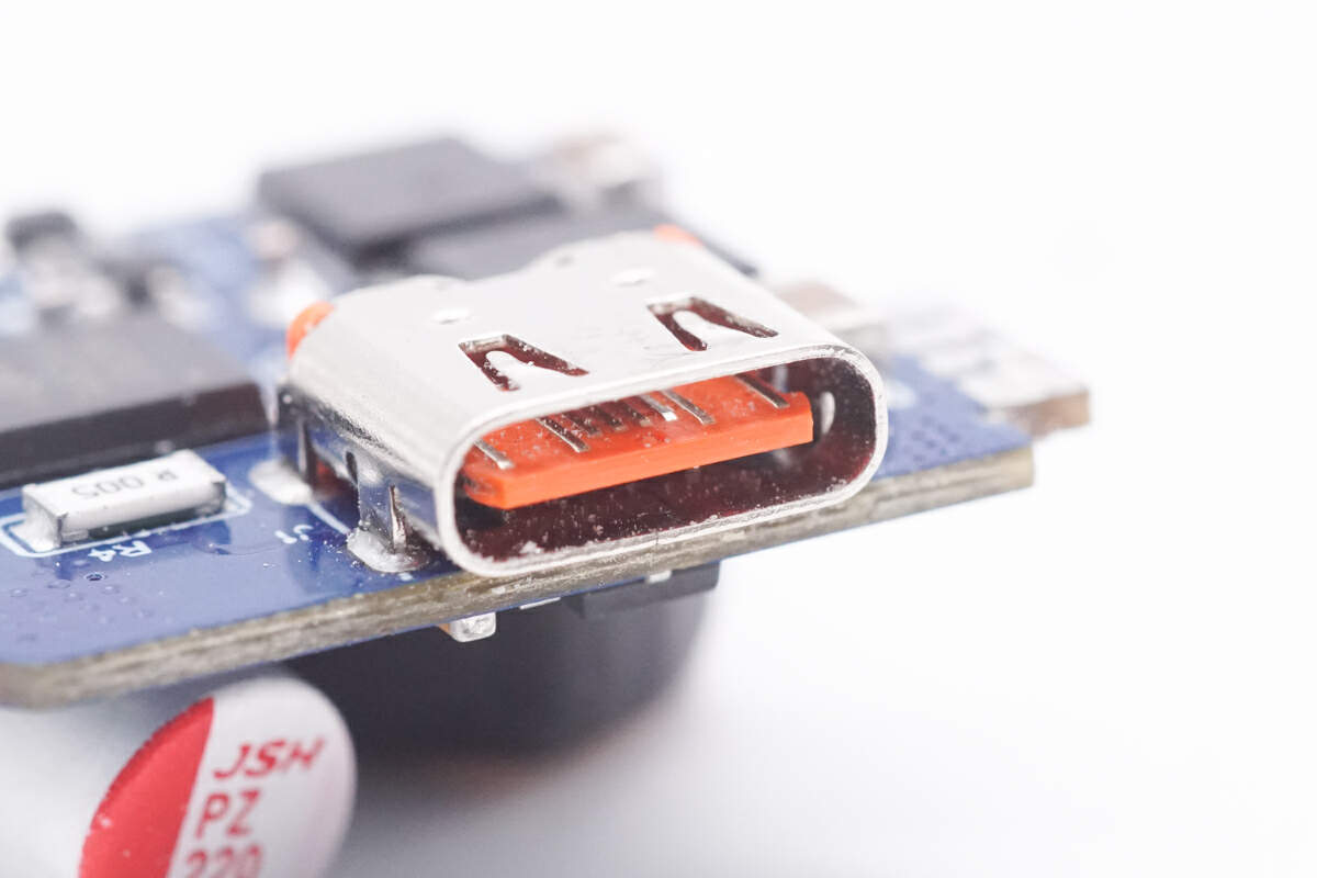
Here is the orange USB-C socket.
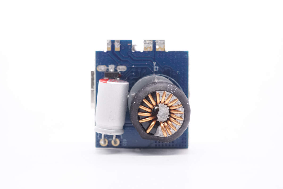
The buck inductor and filter capacitor are on the PCB of USB-C2.
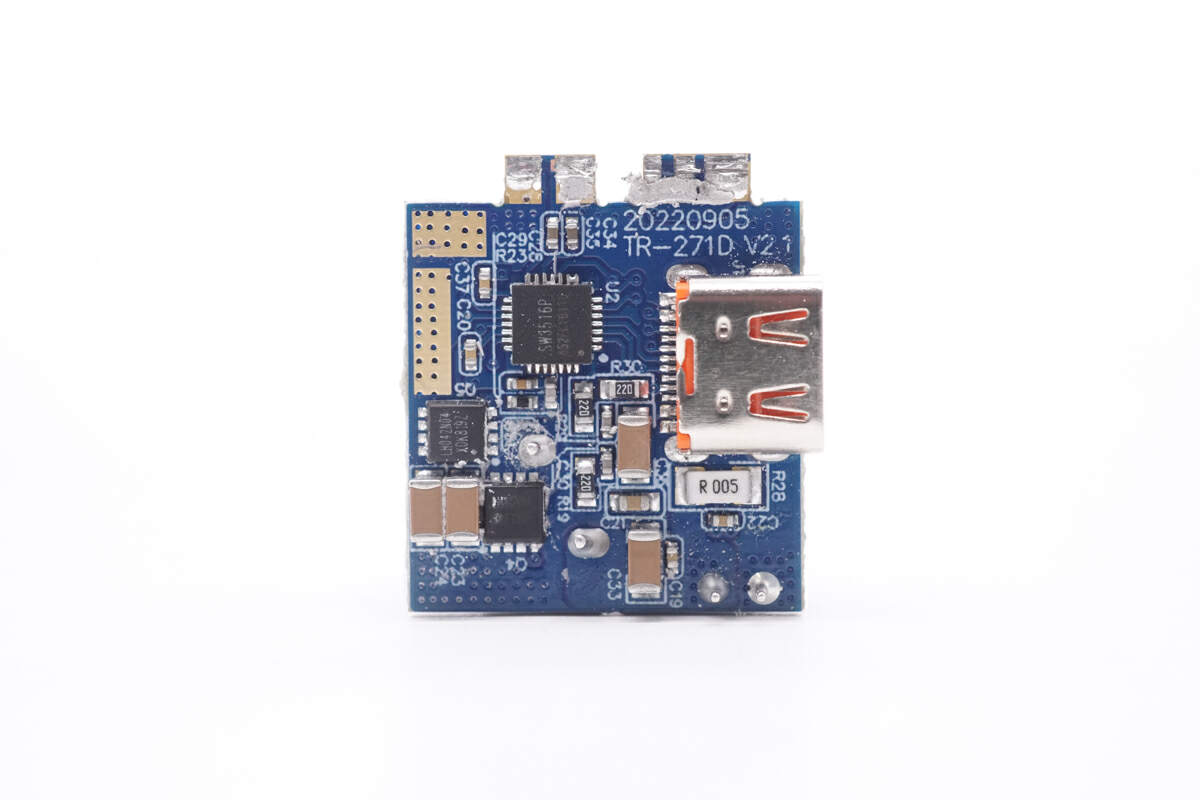
The other side contains the buck protocol chip, synchronous buck MOSFETs, and USB-C socket.
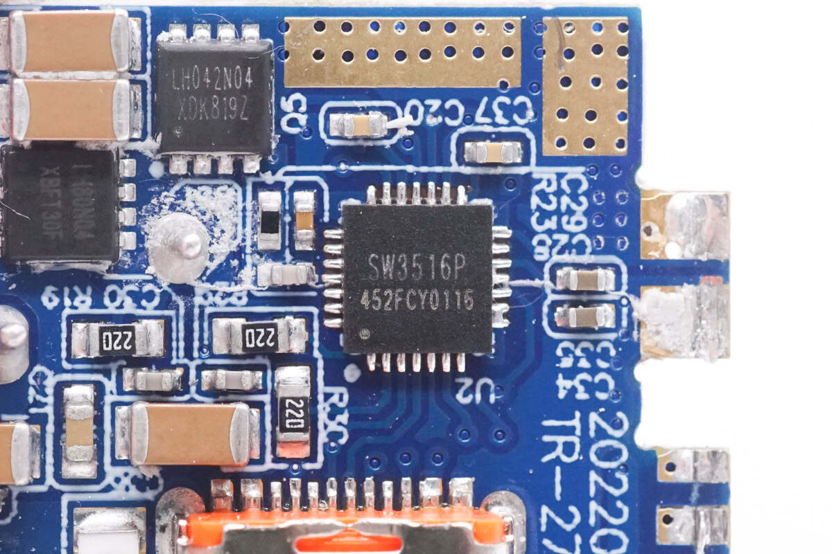
The buck protocol chip is from iSmartWare. It supports multiple protocols and dual-port independent current limiting. It can also be used in fast charging of any USB-C and USB-A ports. Model is SW3516P.
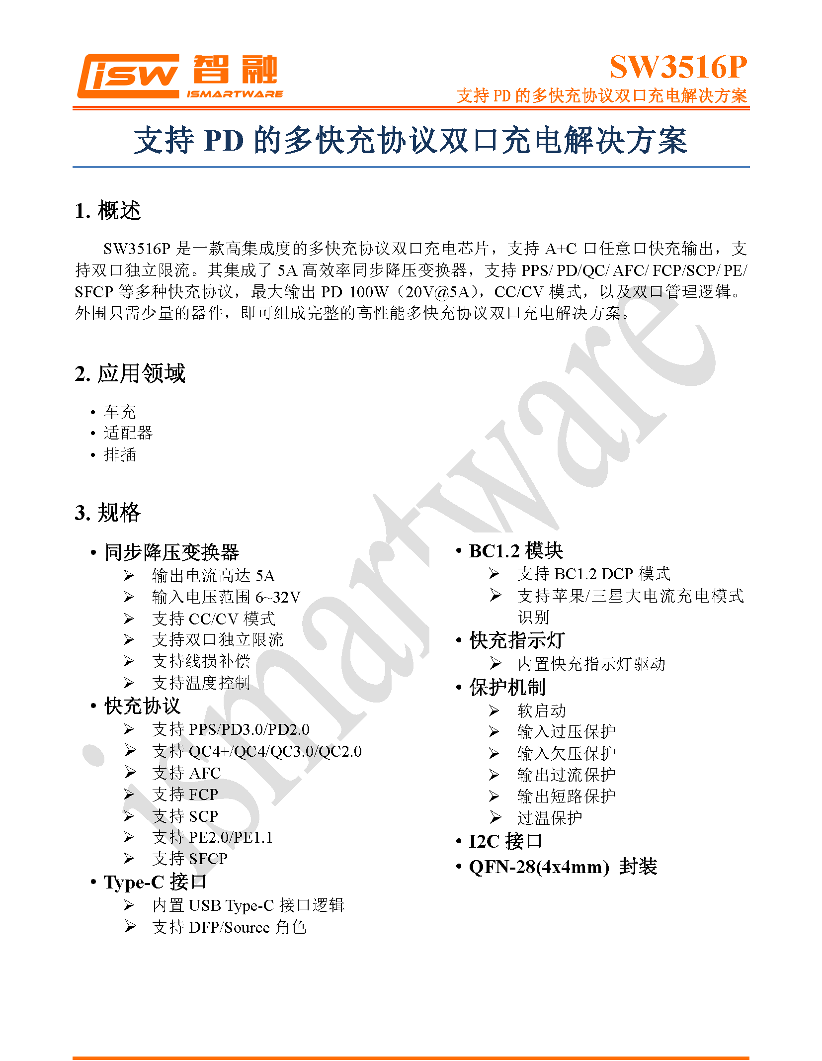
Here is all the information about the iSmartWare SW3516P.
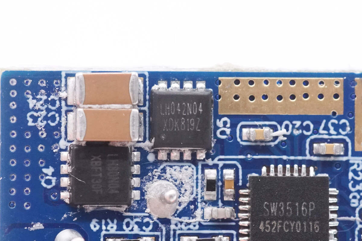
This synchronous buck MOSFET is from LIHOMICRO and adopts DFN3 x 3 package. Model is LH042N04. 40V 4.2mΩ.
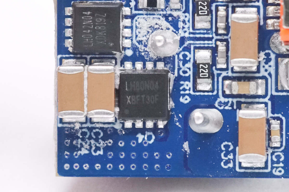
Another synchronous buck MOSFET is also from LIHOMICRO and adopts DFN3 x 3 package. Model is LH80N04. 40V 5.5mΩ.
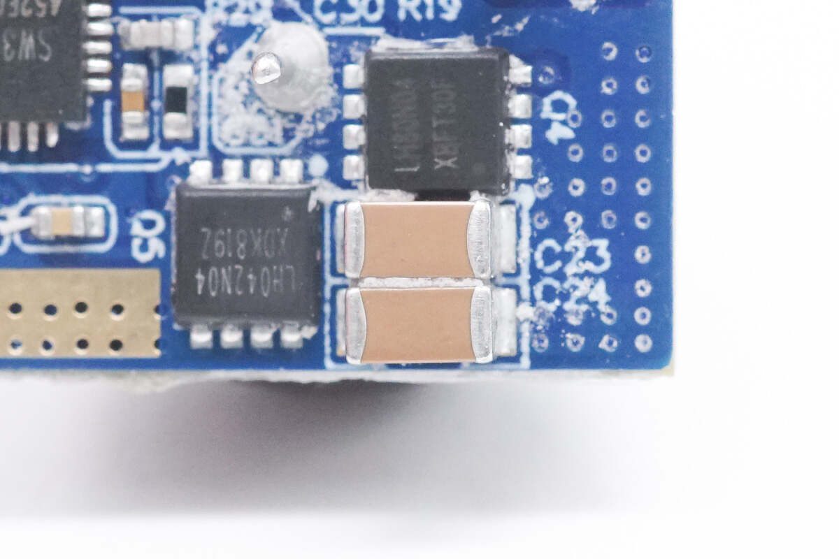
Here are two MLCC capacitors.
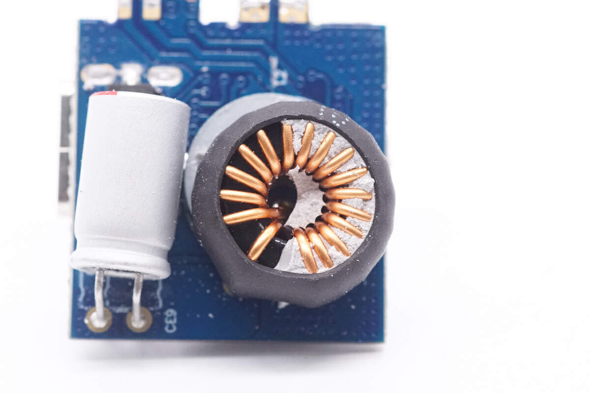
The buck inductor is insulated by heat-shrinkable tubing.
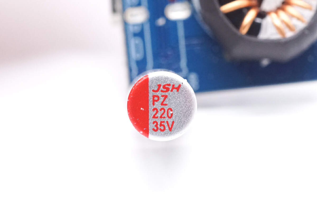
Here is the solid capacitor for output filtering. 220μF 35V.
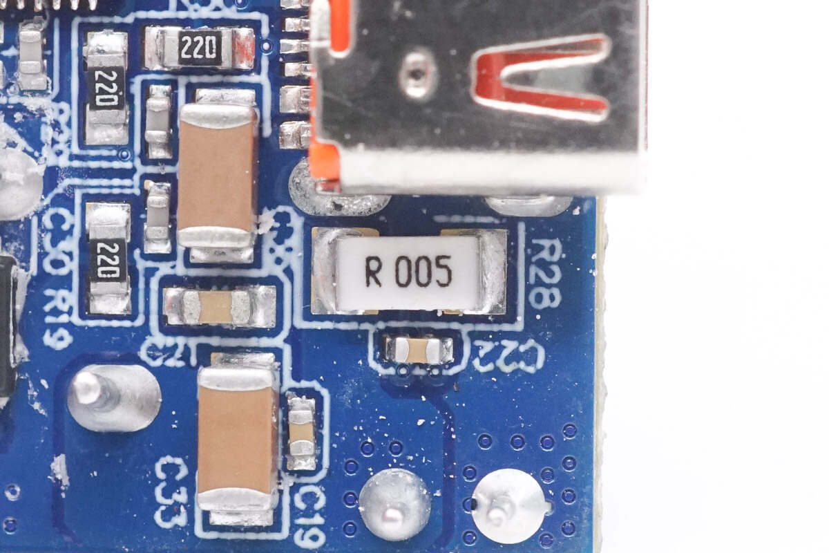
The resistor is used to detect the output current. 5mΩ.
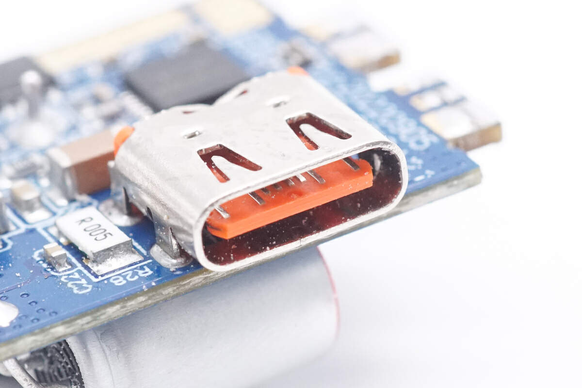
Here is the orange USB-C2 socket.
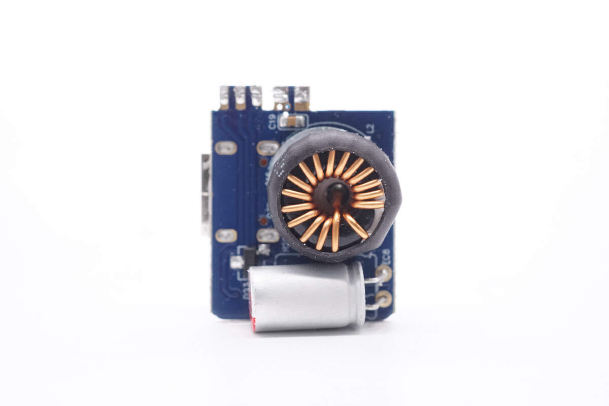
The buck inductor and filter capacitor are on the PCB of USB-C3.
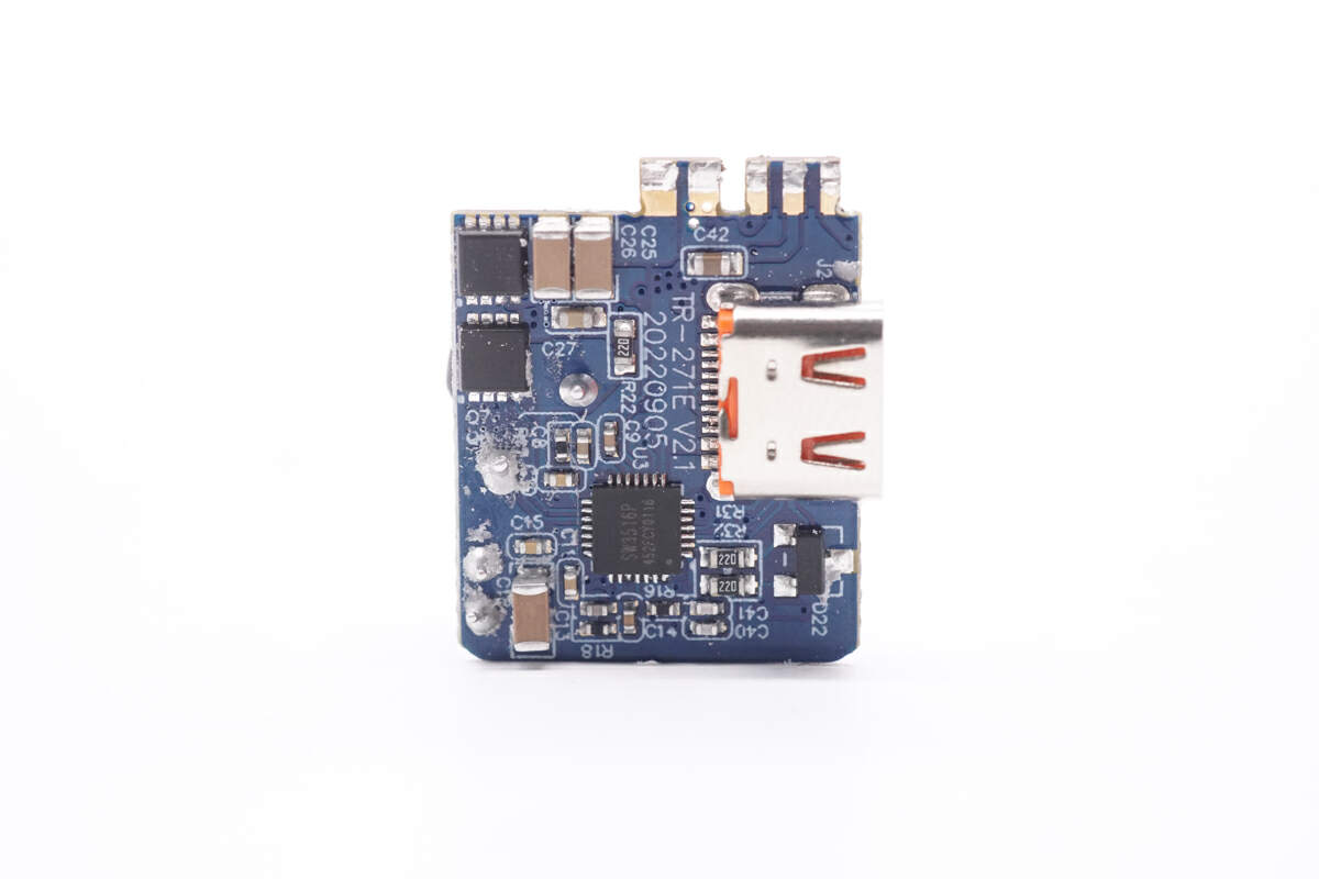
The other side contains the buck protocol chip, synchronous buck MOSFETs, and USB-C socket.
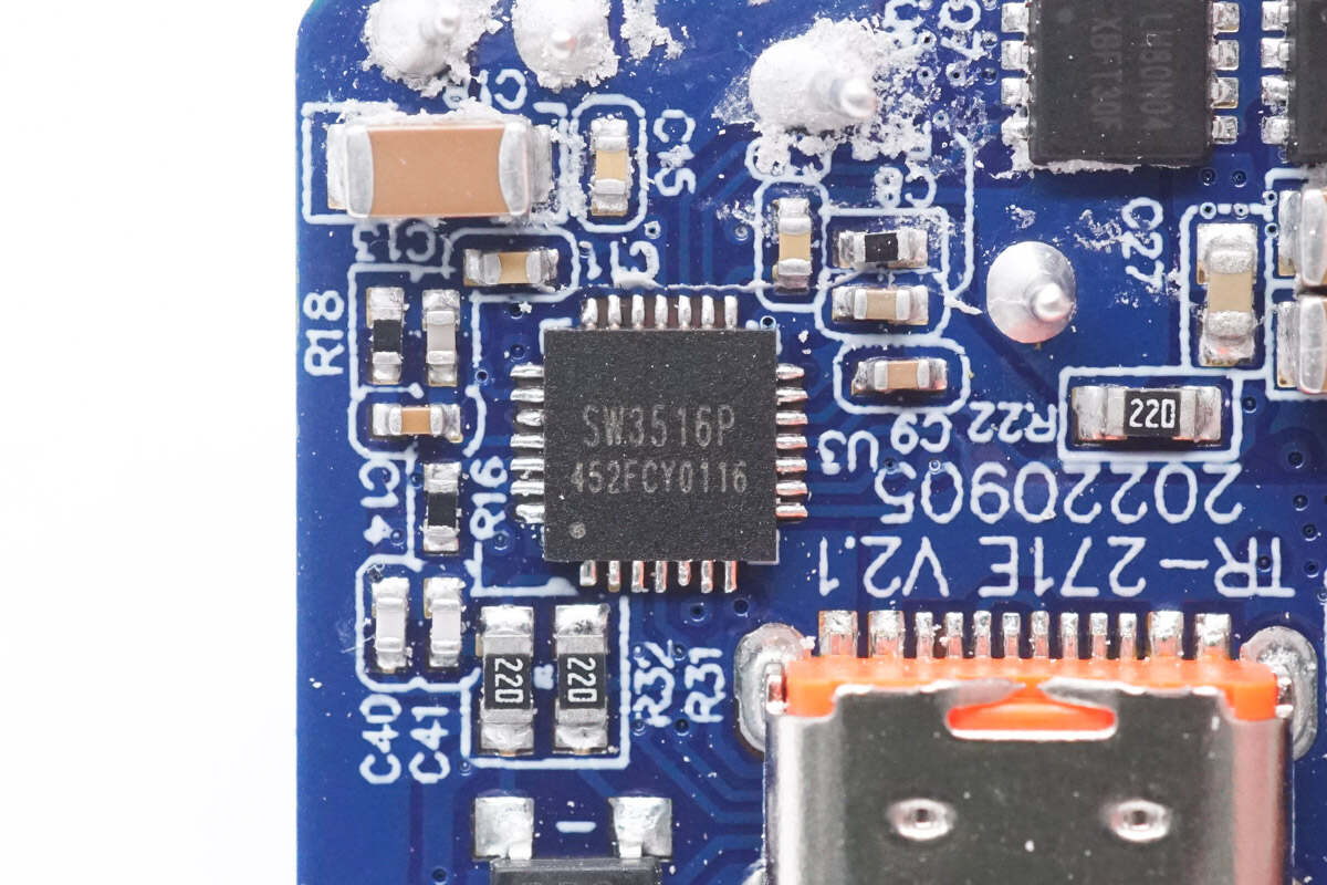
The buck protocol chip is also from iSmartWare, the same as that of the USB-C2. Model is SW3516P.
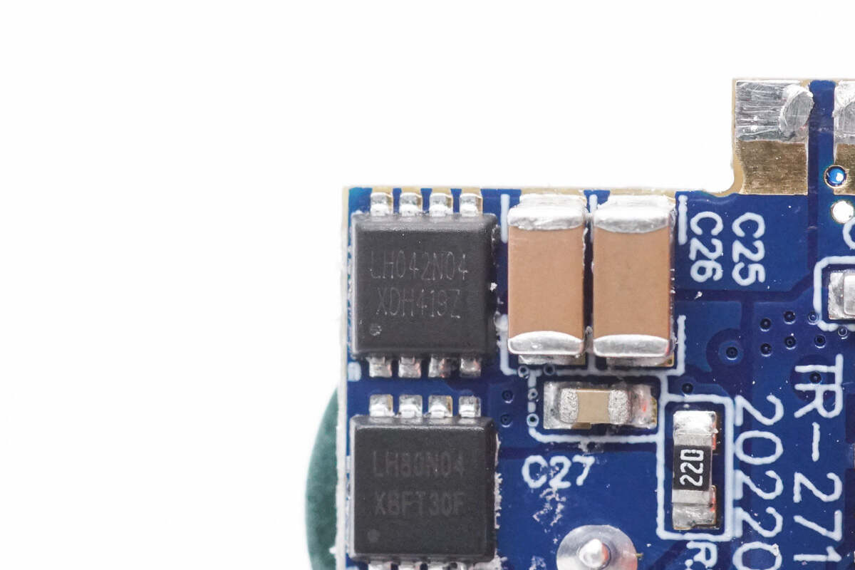
This synchronous buck MOSFET is from LIHOMICRO. Model is LH042N04.
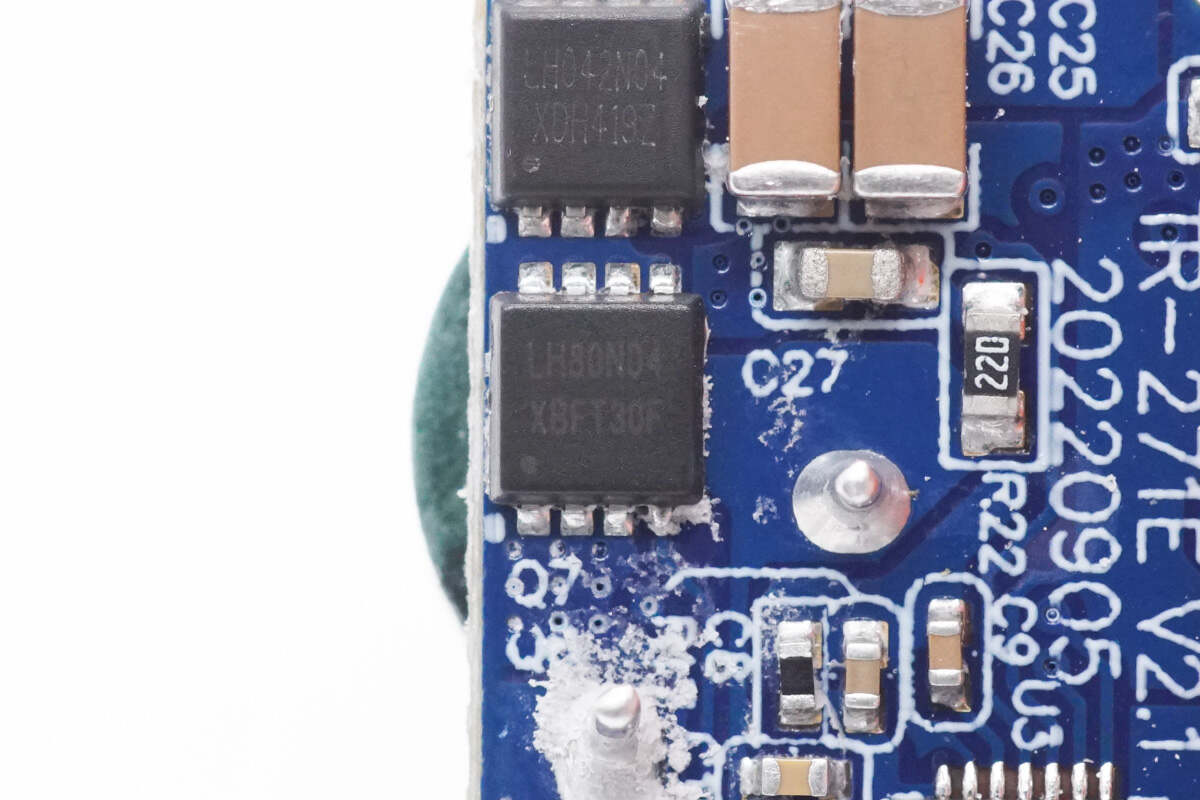
The other synchronous buck MOSFET is also from LIHOMICRO. Model is LH80N04.
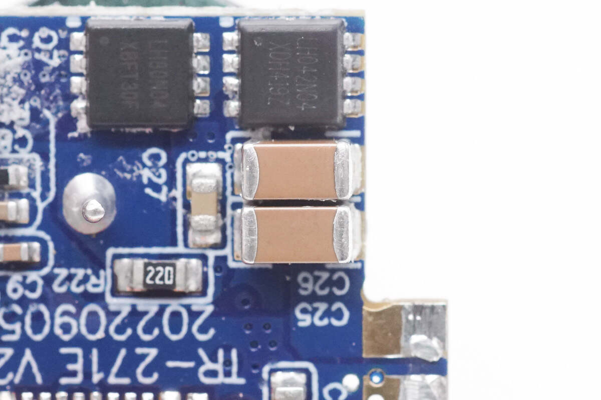
Here are two MLCC capacitors.
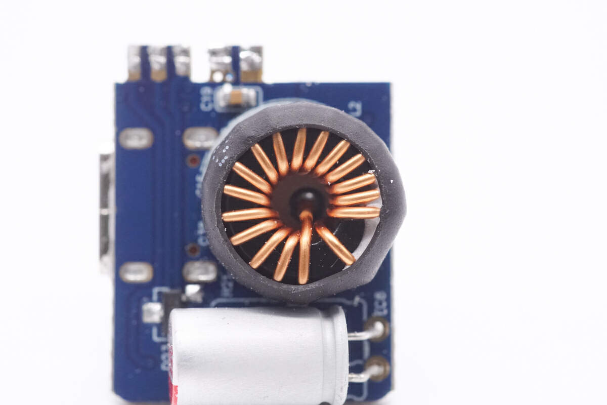
The buck inductor is insulated by heat-shrinkable tubing.
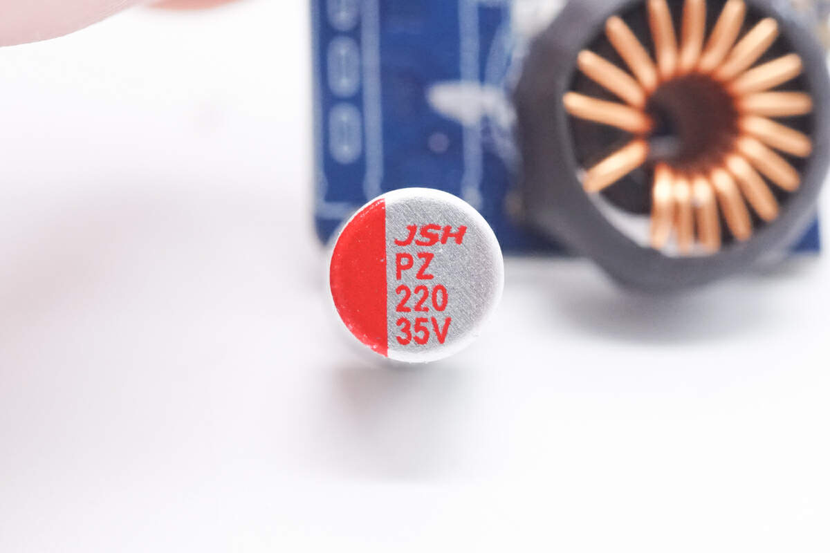
Here is the solid capacitor for output filtering. 220μF 35V.
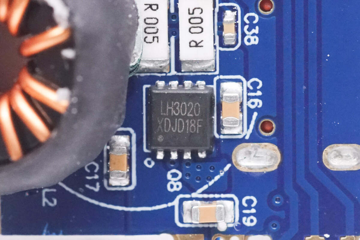
The VBUS MOSFET is from LIHOMICRO and adopts DFN3 x 3 package. Model is LH3020. 30V 8mΩ.
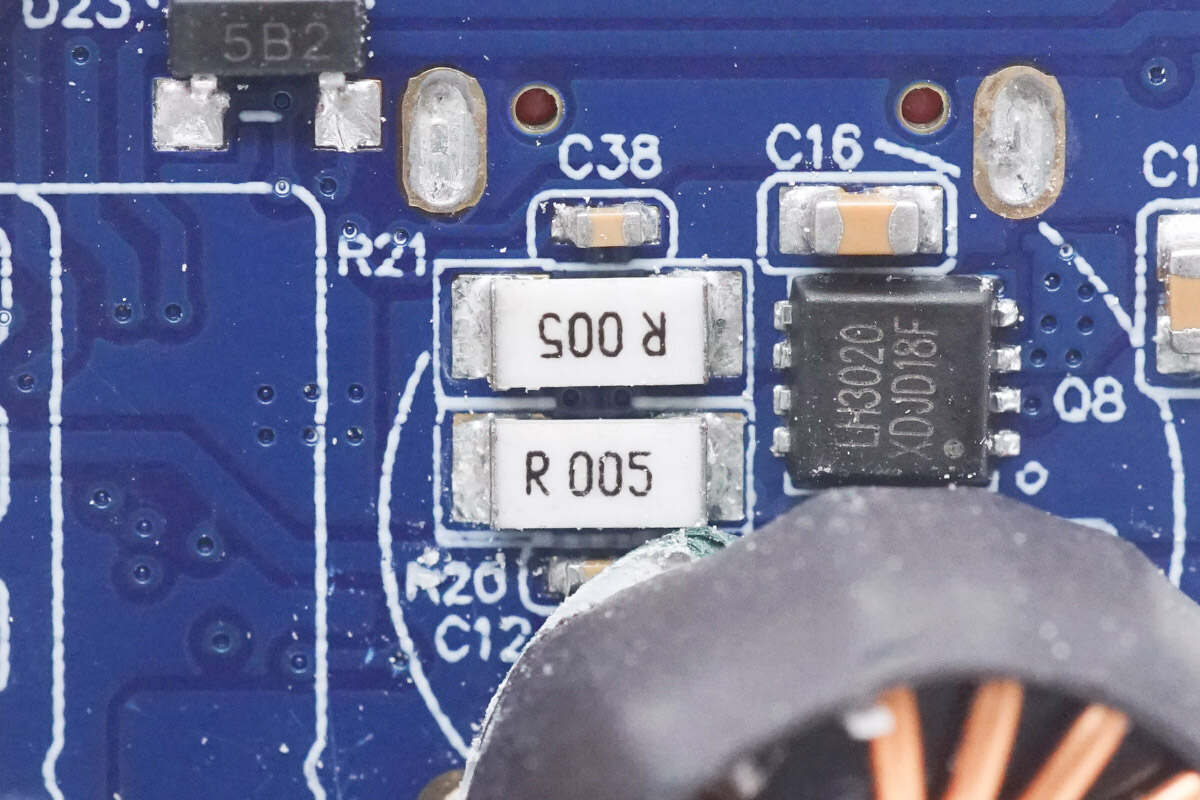
These two resistors are used to detect the current of USB-C and USB-A. 5mΩ for each.
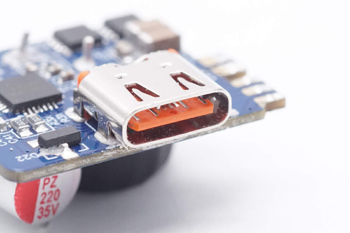
The USB-C3 socket is also orange.
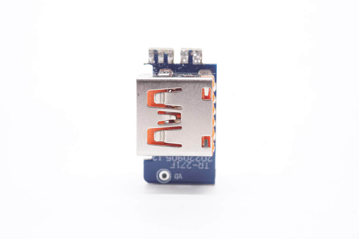
This is the PCB of USB-A.
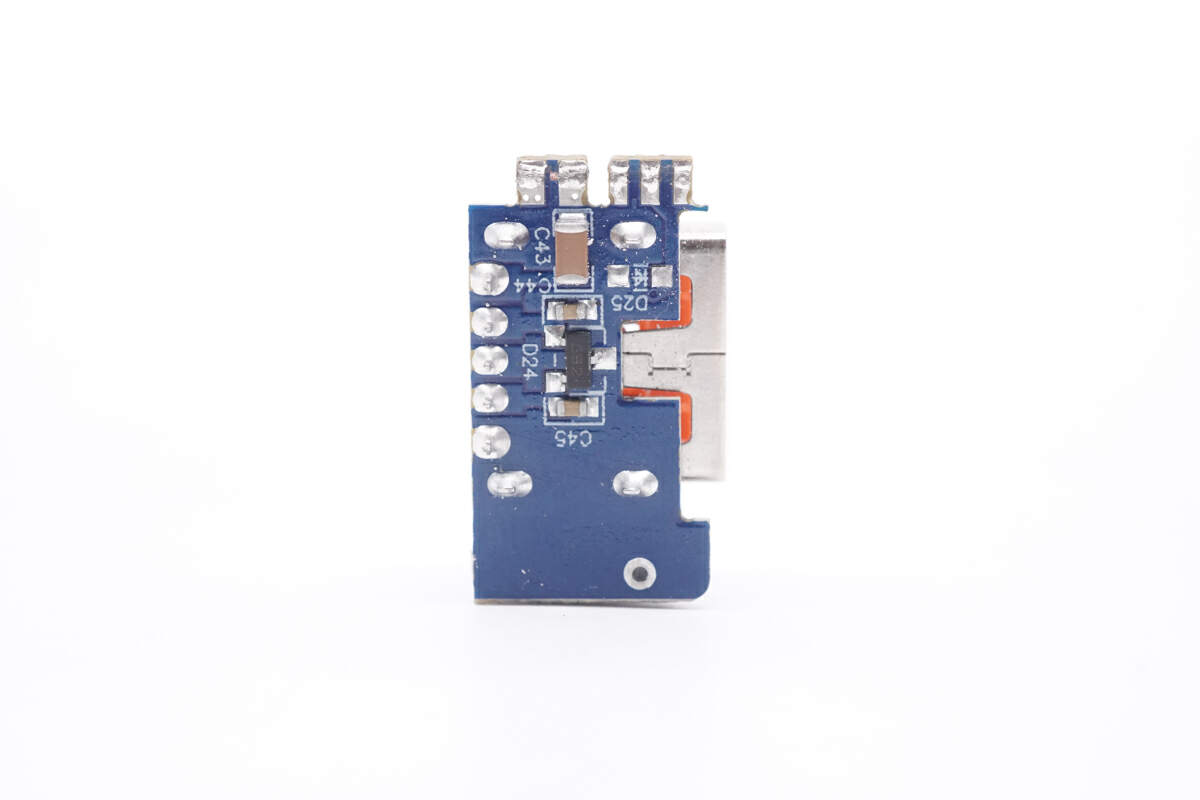
The back of it has a TVS.
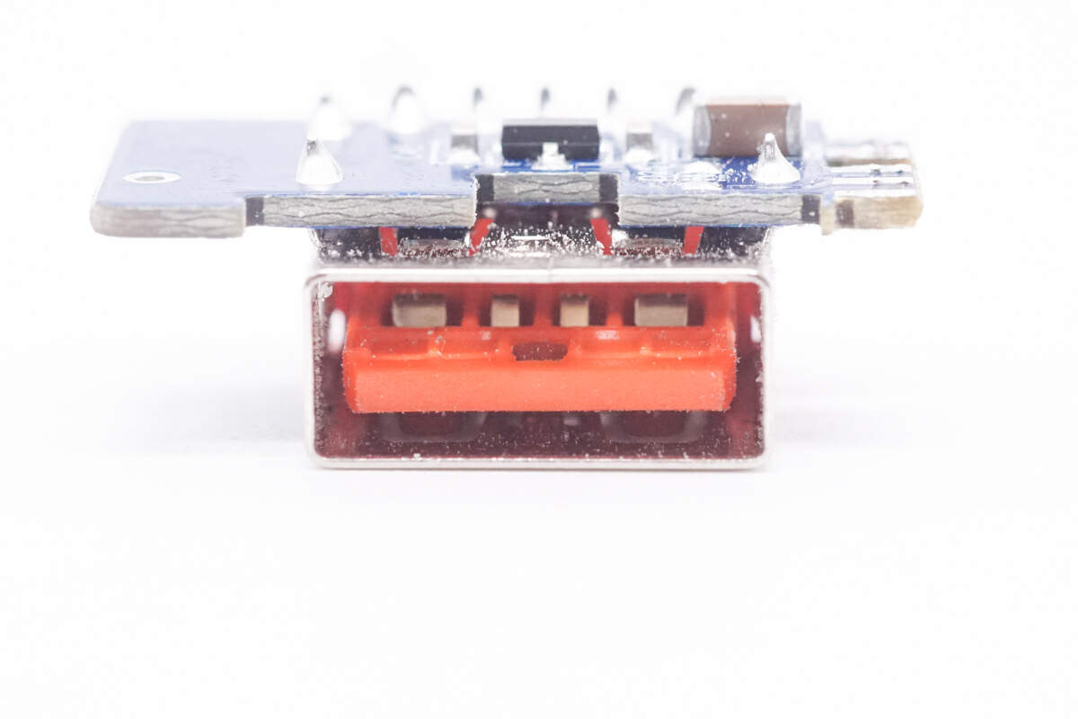
The USB-A socket adopts widened pins for high current.
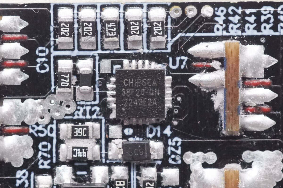
The MCU is from Chipsea. It integrates 12-bit ADC and 8-bit Flash. It also has I²C and UART ports. Model is CSU38F20.
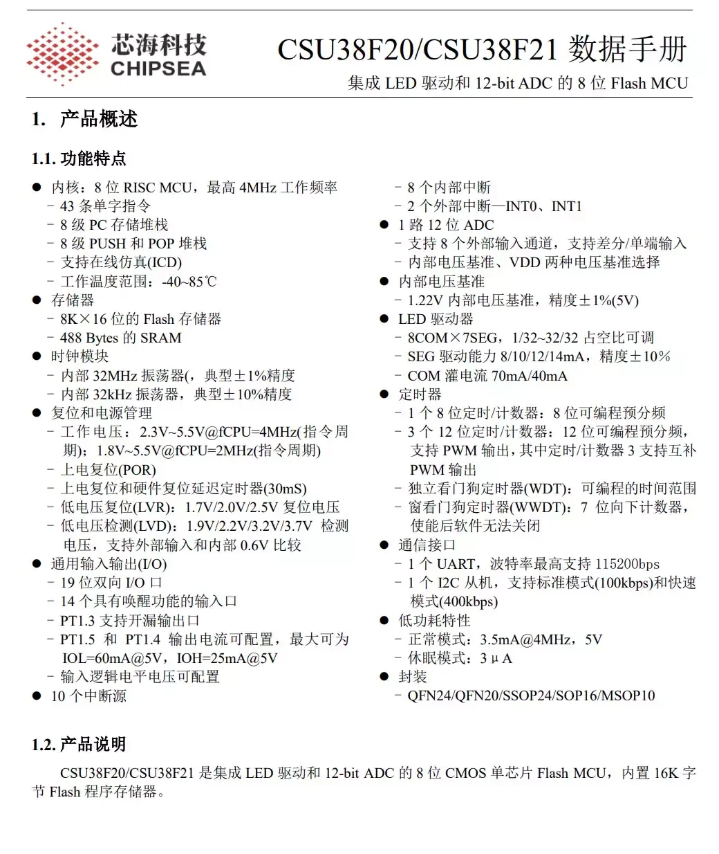
Here is all the information about the Chipsea CSU38F20.
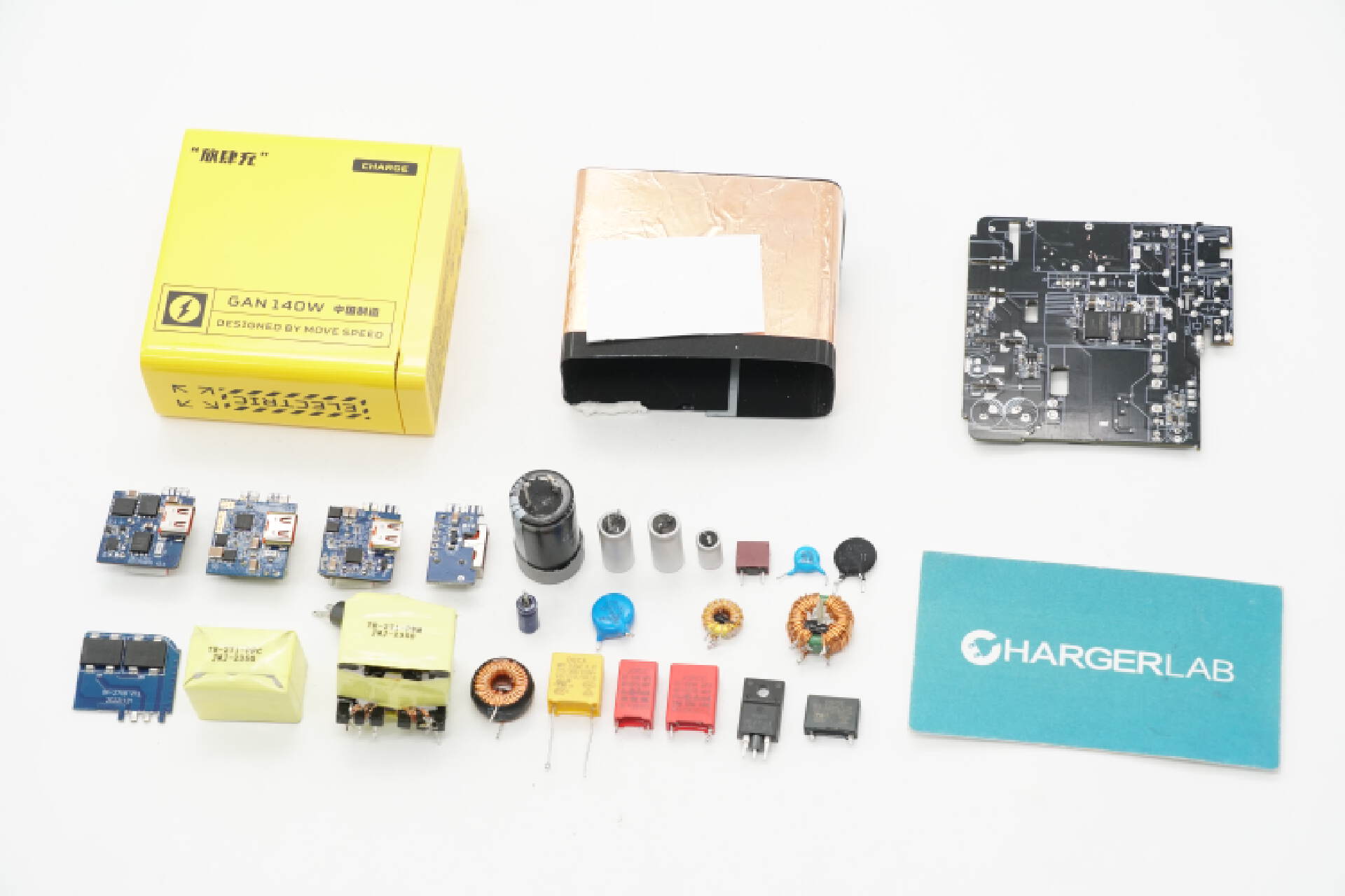
Well, those are all components of the MOVESPEED 140W PD3.1 4-in-1 Charger.
Summary of ChargerLAB
The MOVESPEED 140W PD3.1 charger has a rounded case and a yellow matte surface. It is equipped with four ports and comes with a dual USB-C cable.
After taking it apart, we found it adopts a PFC circuit and flyback topology. It also adopts three independent buck circuits to achieve four-port fast charging and automatic power distribution. The PCBA module is wrapped and insulated with mylar sheets and copper sheets. And it is filled with pounding compound. The internal structure is compact, which effectively saves space. All of these makethe charger smaller than the Apple 140W charger, with even more ports.
Related Articles:
1. PD3.1 | Teardown of Kovol 140W GaN Charger
2. Teardown of UGREEN 65W 3-in-1 Nexode RG GaN Charger (CD361)
3. Teardown of LDNIO 140W GaN 6-in-1 Desktop Charger (A6140C)

