Introduction
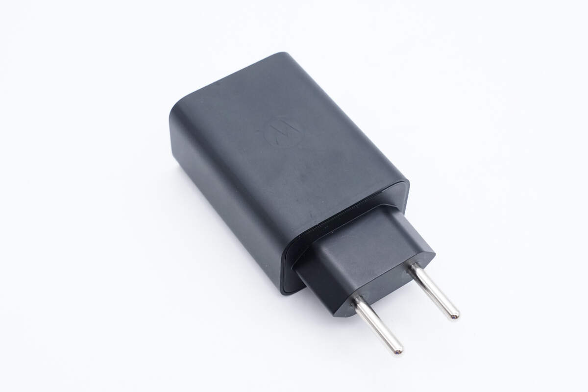
ChargerLAB got a 50W charger from Motorola. The biggest advantage of this charger is that it is equipped with a USB-A and a USB-C port, which can charge two devices at the same time. It looks ordinary and is fitted with a European plug. Next, let's take it apart to see its internal components and structure.
Product Appearance
The charger's shell is frosted and anti-fingerprint.
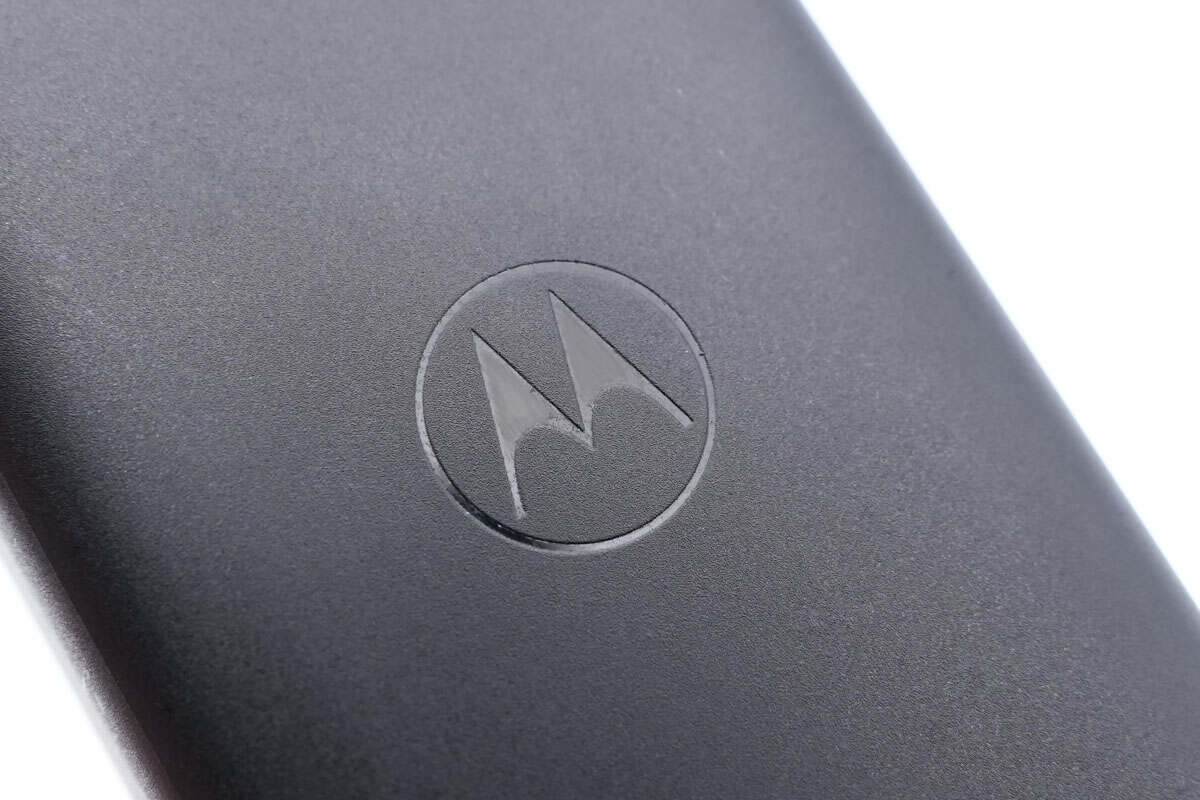
The Motorola logo is engraved on the front.
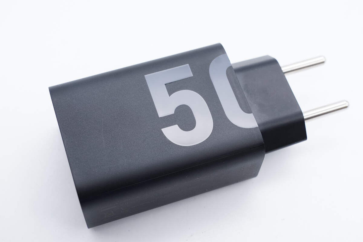
There is a bright 50 on the back, indicating the maximum output power of the charger.
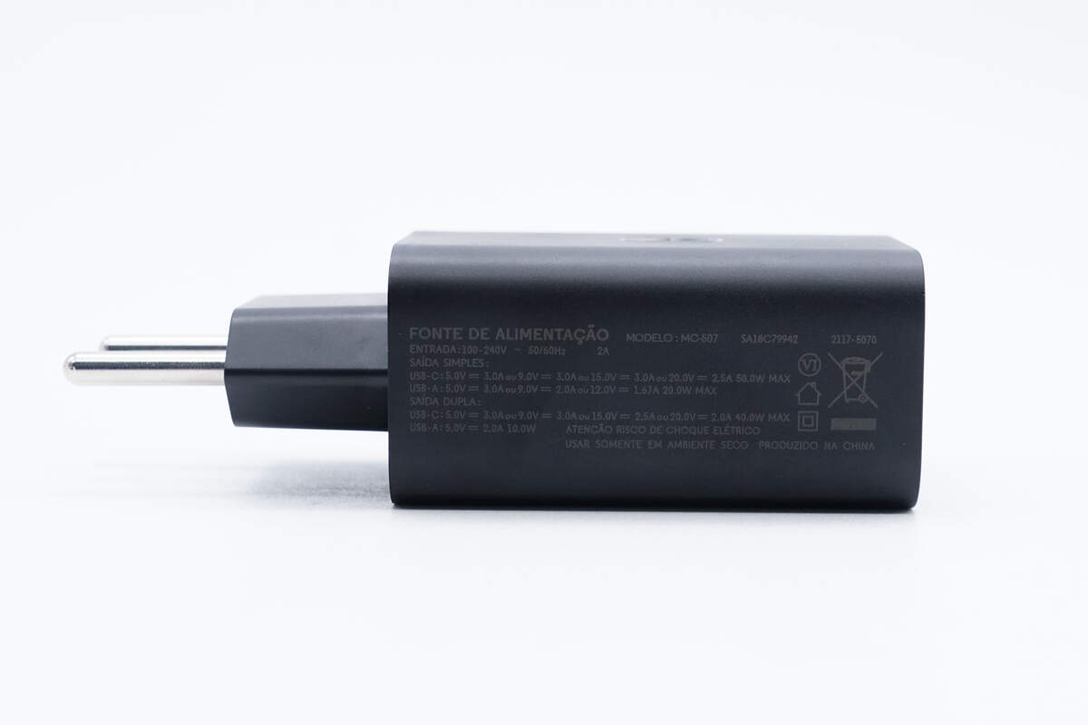
The specs info is printed on the side.
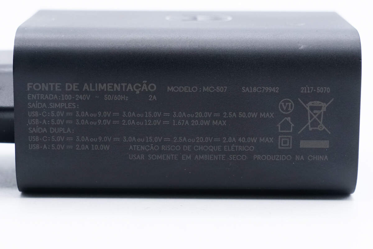
Model: MC-507
Input: 100-240V~50/60Hz 2A
Single Port Output:
USB-C: 5V3A、9V3A、15V3A、20V2.5A 50W MAX
USB-A: 5V3A、9V2A、12V1.67A 20W MAX
Dual Port Output:
USB-C: 5V3A、9V3A、15V2.5A、20V2A 40W MAX
USB-A: 5V2A 10W MAX
It has passed Level VI energy efficiency certification.
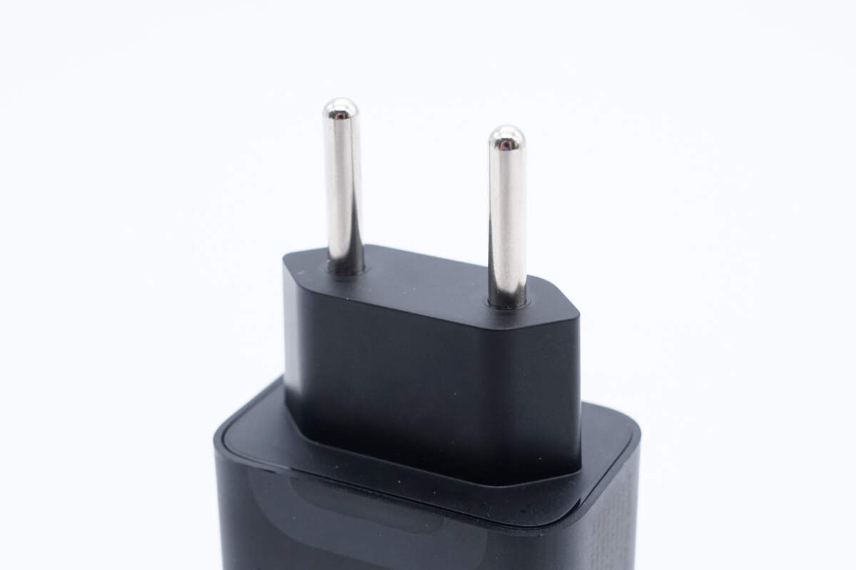
Here is the European plug.
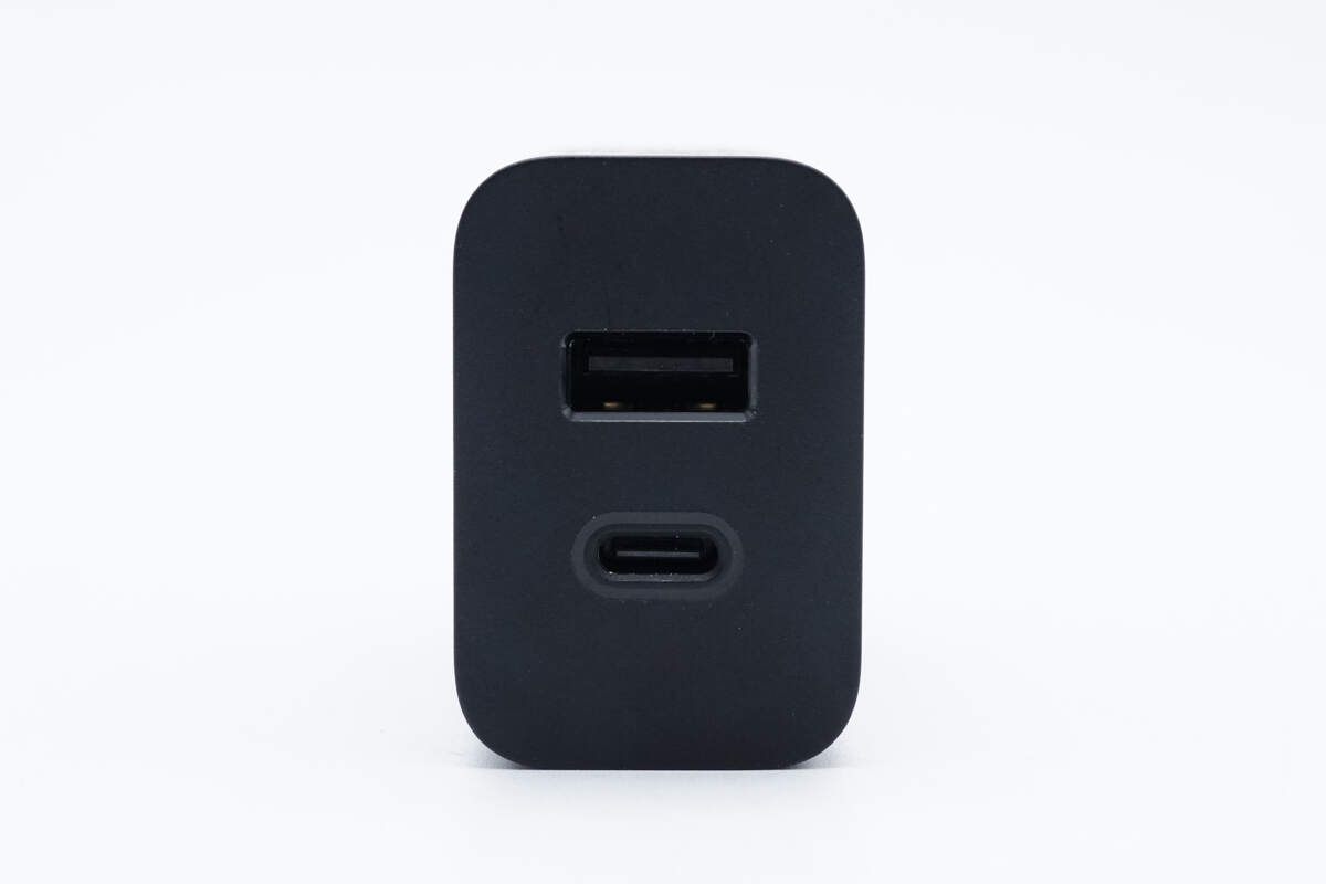
The plastic sheets of the USB-A and USB-C ports are black.
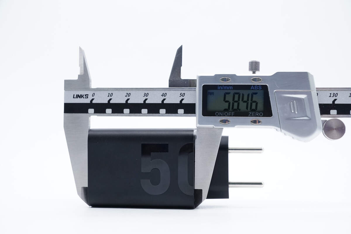
The length is about 58.46 mm (2.3 inches).
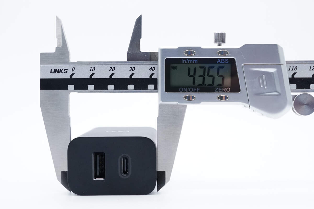
The width is about 43.55 mm (1.71 inches).
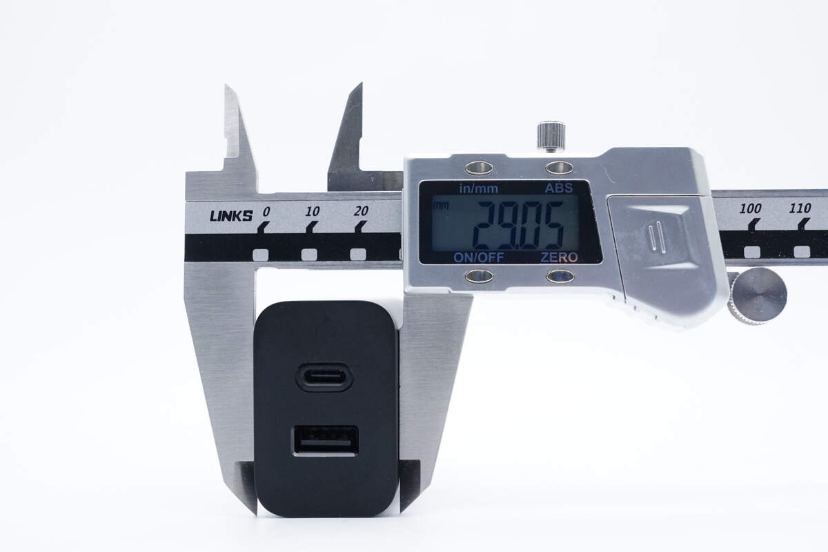
The thickness is about 29.05 mm (1.14 inches).
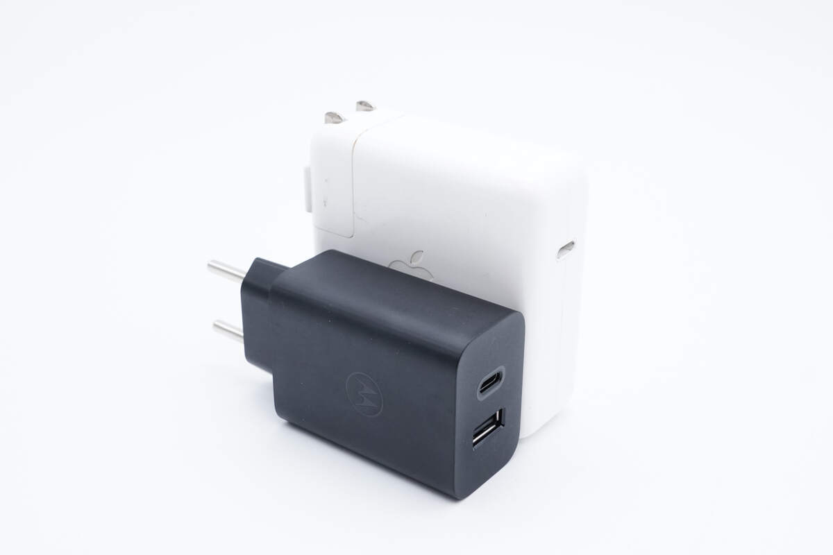
It is much smaller than the Apple 61W charger.
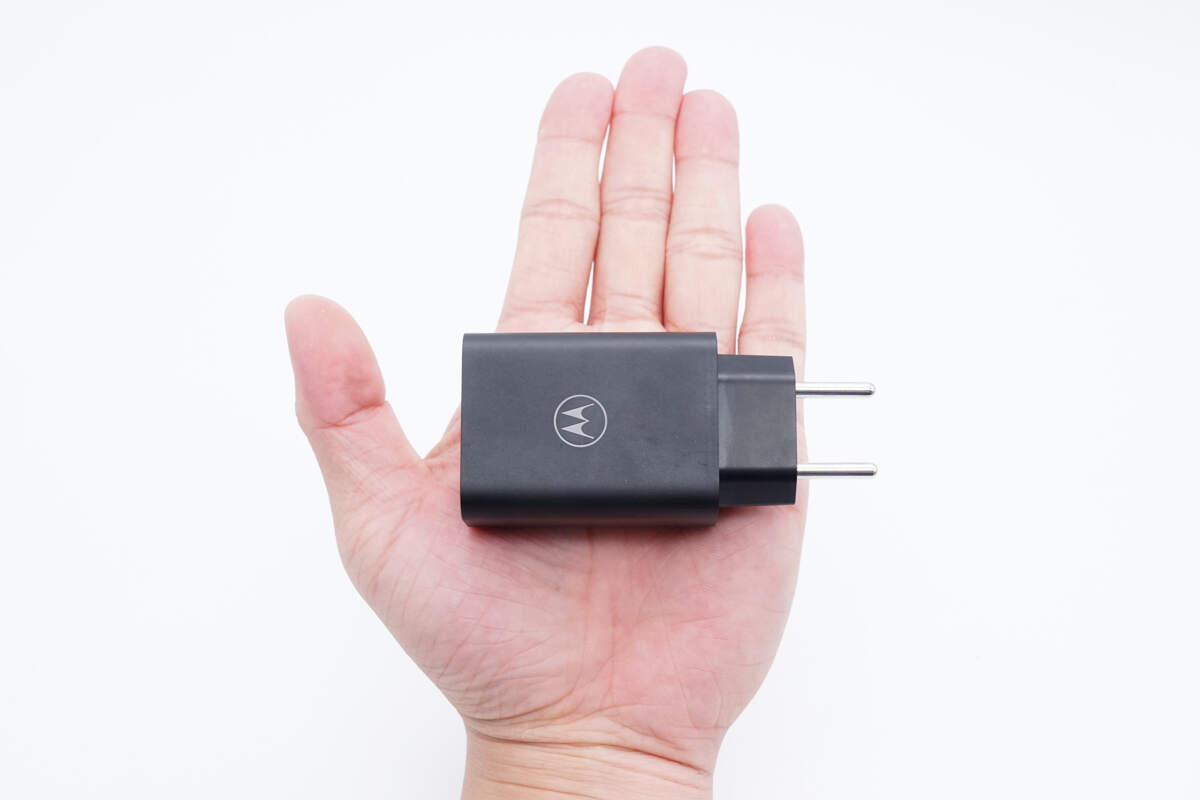
That's how big it is in the hand.
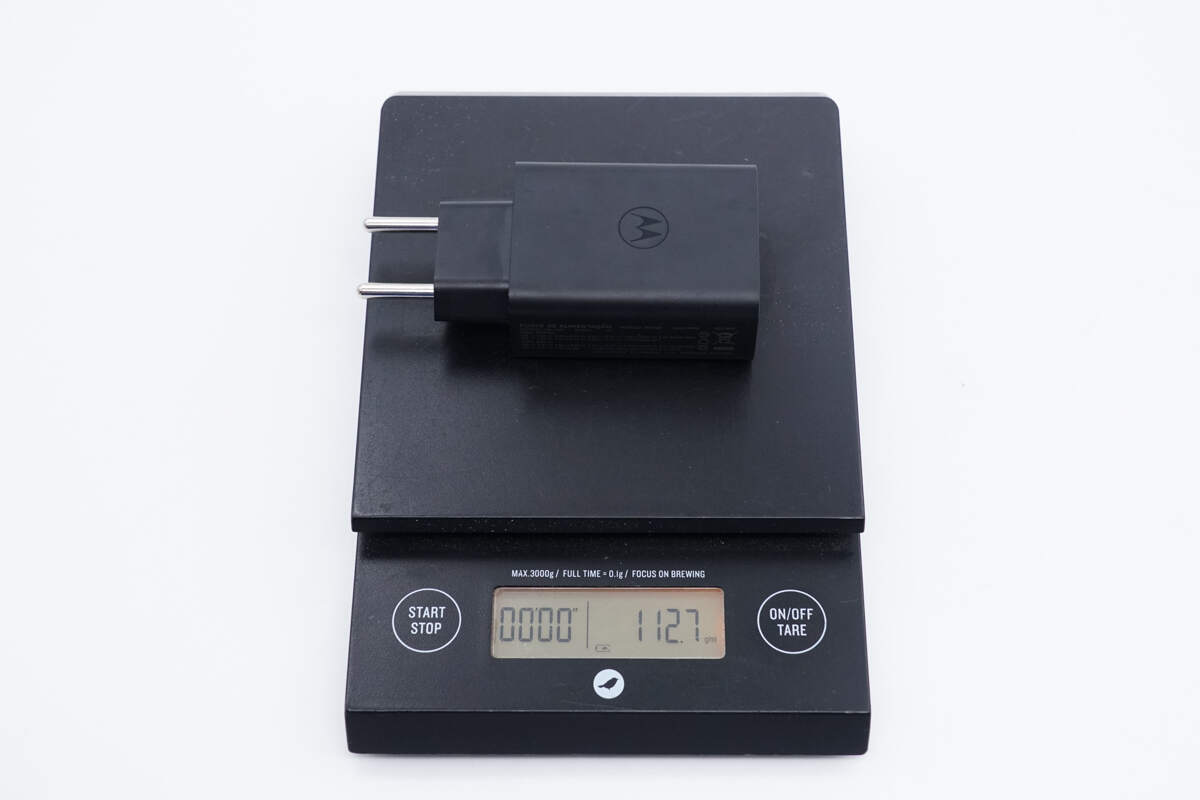
The weight is about 112.7 g (3.98 oz).
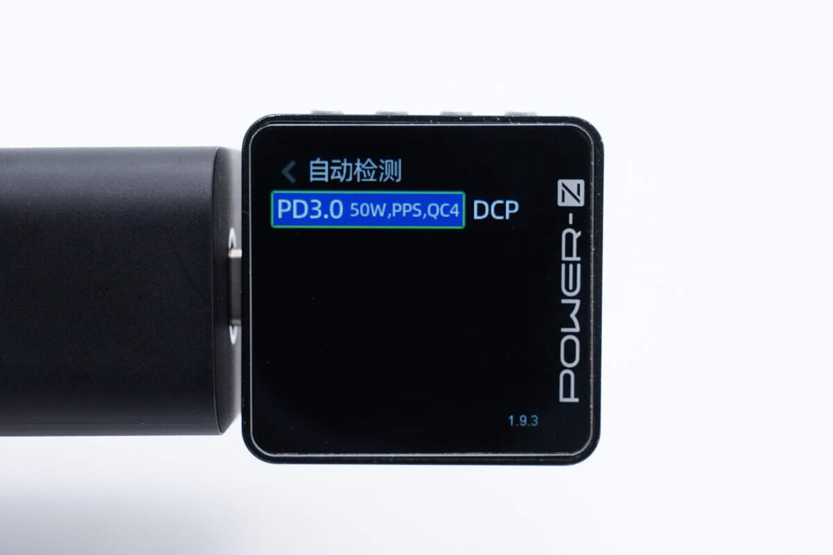
ChargerLAB POWER-Z KM003C shows the USB-C port can support PD3.0, PPS, QC4, and DCP charging protocols.
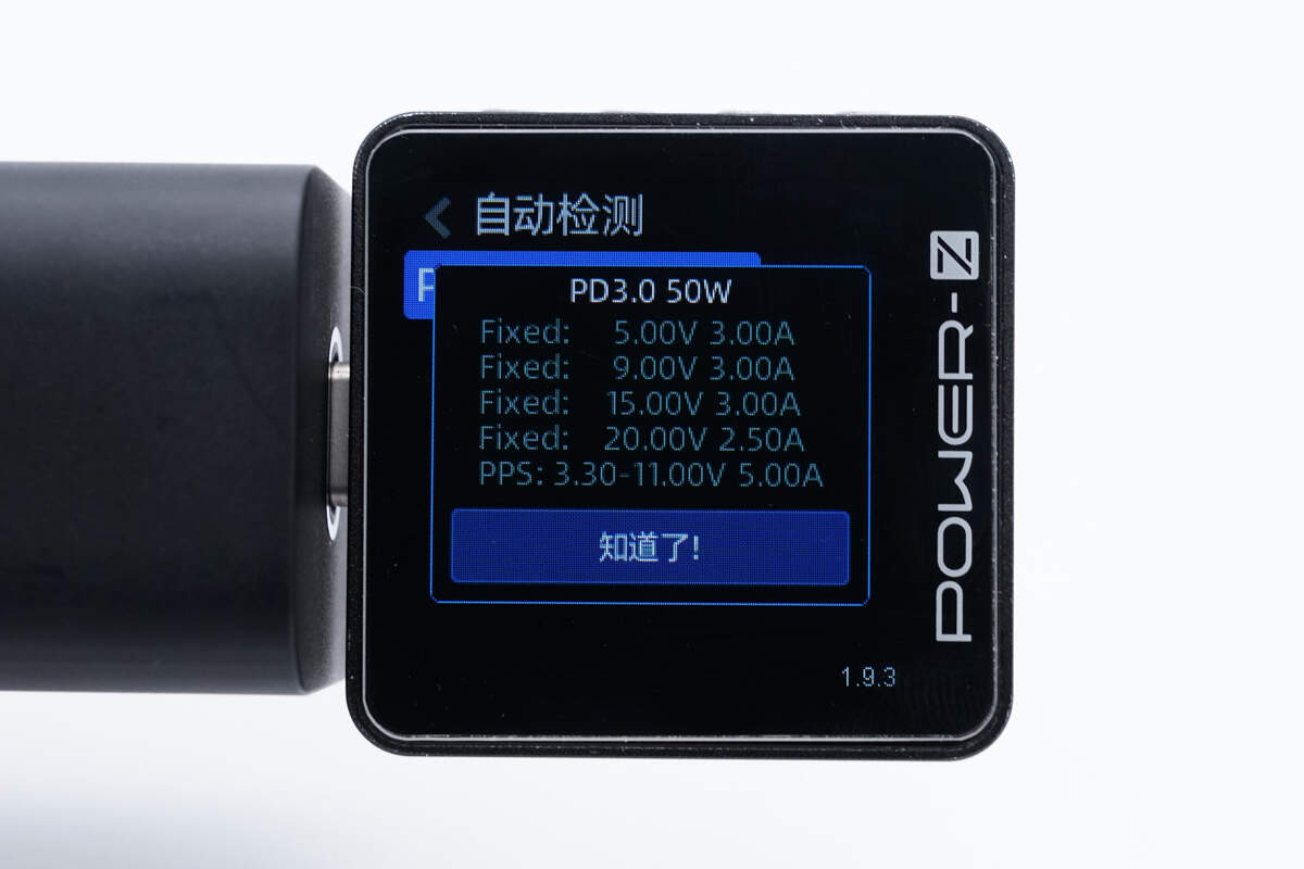
And it has four fixed PDOs of 5V3A, 9V3A, 15V3A, 20V2.5A, and a set of PPS, which is 3.3-11V5A.
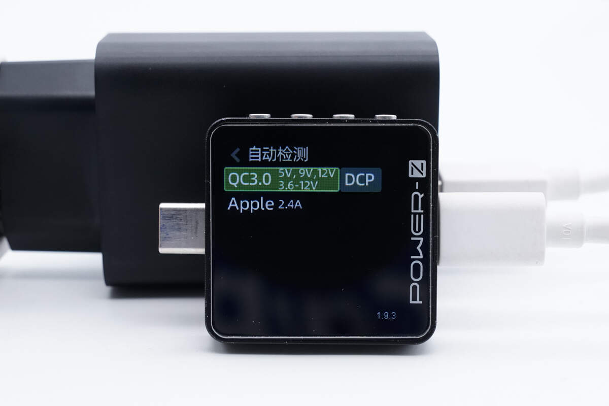
Our tester shows the USB-A port can support QC3.0, DCP, and Apple 2.4A charging protocols.
Teardown
Next, let's take it apart to see its internal components and structure.
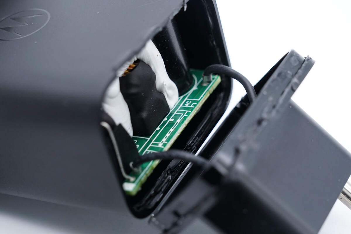
First, pry along the gap to open the input cover. The PCBA module is connected to the plug through wires.
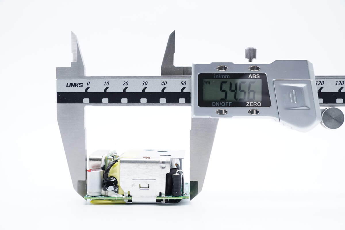
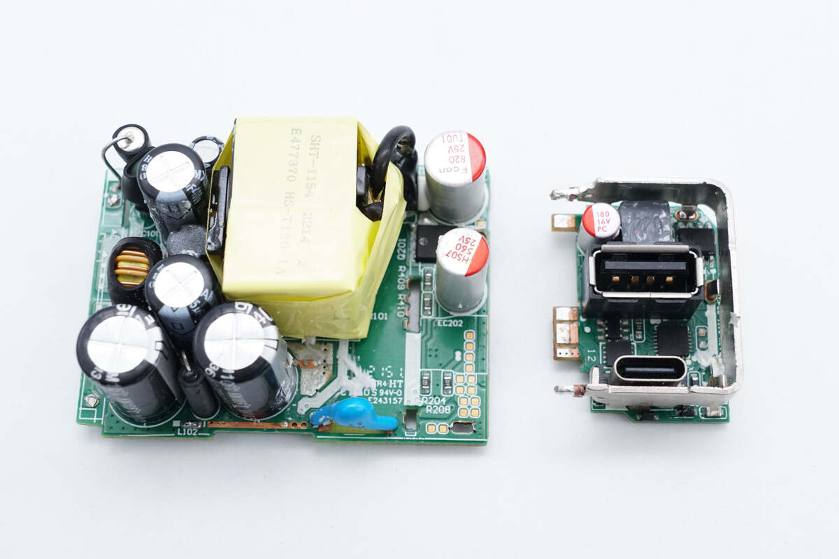
Remove the PCBA module. Its length is about 54.56 mm (2.15 inches).
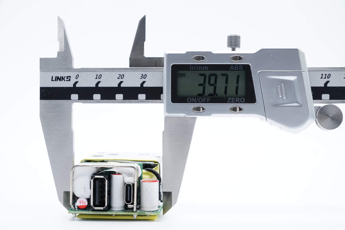
The width is about 39.71 mm (1.56 inches).
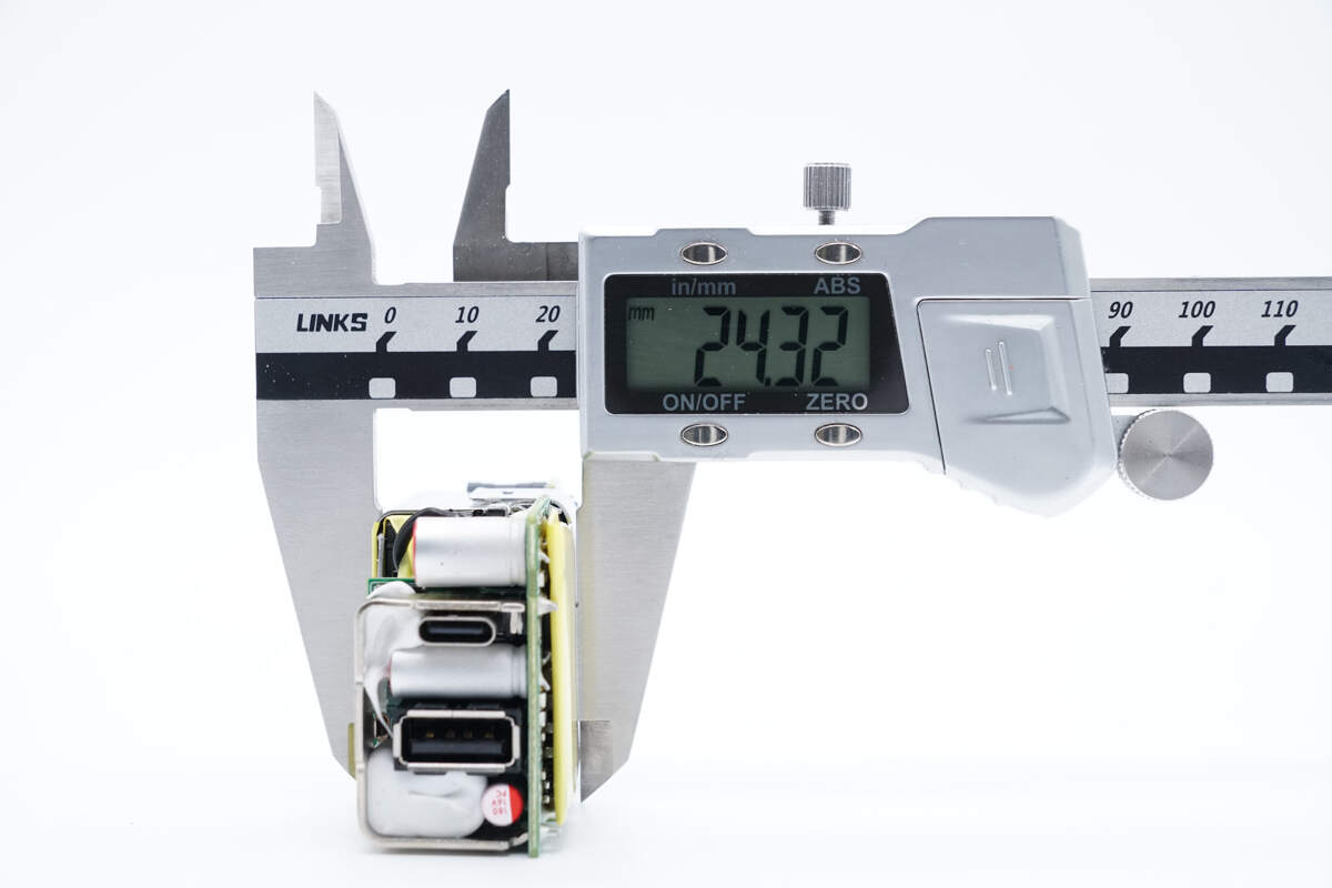
The thickness is about 24.32 mm (0.96 inches).
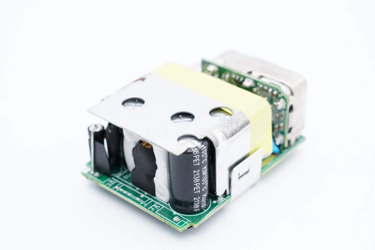
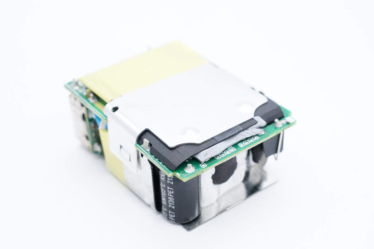
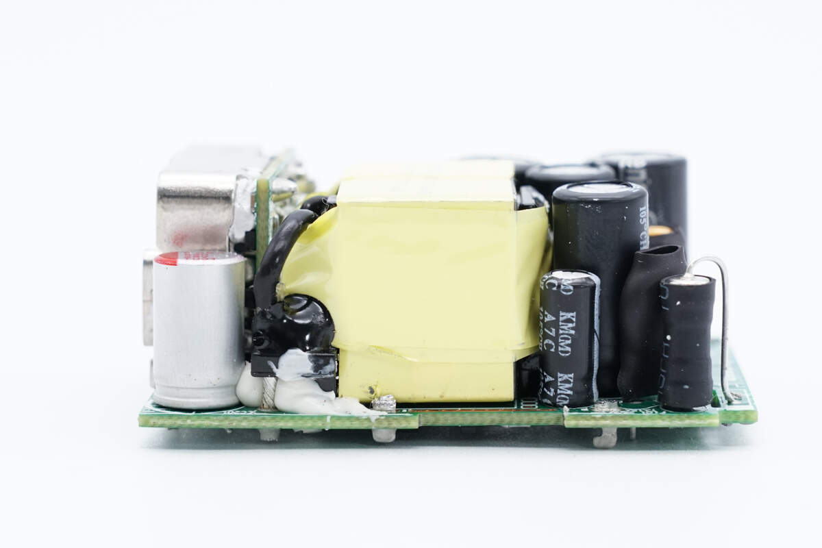
The PCBA module is wrapped with heat sinks, and the gaps between components are filled with potting compounds for reinforcement.
There is a Mylar sheet between the heat sink and the PCB on the back for insulation.
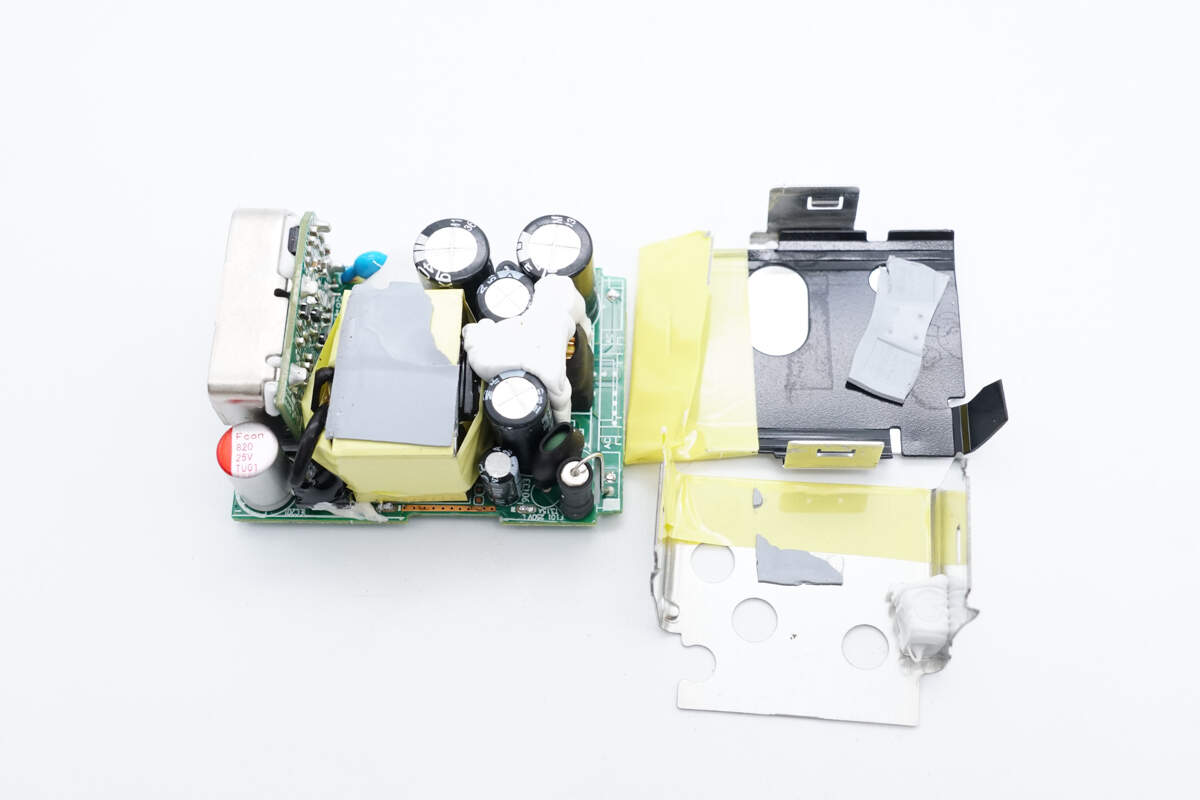
Remove the heat sinks and there is a thermal pad on the transformer.
There is also a thermal pad on the area corresponding to the bridge rectifier and the master control chip to help with heat conduction.
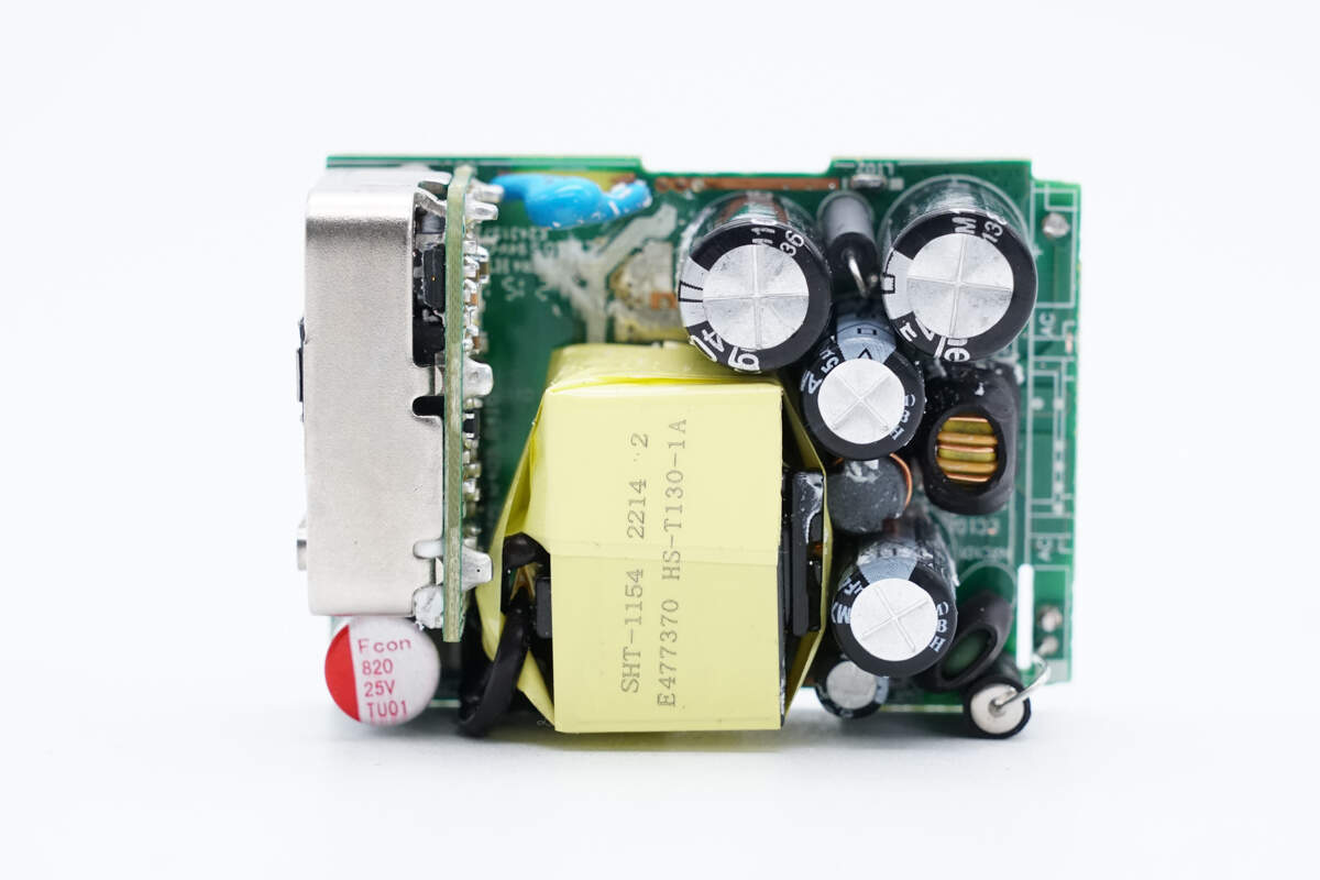
The input end has an NTC thermistor, a common mode choke, electrolytic capacitors, and other components. The output end has a separate small PCB.
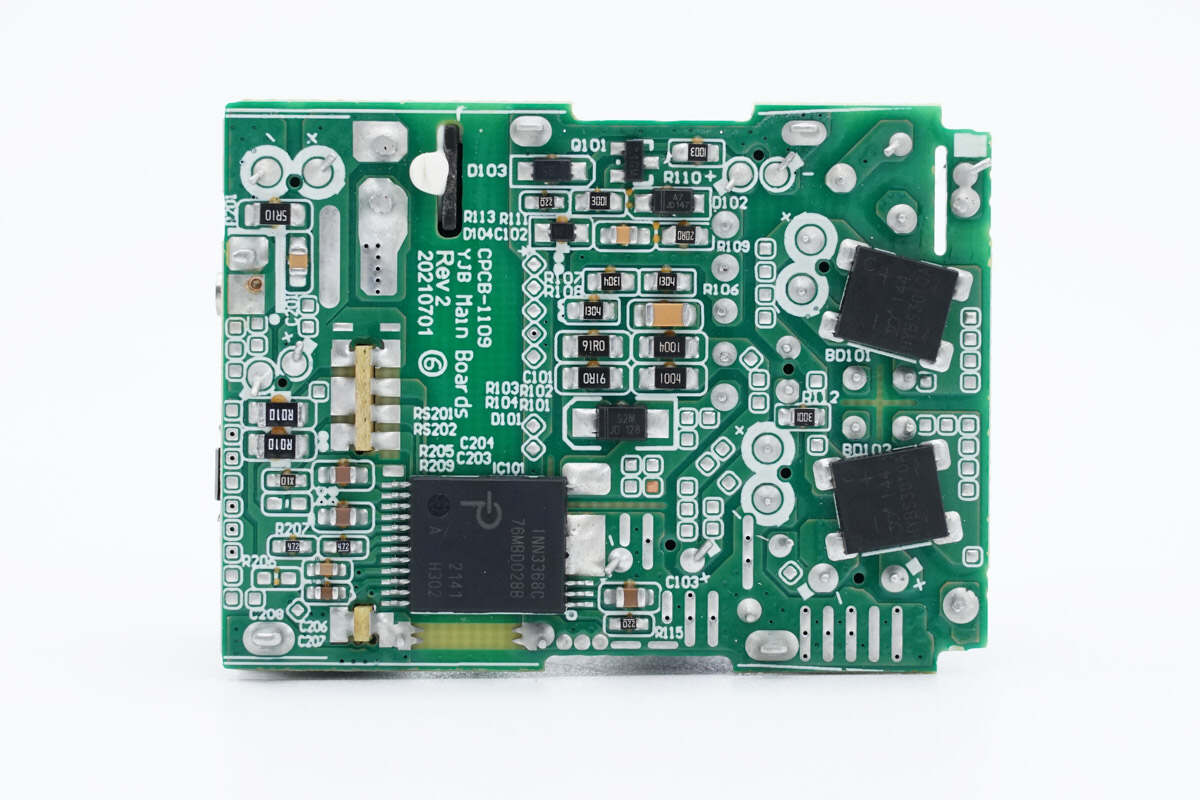
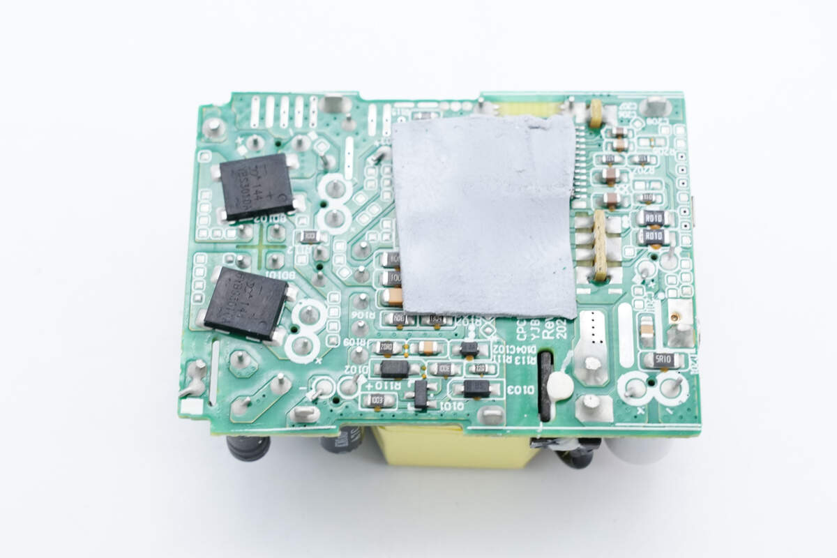
There are two bridge rectifiers and a master control chip on the back.
The fuse, NTC thermistor, and common mode choke are all insulated by heat-shrinkable tubing.
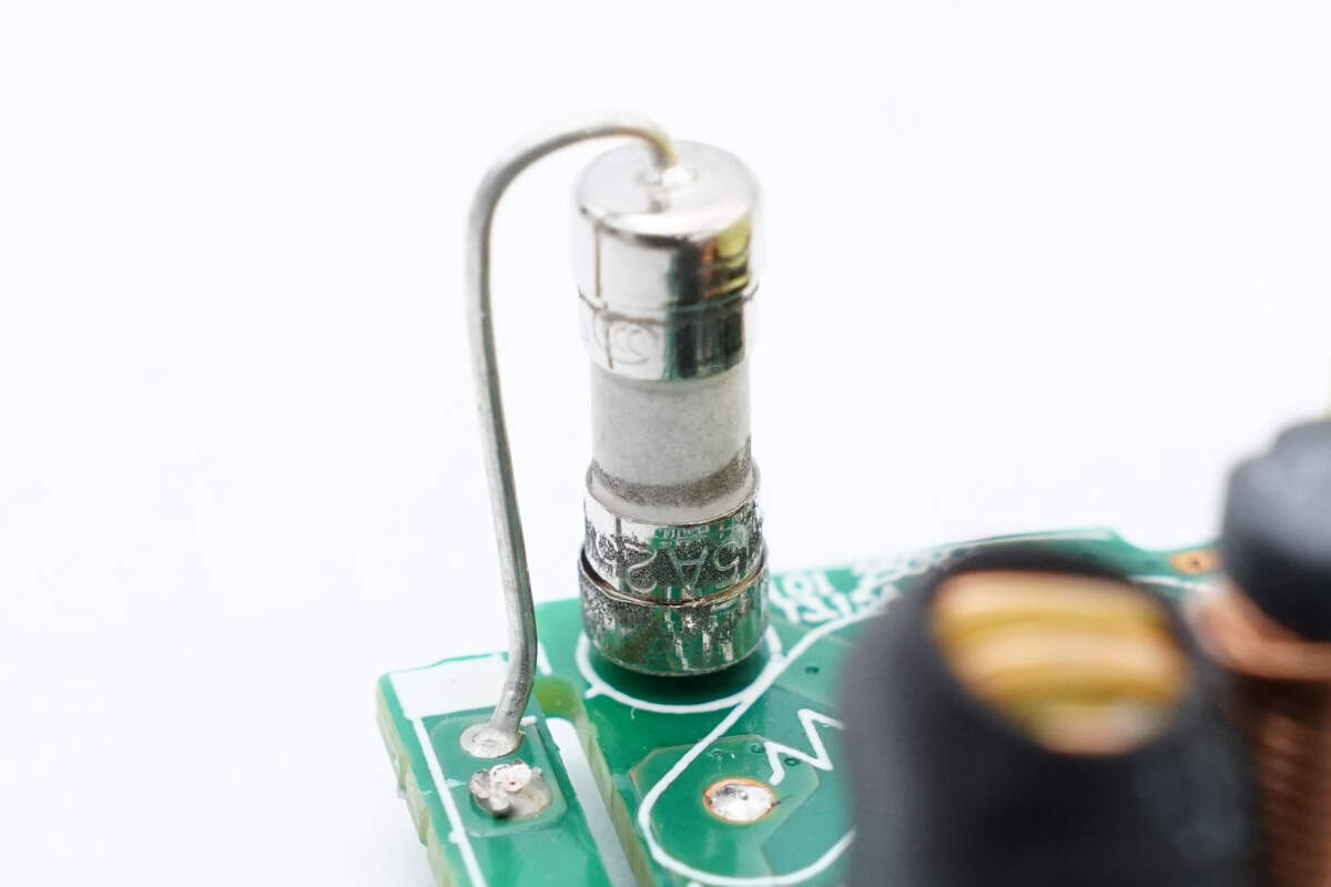
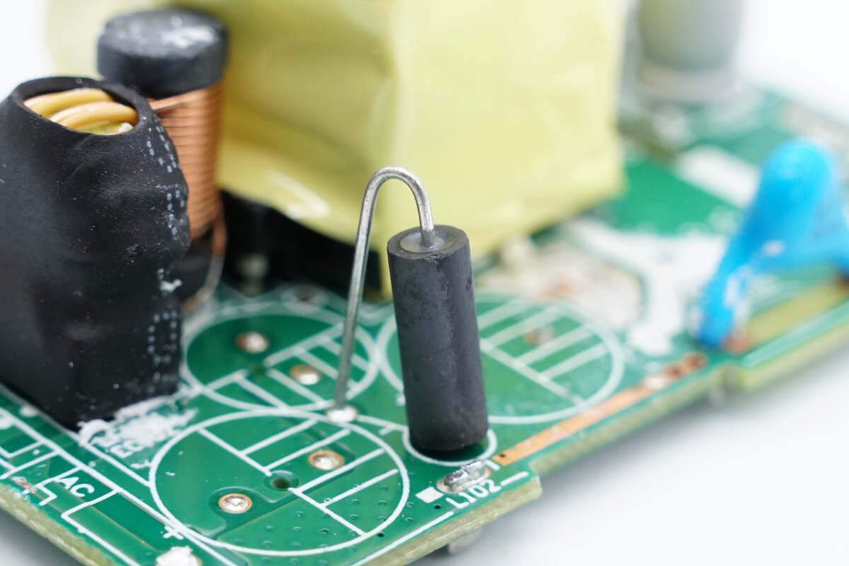
Here is the fuse. 5A 250V.
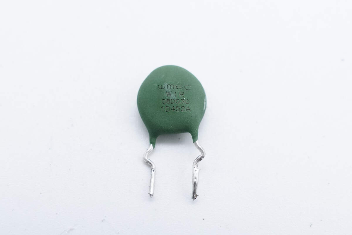
The green NTC thermistor is used to suppress the power-on surge current.
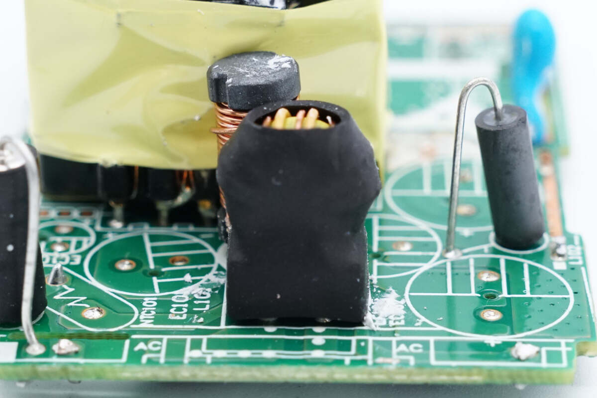
The common mode choke is used to filter out EMI interference.
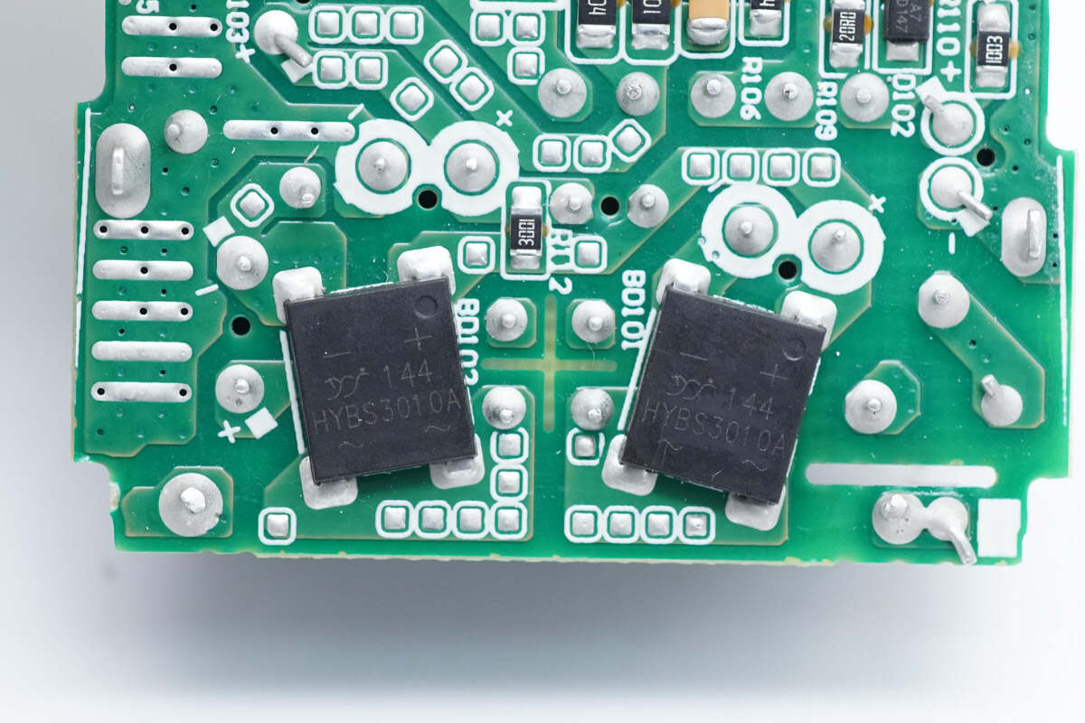
These two bridge rectifiers are from YJ and adopt the YBS package. 3A 1000V. Model is HYBS3010A.
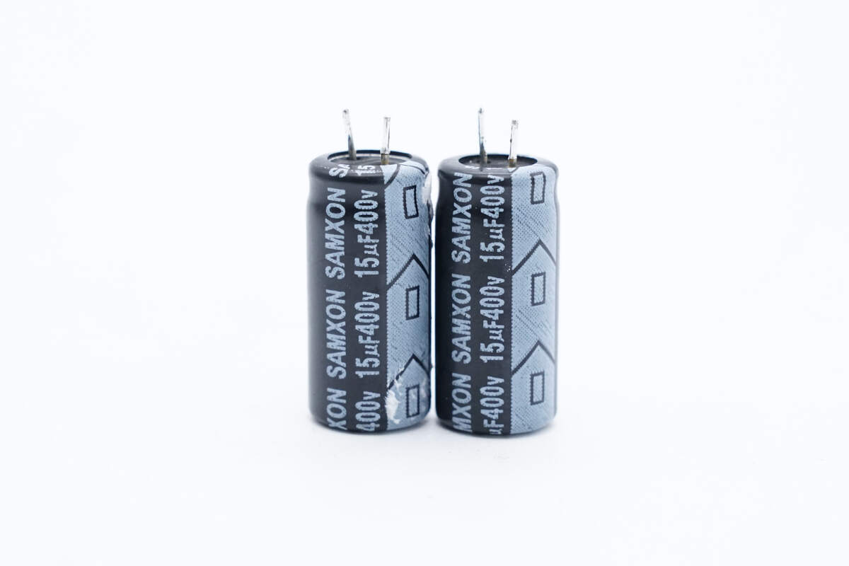
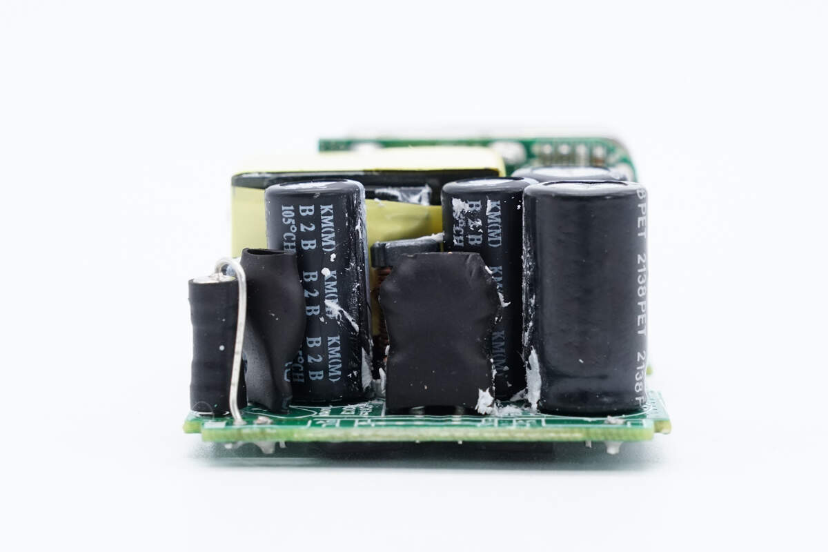
These two electrolytic capacitors are from SAMXON. 15μF 400V.
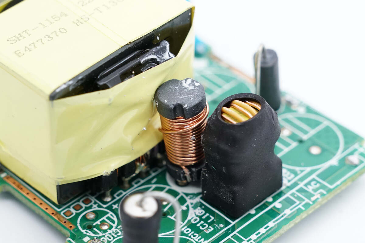
This is the I-shaped filter inductor.
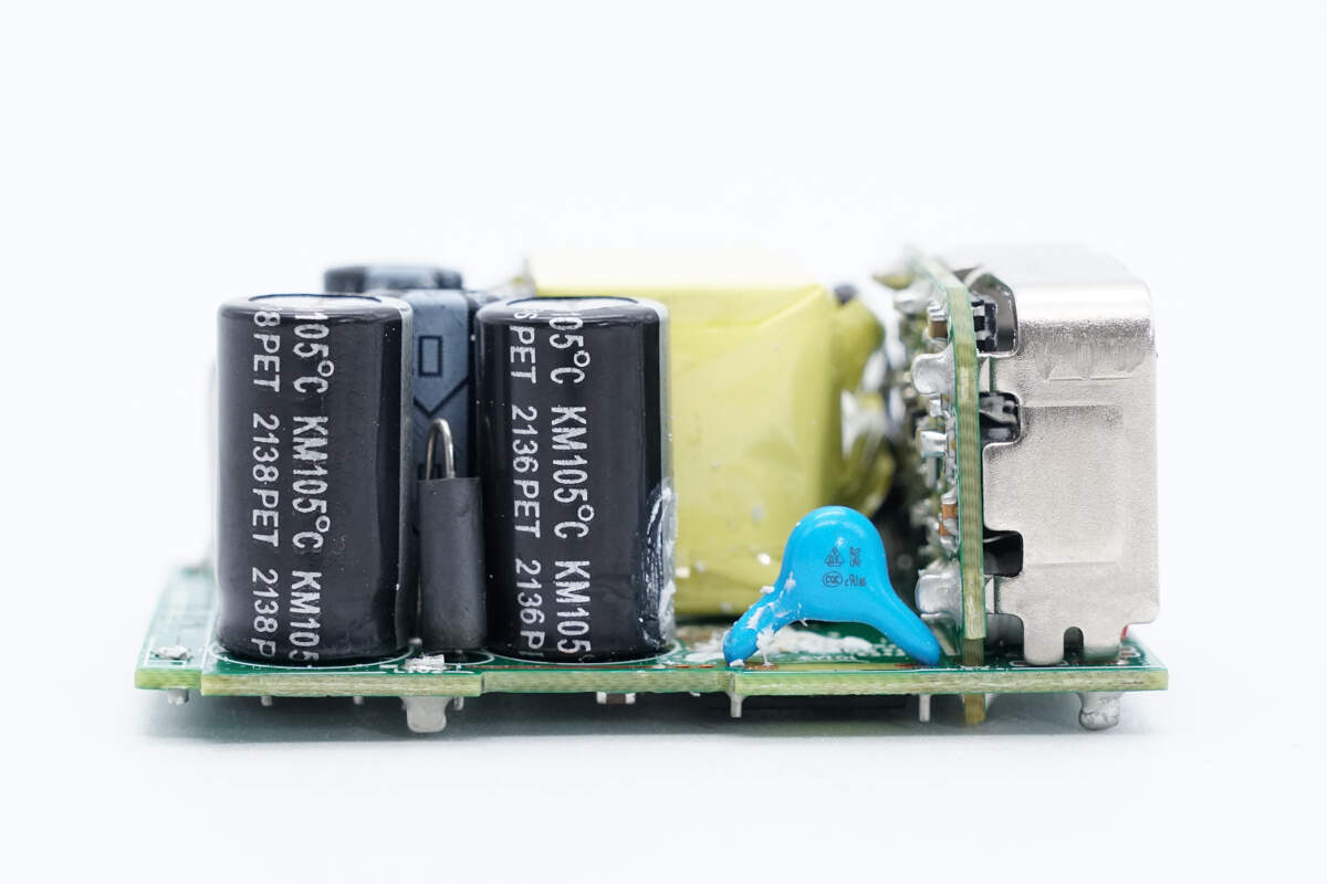
This side also has two electrolytic capacitors, a ferrite bead, and a blue Y capacitor.
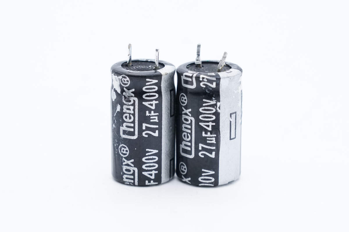
These two electrolytic capacitors are from ChegnX. 27μF 400V.
The ferrite bead is used to suppress high-frequency interference.
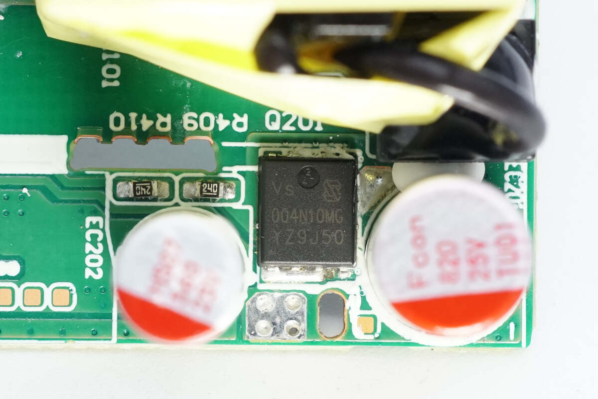
On the other side of the PCB there is a capacitor that powers the master control chip, a transformer, and a synchronous rectifier solid capacitor.
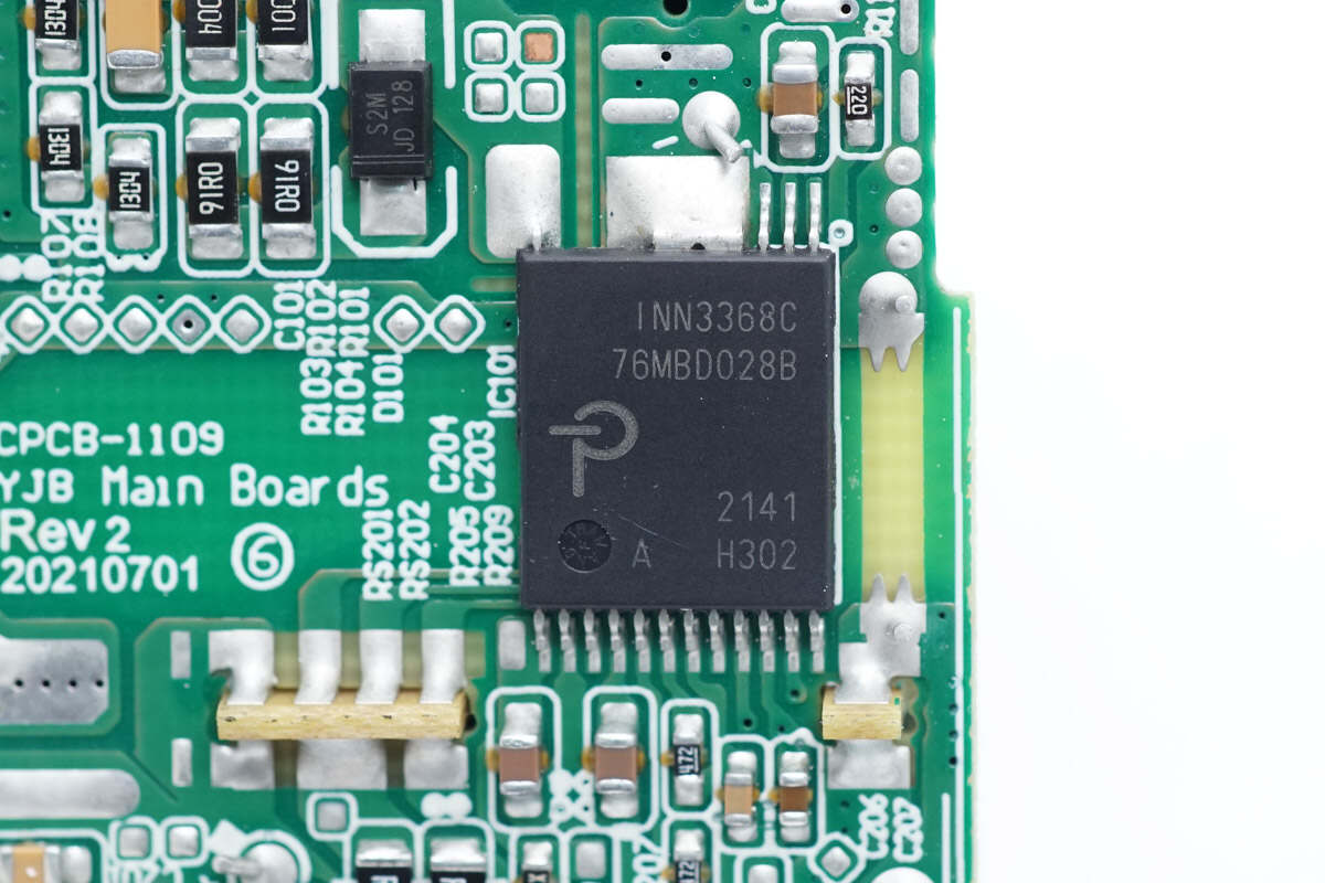
The master control chip is from PI. It is the InnoSwitch3-Pro series, a digitally controlled constant voltage/constant current offline flyback quasi-resonant switch IC that integrates a high-voltage switch, synchronous rectification, and FluxLink feedback functions, with a very high integration level. It is suitable for high-efficiency USB PD 3.0 + PPS/QC adapters. Under a wide voltage range, it can output 50W power in a sealed housing and can output higher power when used with PFC. Model is INN3368C.
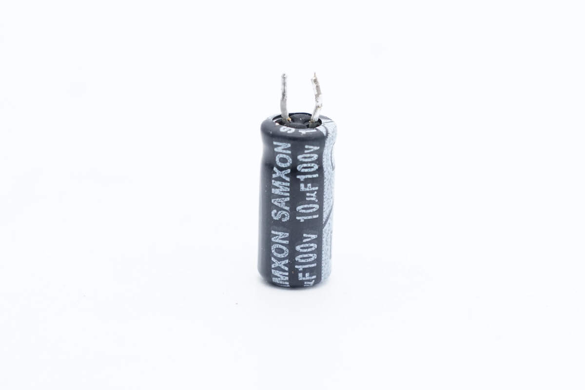
The capacitor that powers the master control chip is from SAMXON. 10μF 100V.
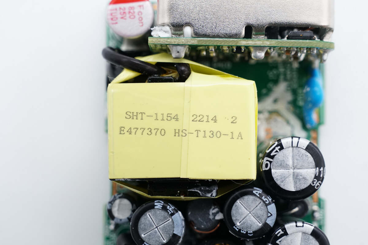
Here is the transformer.
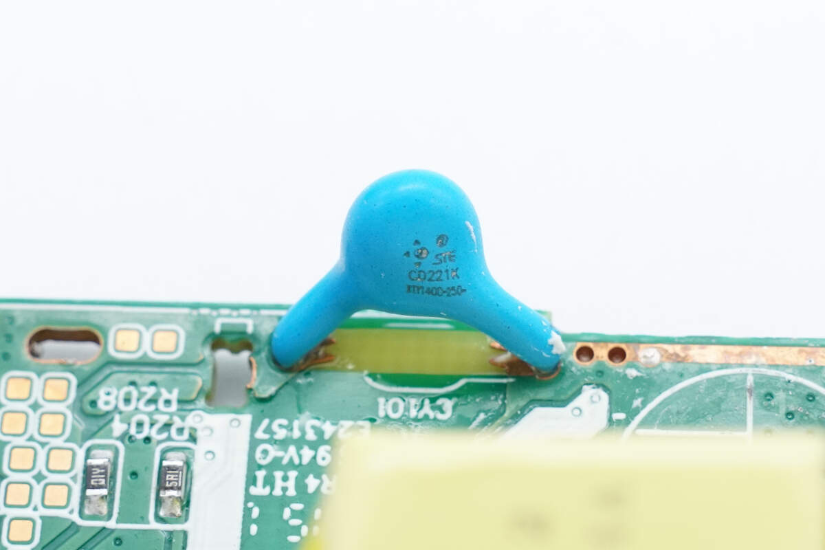
The blue Y capacitor marked with CD221K is from STE.
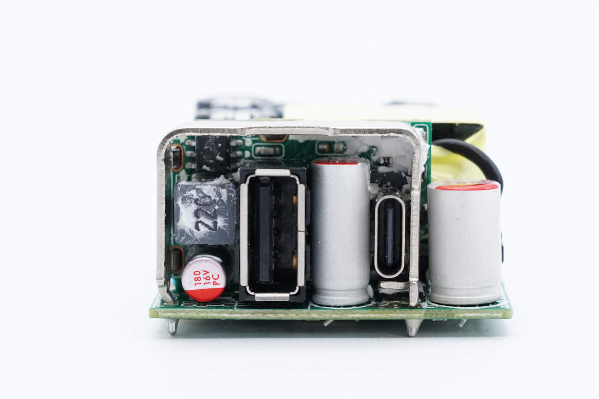
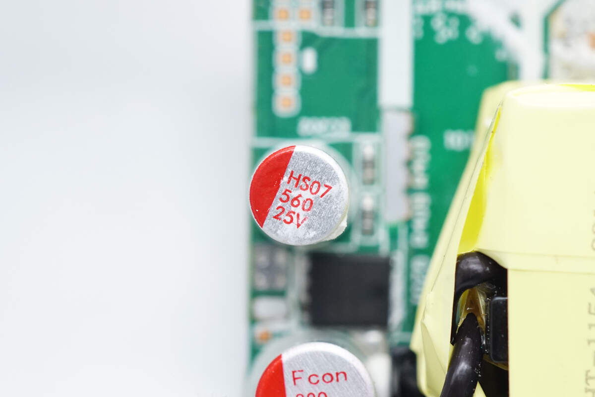
The output end is soldered to a separate small PCB.
Remove the small PCB and you can see a synchronous rectifier between the two solid capacitors.
The synchronous rectifier is from Vergiga and adopts the PDFN5060X package. The withstand voltage is 100V and the resistance is 3.8mΩ. Model is VSP004N10MS-G.
Here is the information about Vergiga VSP004N10MS-G.
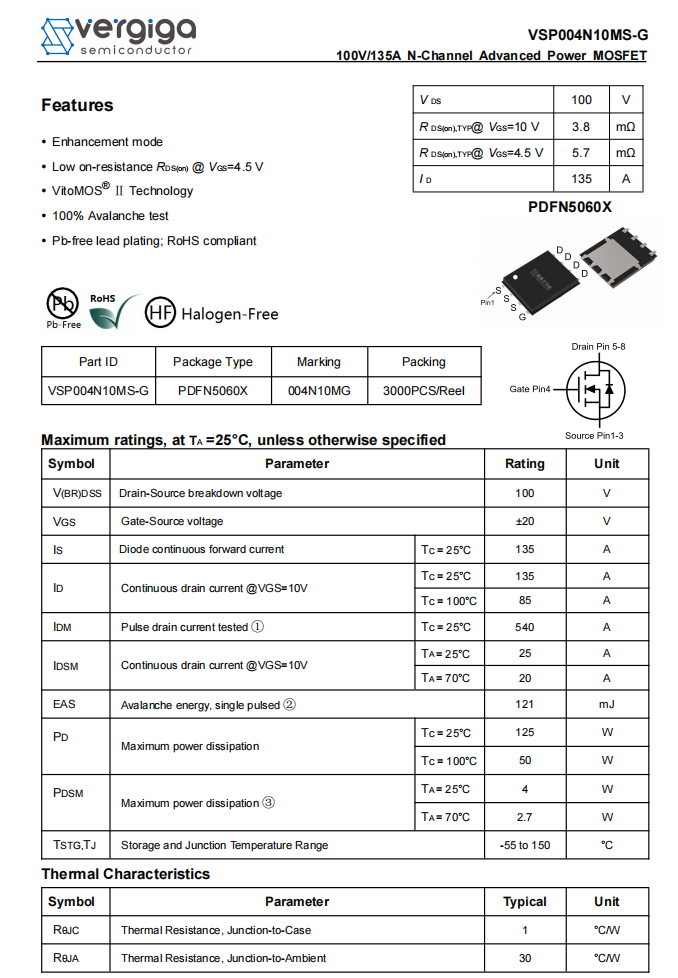
Here is the solid capacitor for output filtering. 820μF 25V.
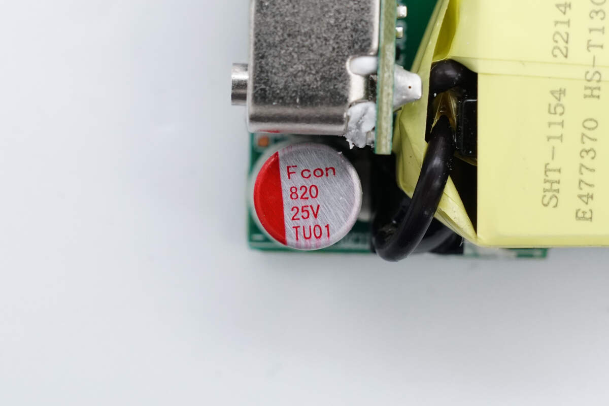
Here is another solid capacitor. 560μF 25V.
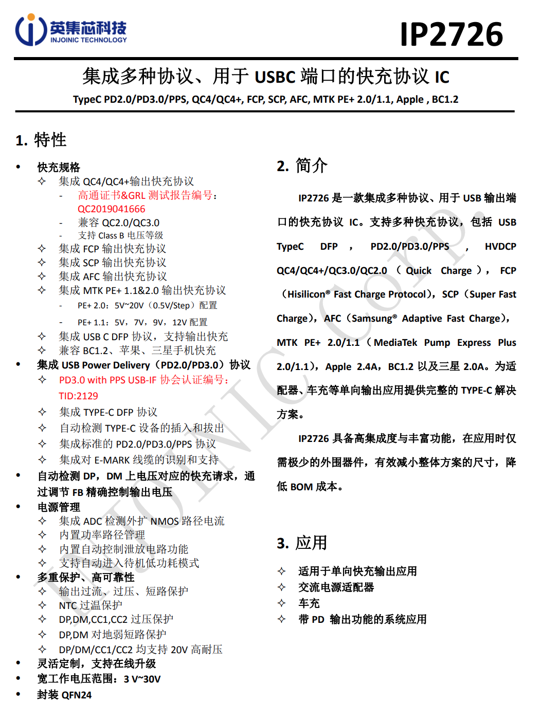
The front of the small PCB at the output end has components such as protocol chip, synchronous buck converter, buck inductor, solid capacitor for output filtering, and VBUS MOSFET.
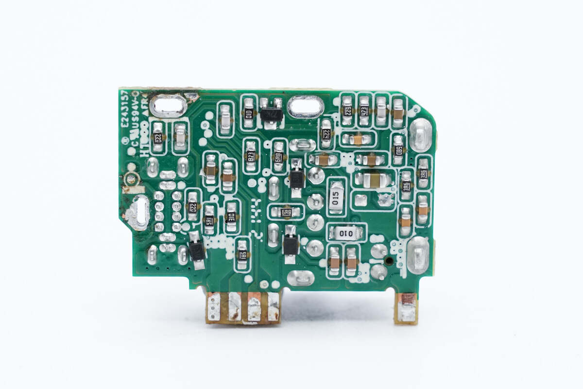
There are small devices such as capacitors and resistors on the back.
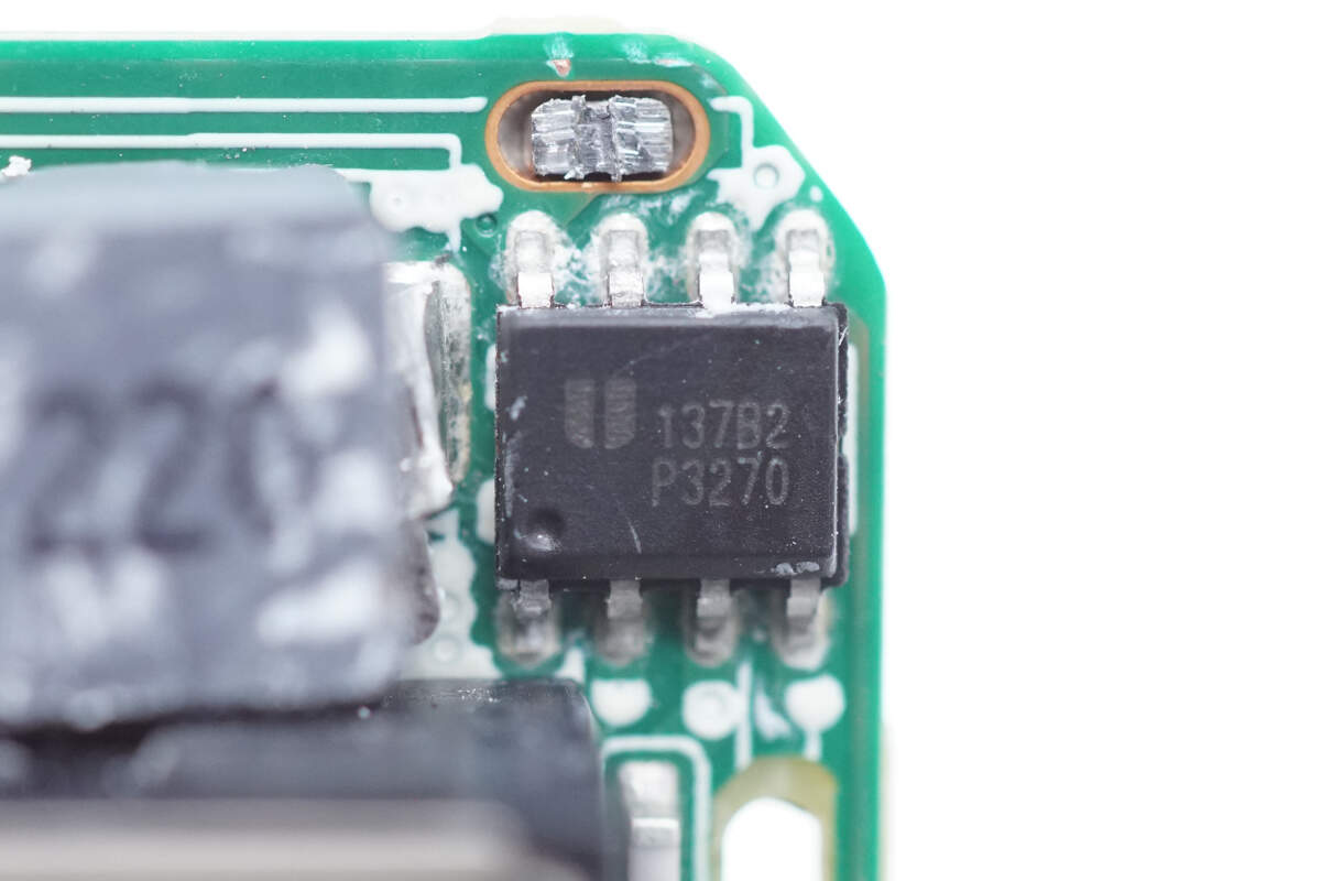
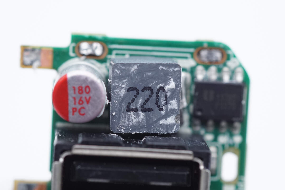
The synchronous buck converter is from Eutech and adopts the SOP-8 (EP) package. It supports an input voltage range of 4.5V-30V, supports pass-through mode, has a built-in MOSFET on the chip, and supports a maximum output current of 4A. Model is EUP3270.
Here is the buck inductor.
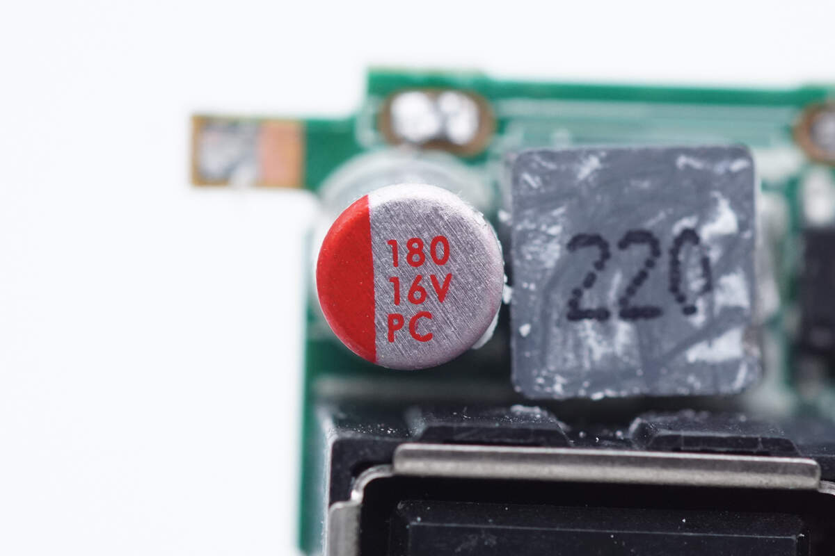
The solid capacitor is used for secondary buck output filtering of the USB-A port. 180μF 16V.
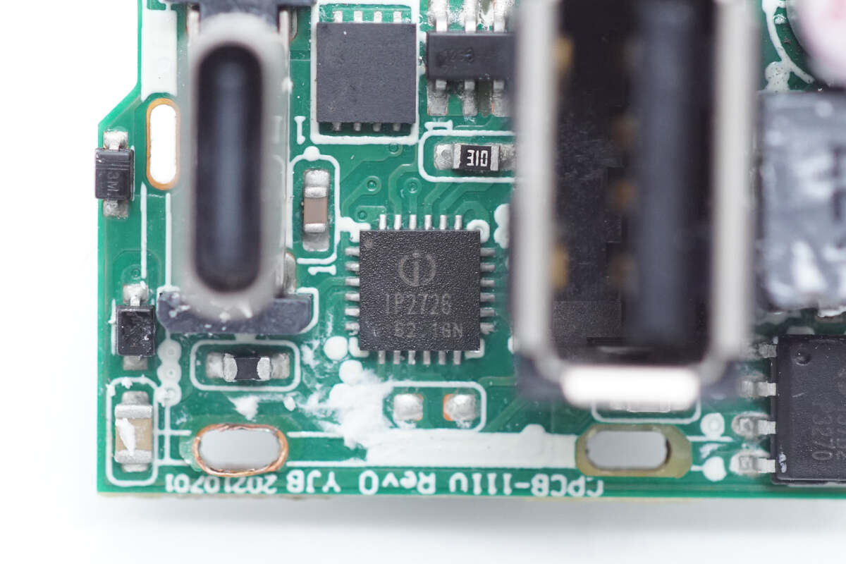
The protocol chip is from INJOINIC. It integrates multiple protocols and supports Type-C DFP, PD2.0/3.0, PPS, QC4+, QC2.0/3.0, FCP, AFC, SCP, MTK PE+, Apple2.4A, BC1.2 and Samsung 2A. With high integration and rich functions, it can effectively reduce the size of the overall solution and reduce BOM cost. Model is IP2726.
Here is the information about INJOINIC IP2726.
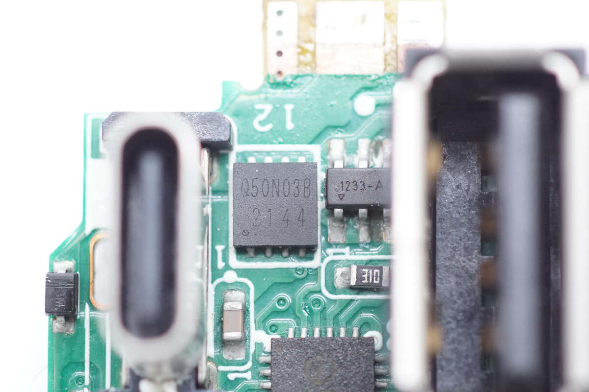
The USB-C output VBUS MOSFET is marked with 050N03B.
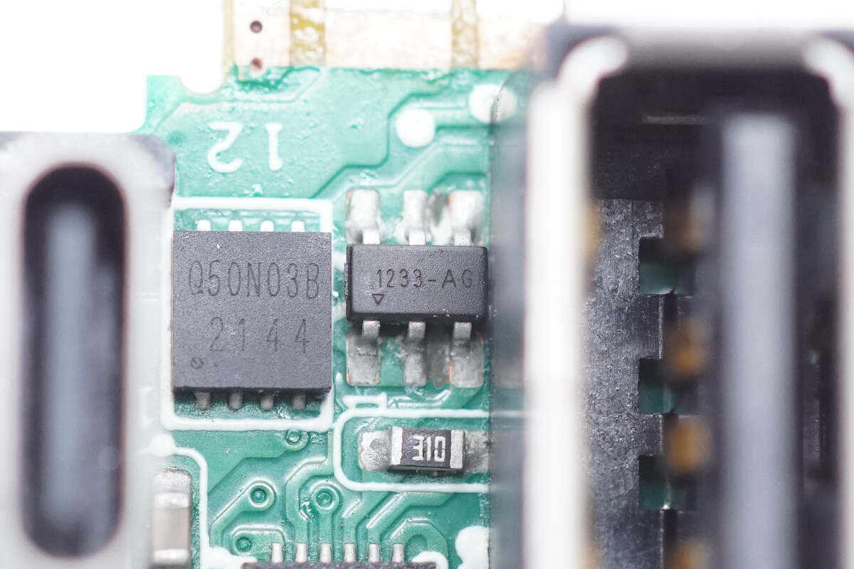
The USB-A output VBUS MOSFET is marked with 1233-AG.

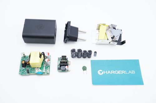
Well, those are all components of the Motorola 50W charger.
Summary of ChargerLAB
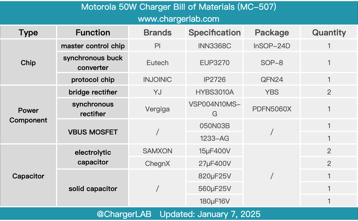
Here is the component list of the Motorola 50W charger for your convenience.
The Motorola 50W charger has a simple design, with the brand logo and the number 50 on the front and back. It is equipped with USB-A and UAB-C output ports and is compatible with the two universal fast charging protocols, QC3.0 and PD3.0. The USB-C port also supports PPS, with maximum output power of 20W and 50W, respectively, meeting the charging needs of two devices at the same time.
After taking it apart, we found it adopts a PI master control chip and Vergiga synchronous rectifier. It adopts the INJOINIC protocol chip used to control the output of the two ports. The PCBA module has been adequately heat-dissipated and insulated and is well-made.
Related Articles:
1. Teardown of ANKER 150W 4 Ports GaN Charger (A2655)
2. Teardown of Xiaomi 30W Magnetic Wireless Charger (MDY-17-EY)
3. Teardown of HP 96W USB-C GaN Charger (ADP-96AW A)