Introduction
More than a year ago, ChargerLAB published a teardown video of Realme 50W mini superdart charger, which adopts a ultra-thin design. You can click the related article at the bottom to check that. And today, we've received a similar product launched by lenovo - the Lenovo 65W Mini GaN Charger. So let's go ahead and take it apart to see its internal comonents and structure.
Product Appearance
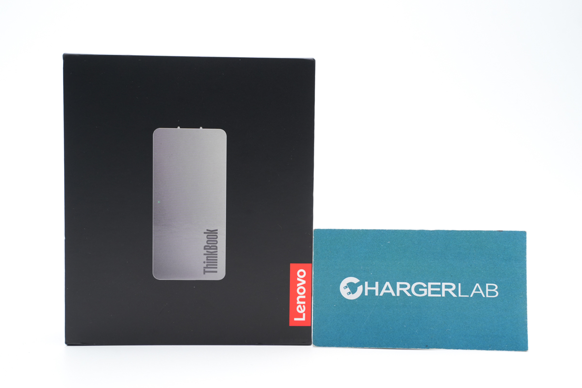
The product appearance and Lenovo are printed on the front of the box.
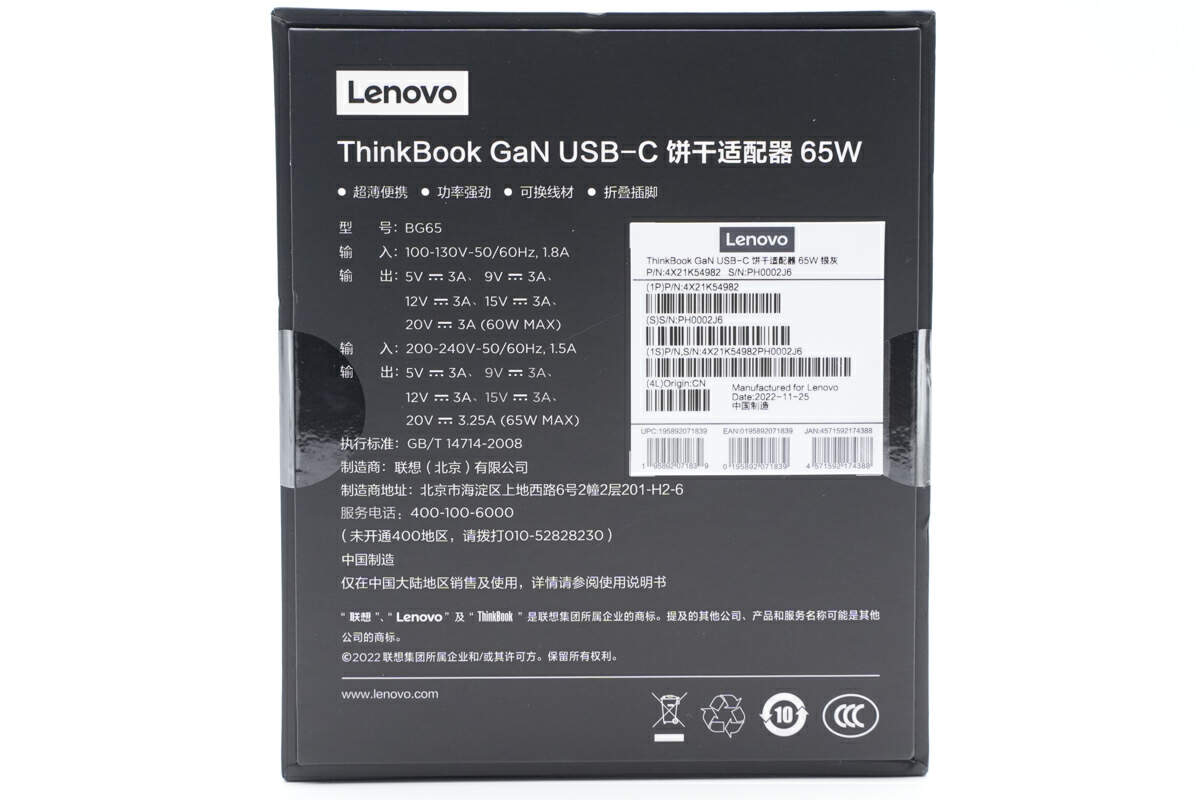
The four major selling points of the product and some specs info are printed on the back.
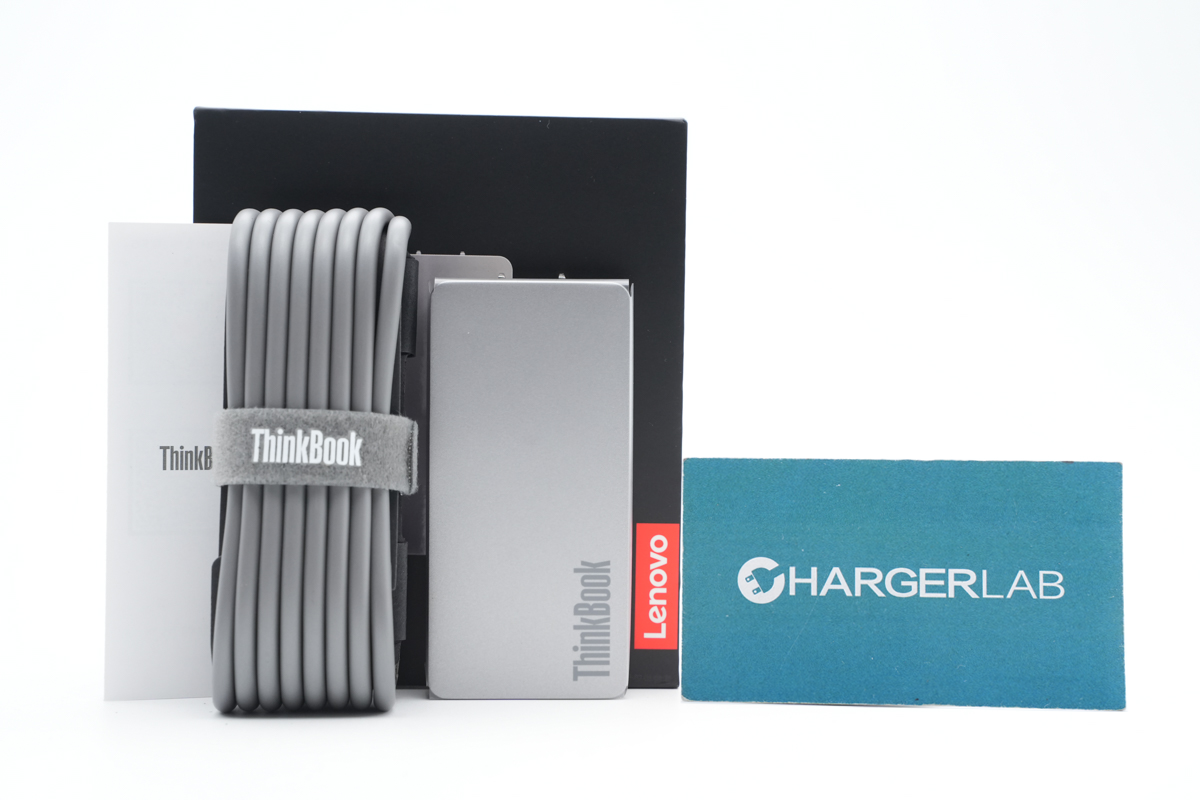
It contains a manual, a cable and the charger itself.
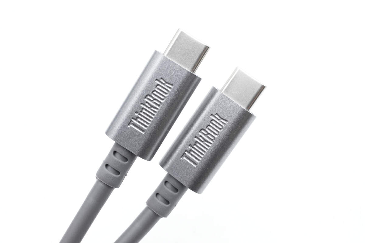
The cable adopts the same silver-grey design as the charger, maintaining a consistent overall tone. The USB-C connector has the word "ThinkBook" on it.
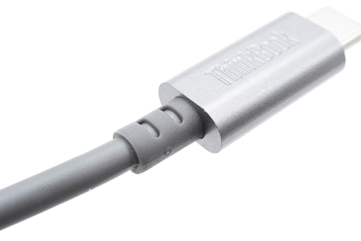
Furthermore, the joint has been reinforced.
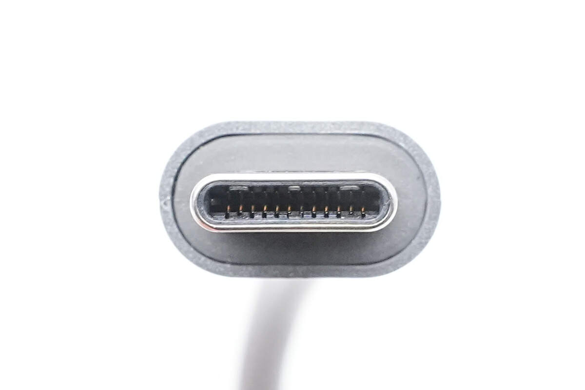
The USB-C male plug adopts a full PIN design.
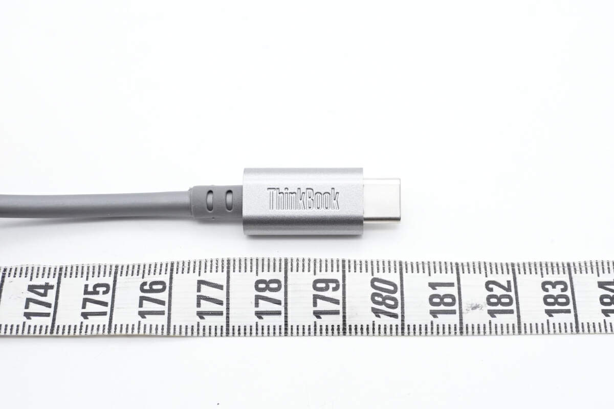
The length of the cable is about 1.8m (5’ 10.92”).
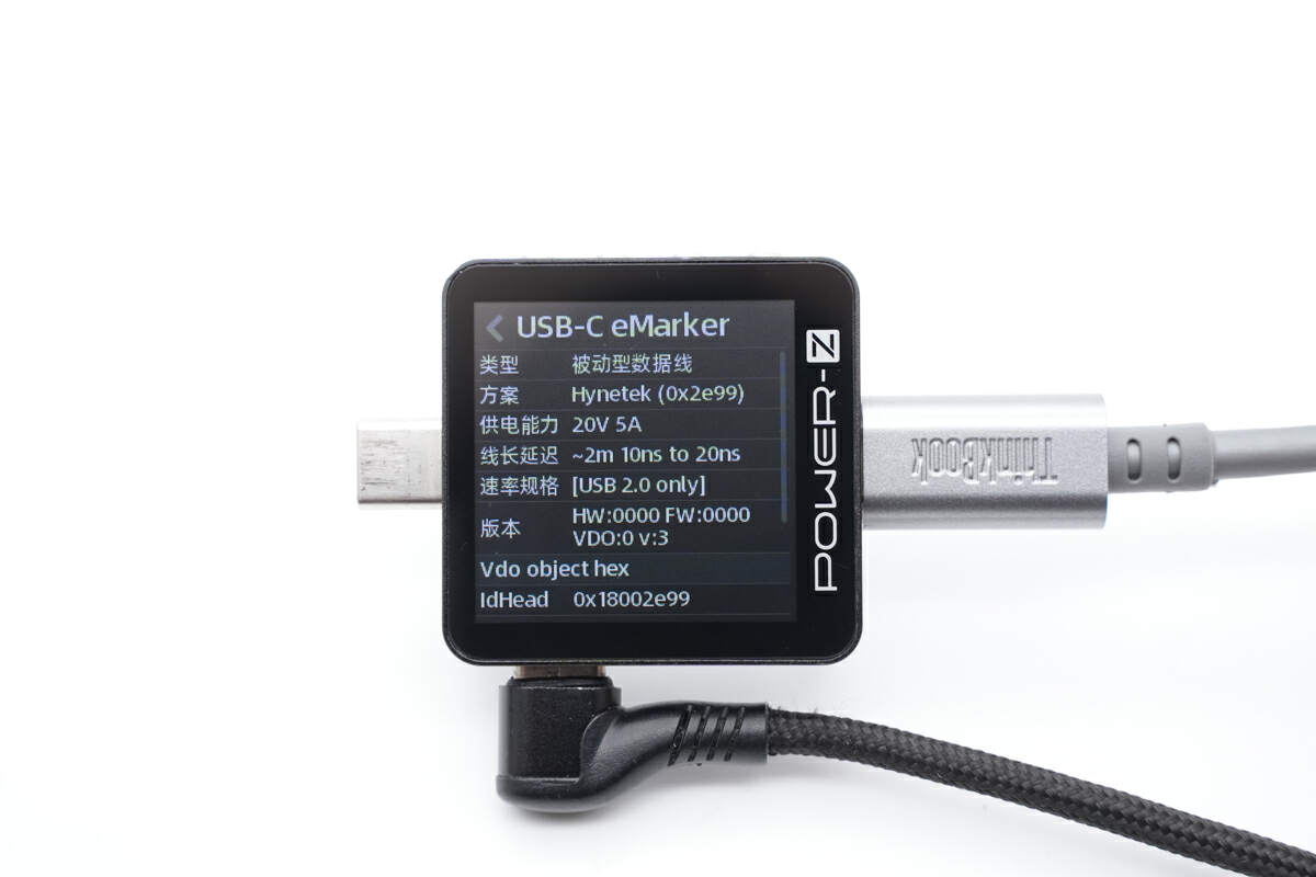
Our ChargerLAB POWER-Z KM003C shows it can support 20V5A PD, and the data transmission speed is limited to USB 2.0.
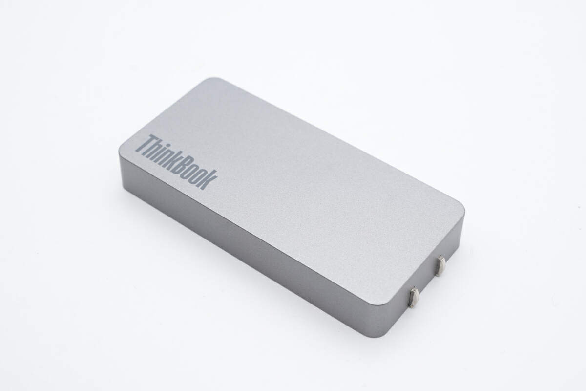
The charger features an ultra-thin design, with an overall silver-grey tone and fine texture matte treatment on the surface, with distinct edges and corners.
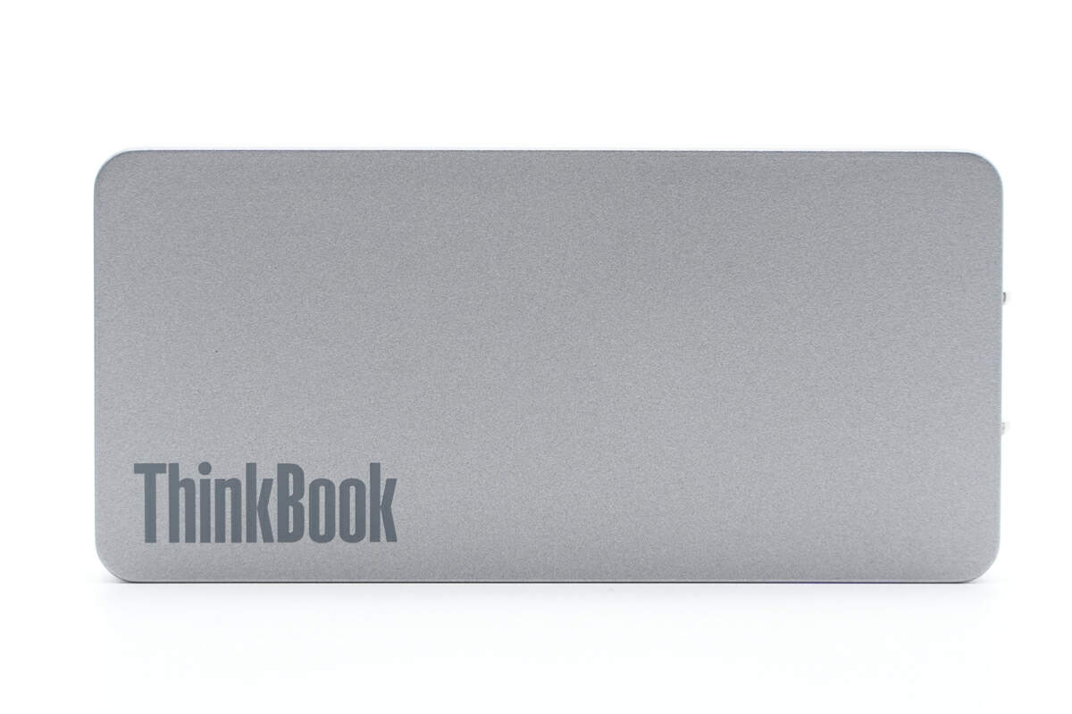
The ThinkBook is marked in the upper corner of the top surface.
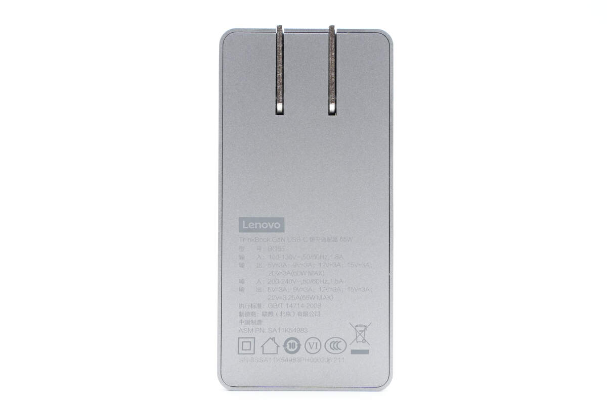
All specs info are printed on the bottom.
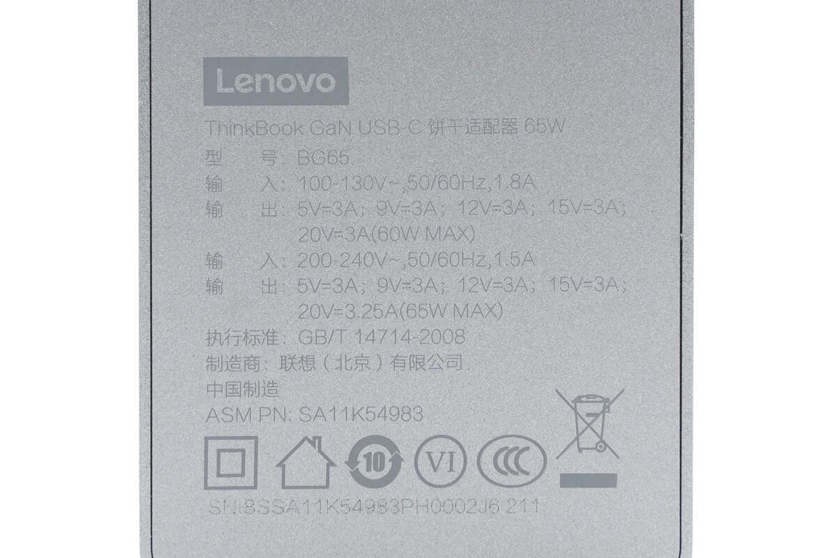
Model is BG65. When the input is 100-130V~50/60Hz 1.8A, the maximum output is 20V3A 60W. When the input is 200-240V~50/60Hz 1.5A, the maximum output is 20V3.25A 65W.
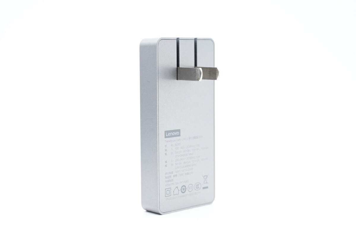
The charger comes with a foldable two-prong plug, which can be hidden inside the charger when not in use, making it easy to carry.
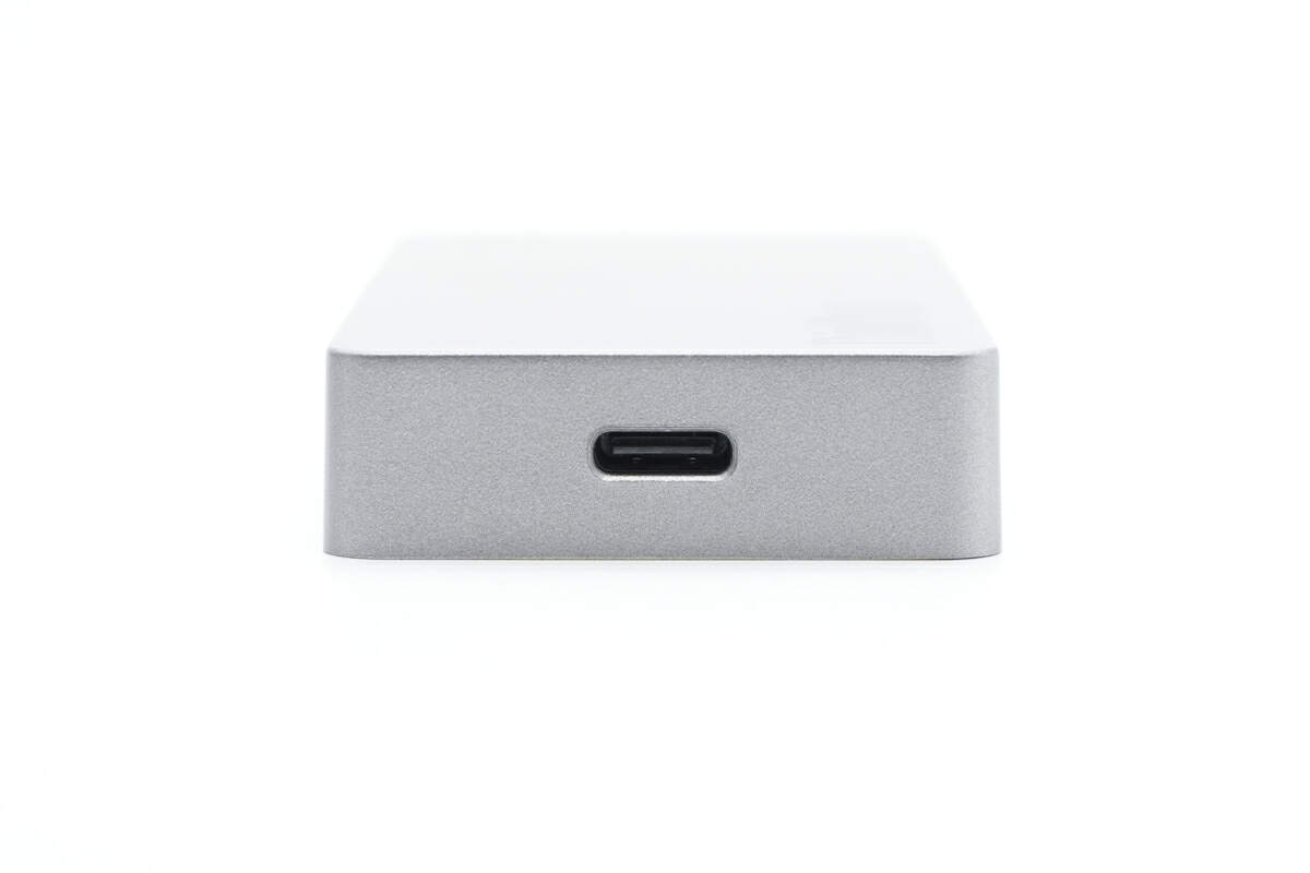
And the plastic sheet inside the USB-C port is black.
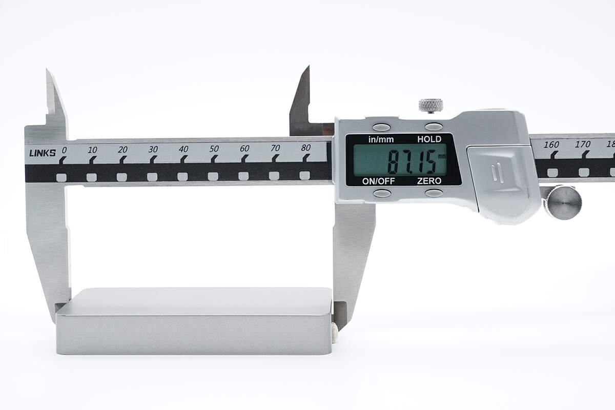
The length of the charger is about 87mm (3.43 inches).
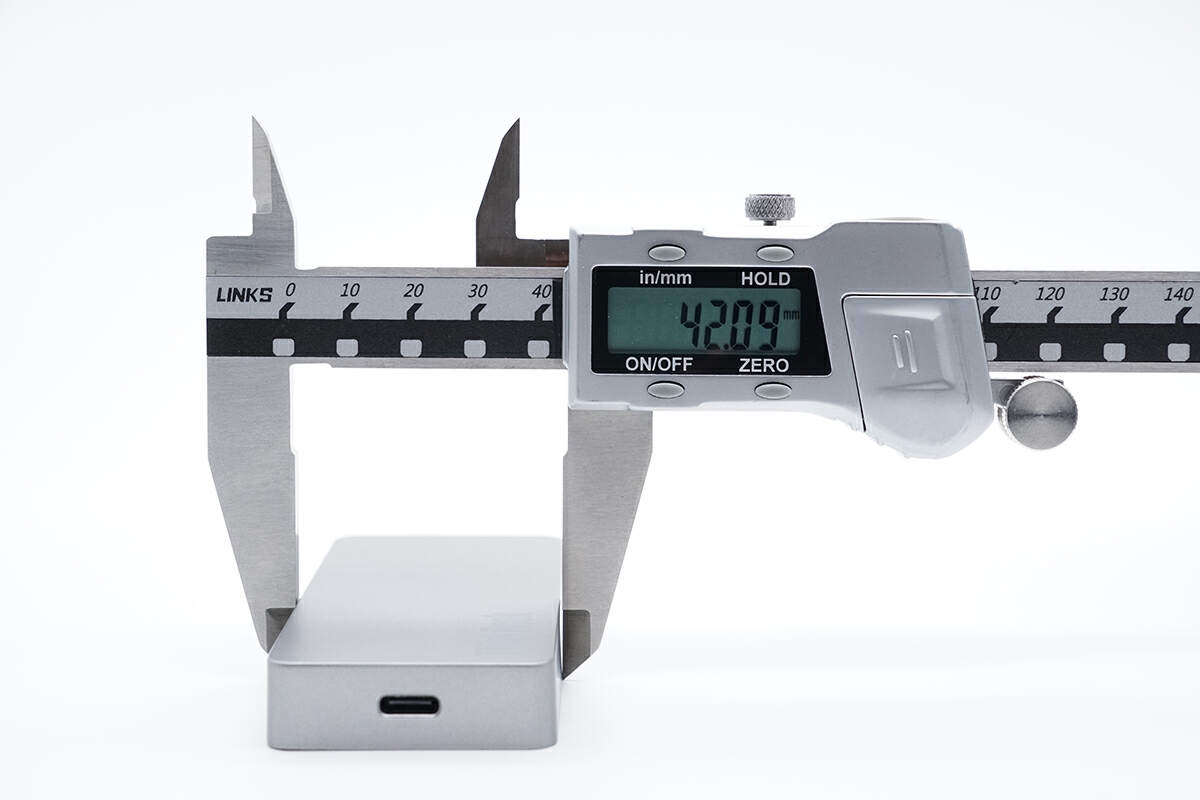
The width is about 42mm (1.65 inches).
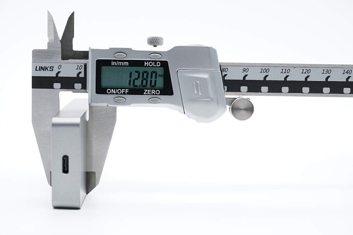
And the height is about 13mm (0.51 inches).
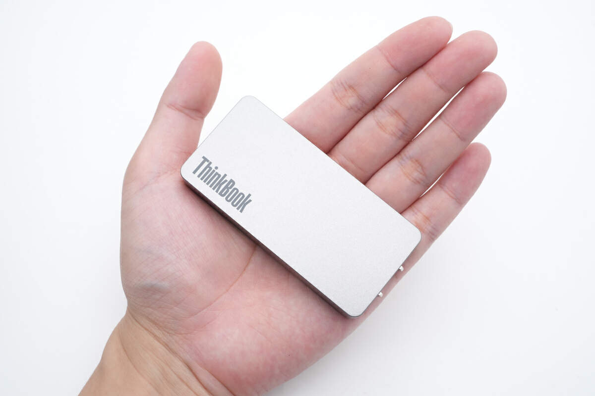
This is how it looks like on my hand.
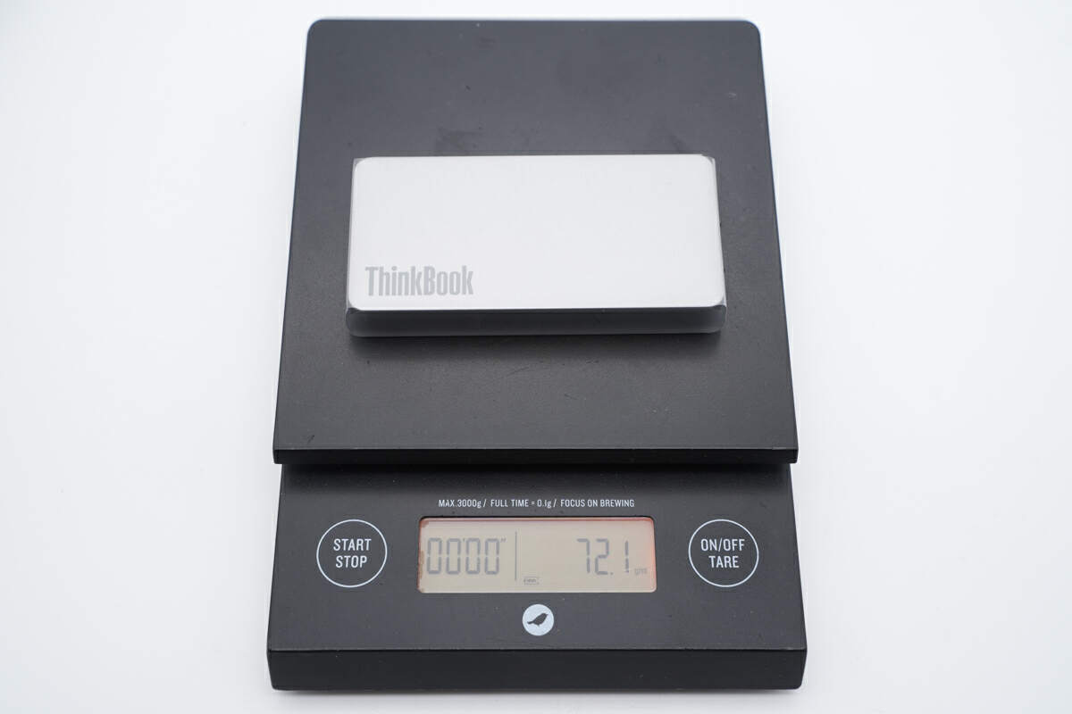
The weight is about 72g (2.54 oz).
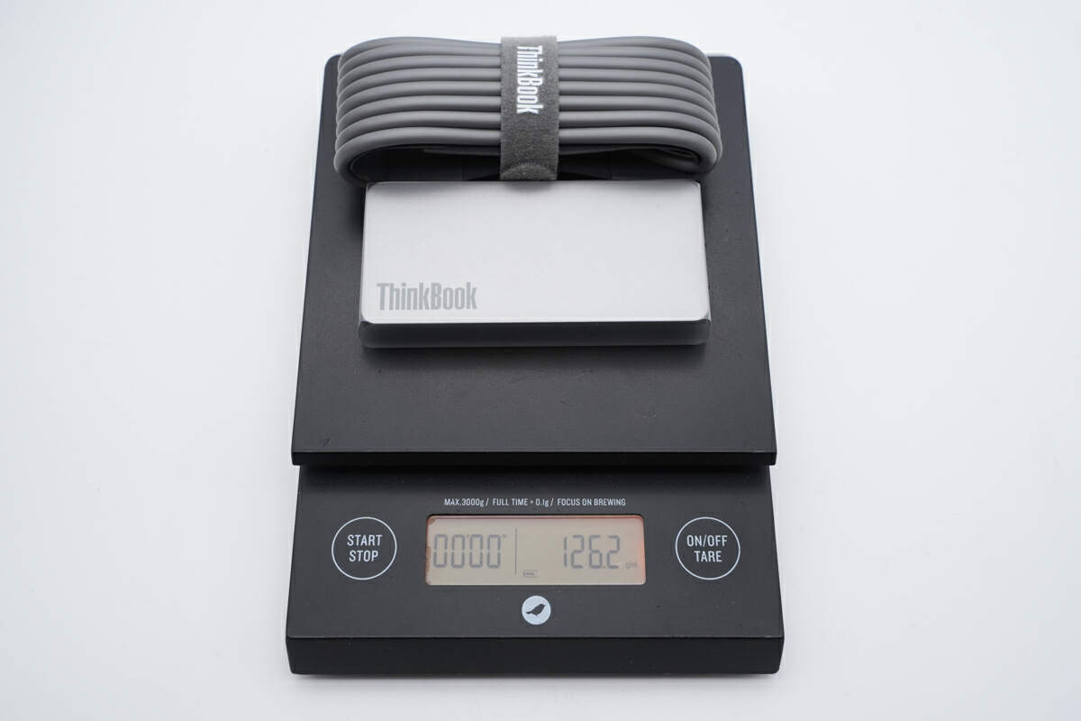
And the total weight is about 126g (4.44 oz).
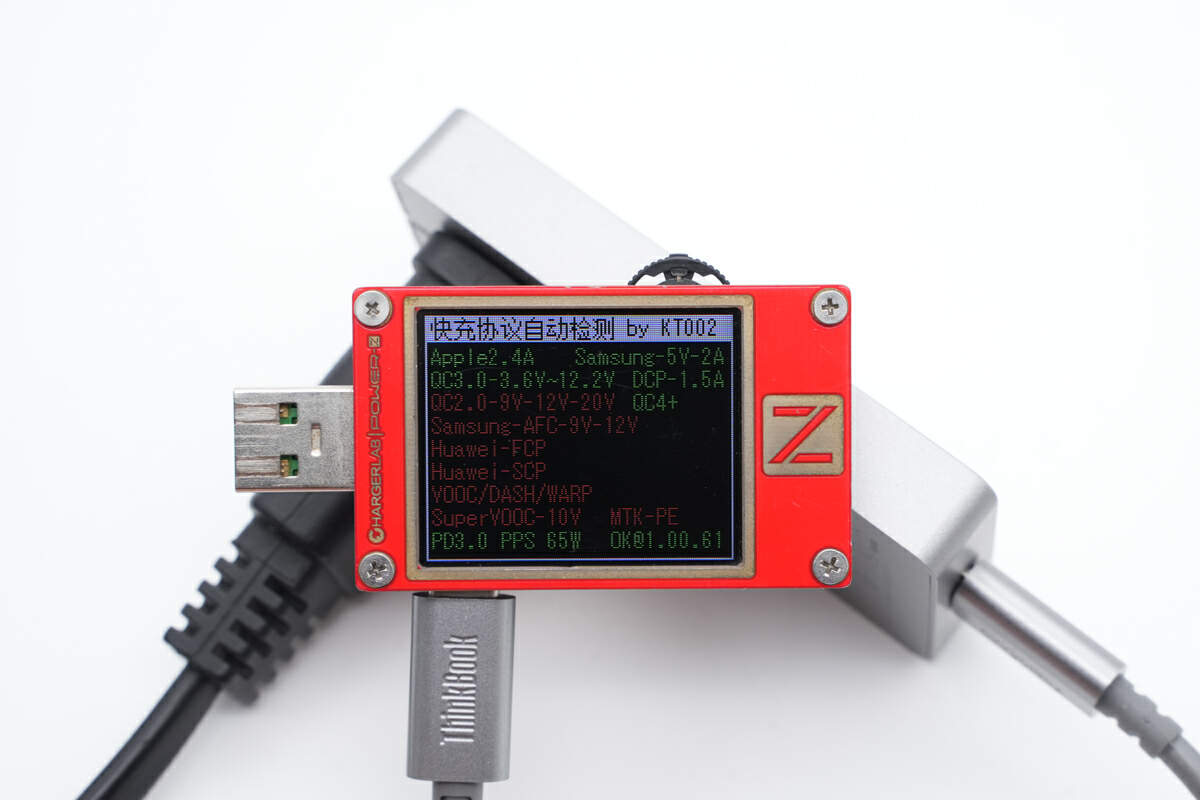
The ChargerLAB POWER-Z KT002 shows the USB-C port supports Apple 2.4A, Samsung 5V2A, DCP, QC3.0, QC4+, PD3.0, and PPS protocols.
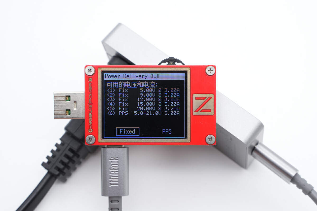
It also supports five fixed PDOs of 5V/9V/12V/15V 3A, 20V 3.25A, and a set of PPS.
Teardown
Next, let’s go ahead and take it apart.
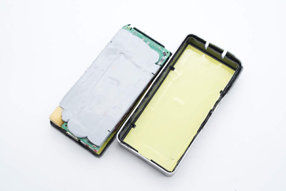
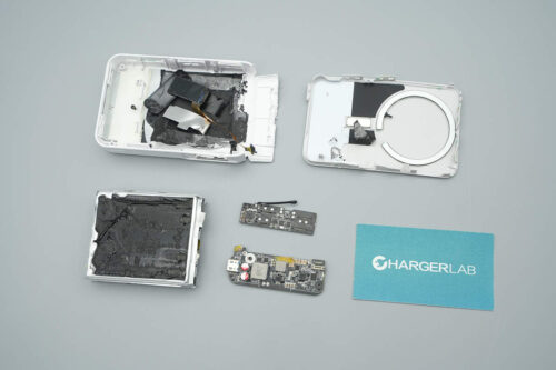
Use a spudger to pry along the gap reveals that the PCB is covered with silicone adhesives for heat dissipation, and insulated with yellow tape.
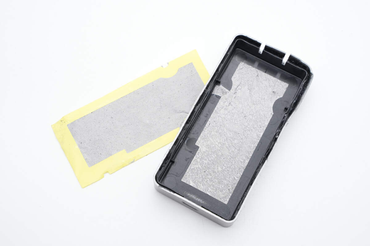
And there is a layer of graphite thermal sheet blow it, which further evenly dissipates heat.
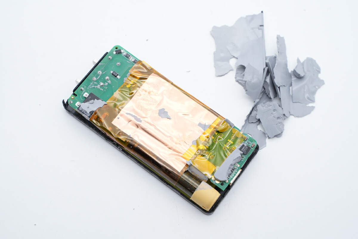
Clean up the adhesives, and the PCBA module has copper foil for shielding.
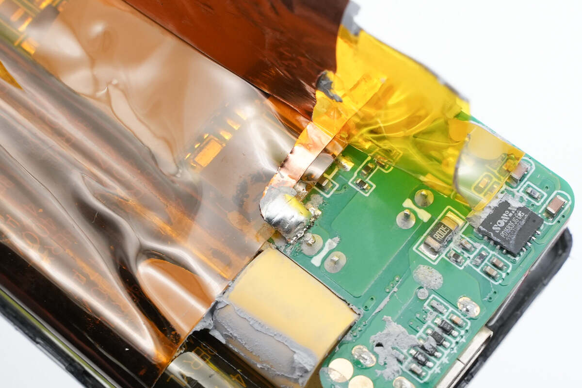
The copper foil is pasted on heat resistant tape for insulation and connected to the PCBA module.
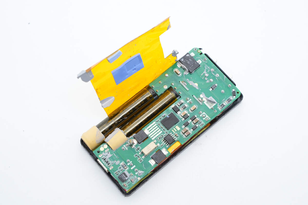
There is another thermal sheet underneath the heat resistant tape.
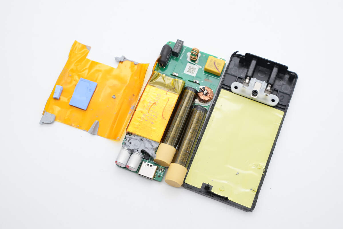
Next, take out the PCBA module.
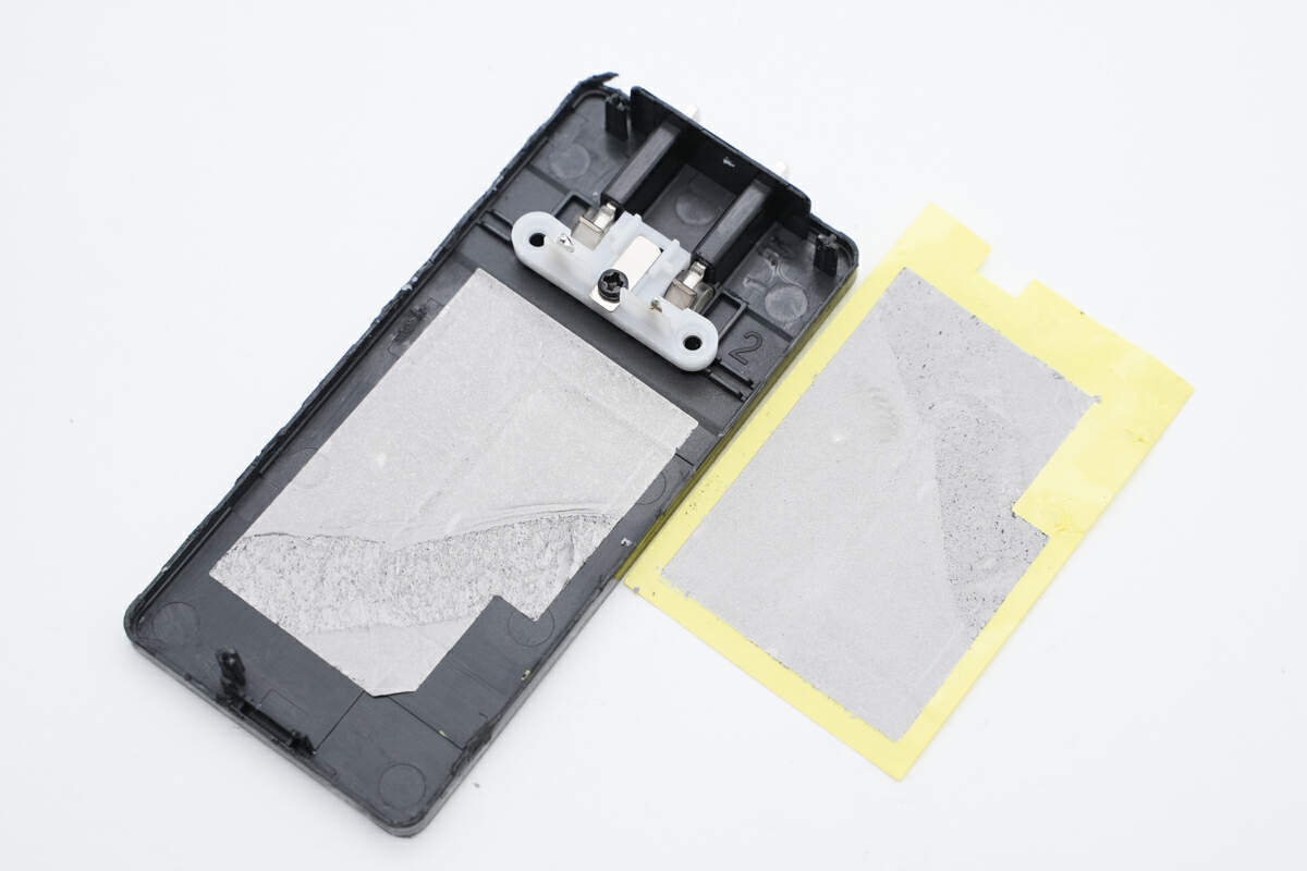
Yellow tape is also pasted inside the other case, and a graphite thermal sheet is under it.
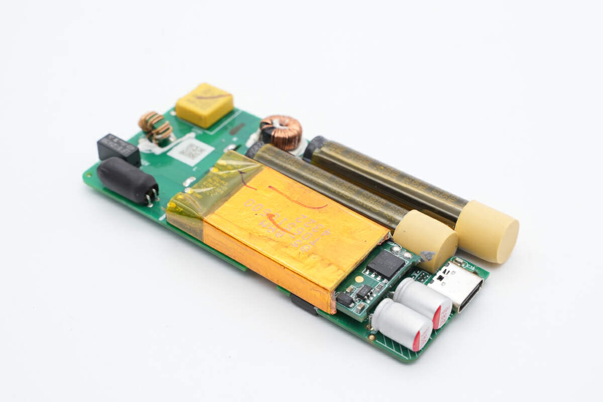
The planar transformer is parallel soldered onto the PCBA module to increase space utilization.
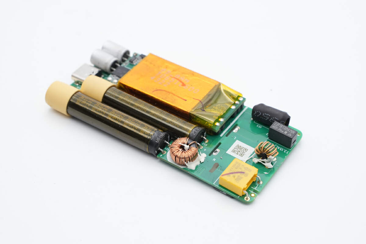
So is the high-voltage filter capacitors.
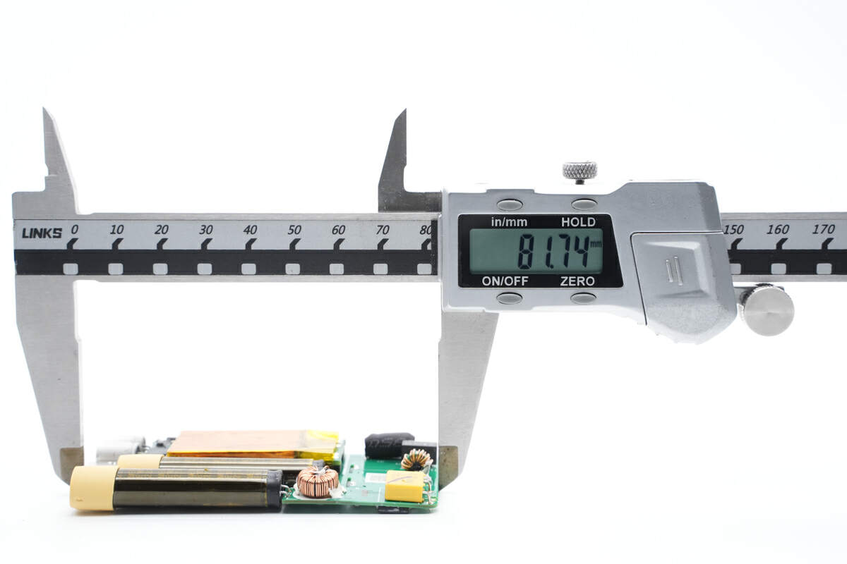
The length of the PCBA is about 82mm (3.23 inches).
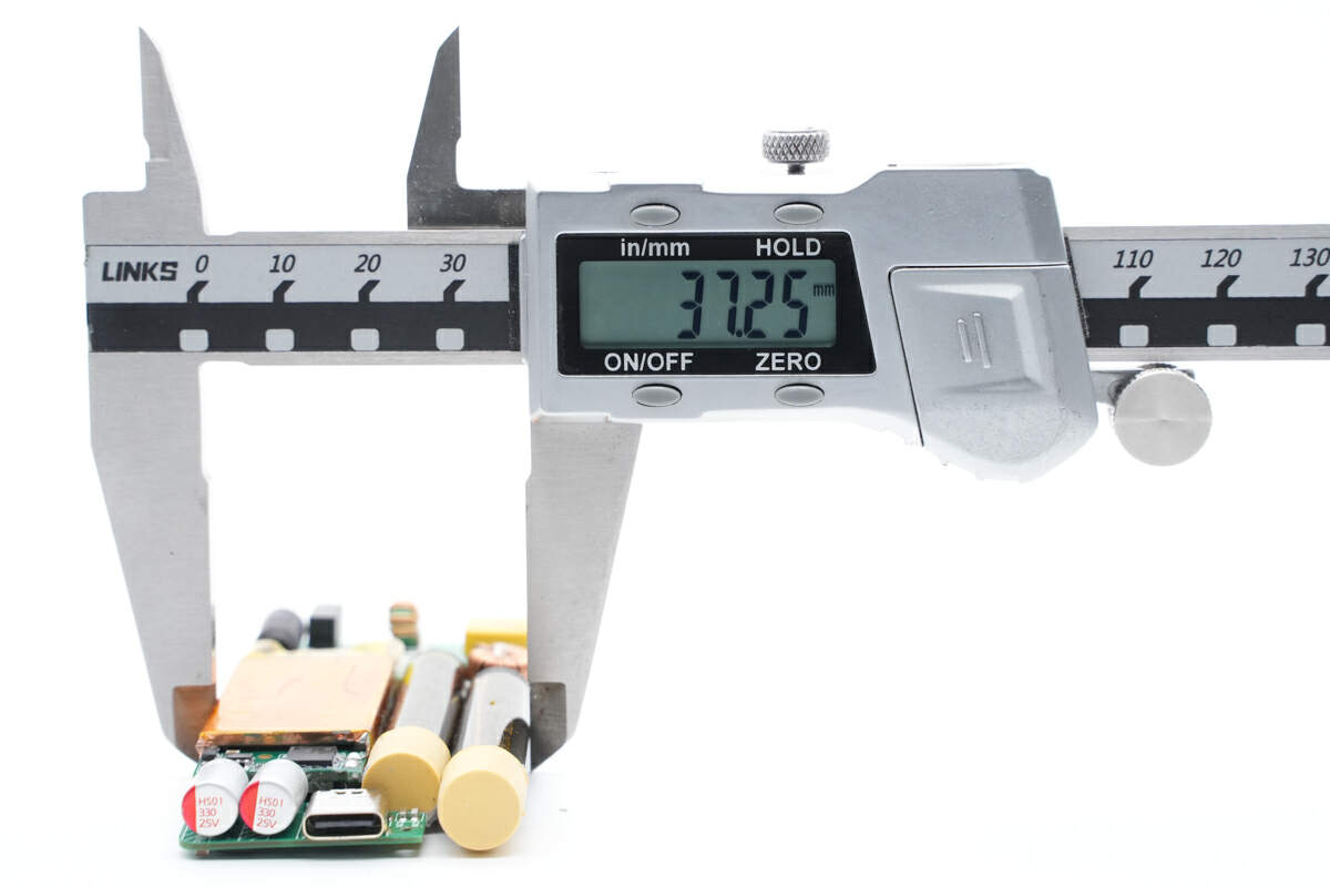
The width is about 37mm (1.46 inches).
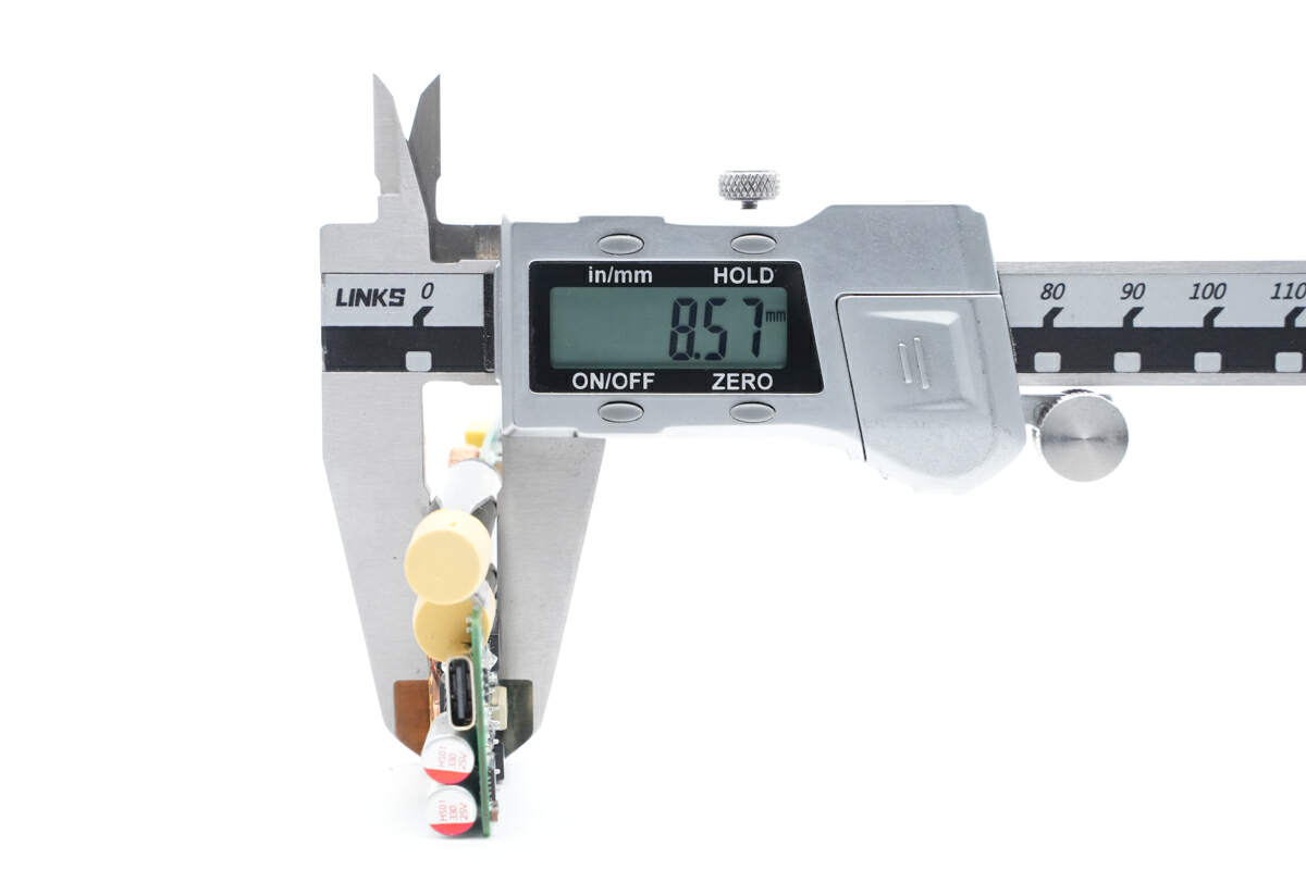
And the height is about 9mm (0.35 inches).
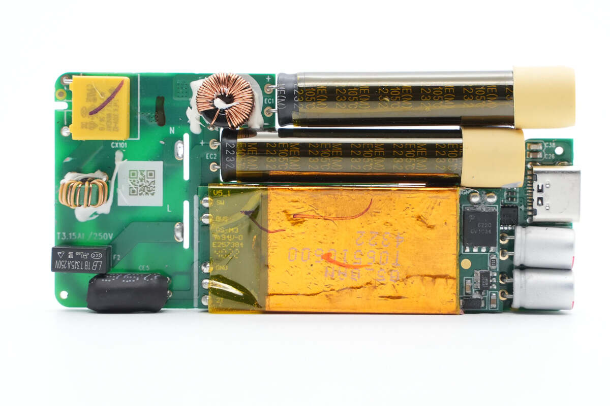
The high-voltage electrolytic capacitors, solid capacitor for output filtering and planar transformer are on the front of the PCBA module.
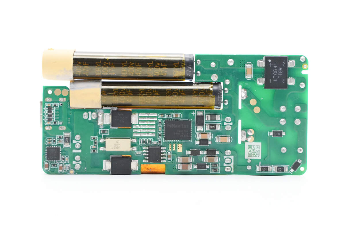
And the bridge rectifier, GaN controller, GaN power chip, SMD Y capacitor and feedback optocoupler are on the back.
ChargerLAB found that this charger adopts a QR flyback topology with a wide output voltage range. The output voltage is controlled by the protocol chip and regulated by optocoupler.
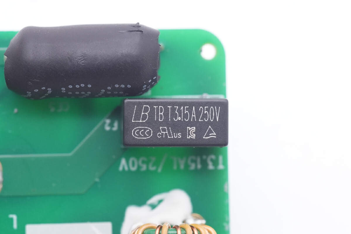
The time-delay fuse is from Lanbaofuse TB series. 3.15A 250V.
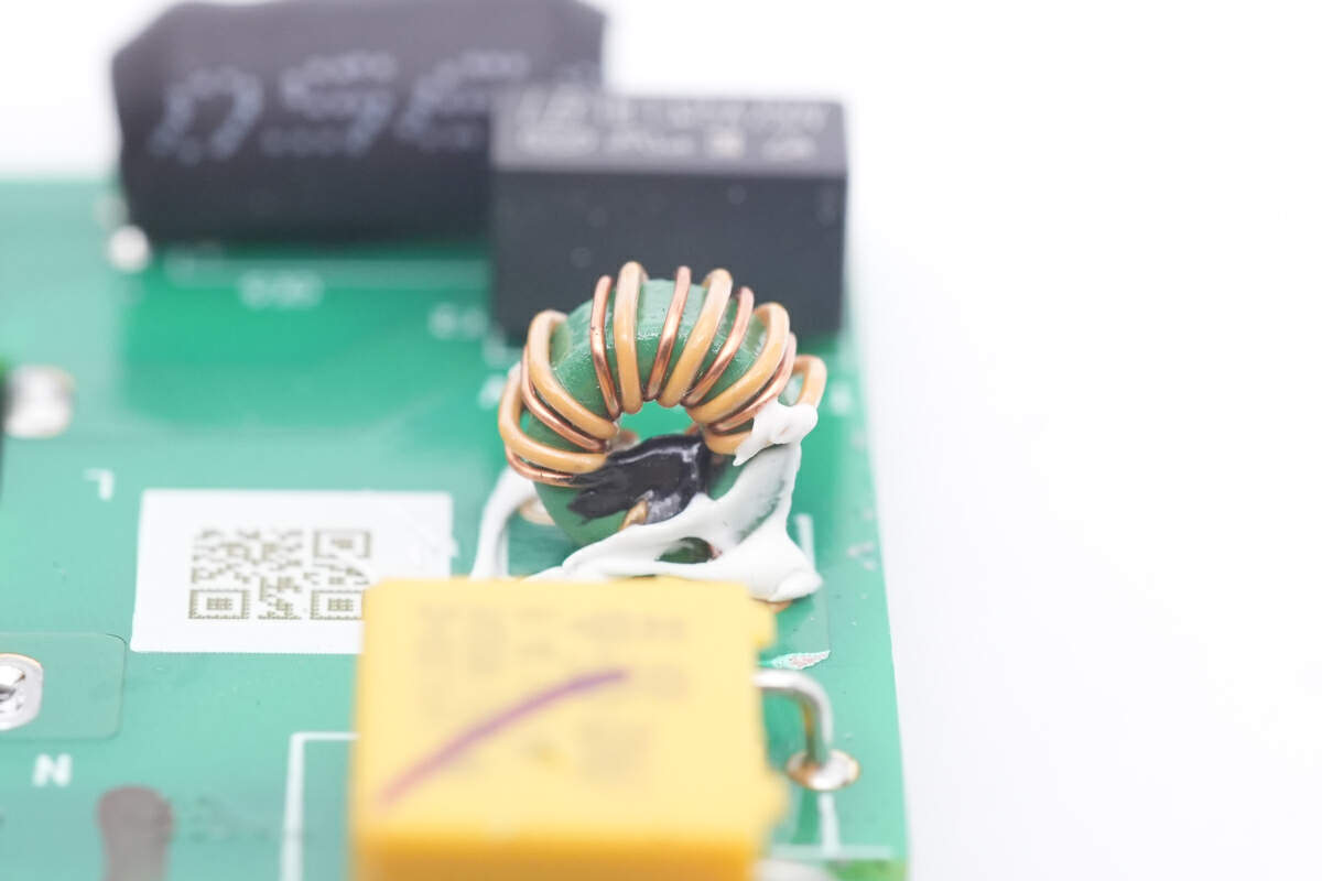
The common mode choke is wound with magnet wires and insulated wires.
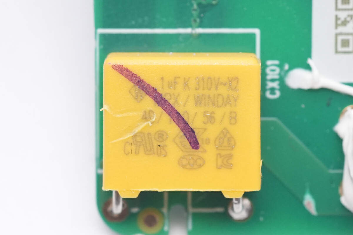
The safety X2 capacitor is 0.1μF.
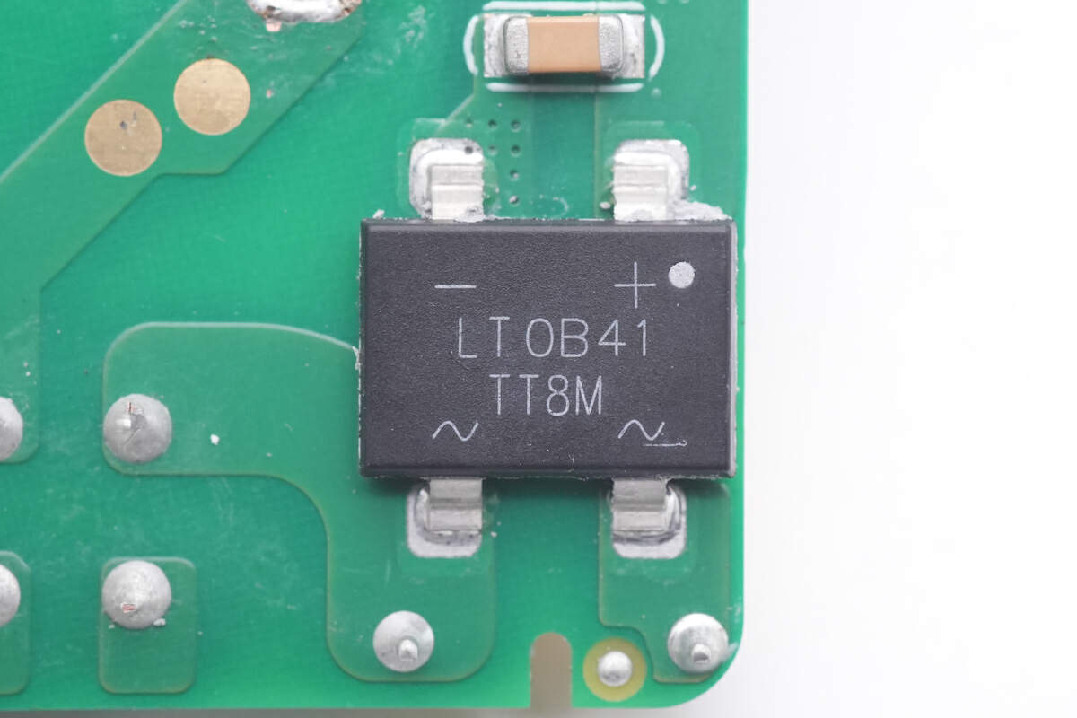
The bridge rectifier's model is TT8M. 8A 1000V.
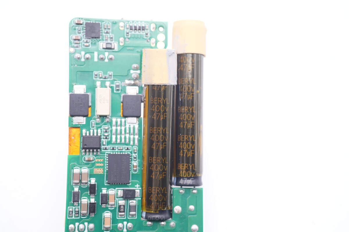
Two high-voltage filter capacitors are from BERYL. 400V 47μF.
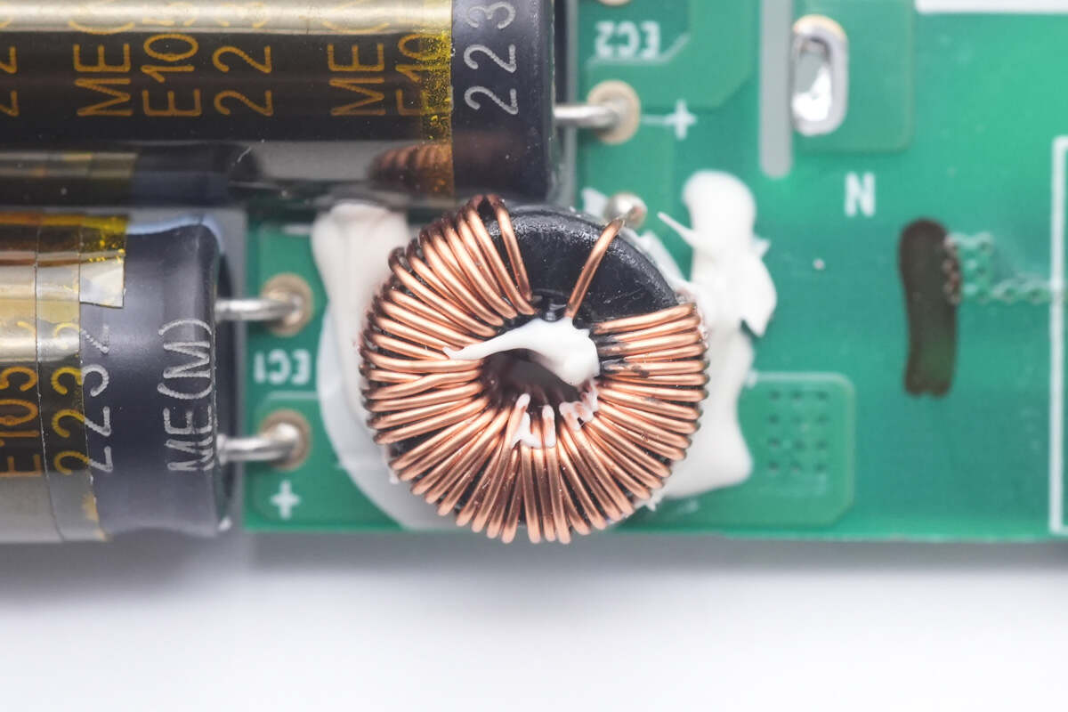
The differential mode choke is wound with magnet wires and fixed by adhesives.
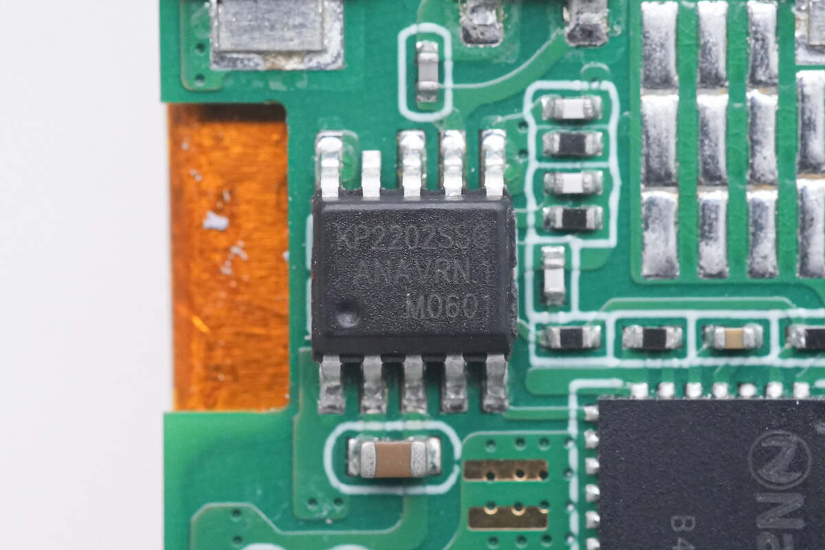
The master control chip is from Kiwi Instruments, model KP2202, which is a high-frequency QR flyback PWM controller. The chip has built-in high-voltage start-up and X-capacitor discharge functions, and has the advantages of fast start-up capability and low standby power consumption. It also supports 500kHz switching frequency, power-saving mode, and standby power consumption is less than 30mW.
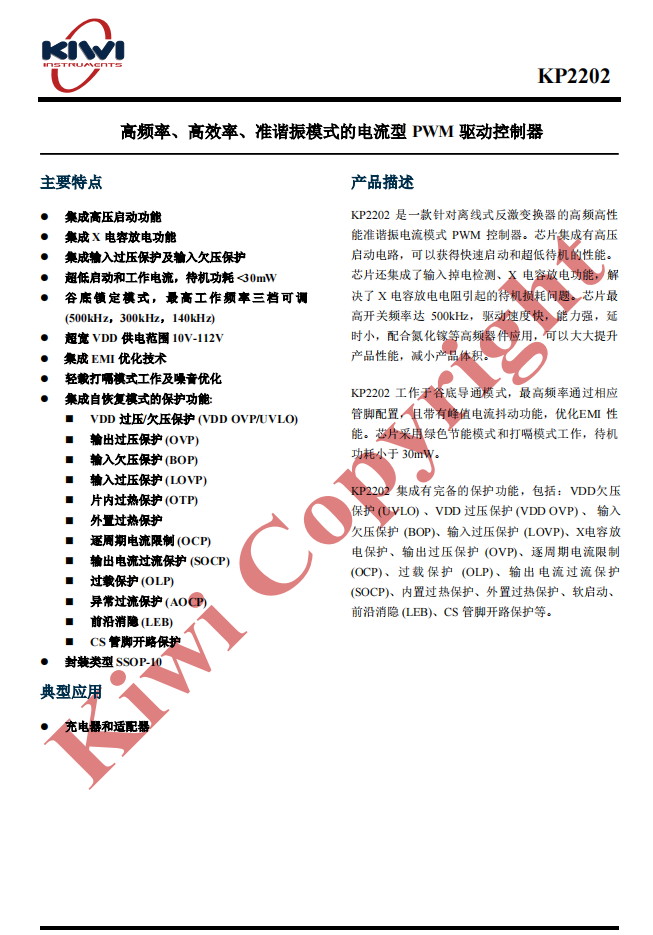
Here is all the information about KP2202.
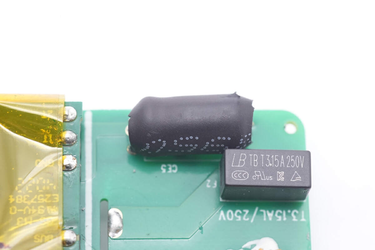
The filter capacitor that powers the master control chip is insulated with a heat-shrinkable tubing.
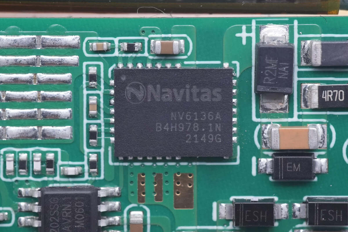
The highly integrated GaN power chip is from Navitas, model NV6136A, which has a built-in driver and a high-precision lossless current sampling circuit to eliminate the loss of the sampling resistor.
It supports a switching frequency of 2MHz and adopts a 6 x 8mm QFN package. 170mΩ 700V.
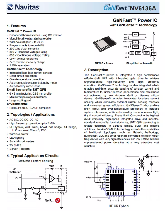
Here is all the information about NV6136A.
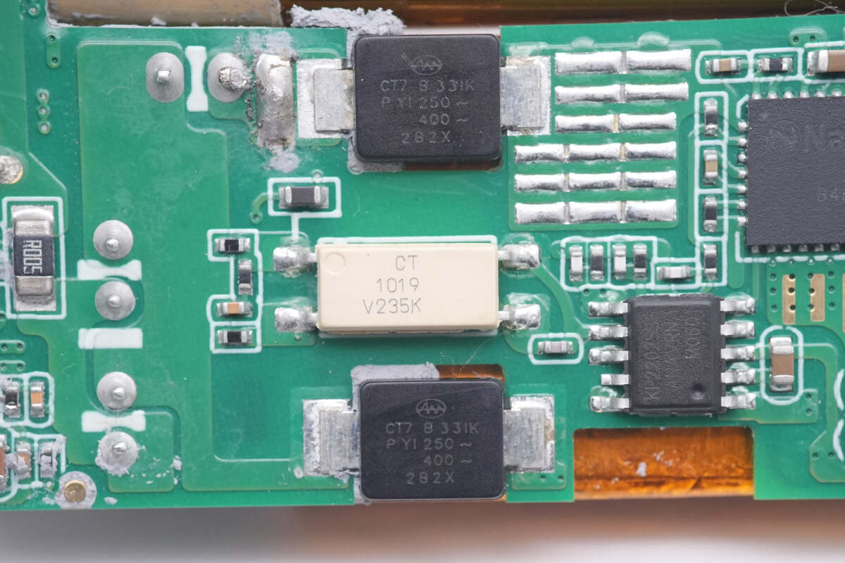
The feedback optocoupler is soldered between the two SMD Y capacitors.
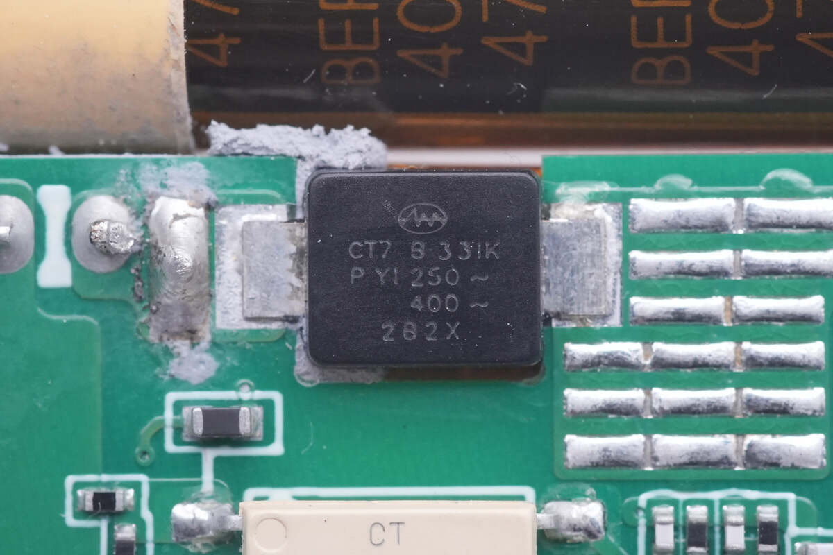
The SMD Y capacitor is from Anshan Keifat. It is a plastic-sealed Y1 capacitor with a specification of 331K.
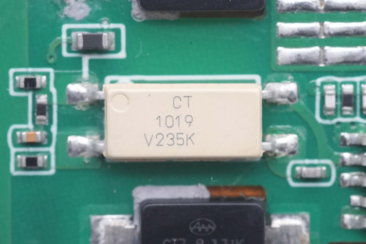
And the CT1019 optocoupler is used for output voltage regulation.
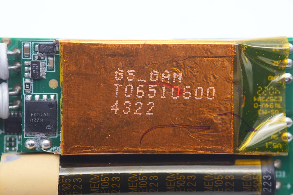
The planar transformer is shielded with copper foil and insulated with heat resistant tape.
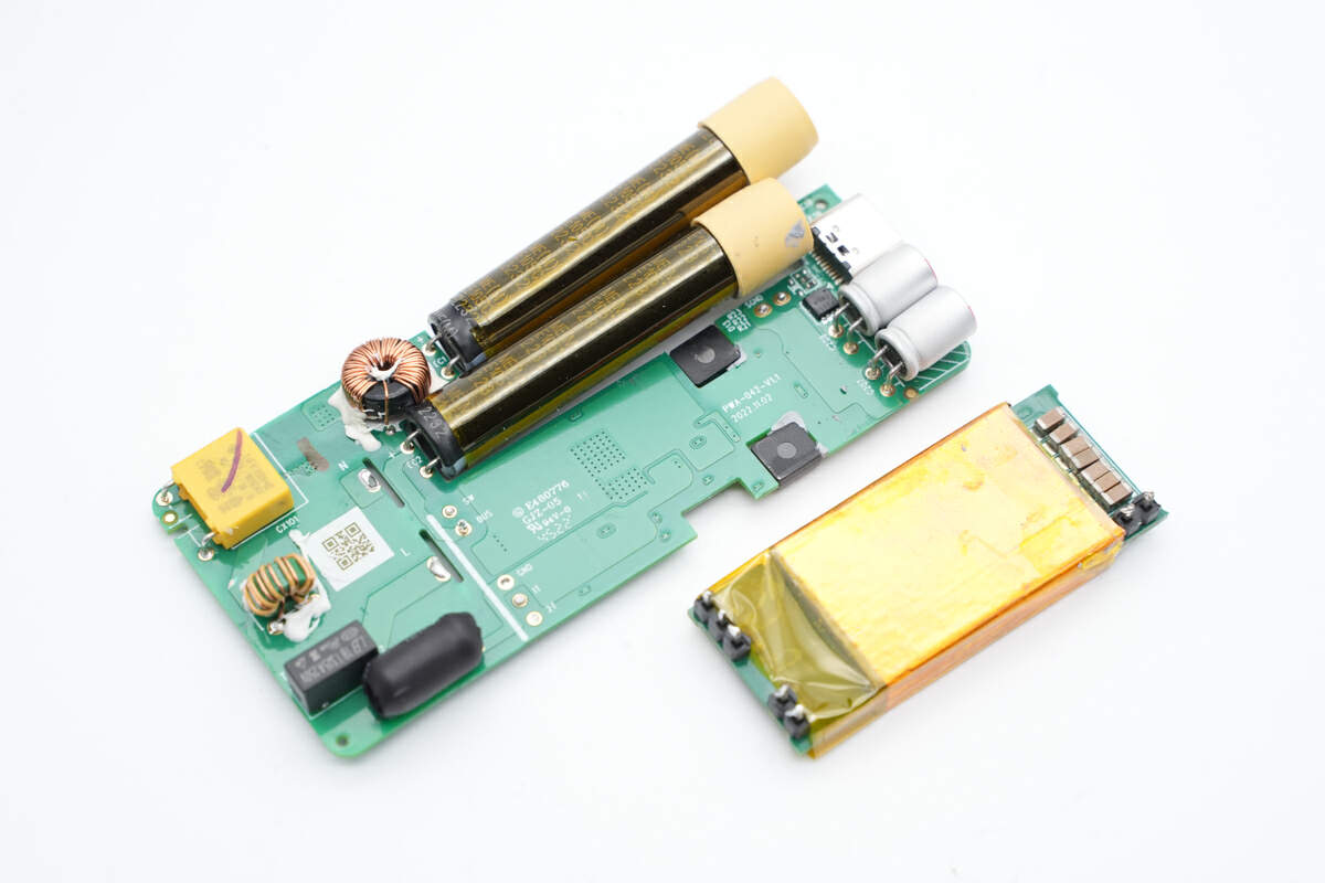
Next, remove the planar transformer.
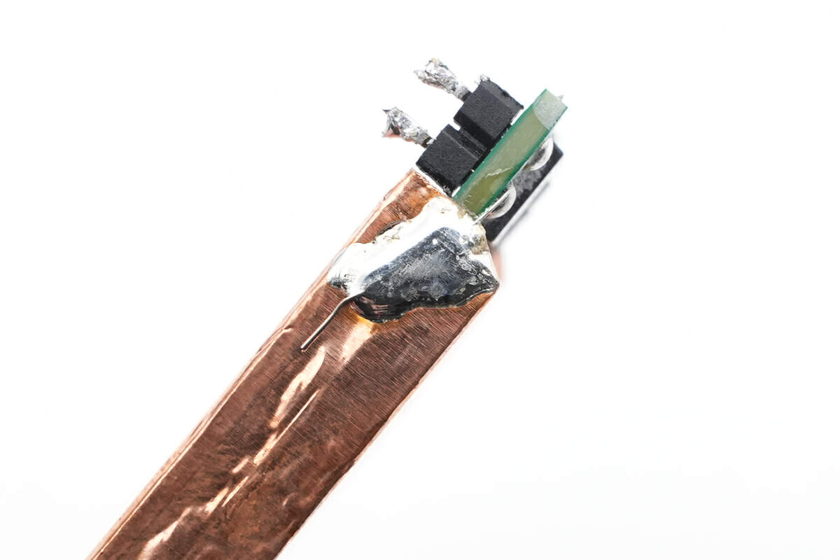
The copper foil is grounded.
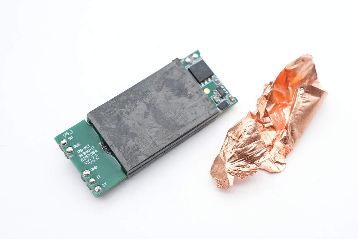
Tear it off.
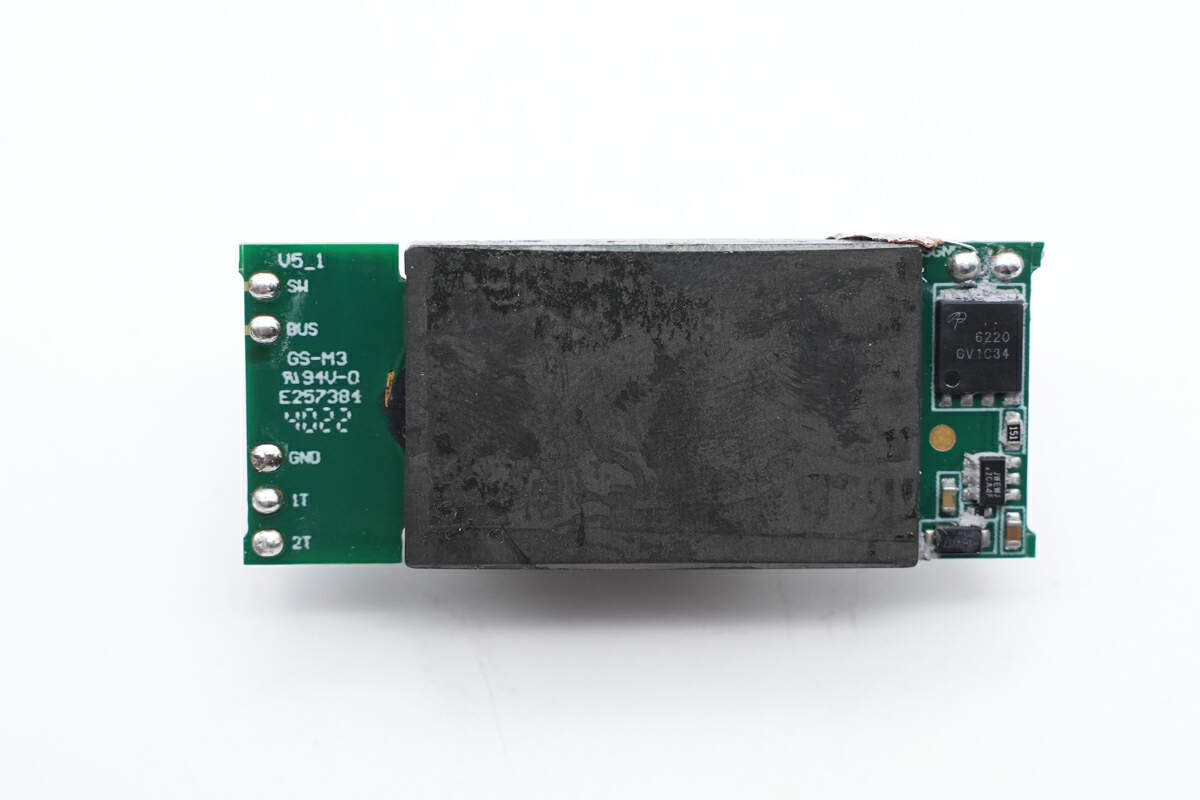
The output end of the planar transformer is soldered with a synchronous rectifier controller and a synchronous rectifier MOSFET.
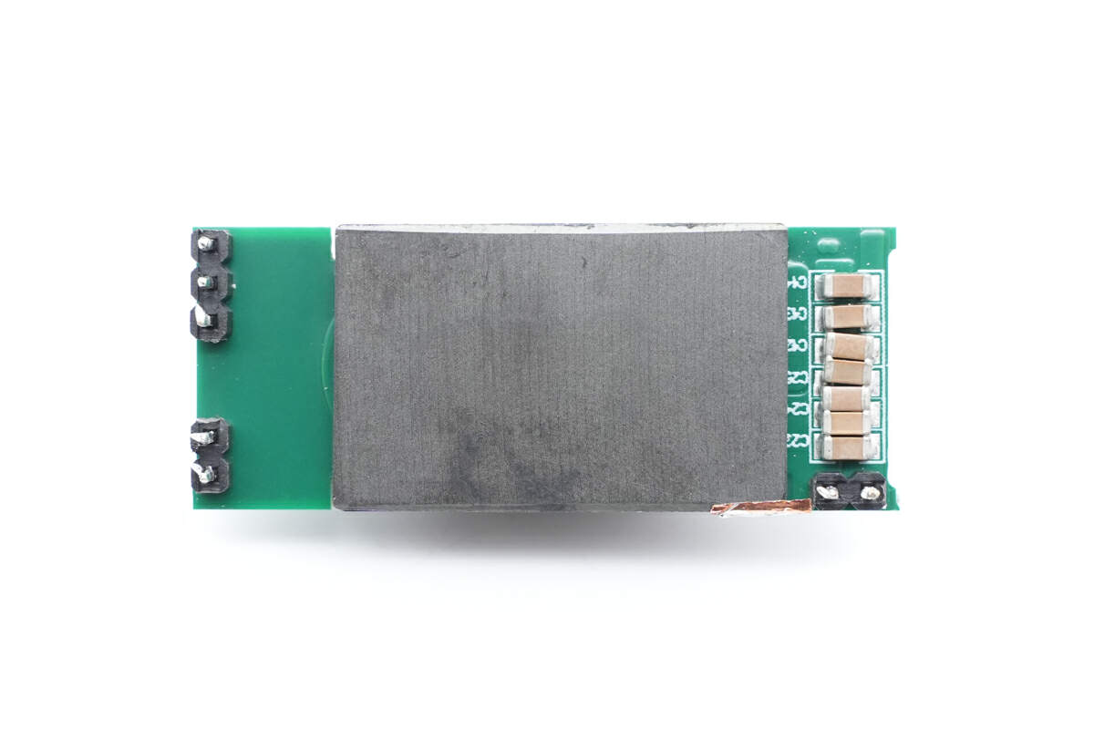
And there are 7 MLCC capacitors connected in parallel for output filtering on the back.
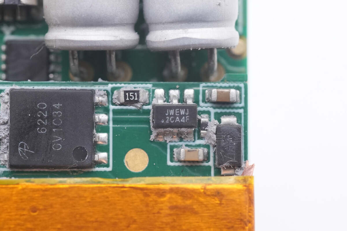
The synchronous rectifier controller is from Joulwatt, model JW7726B, it supports CCM, DCM, QR flyback and ACF active clamping, and has fast turn-off capability. During the start-up process (before VCC is established), it can effectively prevent the gate from being coupled to the turn-on voltage. At present, the cumulative shipment of JW7726 series products is close to 10 million pieces.
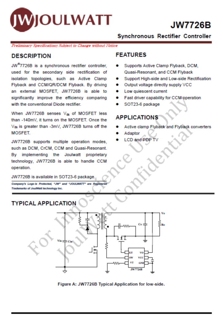
Here is all the information about JW7726.
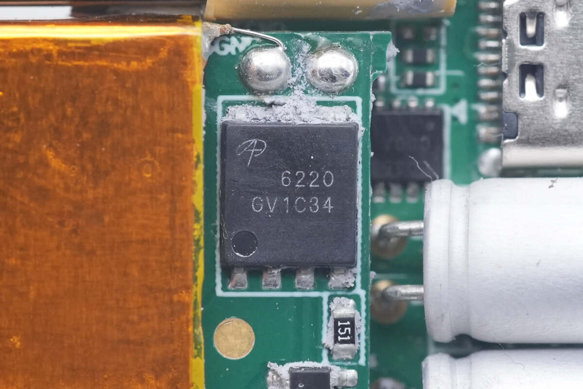
The synchronous rectifier MOSFET is from AOS and adopts DFN5 x 6 package. 100V 6.2mΩ. Model is AON6220.
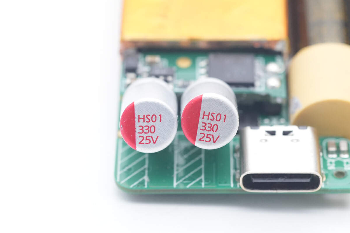
Two solid capacitors for output filtering are both 330μF 25V.
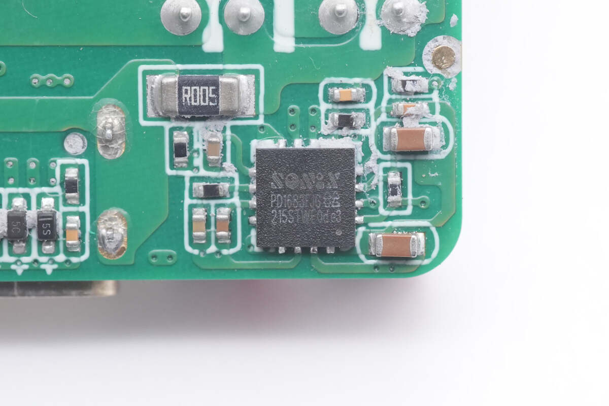
The protocol chip is from Sonix, model SNPD1683, which is a highly integrated USB Type-C port controller that complies with the latest USB Type-C and PD standards. In fact, SNPD1683 has officially obtained Qualcomm QC5 certification, becoming one of the few QC5 fast charge certification protocol chips in the industry.
The SNPD1683 integrates an 8-bit 8051 processor, 16 KB flash memory, a complete Type-C USB-PD transceiver, and a built-in 5V voltage regulator circuit. It also supports 10mV precision adjustment of output voltage and NMOS/PMOS output control.
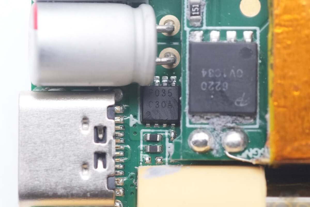
The output VBUS MOSFET is marked with P035.
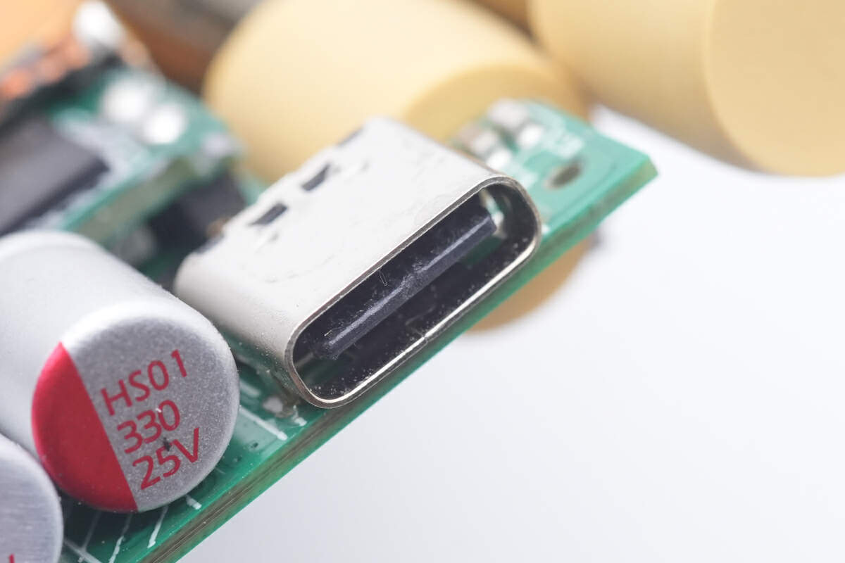
The plastic sheets inside the USB-C socket is black.
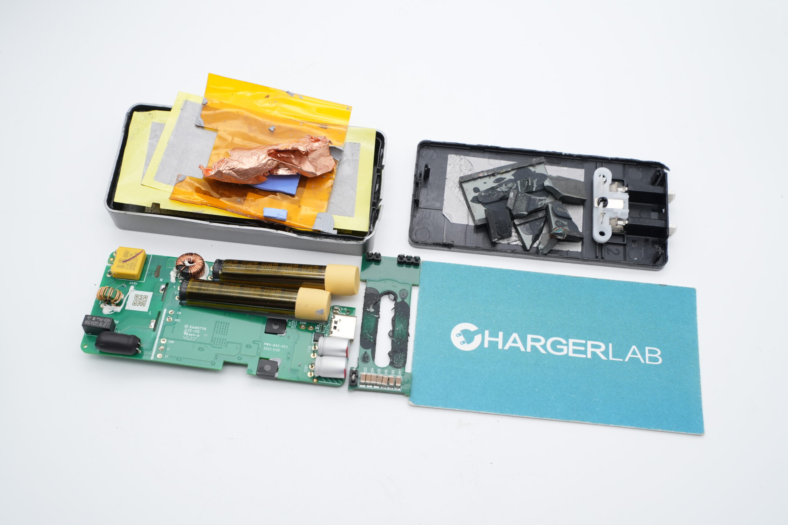
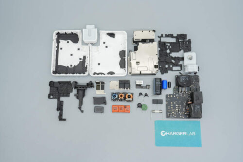
One last look at all the components of this Lenovo 65W Mini GaN Charger.
Summary of ChargerLAB
The Lenovo 65W Mini GaN Charger boasts an ultra-slim design that embodies portability, with a thickness of just 12.7mm facilitated by its foldable prongs and hollow structure. The charger's sole USB-C port supports both 65W PD fast charging output and 5-21V3A PPS fast charging, rendering it a highly practical device that caters to the fast charging demands of both smartphones and computers.
ChargerLAB discovered that the device integrates both a graphite thermal sheet and silicone adhesives to reinforce its heat dissipation properties. Internally, it features a Kiwi KP2202 GaN controller, paired with the Navitas NV6136A GaN power chip. A Joulwatt JW7726B synchronous rectifier controller is soldered onto the planar transformer. Moreover, it boasts two cylindrical capacitors in combination with the hollow design to reduce thickness, and with high-voltage filter capacitors from BERYL, the device exhibits a compact internal configuration.
Related Articles:
1. Teardown of Realme 50W Mini SuperDart Charger (Ultra-thin)
2. Teardown of Lenovo Legion 135W/C135 USB-C GaN Charger
3. WiFi6E Standard | Lenovo Launched ThinkBook Wireless Dock at CES2023


