Introduction
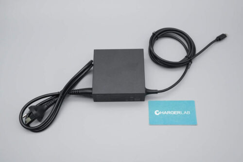
ChargerLAB got an original GaN charger for 100W laptops from Lenovo. This charger is designed with its own cable, and the length of the cable is about 1.8 meters (5.9 feet). It supports 20V 5A PD fast charging and 5-21V 3A PPS fast charging. It is also compatible with phones.
Next, we are going to take it apart to see its internal components and structure.
Product Appearance
![Teardown of Lenovo 100W GaN Charger for Laptops (ADL100UDGC3A)-Chargerlab](https://www.chargerlab.com/wp-content/uploads/2024/07/2024072902225230.jpeg)
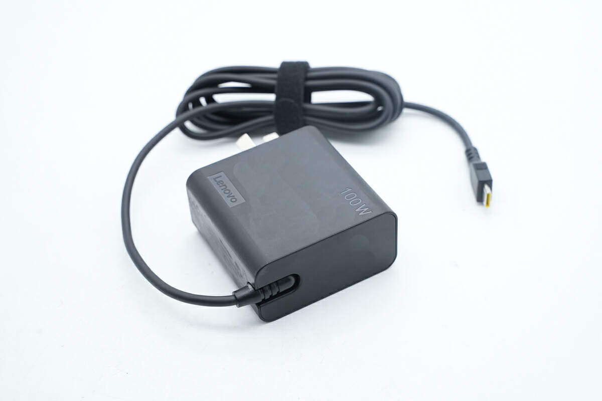
The charger is black. It benefits from the use of GaN technology so it is small in size.
![Teardown of Lenovo 100W GaN Charger for Laptops (ADL100UDGC3A)-Chargerlab](https://www.chargerlab.com/wp-content/uploads/2024/07/2024072902225211.jpeg)
Its case is made of fire-retardant PC with a matte surface.
![Teardown of Lenovo 100W GaN Charger for Laptops (ADL100UDGC3A)-Chargerlab](https://www.chargerlab.com/wp-content/uploads/2024/07/2024072902225699.jpeg)
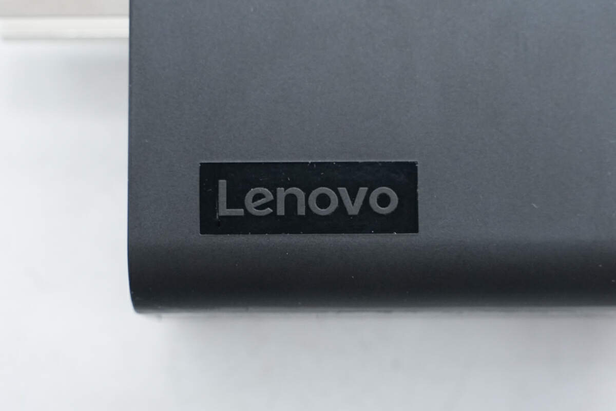
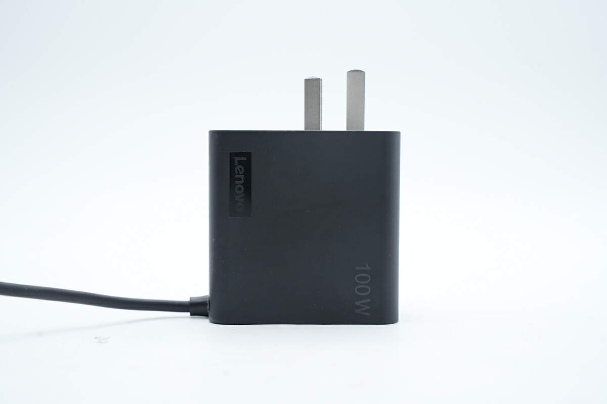
There is a Lenovo logo on the front.
![Teardown of Lenovo 100W GaN Charger for Laptops (ADL100UDGC3A)-Chargerlab](https://www.chargerlab.com/wp-content/uploads/2024/07/2024072902225171.jpeg)
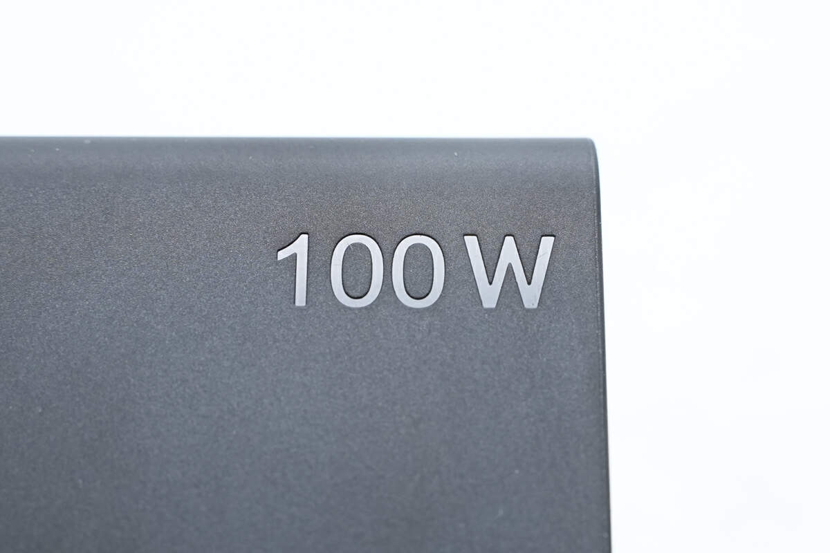
There is the word "100W" here, indicating the maximum output power of this charger.
![Teardown of Lenovo 100W GaN Charger for Laptops (ADL100UDGC3A)-Chargerlab](https://www.chargerlab.com/wp-content/uploads/2024/07/2024072902225116.jpeg)
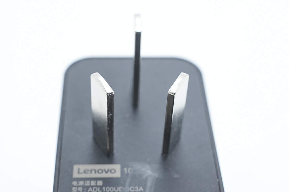
It adopts a three-prong design.
![Teardown of Lenovo 100W GaN Charger for Laptops (ADL100UDGC3A)-Chargerlab](https://www.chargerlab.com/wp-content/uploads/2024/07/2024072902225084.jpeg)
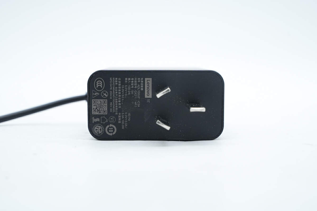
The specs info are printed on the input panel.
![Teardown of Lenovo 100W GaN Charger for Laptops (ADL100UDGC3A)-Chargerlab](https://www.chargerlab.com/wp-content/uploads/2024/07/2024072902225233.jpeg)
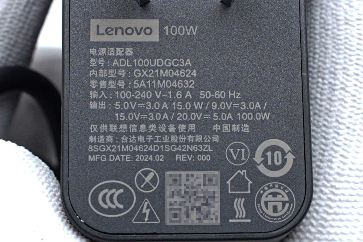
Model is ADL100UDGC3A. It can support input of 100-240V 1.6A 50/60Hz. It can support output of 5V3A, 9V3A, 15V3A, and 20V5A.
![Teardown of Lenovo 100W GaN Charger for Laptops (ADL100UDGC3A)-Chargerlab](https://www.chargerlab.com/wp-content/uploads/2024/07/2024072902225951.jpeg)
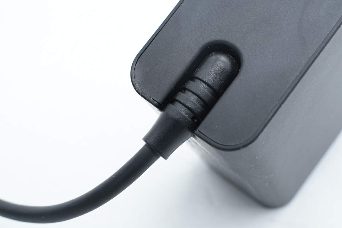
There is a groove at the connection between the output cable and the adapter for protection.
![Teardown of Lenovo 100W GaN Charger for Laptops (ADL100UDGC3A)-Chargerlab](https://www.chargerlab.com/wp-content/uploads/2024/07/2024072902225214.jpeg)
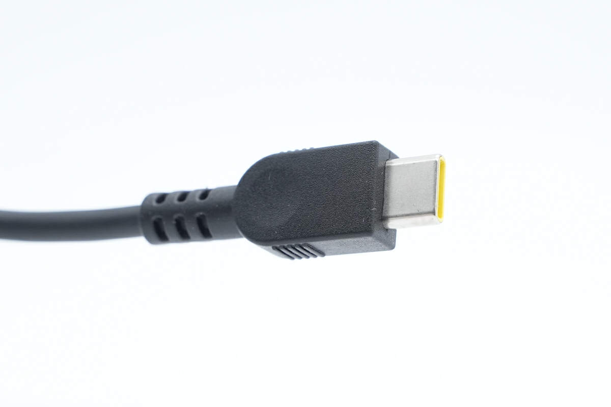
The case of the USB-C connector is equipped with a circular groove to facilitate user plugging and unplugging.
![Teardown of Lenovo 100W GaN Charger for Laptops (ADL100UDGC3A)-Chargerlab](https://www.chargerlab.com/wp-content/uploads/2024/07/2024072902225139.jpeg)
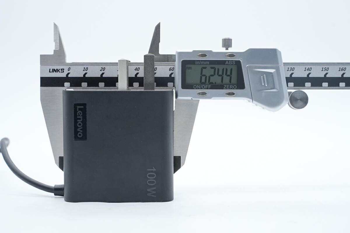
The length of it is about 62 mm (2.44 inches).
![Teardown of Lenovo 100W GaN Charger for Laptops (ADL100UDGC3A)-Chargerlab](https://www.chargerlab.com/wp-content/uploads/2024/07/2024072902225194.jpeg)
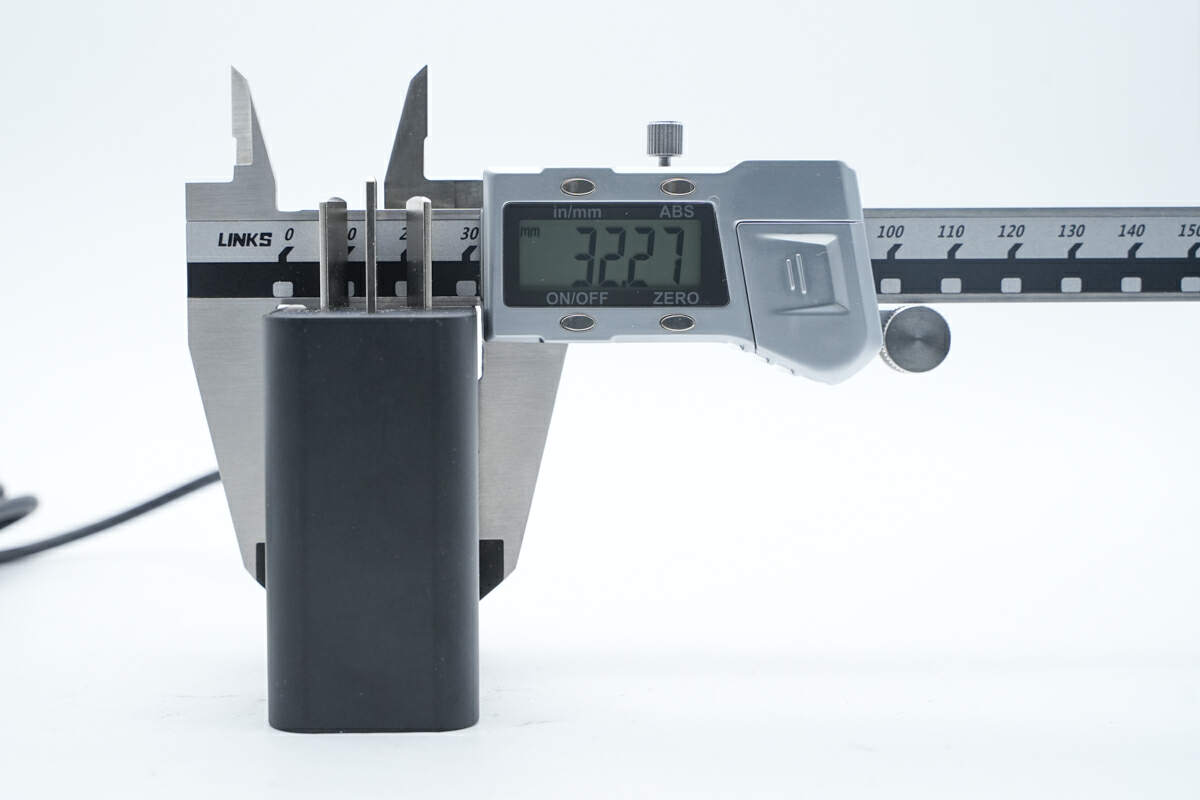
The thickness is about 32 mm (1.26 inches).
![Teardown of Lenovo 100W GaN Charger for Laptops (ADL100UDGC3A)-Chargerlab](https://www.chargerlab.com/wp-content/uploads/2024/07/2024072902225627.jpeg)
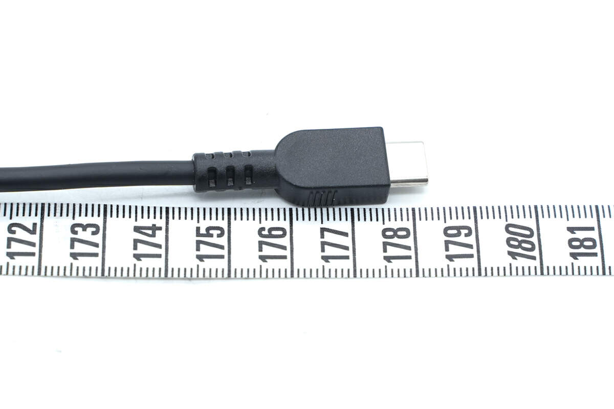
The length of the output cable is about 178 cm (70.079 inches).
![Teardown of Lenovo 100W GaN Charger for Laptops (ADL100UDGC3A)-Chargerlab](https://www.chargerlab.com/wp-content/uploads/2024/07/2024072902225674.jpeg)
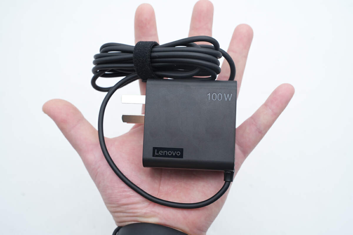
That's how big it is in the hand.
![Teardown of Lenovo 100W GaN Charger for Laptops (ADL100UDGC3A)-Chargerlab](https://www.chargerlab.com/wp-content/uploads/2024/07/2024072902225217.jpeg)
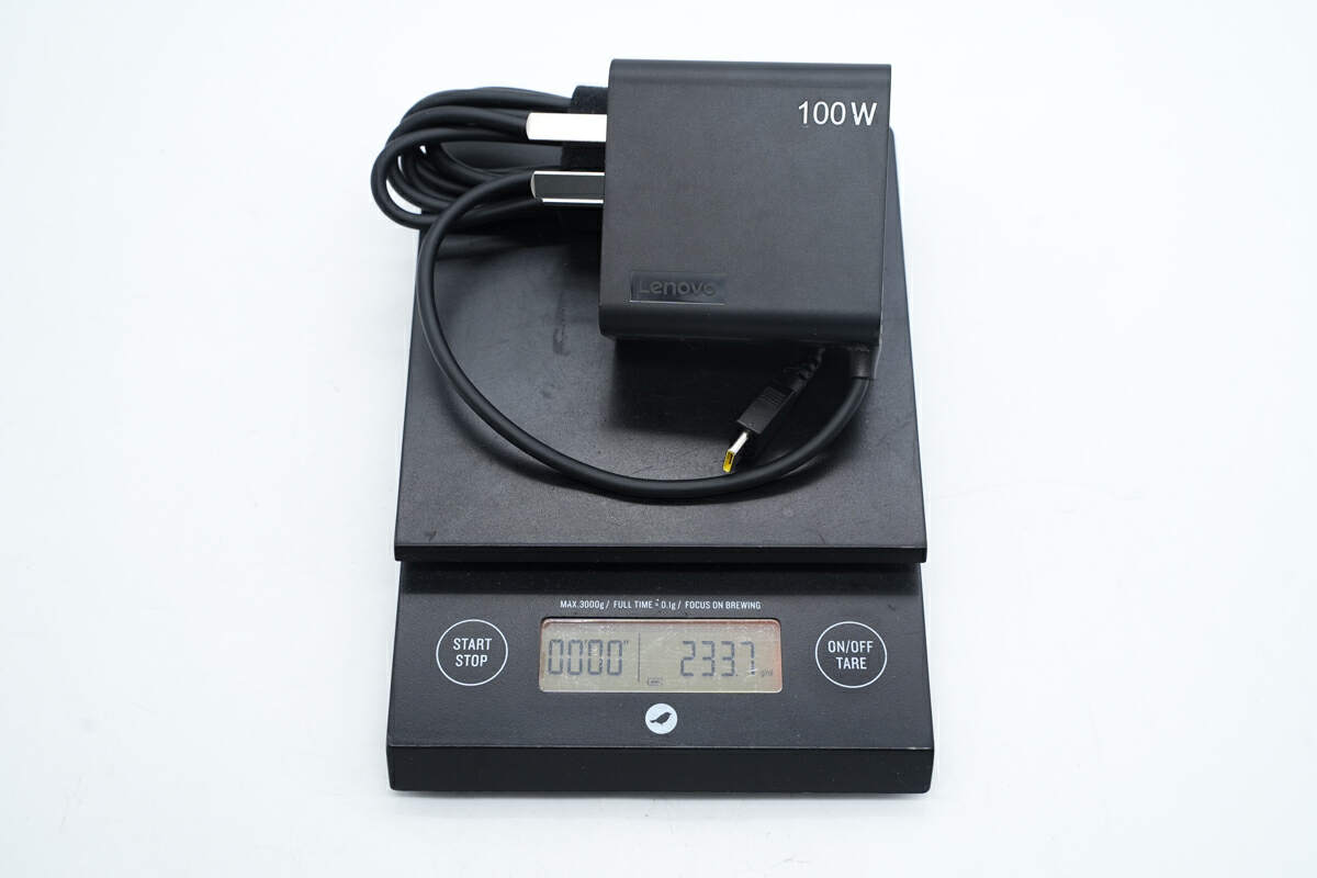
The weight is about 234 g (8.25 oz).
![Teardown of Lenovo 100W GaN Charger for Laptops (ADL100UDGC3A)-Chargerlab](https://www.chargerlab.com/wp-content/uploads/2024/07/2024072902225673.jpeg)
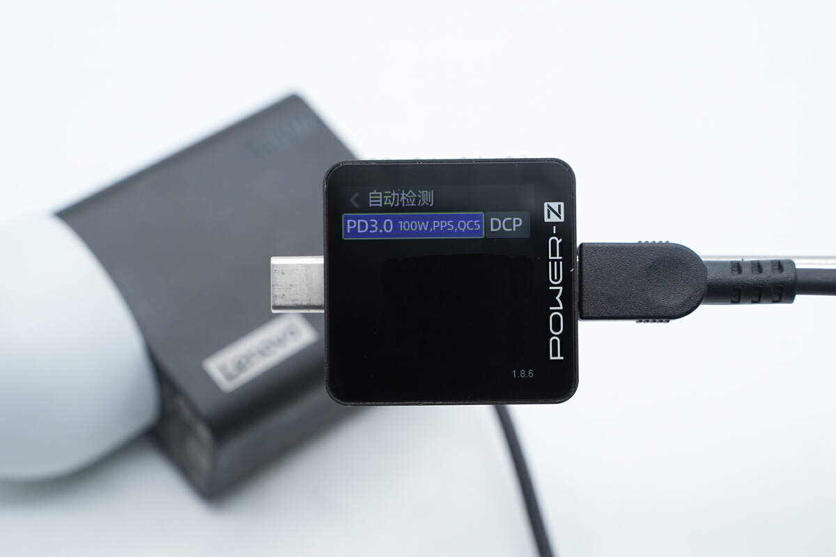
The ChargerLAB POWER-Z KM003C shows that USB-C can support PD3.0, PPS, QC5, and DCP charging protocols.
![Teardown of Lenovo 100W GaN Charger for Laptops (ADL100UDGC3A)-Chargerlab](https://www.chargerlab.com/wp-content/uploads/2024/07/2024072902225748.jpeg)
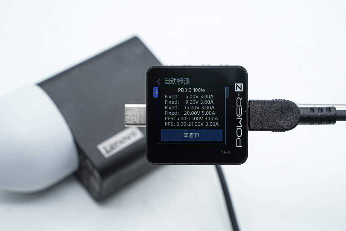
And it has four fixed PDOs of 5V3A, 9V3A, 15V3A, 20V5A, and two sets of PPS, which are 5-11V3A and 5-21V3A.
Teardown
Next, let's start to take it apart to see its internal components and structure.
![Teardown of Lenovo 100W GaN Charger for Laptops (ADL100UDGC3A)-Chargerlab](https://www.chargerlab.com/wp-content/uploads/2024/07/2024072902230022.jpeg)
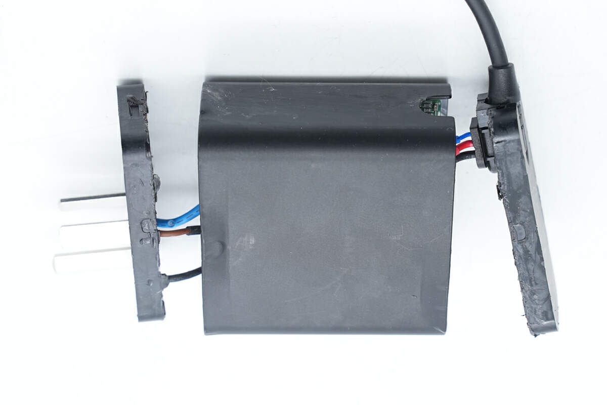
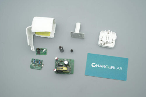
First, remove the input and output covers.
![Teardown of Lenovo 100W GaN Charger for Laptops (ADL100UDGC3A)-Chargerlab](https://www.chargerlab.com/wp-content/uploads/2024/07/2024072902230087.jpeg)
The input wires are connected by soldering.
![Teardown of Lenovo 100W GaN Charger for Laptops (ADL100UDGC3A)-Chargerlab](https://www.chargerlab.com/wp-content/uploads/2024/07/2024072902230093.jpeg)
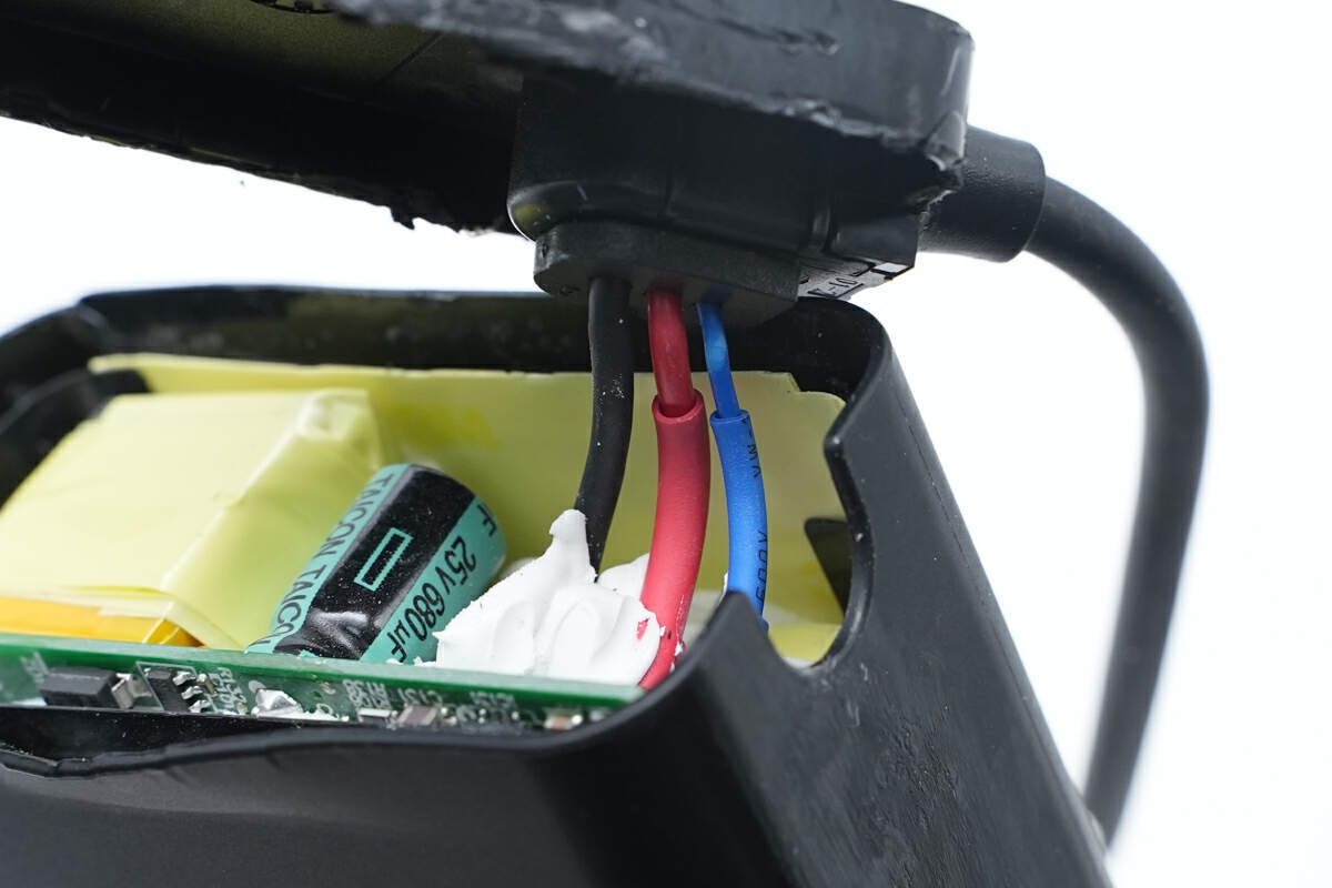
The output wires are also connected by soldering.
![Teardown of Lenovo 100W GaN Charger for Laptops (ADL100UDGC3A)-Chargerlab](https://www.chargerlab.com/wp-content/uploads/2024/07/2024072902225284.jpeg)
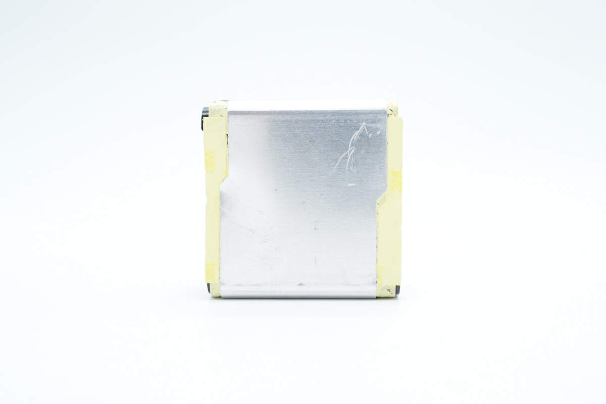
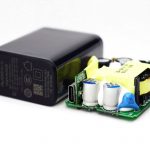
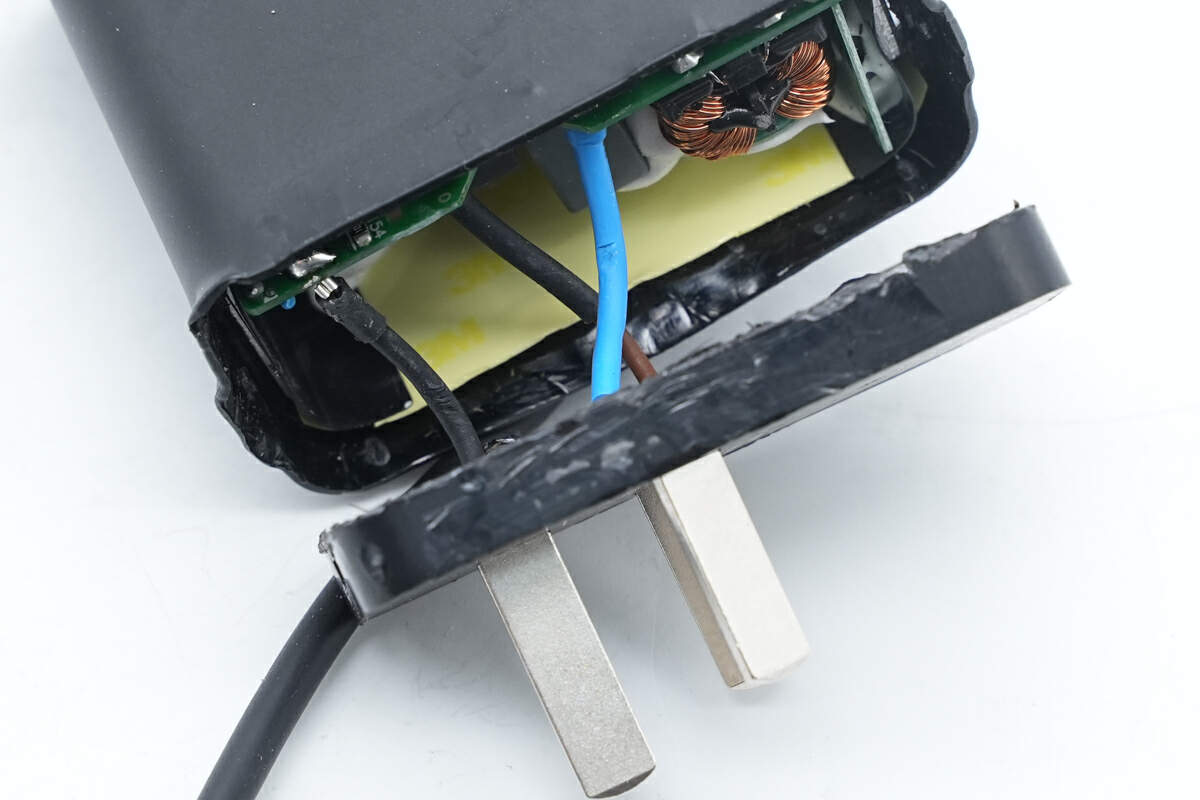
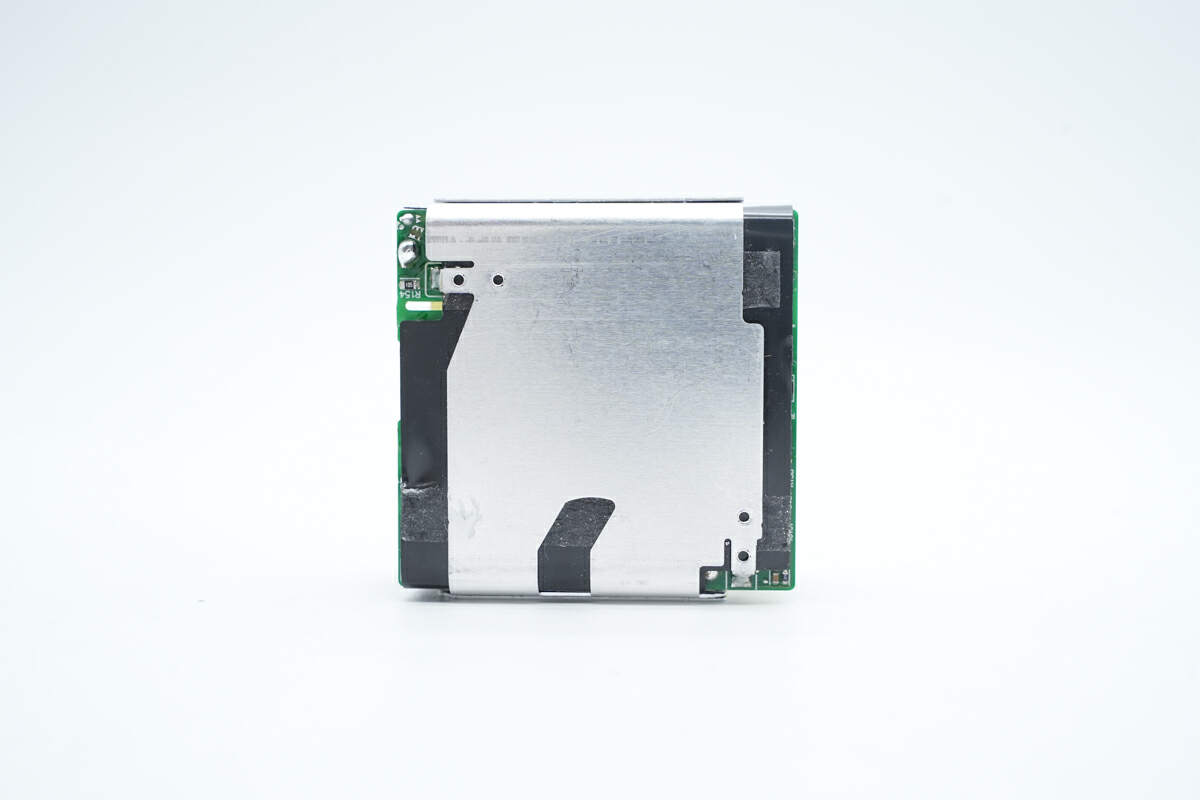
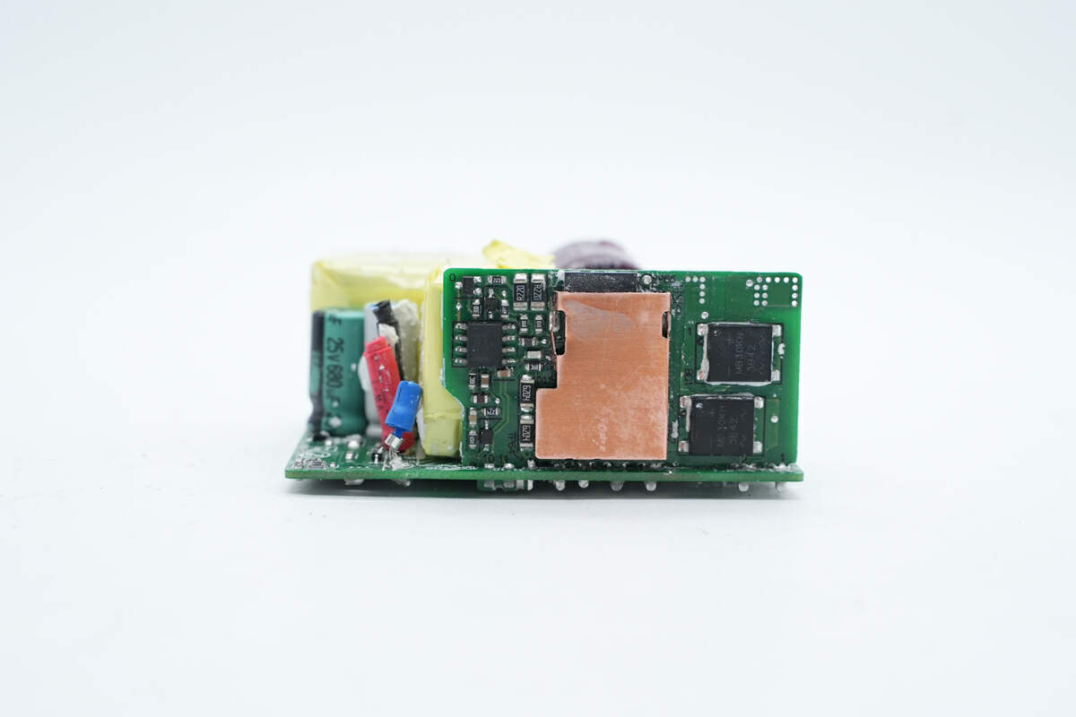
Cut off the connecting wires and take out the PCBA module. The PCBA module is wrapped with aluminum sheets for heat dissipation.
![Teardown of Lenovo 100W GaN Charger for Laptops (ADL100UDGC3A)-Chargerlab](https://www.chargerlab.com/wp-content/uploads/2024/07/2024072902230052.jpeg)
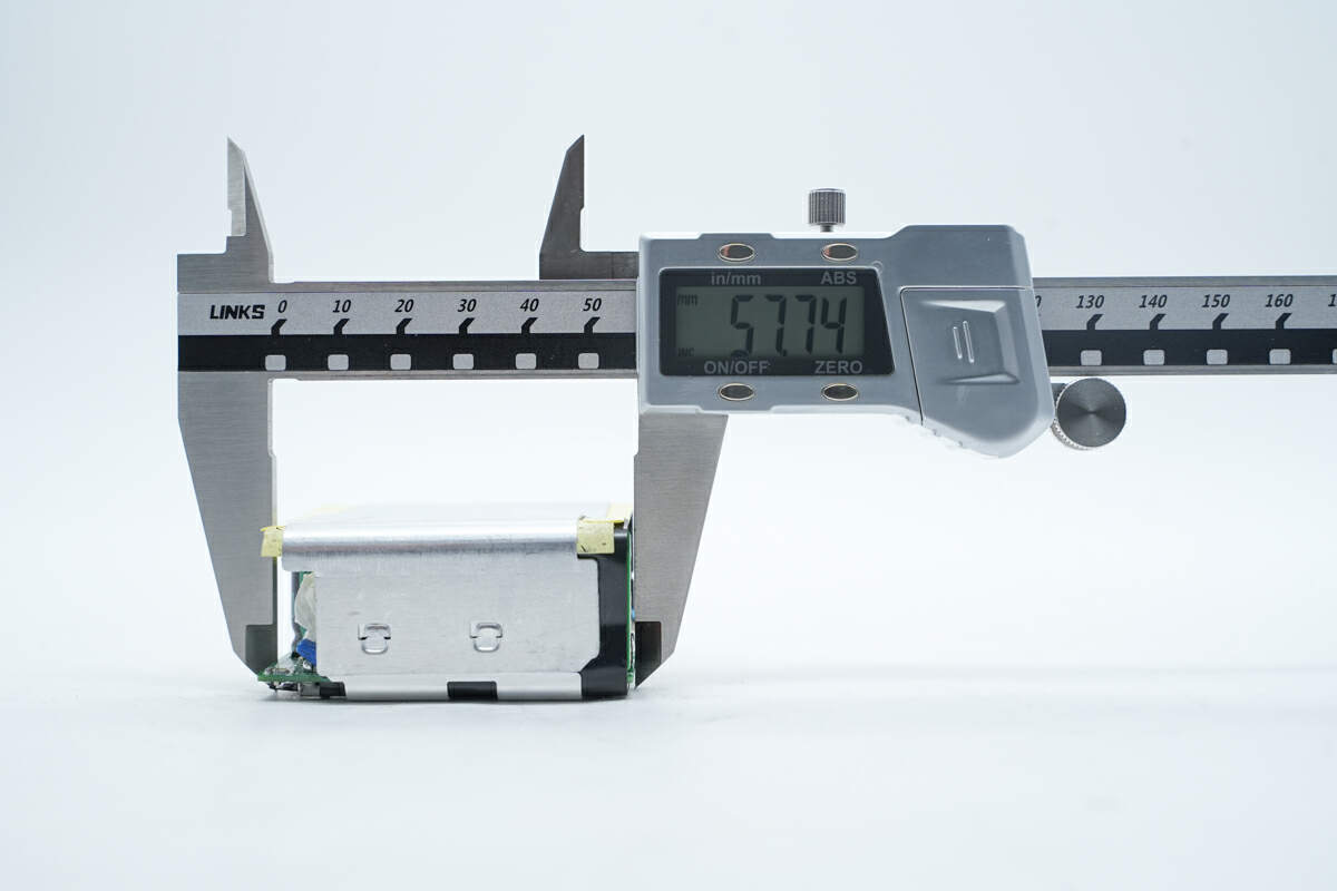
The length of the PCBA module is about 58 mm (2.28 inches).
![Teardown of Lenovo 100W GaN Charger for Laptops (ADL100UDGC3A)-Chargerlab](https://www.chargerlab.com/wp-content/uploads/2024/07/2024072902225120.jpeg)
The width is about 58 mm (2.28 inches).
![Teardown of Lenovo 100W GaN Charger for Laptops (ADL100UDGC3A)-Chargerlab](https://www.chargerlab.com/wp-content/uploads/2024/07/2024072902230021.jpeg)
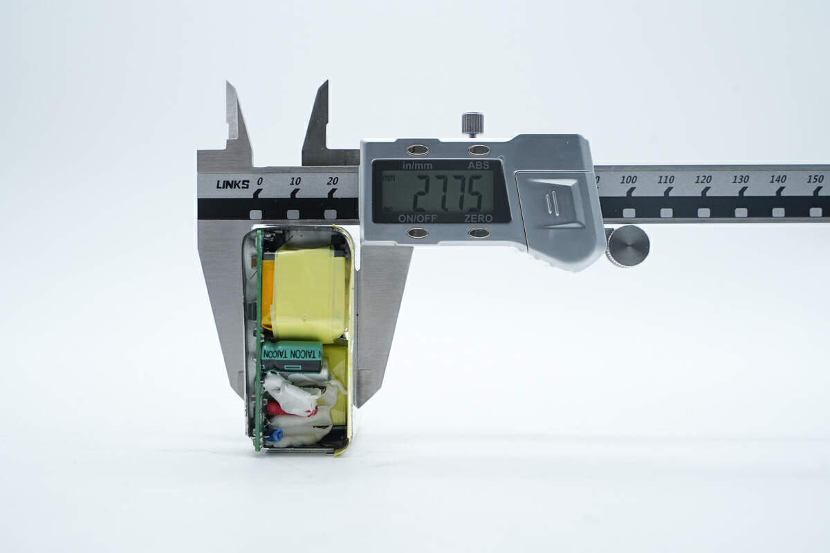
The thickness is about 28 mm (1.1 inches).
![Teardown of Lenovo 100W GaN Charger for Laptops (ADL100UDGC3A)-Chargerlab](https://www.chargerlab.com/wp-content/uploads/2024/07/2024072902225193.jpeg)
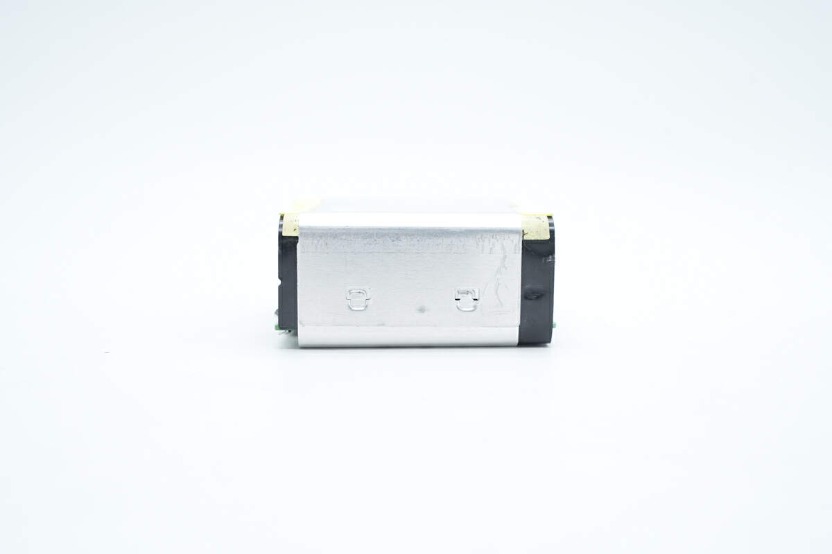
The aluminum sheets are fixed with clips.
![Teardown of Lenovo 100W GaN Charger for Laptops (ADL100UDGC3A)-Chargerlab](https://www.chargerlab.com/wp-content/uploads/2024/07/2024072902225140.jpeg)
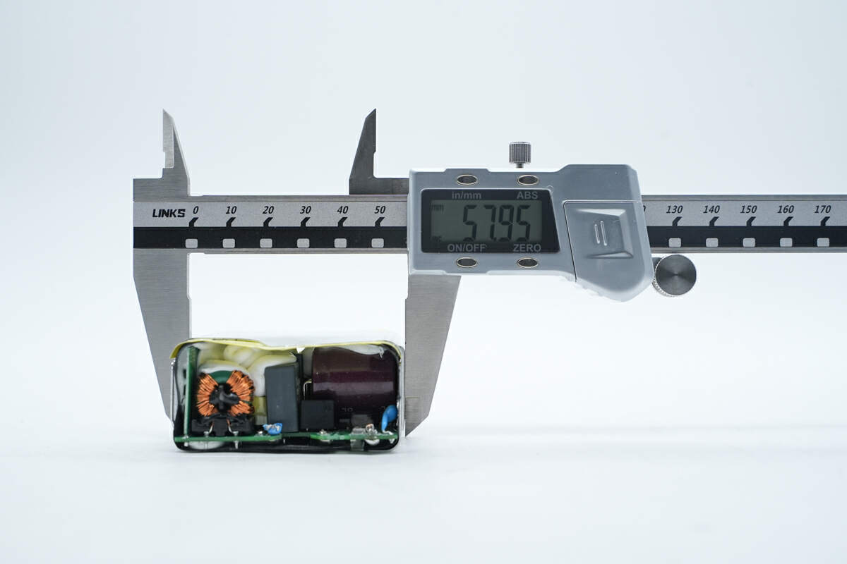
The heat sinks are soldered to the PCBA module.
![Teardown of Lenovo 100W GaN Charger for Laptops (ADL100UDGC3A)-Chargerlab](https://www.chargerlab.com/wp-content/uploads/2024/07/2024072902225742.jpeg)
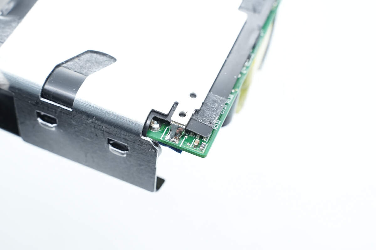
This is the solder joint for the heat sink.
![Teardown of Lenovo 100W GaN Charger for Laptops (ADL100UDGC3A)-Chargerlab](https://www.chargerlab.com/wp-content/uploads/2024/07/2024072902225827.jpeg)
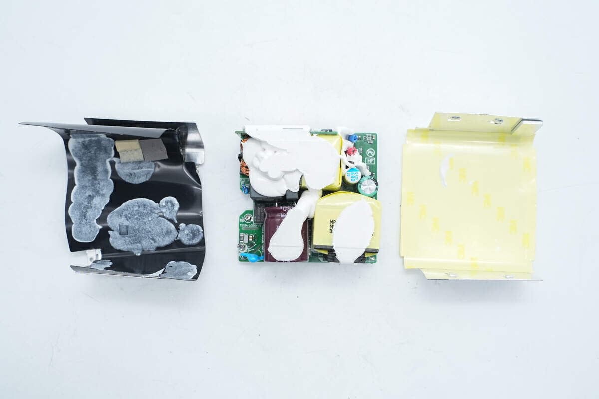
Remove the heat sinks. There is a mylar sheet between the heat sink and the PCBA module for insulation. The PCBA module is filled with potting compound for heat dissipation.
![Teardown of Lenovo 100W GaN Charger for Laptops (ADL100UDGC3A)-Chargerlab](https://www.chargerlab.com/wp-content/uploads/2024/07/2024072902225546.jpeg)
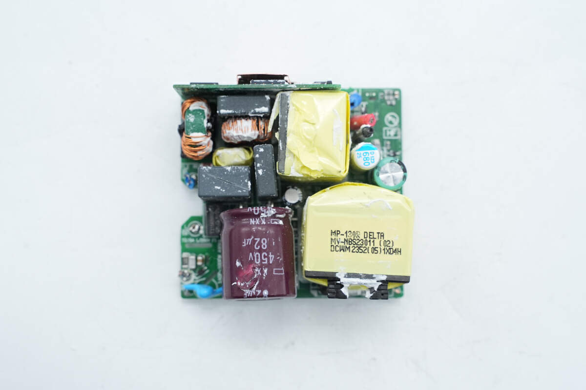
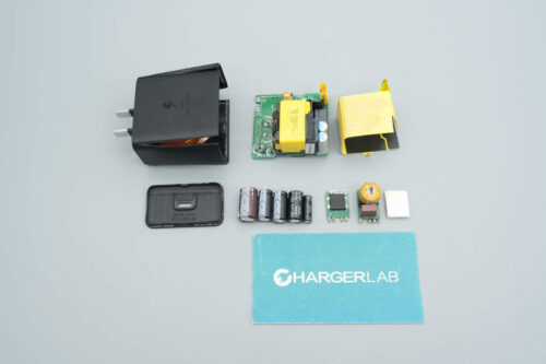
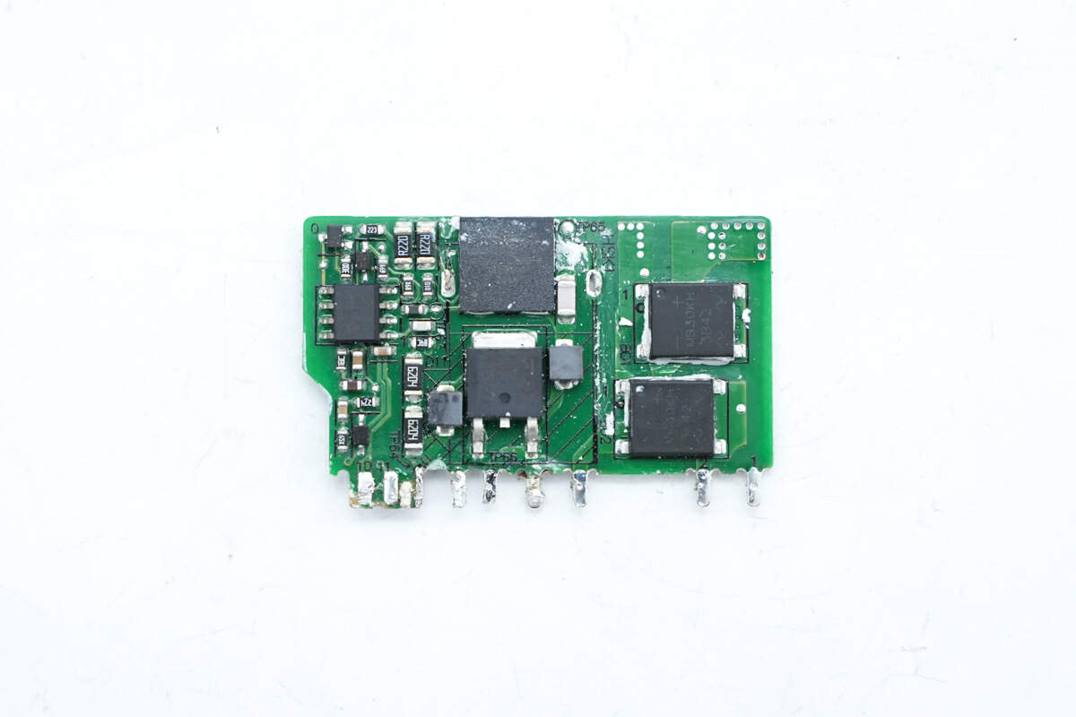
The fuse, safety X2 capacitor, common mode choke, bridge rectifier, PFC boost inductor, capacitor, and transformer are on the front of the PCBA module.
![Teardown of Lenovo 100W GaN Charger for Laptops (ADL100UDGC3A)-Chargerlab](https://www.chargerlab.com/wp-content/uploads/2024/07/2024072902230272.jpeg)
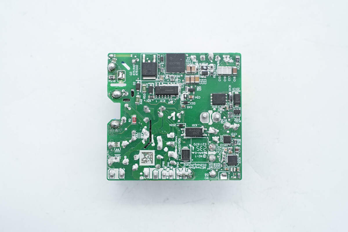
The back of the PCBA module has a hybrid-flyback controller, two MOSFETs, a feedback optocoupler, a synchronous rectifier controller, a synchronous rectifier, and a protocol chip.
ChargerLAB found it adopts a PFC+HFB hybrid flyback topology, with a wide-range output voltage.
Next, we will take a look at each component starting from the input end.
![Teardown of Lenovo 100W GaN Charger for Laptops (ADL100UDGC3A)-Chargerlab](https://www.chargerlab.com/wp-content/uploads/2024/07/2024072902225365.jpeg)
The fuse, common mode choke, and safety X2 capacitor are at the input end.
![Teardown of Lenovo 100W GaN Charger for Laptops (ADL100UDGC3A)-Chargerlab](https://www.chargerlab.com/wp-content/uploads/2024/07/2024072902224997.jpeg)
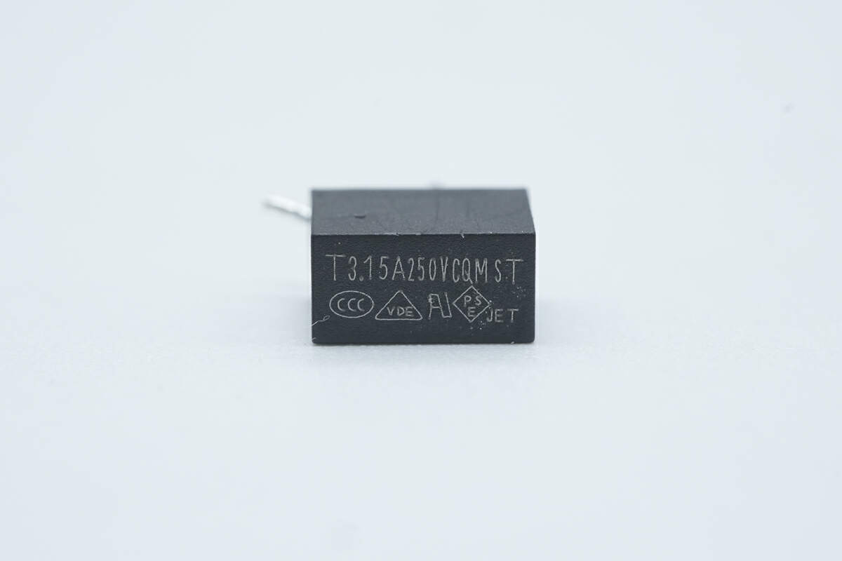
The input fuse is from CONQUER MST series and is used for input overcurrent protection. 3.15A 250V.
![Teardown of Lenovo 100W GaN Charger for Laptops (ADL100UDGC3A)-Chargerlab](https://www.chargerlab.com/wp-content/uploads/2024/07/2024072902230184.jpeg)
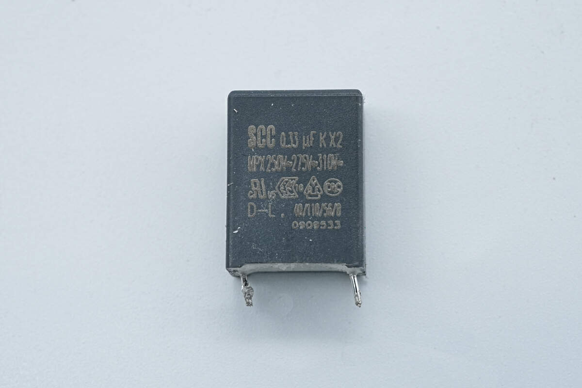
The safety X2 capacitor is from SCC. 0.33μF.
![Teardown of Lenovo 100W GaN Charger for Laptops (ADL100UDGC3A)-Chargerlab](https://www.chargerlab.com/wp-content/uploads/2024/07/2024072902225727.jpeg)
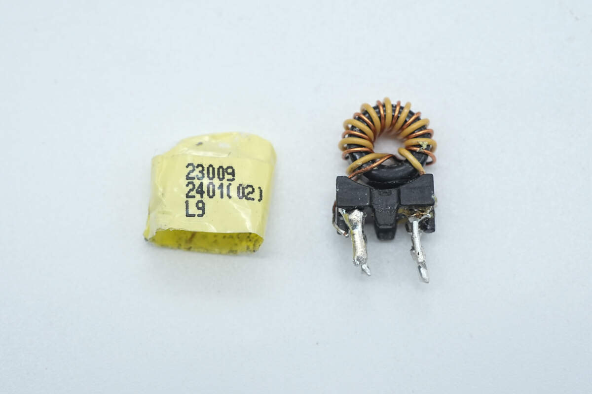
The common mode choke is wound with magnet and insulated wires, and it's also insulated with a bracket and tape.
![Teardown of Lenovo 100W GaN Charger for Laptops (ADL100UDGC3A)-Chargerlab](https://www.chargerlab.com/wp-content/uploads/2024/07/2024072902225768.jpeg)
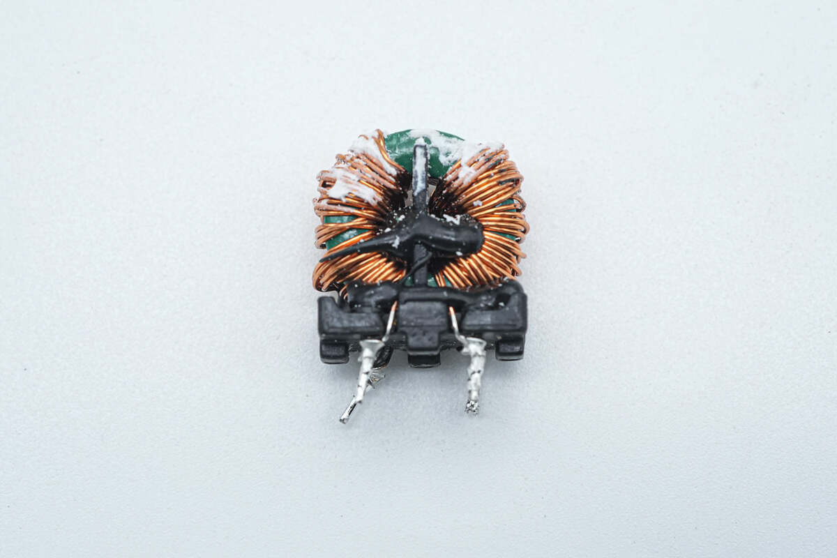
The other common mode choke is also wound with magnet and insulated wires. And it's also insulated with a bracket.
![Teardown of Lenovo 100W GaN Charger for Laptops (ADL100UDGC3A)-Chargerlab](https://www.chargerlab.com/wp-content/uploads/2024/07/2024072902230092-1.jpeg)
The bridge rectifier, PFC controller, PFC MOSFET, and PFC rectifier are fixed on the side of the PCBA module. There are copper sheets and thermal pads corresponding to the MOSFET and rectifier positions to enhance heat dissipation.
![Teardown of Lenovo 100W GaN Charger for Laptops (ADL100UDGC3A)-Chargerlab](https://www.chargerlab.com/wp-content/uploads/2024/07/2024072902230079.jpeg)
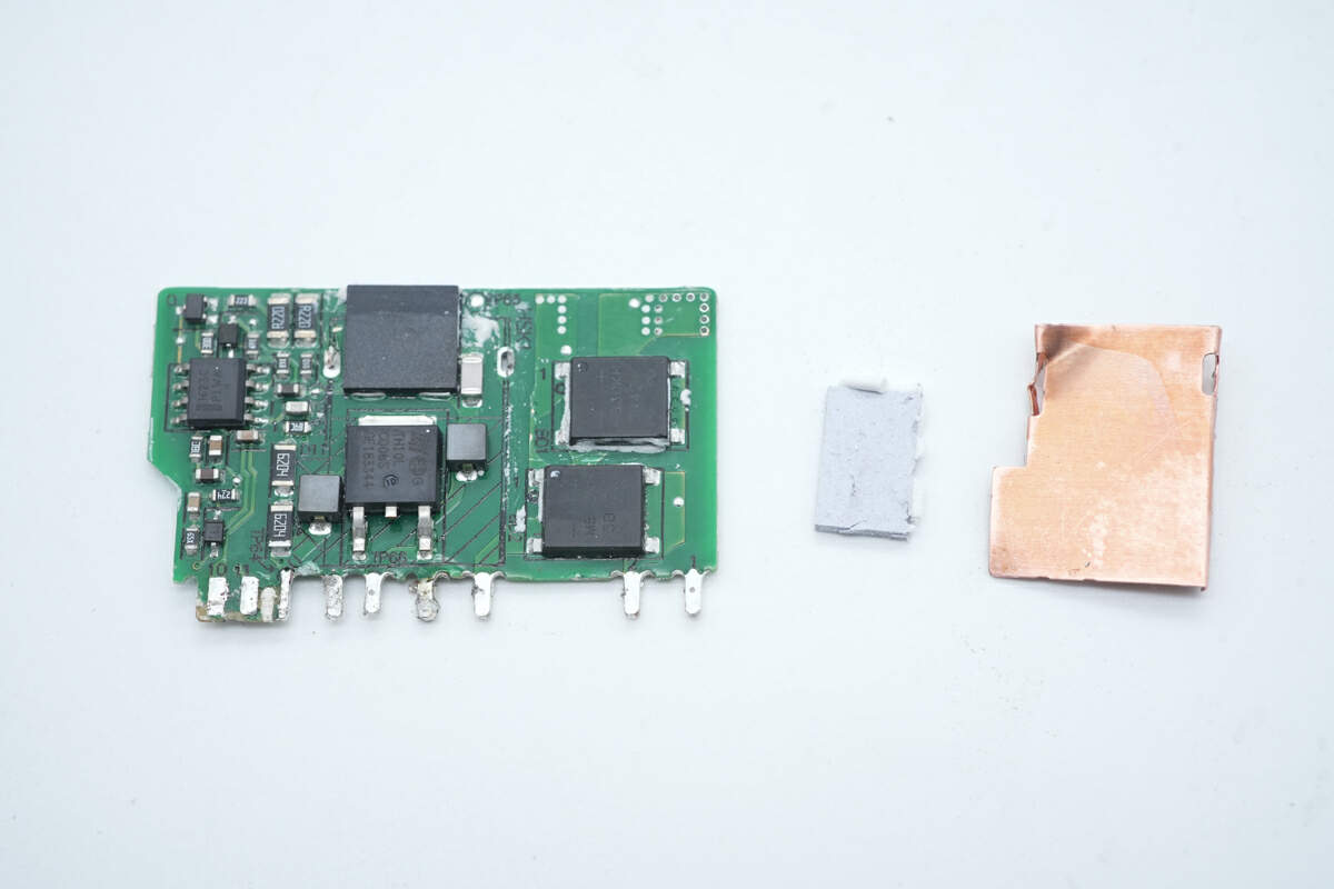
Remove the side small PCB and the copper sheet.
![Teardown of Lenovo 100W GaN Charger for Laptops (ADL100UDGC3A)-Chargerlab](https://www.chargerlab.com/wp-content/uploads/2024/07/2024072902225120-1.jpeg)
The two bridge rectifiers, PFC controller, PFC MOSFET, and PFC rectifier are fixed on the side small PCB.
![Teardown of Lenovo 100W GaN Charger for Laptops (ADL100UDGC3A)-Chargerlab](https://www.chargerlab.com/wp-content/uploads/2024/07/2024072902225215.jpeg)
There are no components on the back of the small PCB.
![Teardown of Lenovo 100W GaN Charger for Laptops (ADL100UDGC3A)-Chargerlab](https://www.chargerlab.com/wp-content/uploads/2024/07/2024072902225946.jpeg)
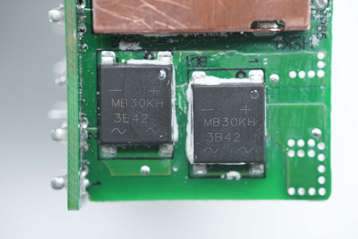
These are the two bridge rectifiers. Model is MB30KH. 3A 1000V.
![Teardown of Lenovo 100W GaN Charger for Laptops (ADL100UDGC3A)-Chargerlab](https://www.chargerlab.com/wp-content/uploads/2024/07/2024072902225721.jpeg)
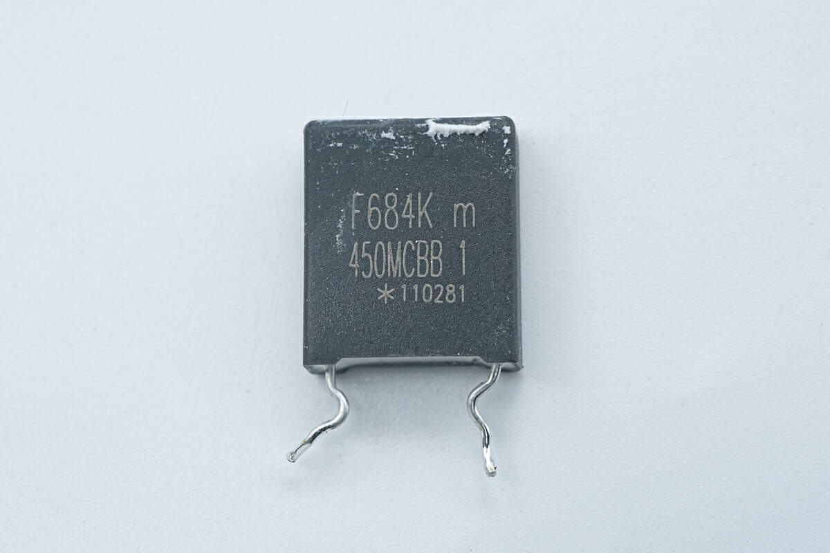
The specification of this thin film capacitor is 0.68μF.
![Teardown of Lenovo 100W GaN Charger for Laptops (ADL100UDGC3A)-Chargerlab](https://www.chargerlab.com/wp-content/uploads/2024/07/2024072902225516.jpeg)
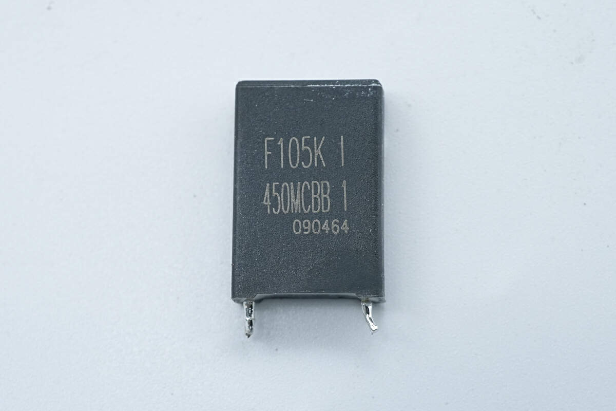
The other film capacitor has a specification of 1μF.
![Teardown of Lenovo 100W GaN Charger for Laptops (ADL100UDGC3A)-Chargerlab](https://www.chargerlab.com/wp-content/uploads/2024/07/2024072902225950.jpeg)
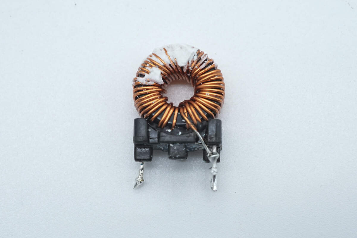
The filter inductor is wounded with a magnetic ring and insulated by a bracket.
![Teardown of Lenovo 100W GaN Charger for Laptops (ADL100UDGC3A)-Chargerlab](https://www.chargerlab.com/wp-content/uploads/2024/07/2024072902225374.jpeg)
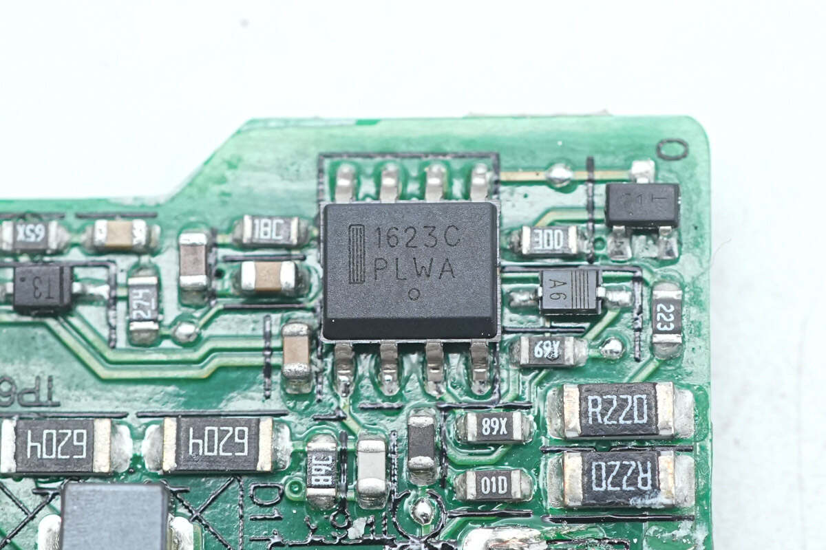
The PFC controller is from Onsemi. It is based on an innovative Valley Synchronized Frequency Fold-back (VSFF) method, it operates in critical conduction mode (CrM) until the power drops below a threshold level. The VSFF maximizes the efficiency at both nominal and light loads. Model is NCP1623.
It will enter discontinuous conduction mode (DCM) with increased dead-time as the load further decays (frequency foldback).
![Teardown of Lenovo 100W GaN Charger for Laptops (ADL100UDGC3A)-Chargerlab](https://www.chargerlab.com/wp-content/uploads/2024/07/2024072902225267.jpeg)
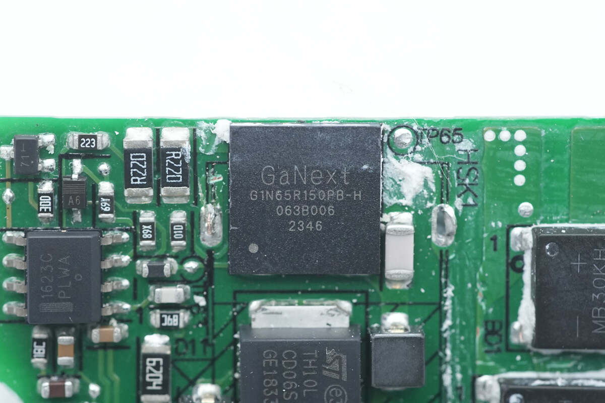
The PFC MOSFET is from GaNext and adopts PQFN8x8 package. It has a high repetitive input voltage tolerance of ±20V. Model is G1N65R150PB-H. 650V 150mΩ.
![Teardown of Lenovo 100W GaN Charger for Laptops (ADL100UDGC3A)-Chargerlab](https://www.chargerlab.com/wp-content/uploads/2024/07/2024072902230139.png)
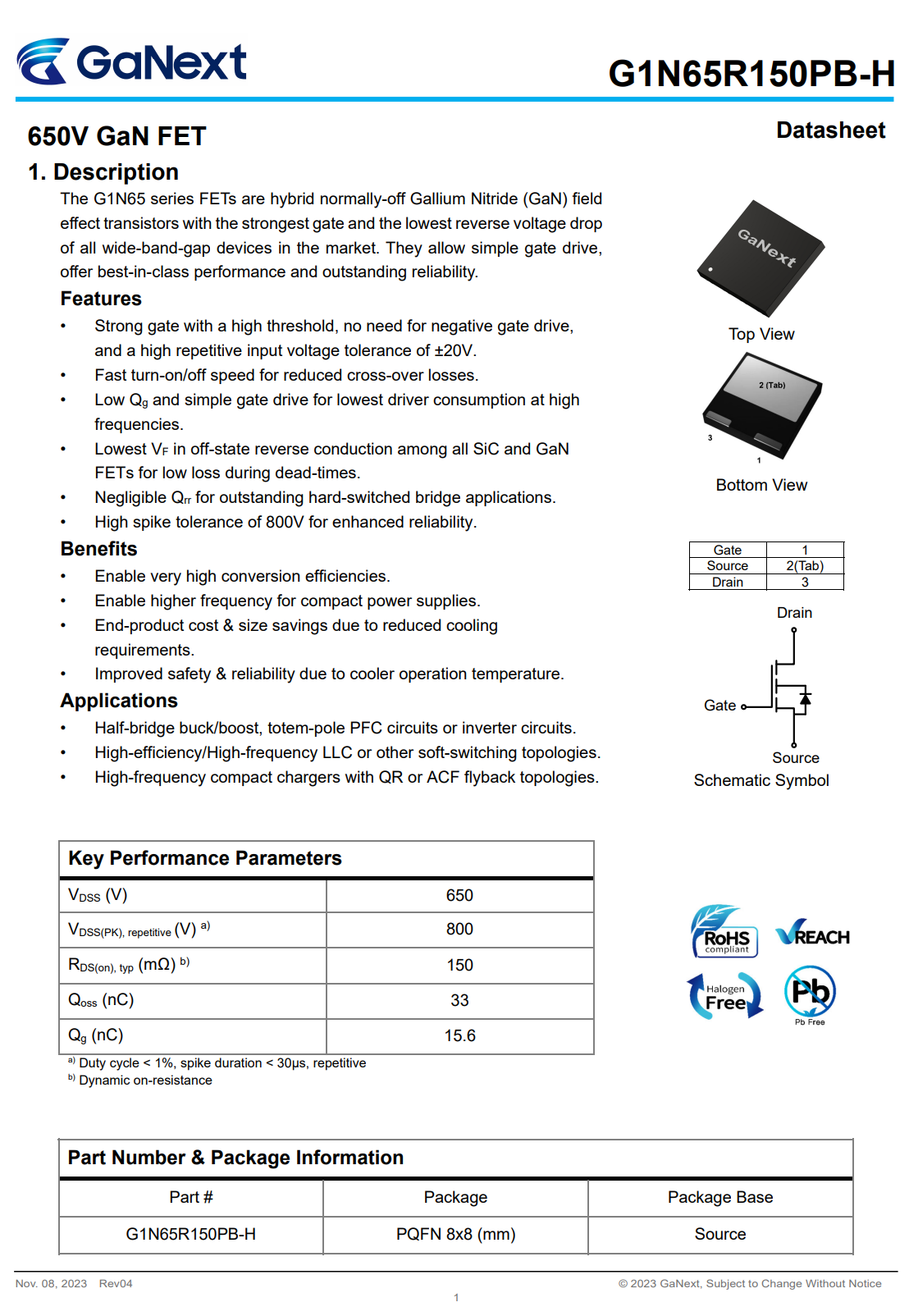
Here is information about GaNext G1N65R150PB-H.
![Teardown of Lenovo 100W GaN Charger for Laptops (ADL100UDGC3A)-Chargerlab](https://www.chargerlab.com/wp-content/uploads/2024/07/2024072902225755.jpeg)
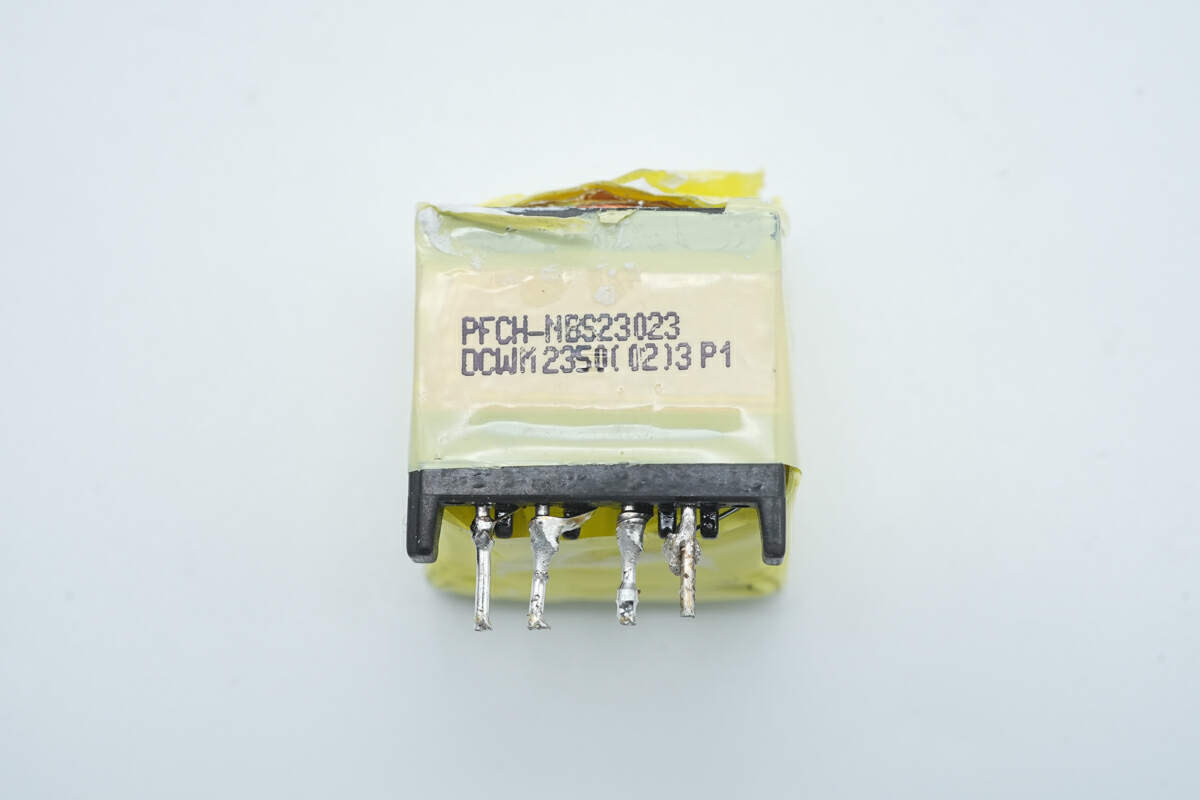
The magnetic core of the PFC boost inductor is wrapped with copper foil shield and insulated with tape.
![Teardown of Lenovo 100W GaN Charger for Laptops (ADL100UDGC3A)-Chargerlab](https://www.chargerlab.com/wp-content/uploads/2024/07/2024072902225628.jpeg)
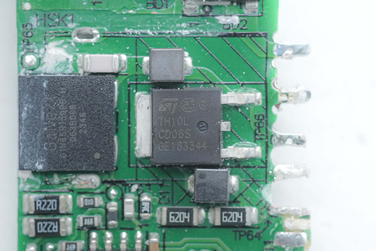
The PFC rectifier is from STMicro and adopts DPAK package. 10A 600V. Model is STTH10LCD06.
![Teardown of Lenovo 100W GaN Charger for Laptops (ADL100UDGC3A)-Chargerlab](https://www.chargerlab.com/wp-content/uploads/2024/07/2024072902230177.jpeg)
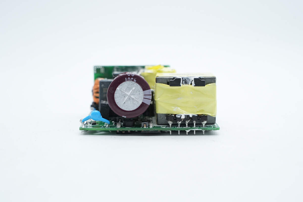
The filter capacitor and transformer are on this side of the PCBA module.
![Teardown of Lenovo 100W GaN Charger for Laptops (ADL100UDGC3A)-Chargerlab](https://www.chargerlab.com/wp-content/uploads/2024/07/2024072902225279.jpeg)
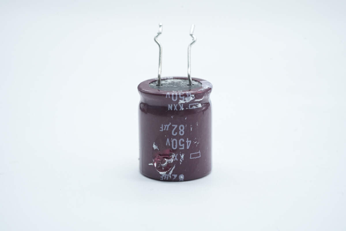
The electrolytic capacitor is from NCC. 450V 82μF.
![Teardown of Lenovo 100W GaN Charger for Laptops (ADL100UDGC3A)-Chargerlab](https://www.chargerlab.com/wp-content/uploads/2024/07/2024072902225772.jpeg)
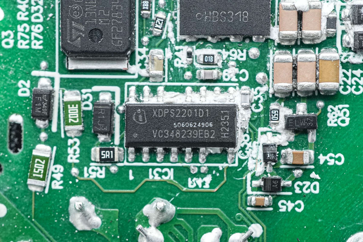
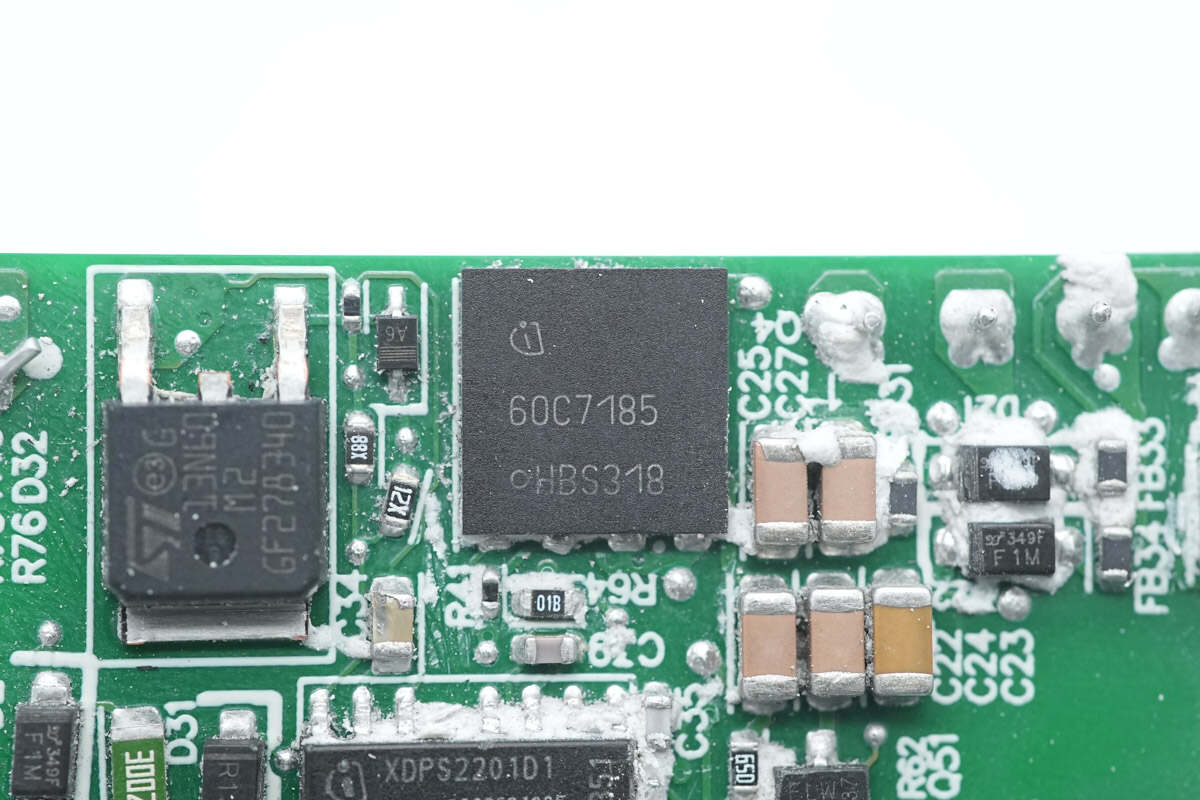
The HFB controller is from Infineon and adopts PG-DSO-14 package. It is a hybrid flyback controller. It integrates 600V high-voltage start-up cell for fast charging, and can drive both high and low-side MOSFETs. And the standby power consumption is less than 75mW. It simplifies the external components. Model is XPDS2201.
![Teardown of Lenovo 100W GaN Charger for Laptops (ADL100UDGC3A)-Chargerlab](https://www.chargerlab.com/wp-content/uploads/2024/07/2024072902230092.jpeg)
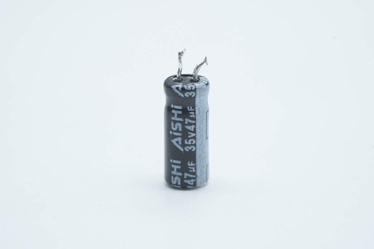
The filter capacitor that supplies power to the master control chip is from AiSHi. 35V 47μF.
![Teardown of Lenovo 100W GaN Charger for Laptops (ADL100UDGC3A)-Chargerlab](https://www.chargerlab.com/wp-content/uploads/2024/07/2024072902225951-1.jpeg)
This MOSFET is from Infineon and adopts ThinPAK8*8 package. 650V 185mΩ. Model is IPL60R185C7.
![Teardown of Lenovo 100W GaN Charger for Laptops (ADL100UDGC3A)-Chargerlab](https://www.chargerlab.com/wp-content/uploads/2024/07/2024072902225927.jpeg)
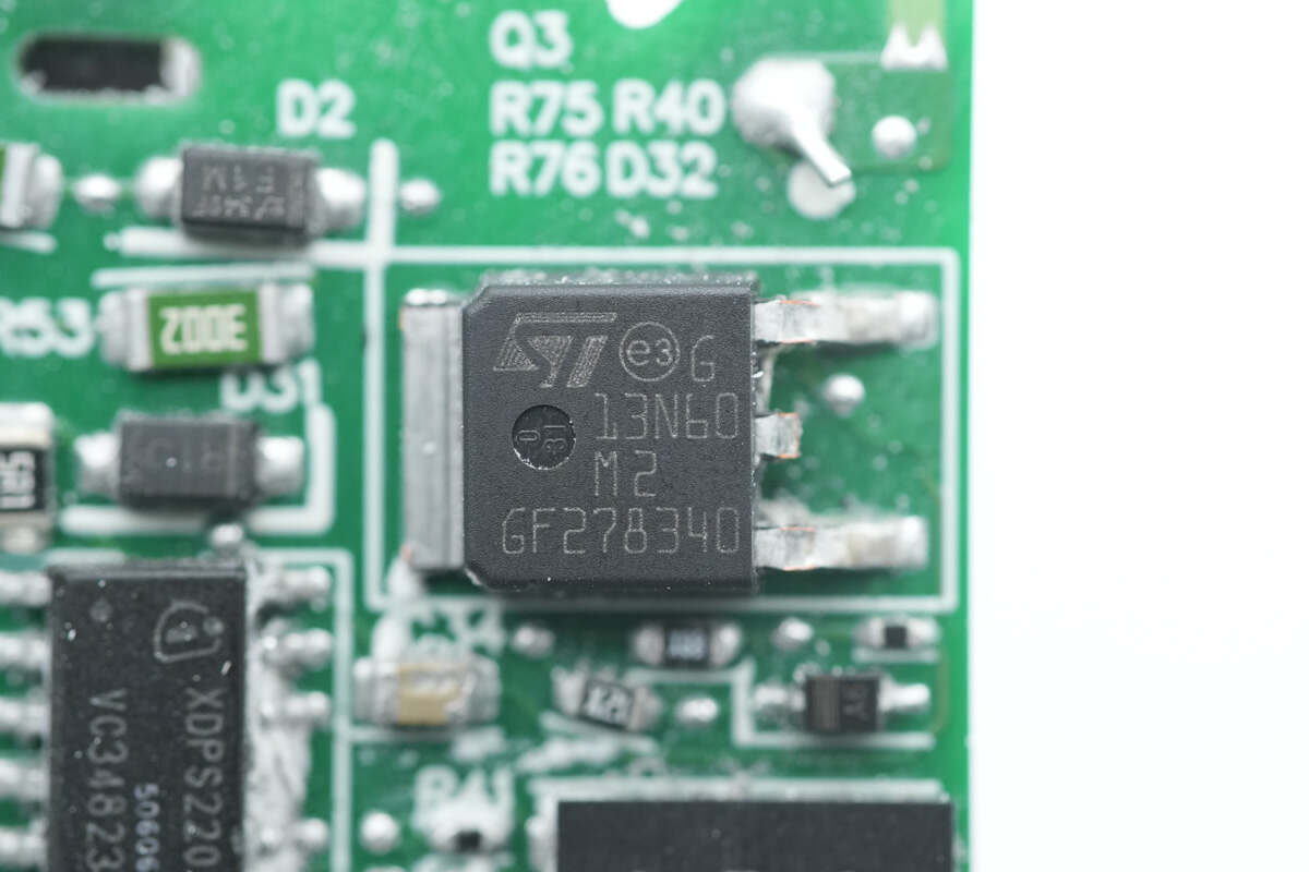
The HFB PMOSFET is from STMicro and adopts DPAK package. Model is STD13N60M2. 650V 380mΩ.
![Teardown of Lenovo 100W GaN Charger for Laptops (ADL100UDGC3A)-Chargerlab](https://www.chargerlab.com/wp-content/uploads/2024/07/2024072902225912.jpeg)
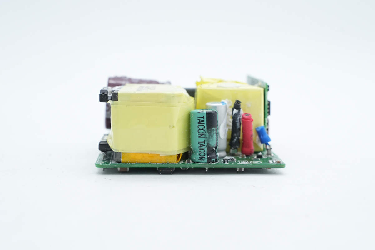
This side has the transformer and the capacitor for output filtering.
![Teardown of Lenovo 100W GaN Charger for Laptops (ADL100UDGC3A)-Chargerlab](https://www.chargerlab.com/wp-content/uploads/2024/07/2024072902225588.jpeg)
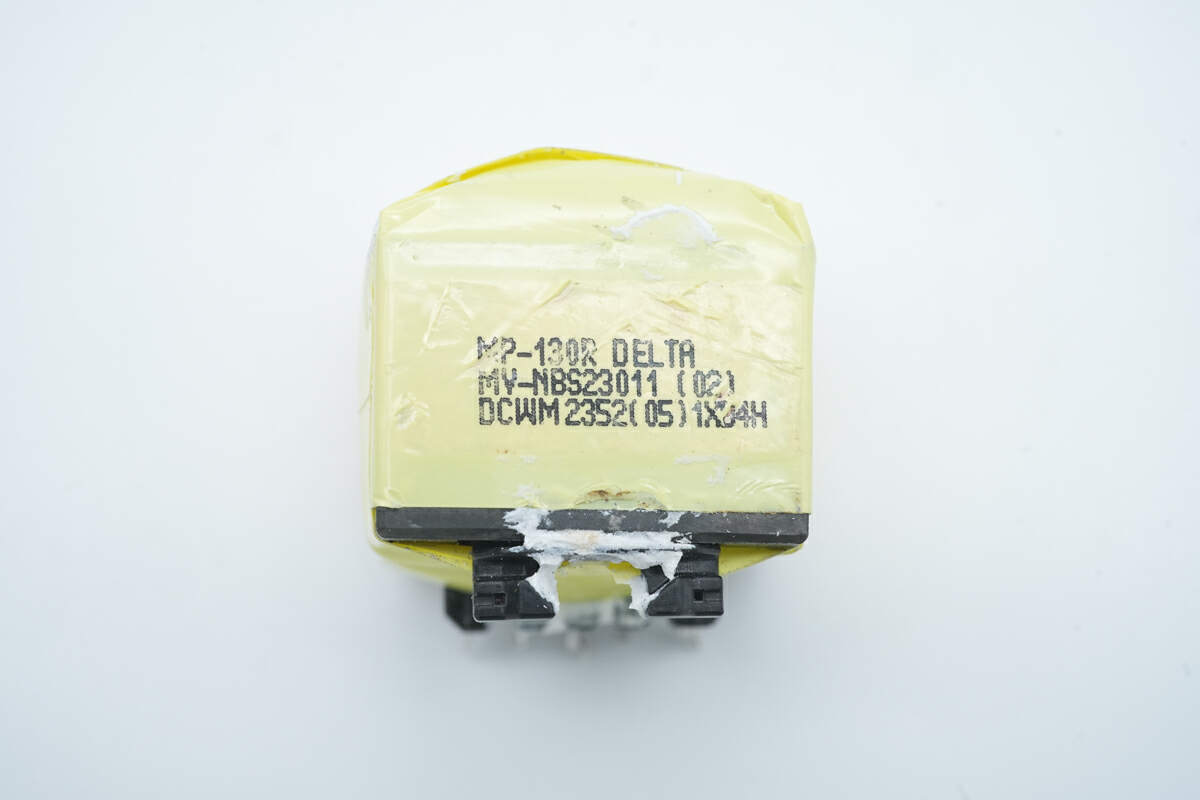
The magnetic core of the transformer is insulated by tape.
![Teardown of Lenovo 100W GaN Charger for Laptops (ADL100UDGC3A)-Chargerlab](https://www.chargerlab.com/wp-content/uploads/2024/07/2024072902225392.jpeg)
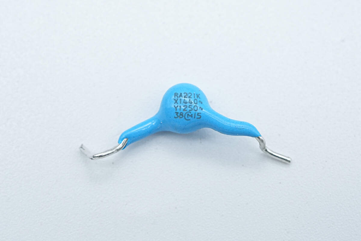
This is the blue Y capacitor.
![Teardown of Lenovo 100W GaN Charger for Laptops (ADL100UDGC3A)-Chargerlab](https://www.chargerlab.com/wp-content/uploads/2024/07/2024072902225814.jpeg)
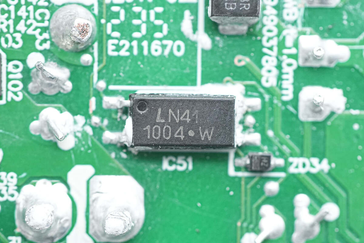
The optocoupler from LITEON is used for output voltage feedback regulation. Model is LTV1004.
![Teardown of Lenovo 100W GaN Charger for Laptops (ADL100UDGC3A)-Chargerlab](https://www.chargerlab.com/wp-content/uploads/2024/07/2024072902230132.jpeg)
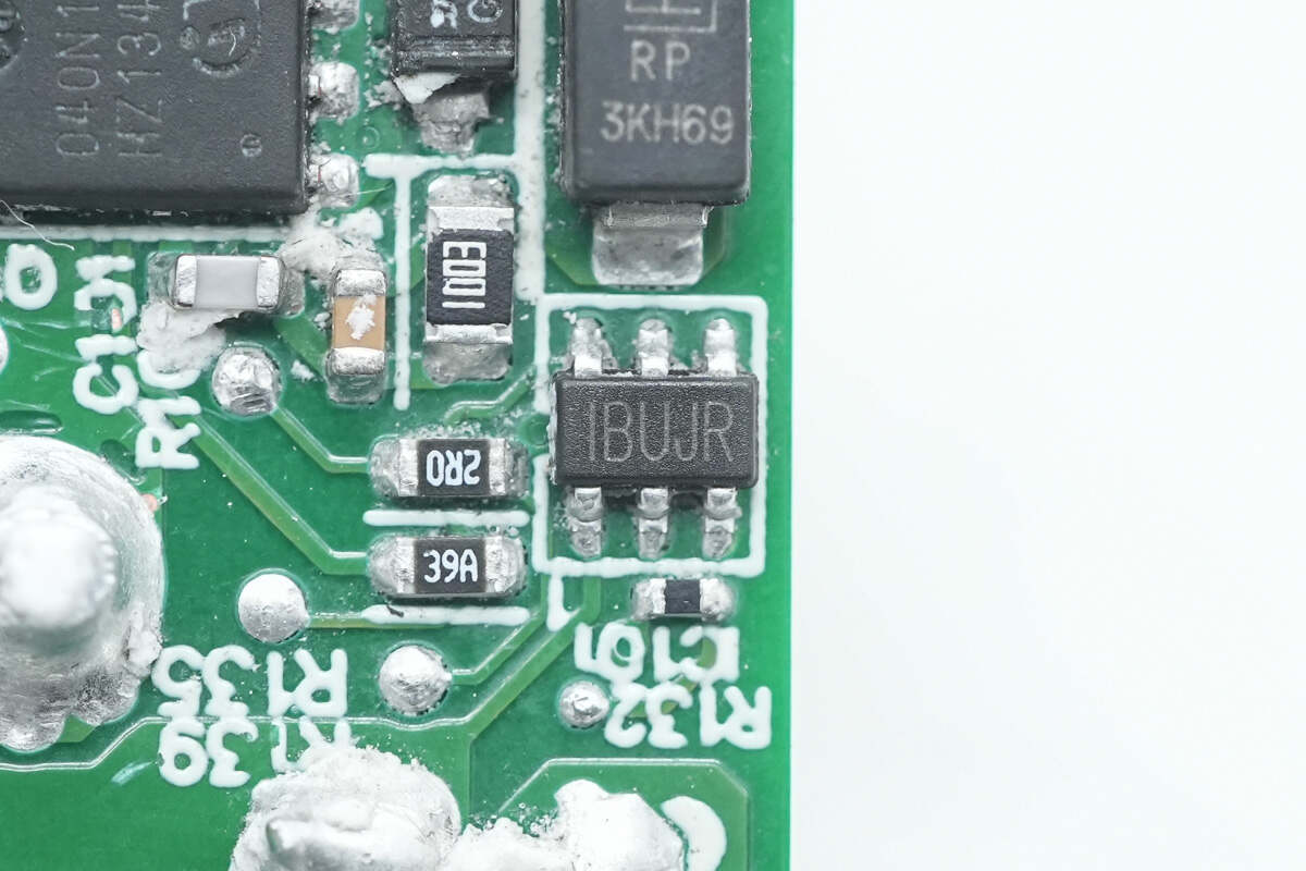
The synchronous rectifier controller marked with IBUJR is from MPS and adopts TSOT23-6 package. It supports DCM, CCM, QR, ZVS, ACF (active clamp flyback), and HFB (hybrid-flyback). And its operating frequency can reach 1MHz, and supports synchronous rectifier GaN FET. Model is MP6951.
![Teardown of Lenovo 100W GaN Charger for Laptops (ADL100UDGC3A)-Chargerlab](https://www.chargerlab.com/wp-content/uploads/2024/07/2024072902225997.jpeg)
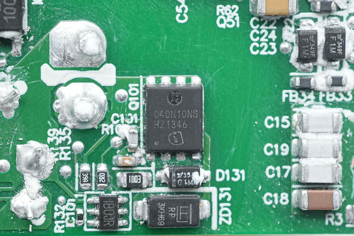
The synchronous rectifier is from Infineon and adopts PG-TDSON-8 package. Model is BSC040N10NS5. 100V 4mΩ.
![Teardown of Lenovo 100W GaN Charger for Laptops (ADL100UDGC3A)-Chargerlab](https://www.chargerlab.com/wp-content/uploads/2024/07/2024072902225137.jpeg)
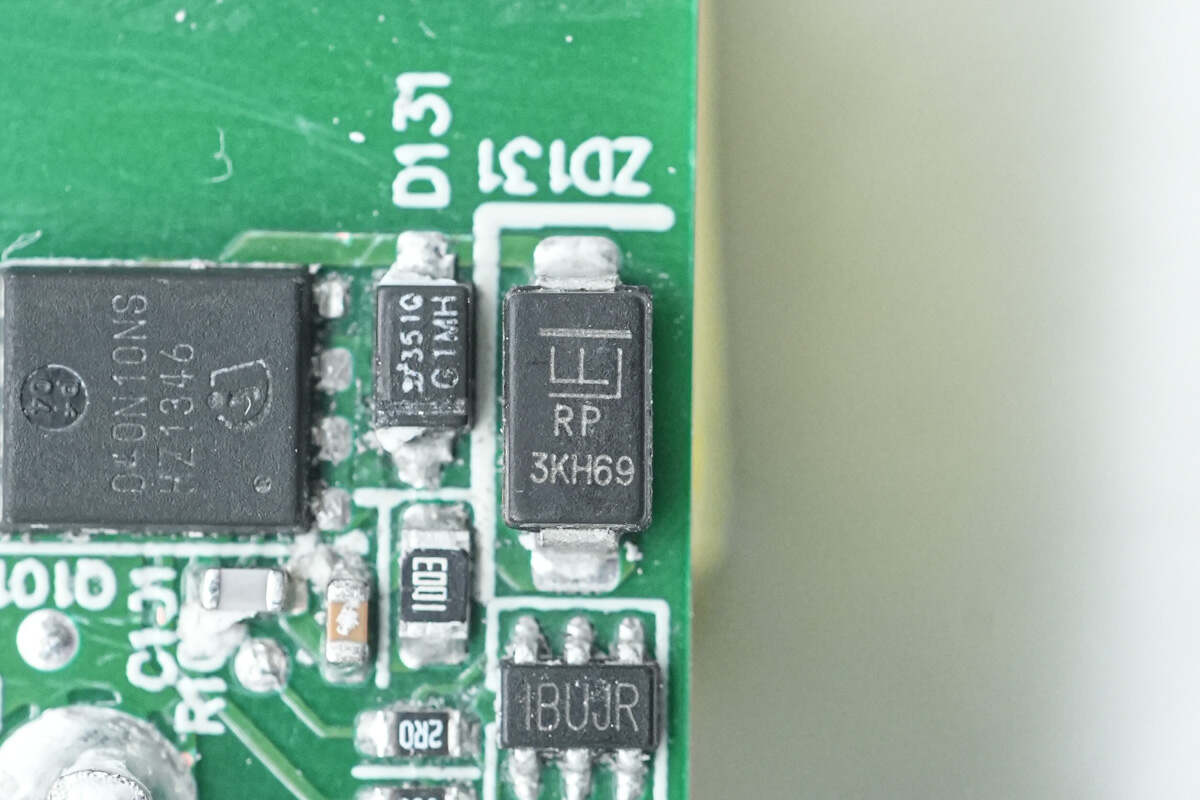
The TVS diode used to absorb surge overvoltage is from Littelfuse. Model is SMAJ70A.
![Teardown of Lenovo 100W GaN Charger for Laptops (ADL100UDGC3A)-Chargerlab](https://www.chargerlab.com/wp-content/uploads/2024/07/2024072902230032.jpeg)
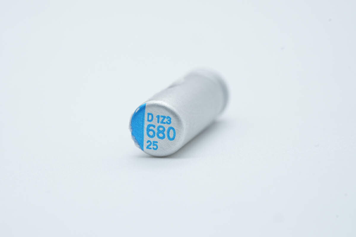
This is the solid capacitor for output filtering. 680μF 25V.
![Teardown of Lenovo 100W GaN Charger for Laptops (ADL100UDGC3A)-Chargerlab](https://www.chargerlab.com/wp-content/uploads/2024/07/2024072902225980.jpeg)
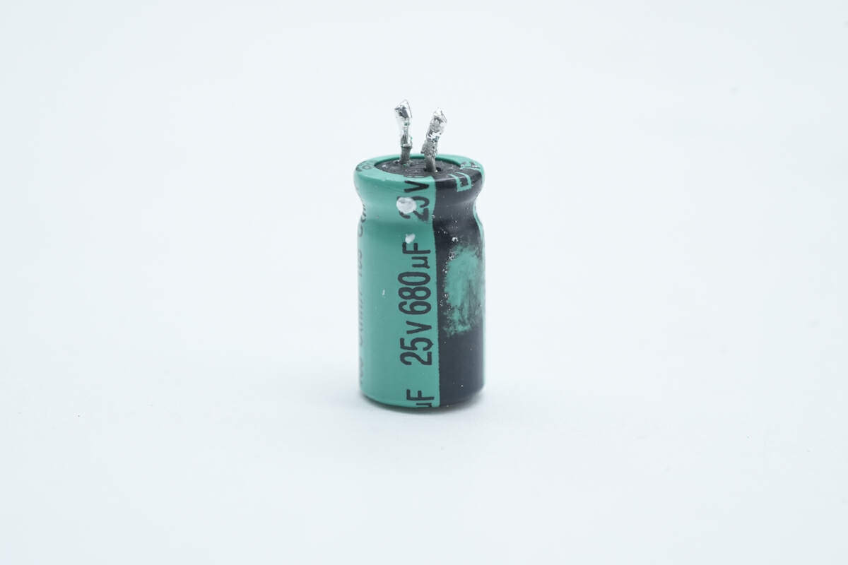
The electrolytic capacitor has the same specifications.
![Teardown of Lenovo 100W GaN Charger for Laptops (ADL100UDGC3A)-Chargerlab](https://www.chargerlab.com/wp-content/uploads/2024/07/2024072902225431.jpeg)
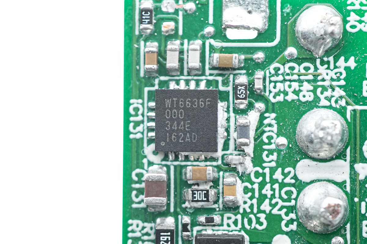
The protocol chip is from Weltrend. It supports USB PD3.0 and QC4+. It supports line loss compensation. Model is WT6636F.
![Teardown of Lenovo 100W GaN Charger for Laptops (ADL100UDGC3A)-Chargerlab](https://www.chargerlab.com/wp-content/uploads/2024/07/2024072902225910.jpeg)
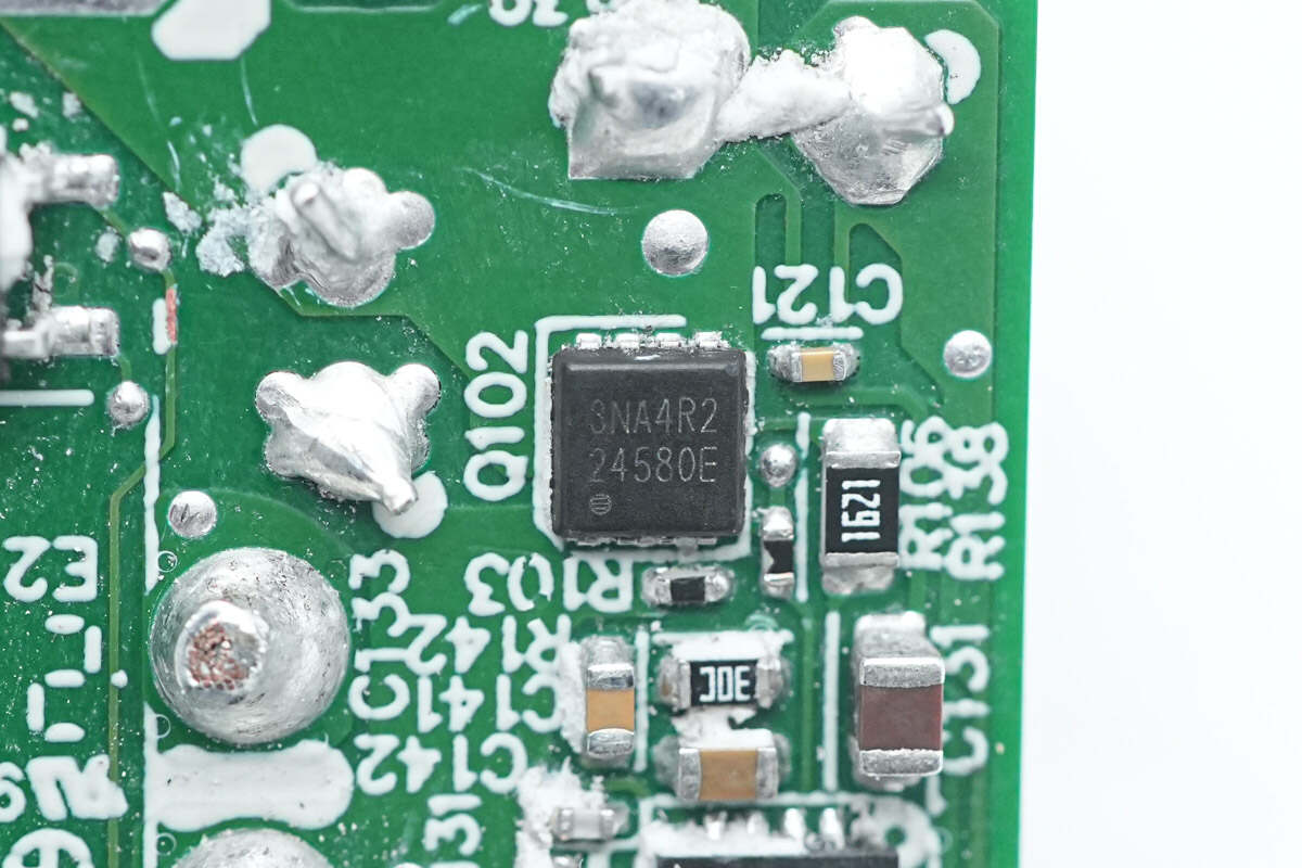
The VBUS MOSFET is from APEC and adopts PMPAK3*3 package. Model is AP3NA4R2YT. 30V 4.2mΩ.
![Teardown of Lenovo 100W GaN Charger for Laptops (ADL100UDGC3A)-Chargerlab](https://www.chargerlab.com/wp-content/uploads/2024/07/2024072902230192.jpeg)
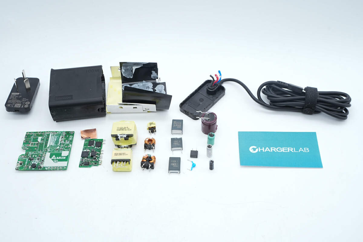
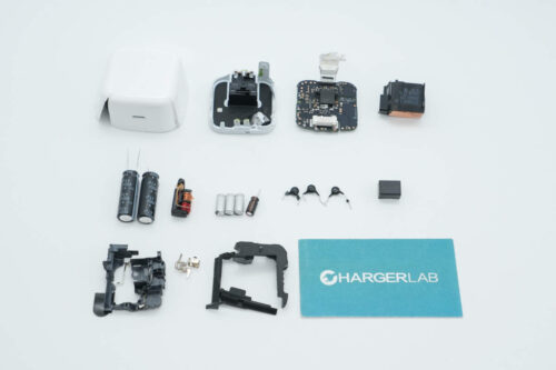
Well, those are all components of the Lenovo 100W GaN Charger.
Summary of ChargerLAB
![Teardown of Lenovo 100W GaN Charger for Laptops (ADL100UDGC3A)-Chargerlab](https://www.chargerlab.com/wp-content/uploads/2024/07/2024072902225771.png)
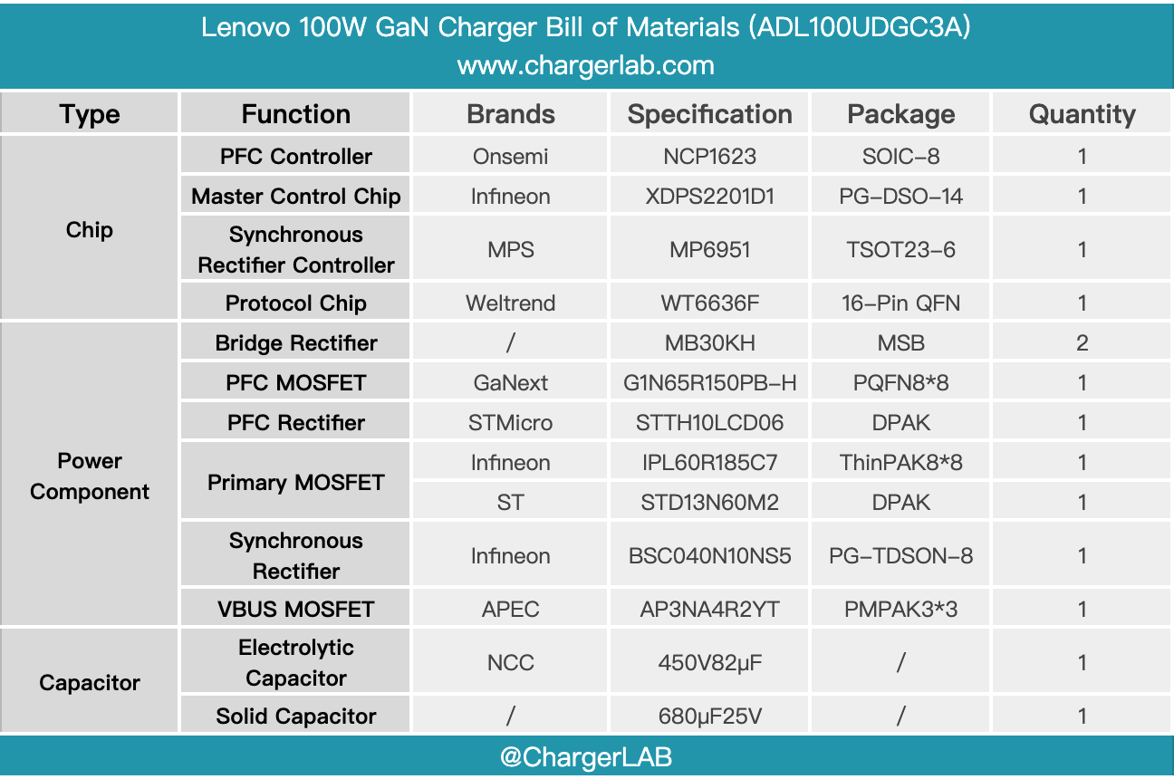
Here is the component list of the Lenovo 100W GaN Charger for your convenience.
It adopts a three-prong design and it comes with a 1.8-meter-long output cable, which can meet most usage scenarios.
After taking it apart, we found it adopts a PFC+HFB hybrid flyback topology, with a wide-range output voltage. The transformer and power component are filled with potting compound to enhance heat dissipation. And the PCBA module is also wrapped with aluminum sheets. It is optimized for high-power continuous output scenarios to improve performance.
Related Articles:
1. Teardown of Lenovo 170W AC Power Adapter (Square Connector)
2. Teardown of MOVESPEED 140W PD3.1 4-in-1 Charger (YSFCG107-140Y)
3. Teardown of LDNIO 140W GaN 6-in-1 Desktop Charger (A6140C)
All Comments (0)