Introduction
This time, ChargerLAB got a 140W GaN 6-in-1 desktop charger from LDNIO and it's only $40.99. Different from other chargers, it is equipped with a power cord and replaceable plugs, which can be used on the desktop or carried. It has three USB-C ports and three USB-A ports. It also comes with a display that can show the real-time charging power of each port. Let's take it apart and take a look at the internal components.
Product Appearance
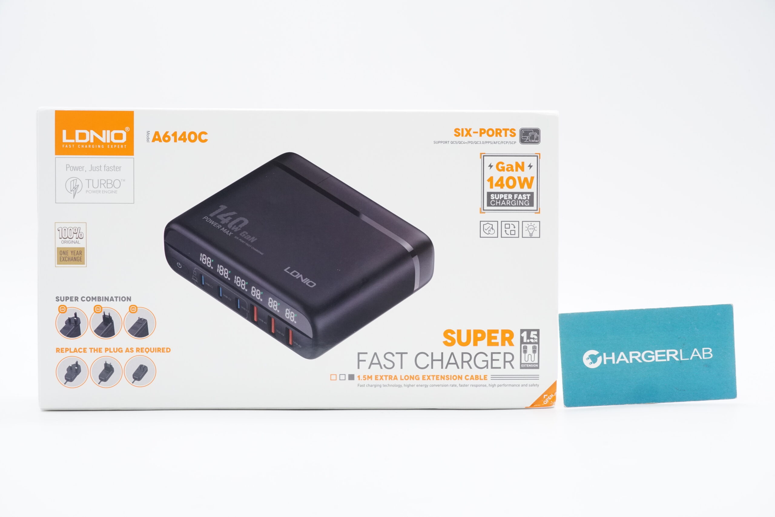
In addition to the LDNIO logo, product appearance, and GaN, the lower left corner also has the appearance of three different kinds of plugs on the front of the box.
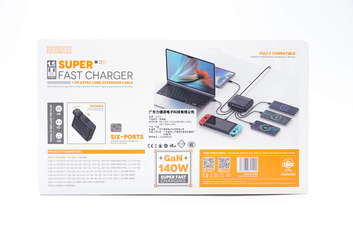
The back has two illustrations of how to replace the plugs and use the charger to charge six devices at the same time.
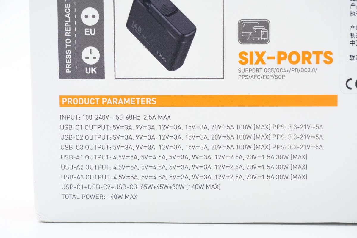
Specs info are printed on the lower left corner, we'll talk about later.
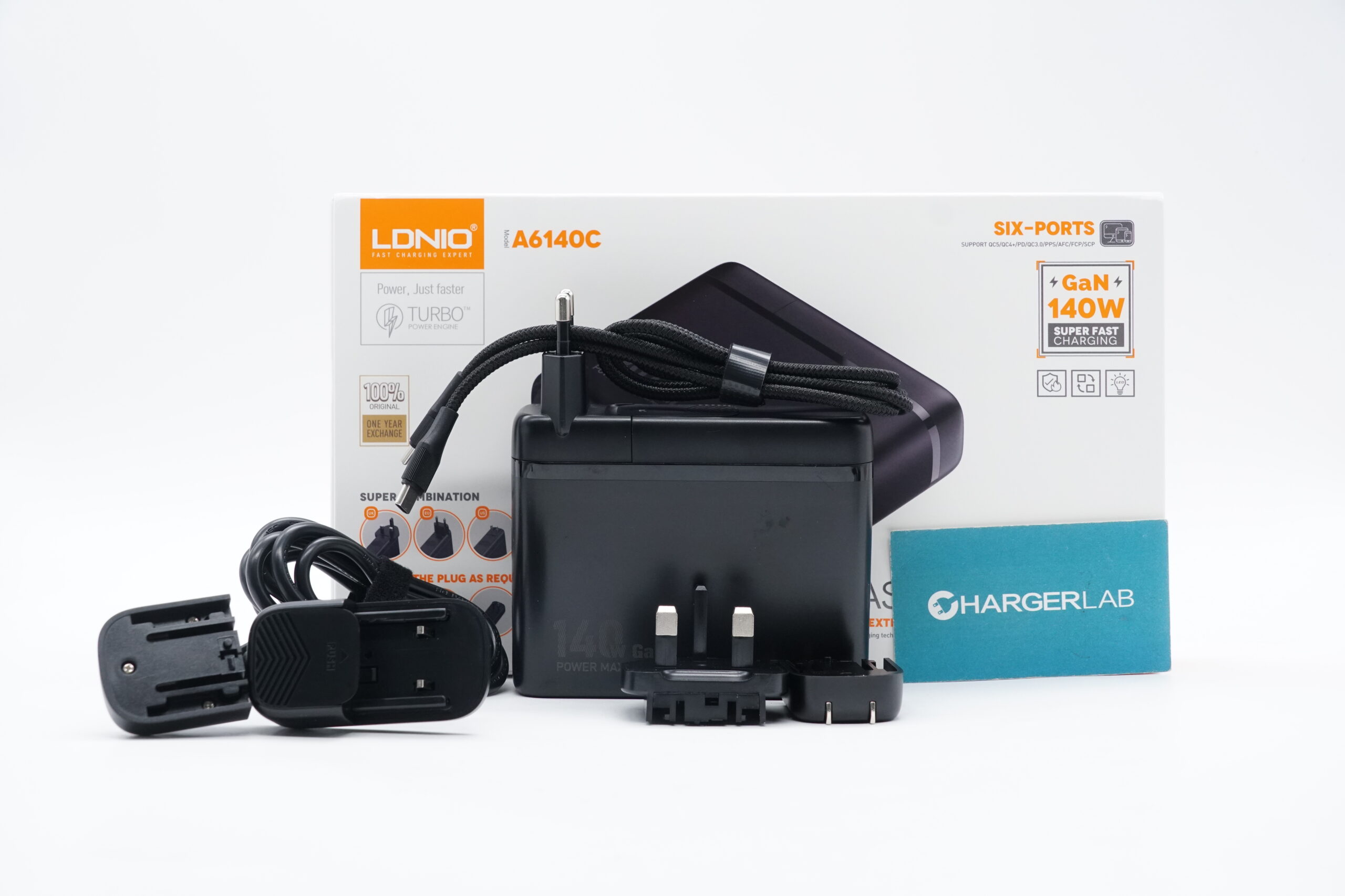
The box includes the charger, plugs, dual USB-C cable, and power cord.
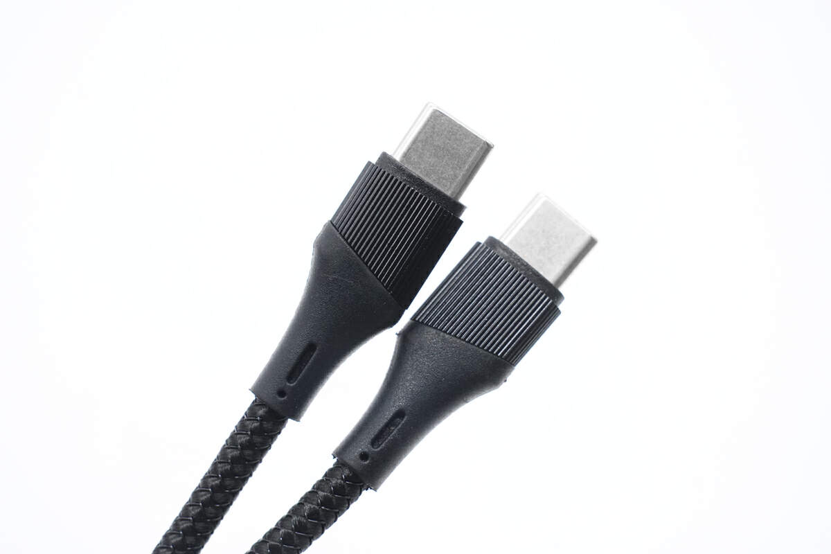
The dual USB-C cable adopts a braided design. The connector has an uneven surface for easy plugging and unplugging.

Hard plastic strings are added to the braiding to increase lifespan.
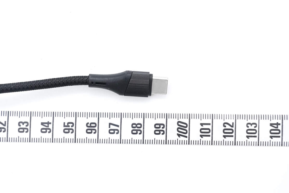
Its length is about 1 m (3' 3.37'').
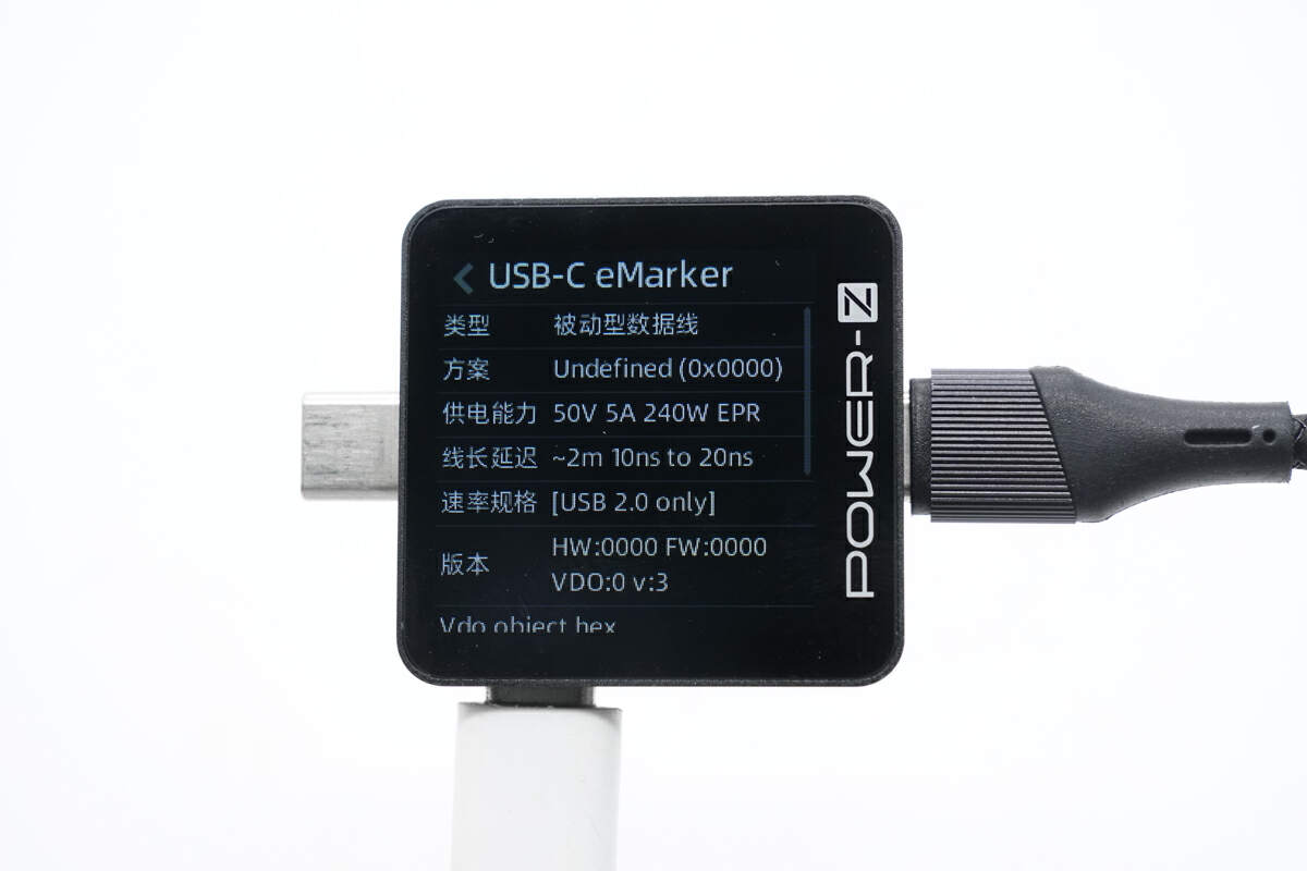
ChargerLAB POWER-Z KM003C shows that it is a PD3.1 cable and can support 240W of power transmission. It has an E-marker chip. And it only supports USB 2.0.
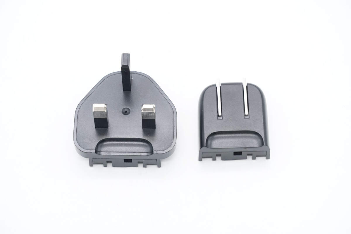
Here are the other two replaceable plugs, they also adopt grooves same as the power cord.
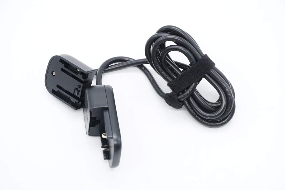
The power cord has clip fixed design. The plugs can be used on both the power cord and the charger.
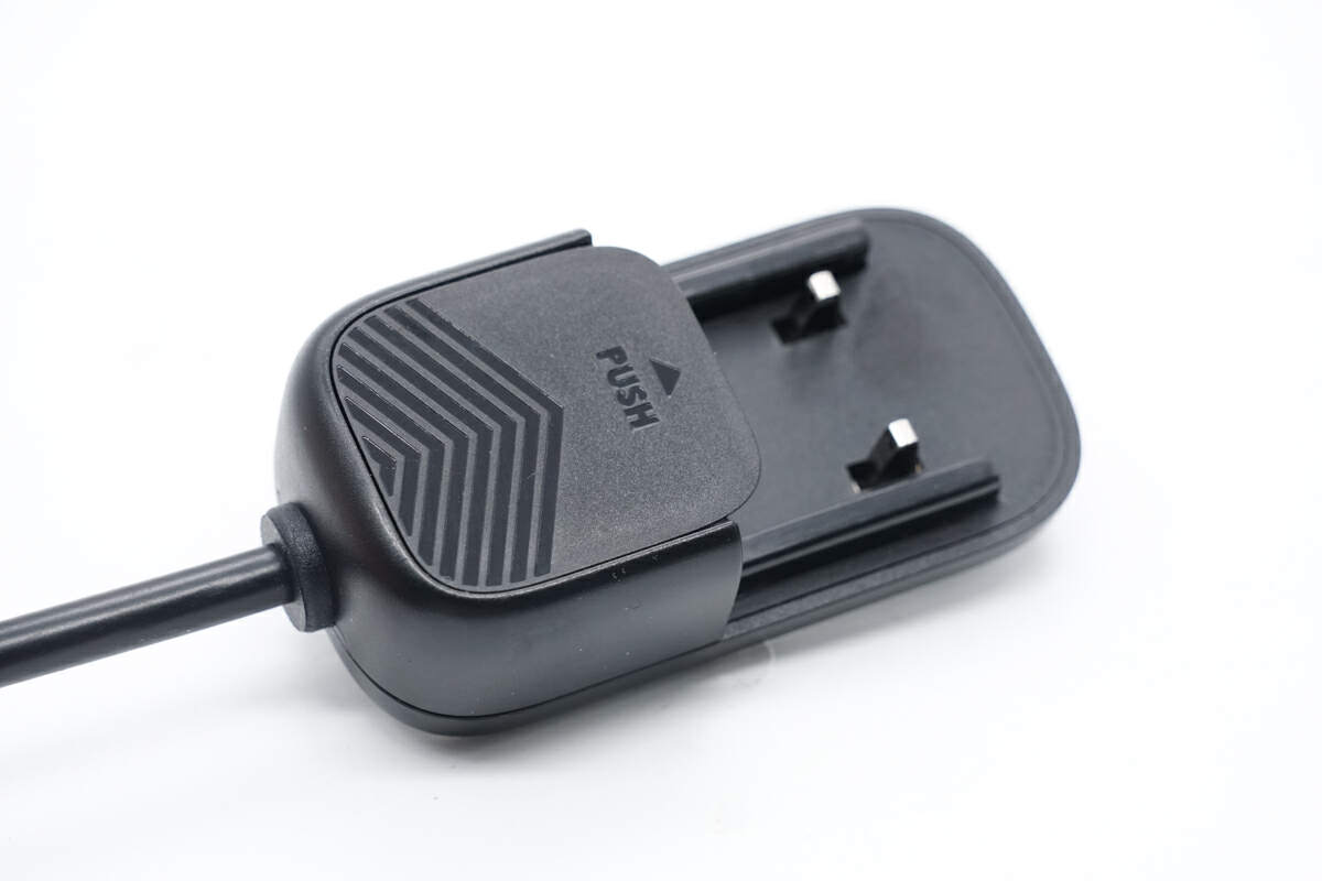
The input end has a slide button for disassembly.
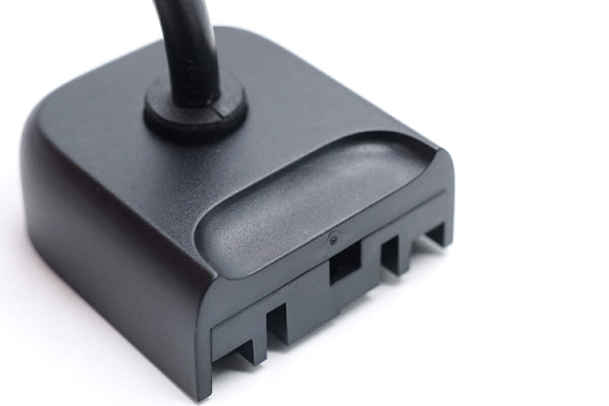
And the output end has grooves to separate the power cord from the charger.
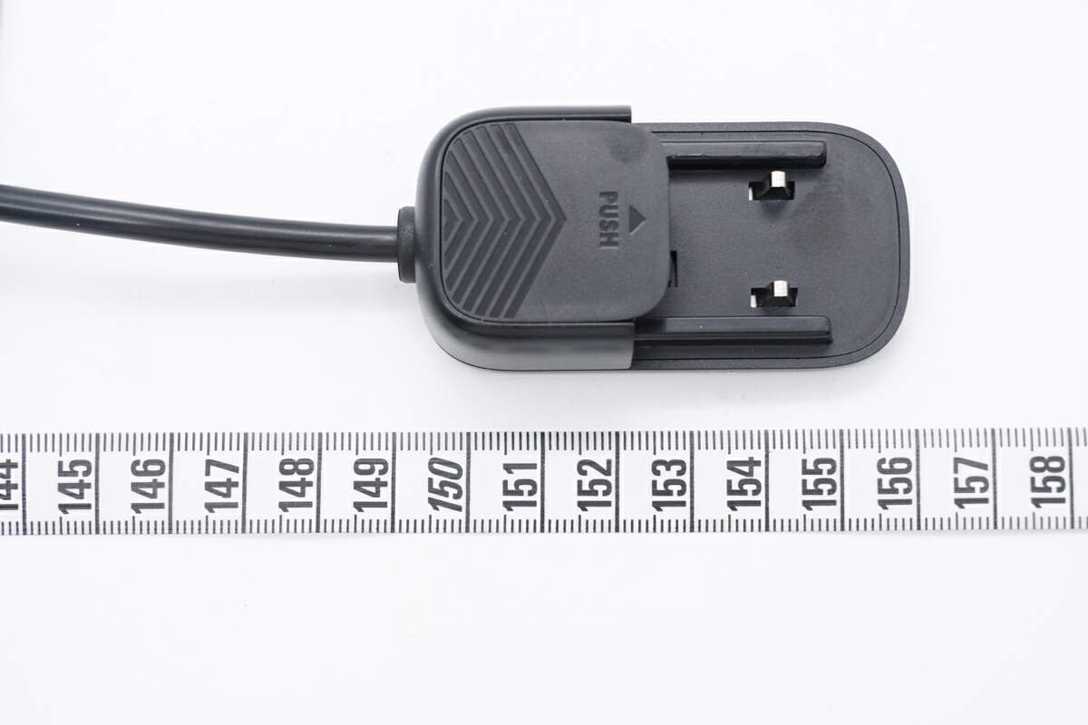
Its length is about 1.56 m (5' 1.42'').
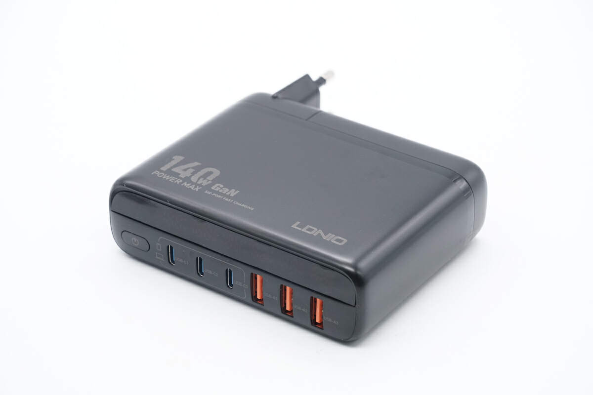
The case of the charger is made of black PC material with a matte finish.
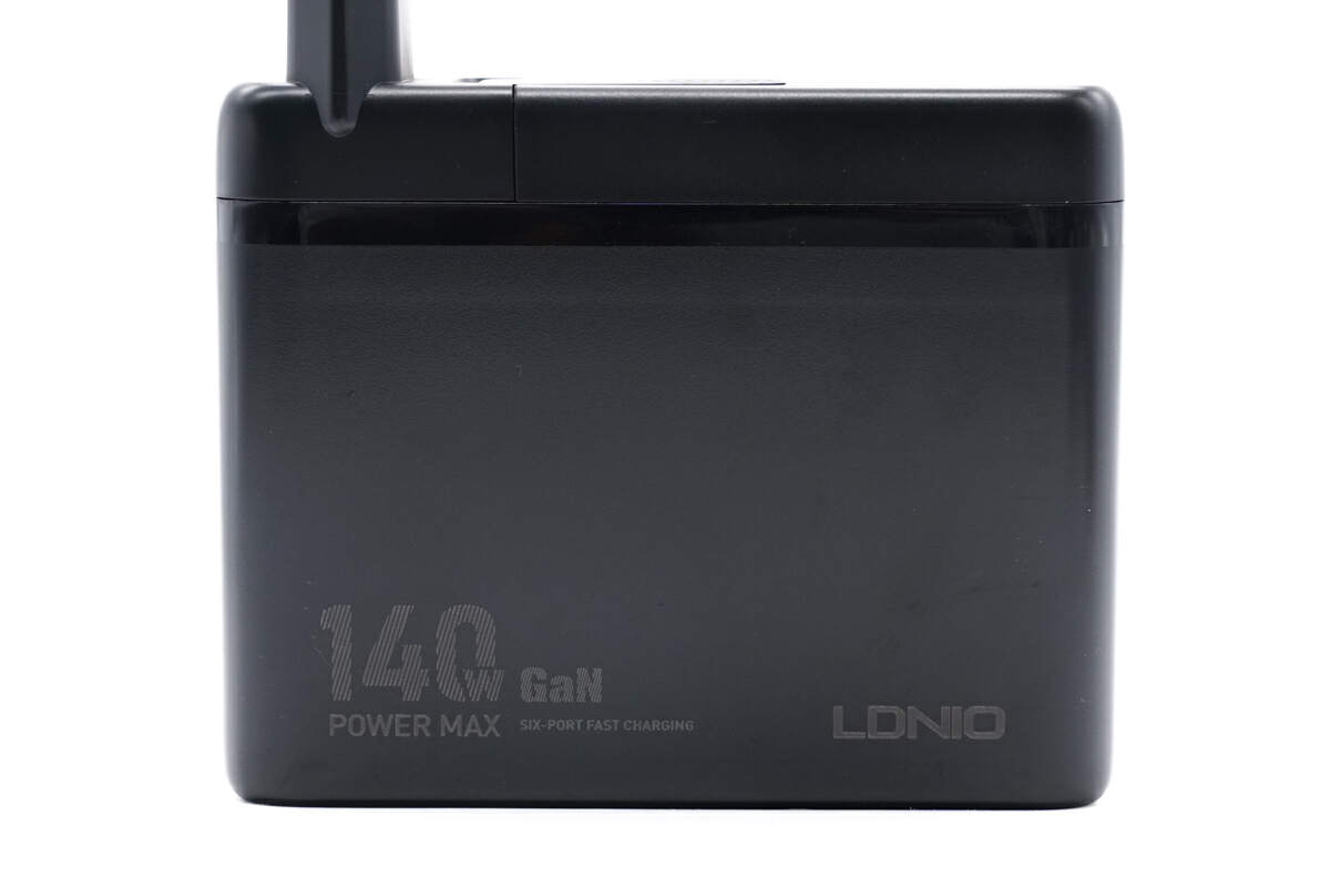
The LDNIO logo, 140W, and GaN are printed on the front.
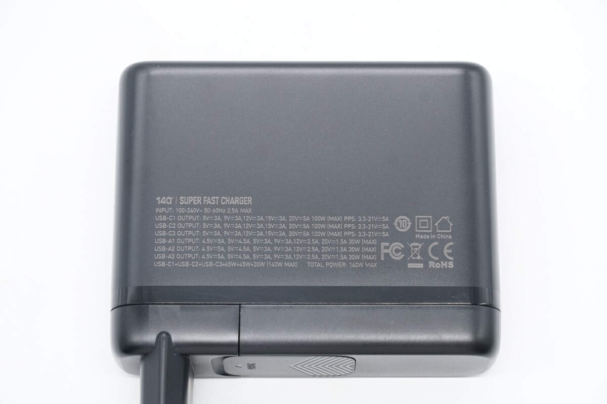
The specs info are also printed on the back of it.
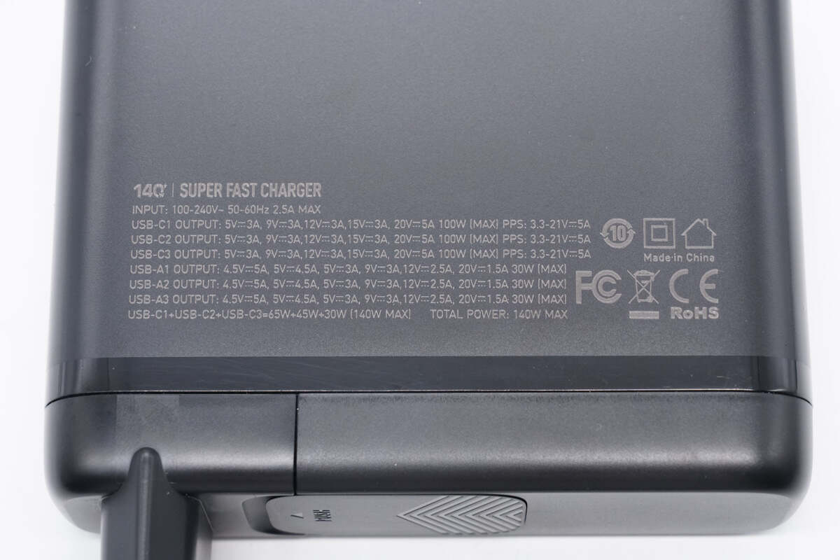
It can support input of 100-240V~ 50/60Hz 2.5A. The maximum charging power of the USB-C and USB-A ports are 100W and 30W, respectively. The power distribution is 65W+45W+30W.
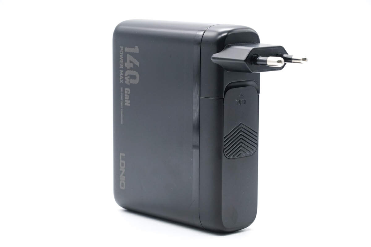
The EU plug is pre-installed on the charger.
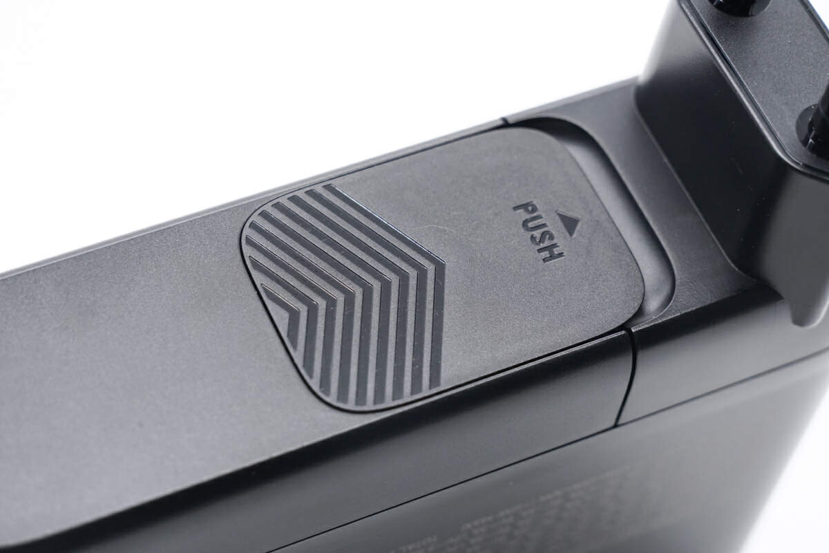
The input end has the same slide button as the power cord for a easy separation.
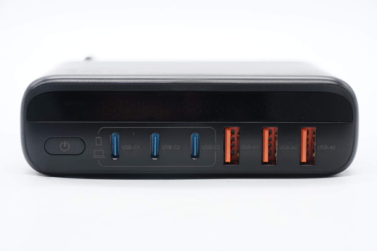
It has three blue USB-C ports and three orange ports. The display above the ports can show the real-time charging power of each port, like a mini version of POWER-Z KM003C.
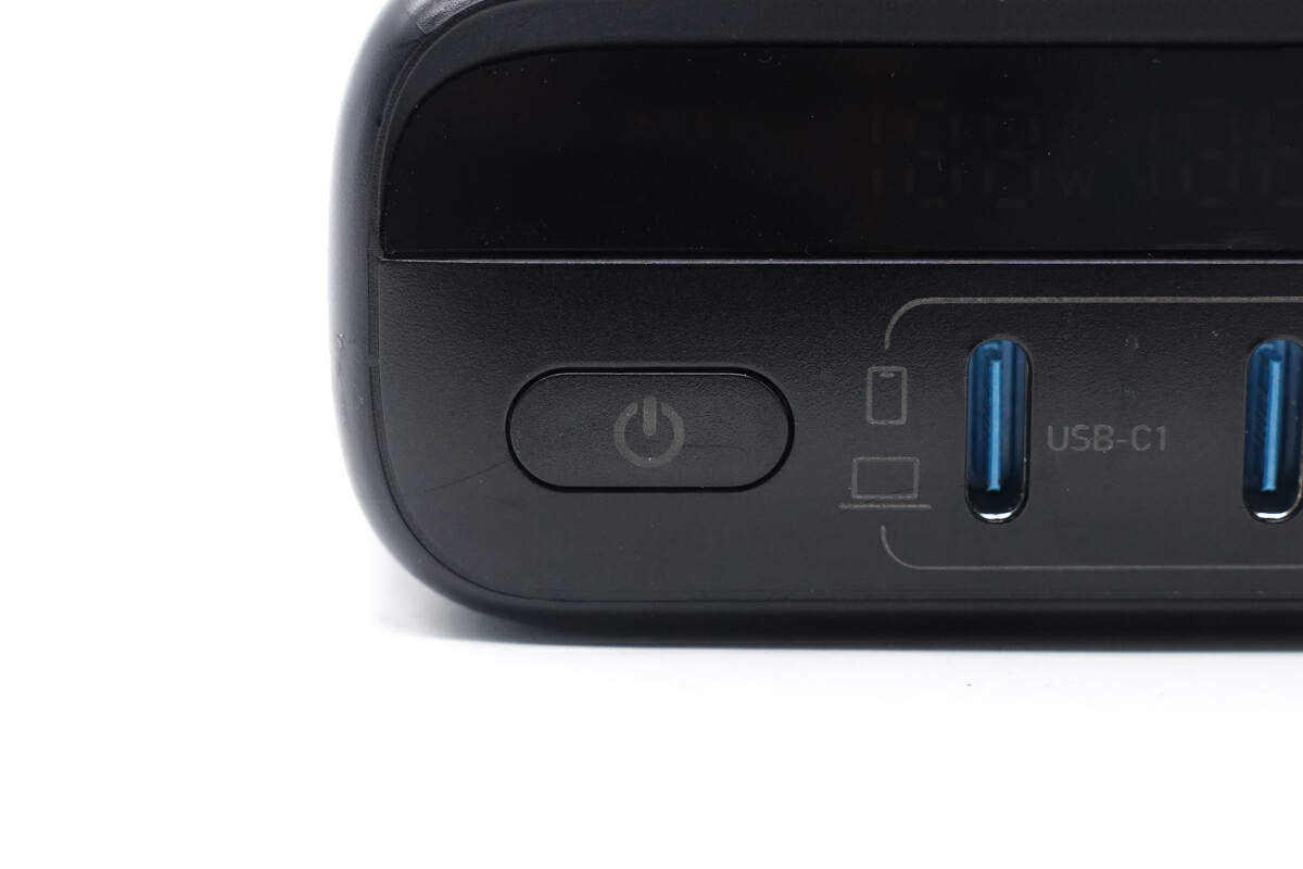
There is a power button in the lower left corner.
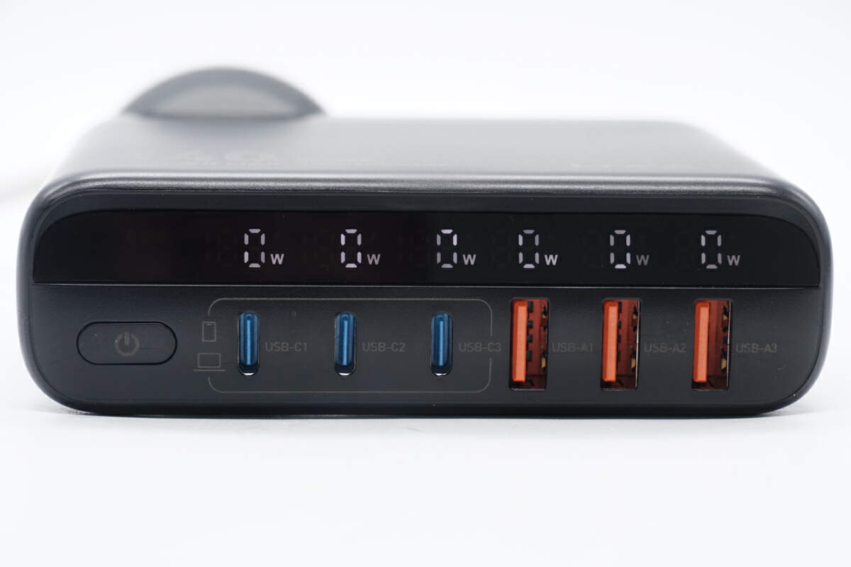
Pressing the button can wake up the display.
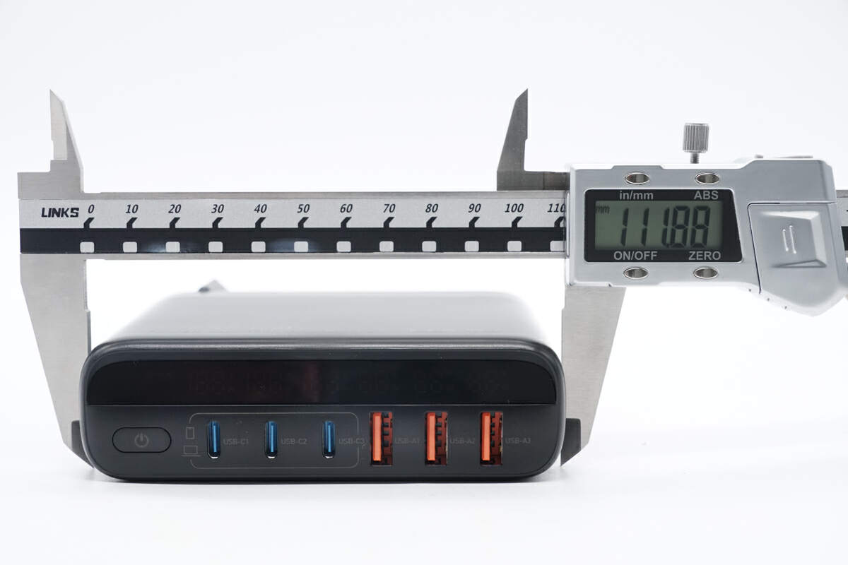
The length is about 112 mm (4.41 inches).
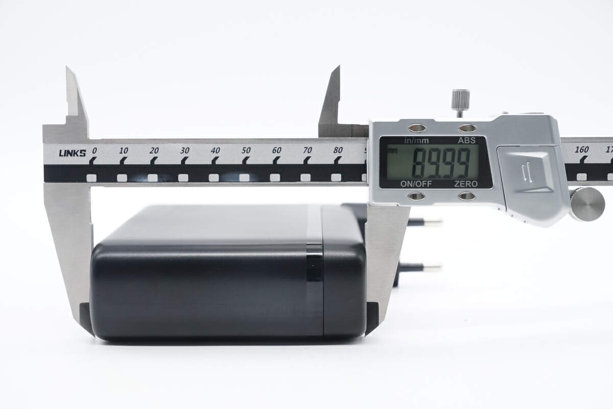
The height is about 90 mm (3.54 inches).
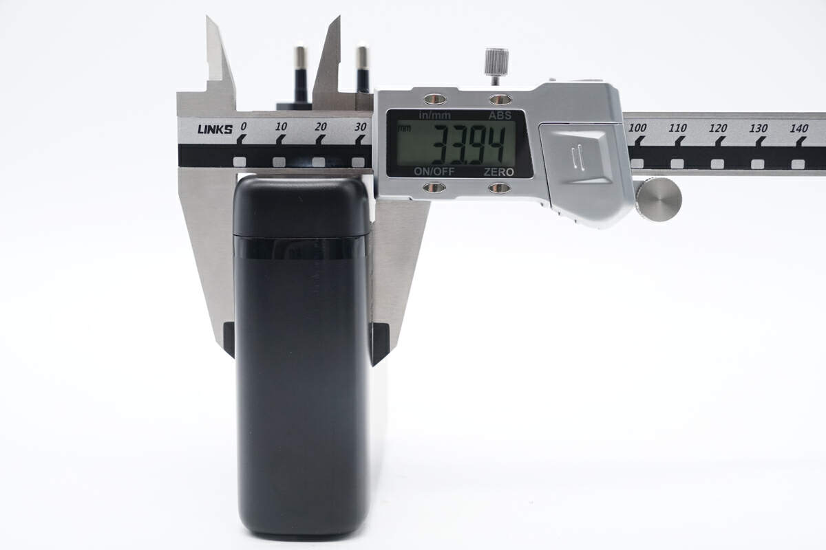
The width is about 34 mm (1.34 inches).
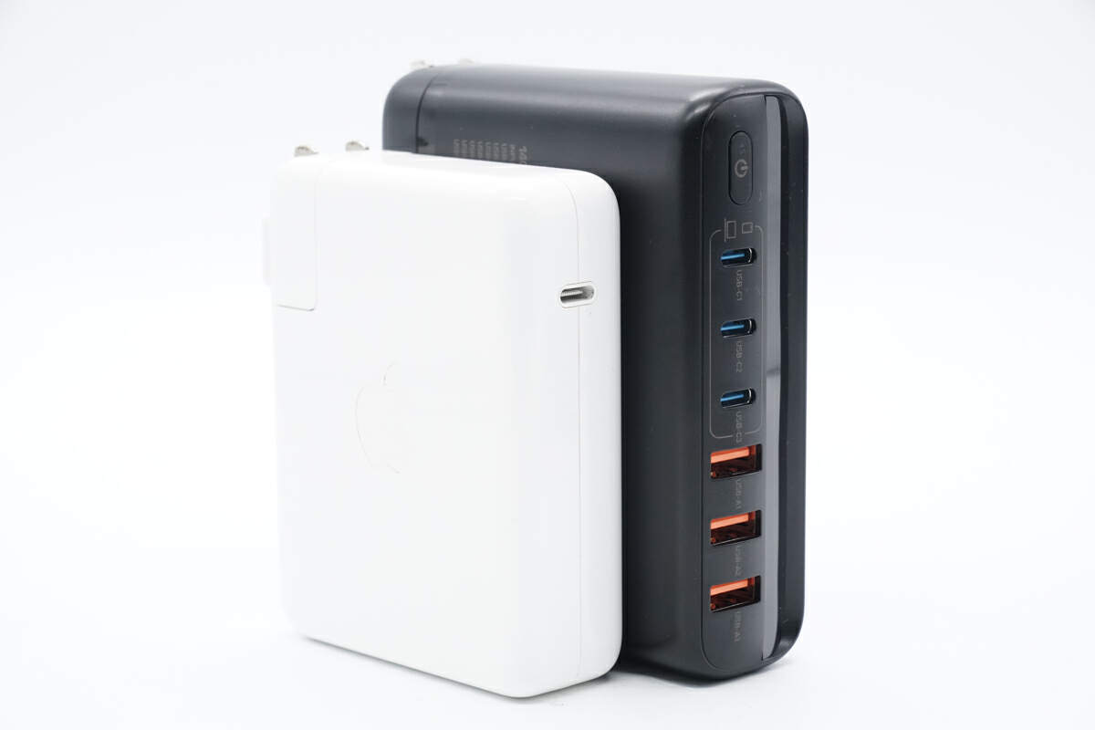
It is bigger than the Apple 140W GaN charger. As a multi-port charger, this is acceptable.
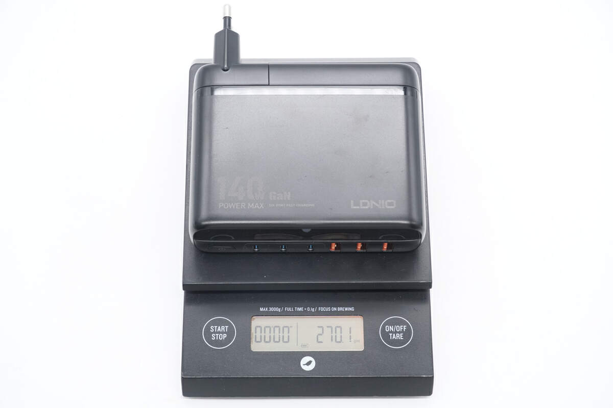
And the weight is about 270 g (9.52 oz).
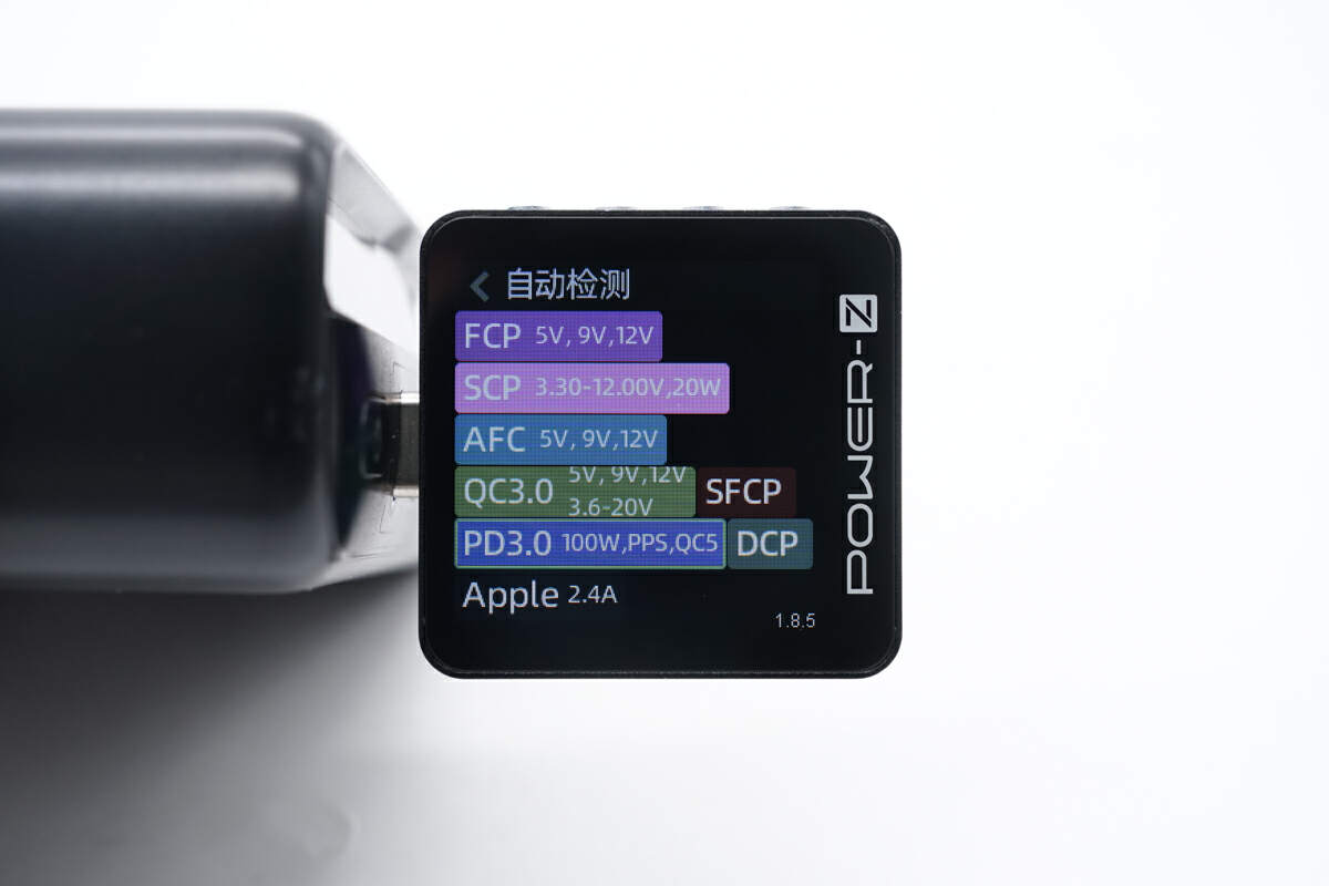
The ChargerLAB POWER-Z KM003C shows that the USB-C1 supports FCP, SCP, AFC, QC3.0/5, SFCP, PD3.0, PPS, DCP, and Apple 2.4A protocols.
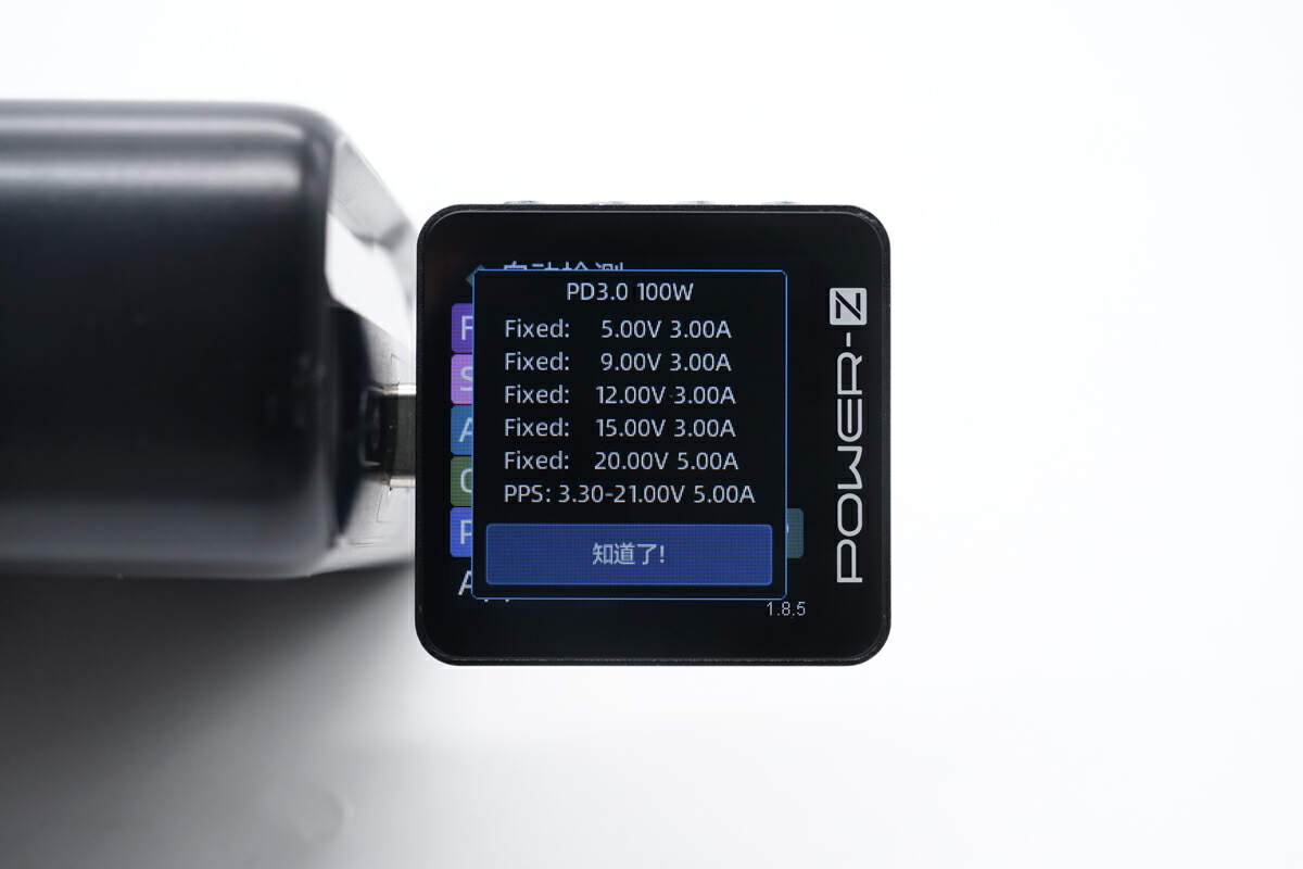
And the USB-C1 has five fixed PDOs of 5V3A, 9V3A, 12V3A, 15V3A, and 20V5A, and a set of PPS, which is 3.3-21V5A.
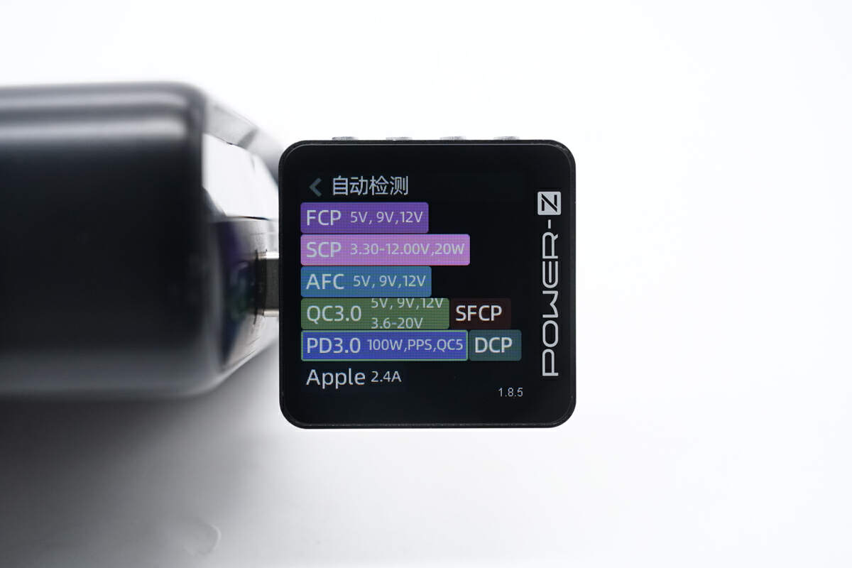
The supported protocols of USB-C2 are the same as the USB-C1.
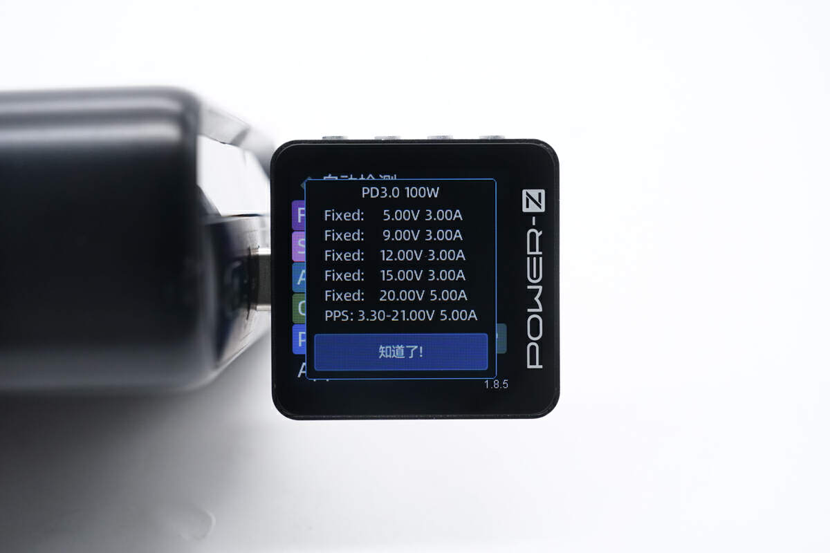
So are the PDOs.
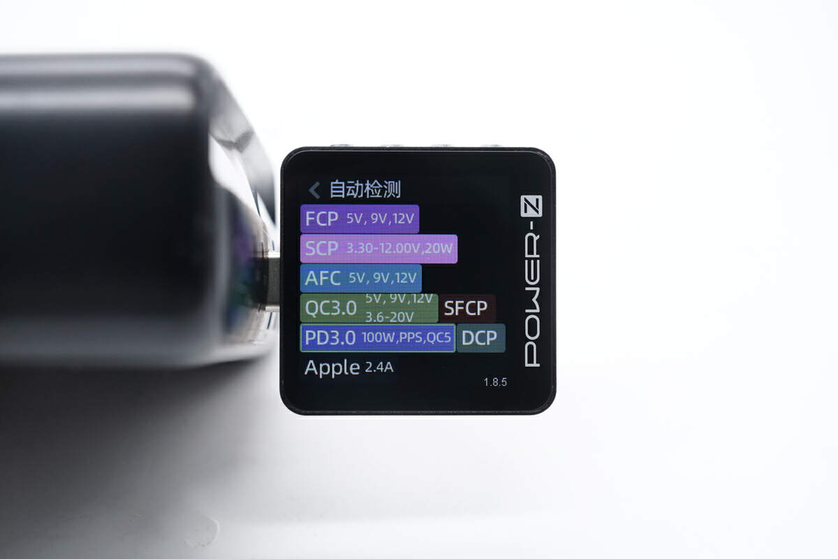
The supported protocols of USB-C3 are the same as the previous two ports.
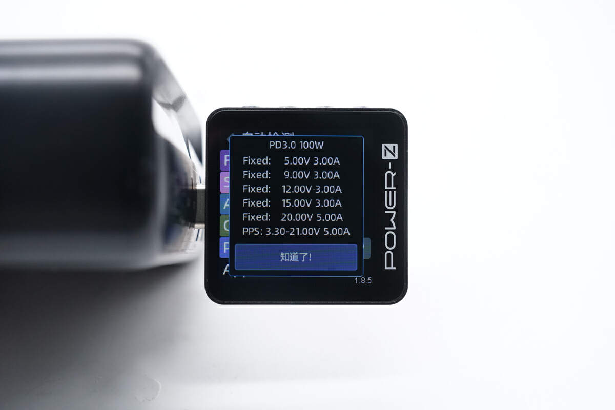
So are the PDOs. So the performance of these three USB-C ports is the same.
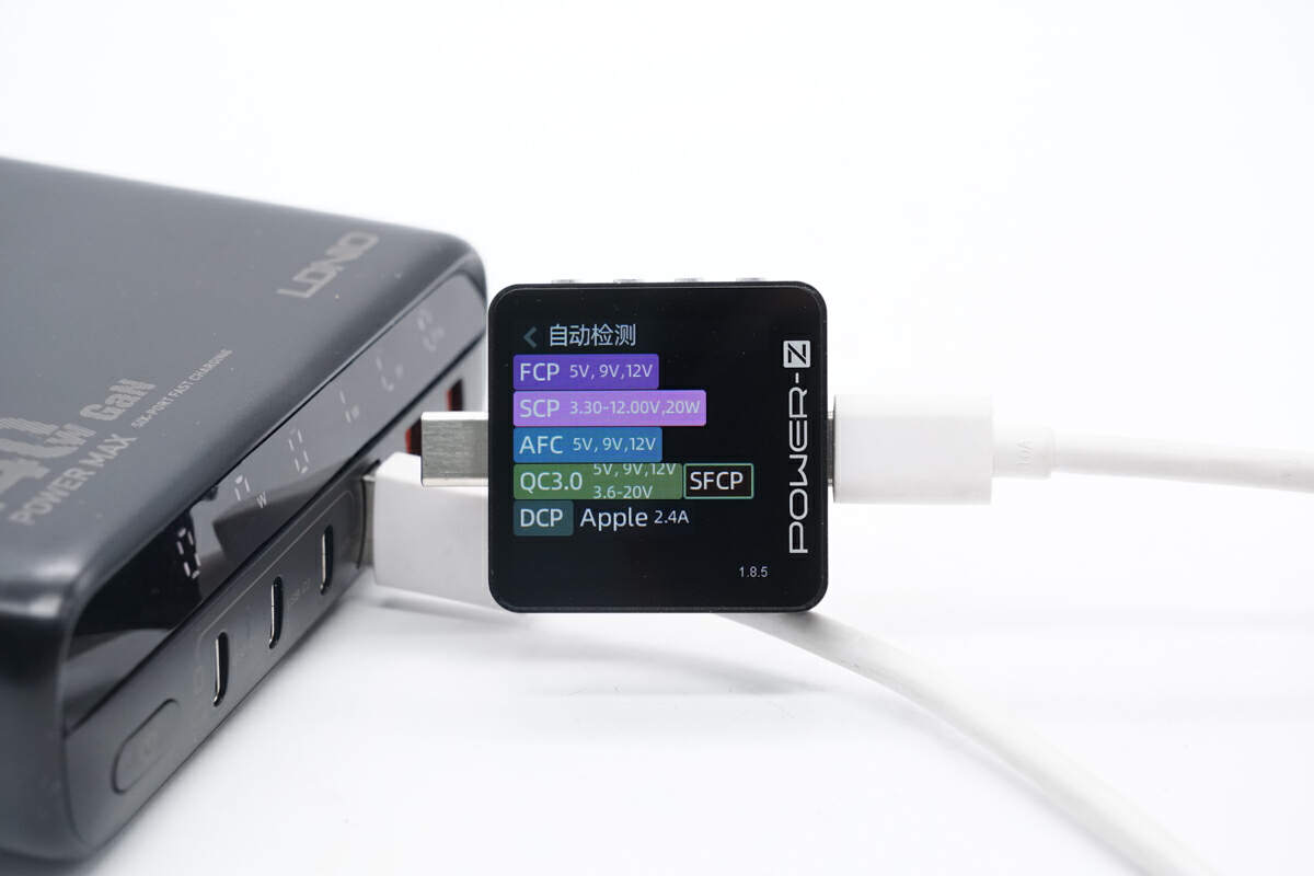
The USB-A1 supports FCP, SCP, AFC, QC3.0, SFCP, DCP, and Apple 2.4A protocols.
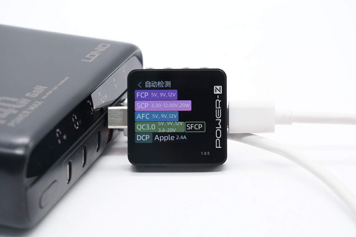
The supported protocols of USB-A2 are the same as the USB-A1.
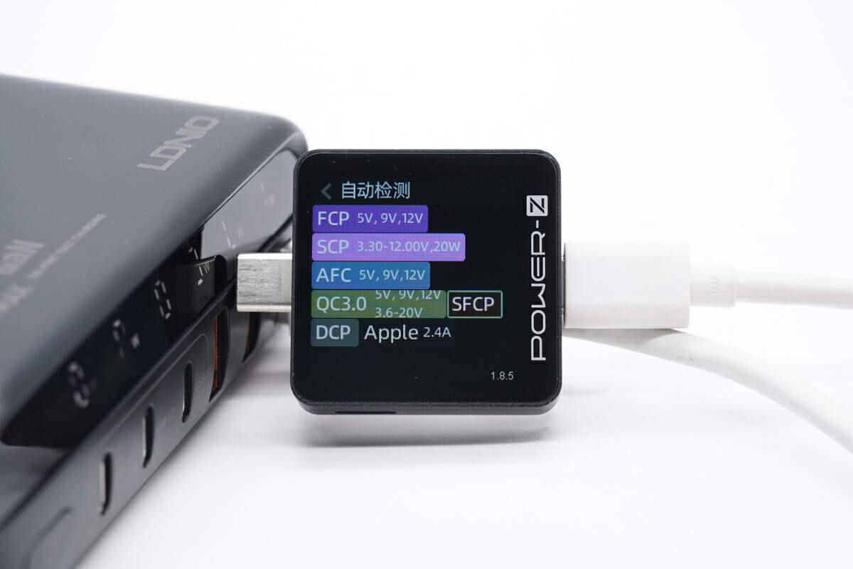
The supported protocols of USB-A3 are the same as the previous two USB-A ports.
Teardown
Next, we will take it apart.
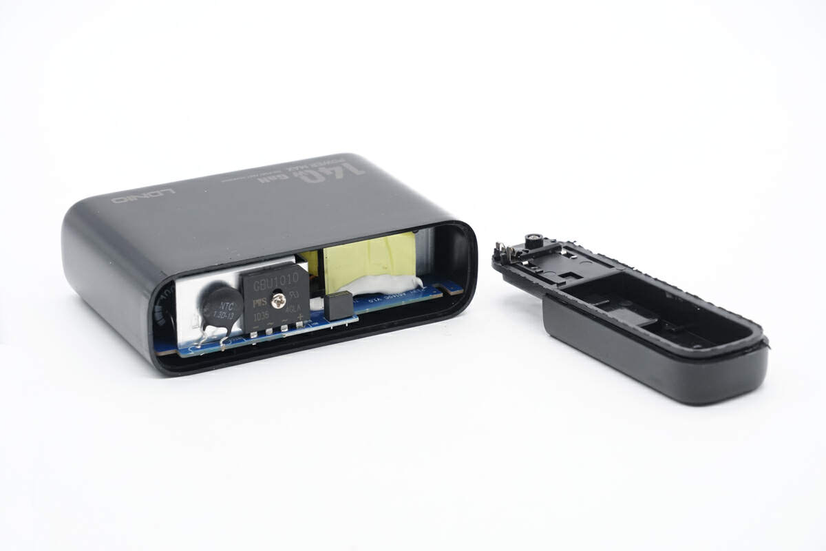
Remove the upper cover along the grooves.
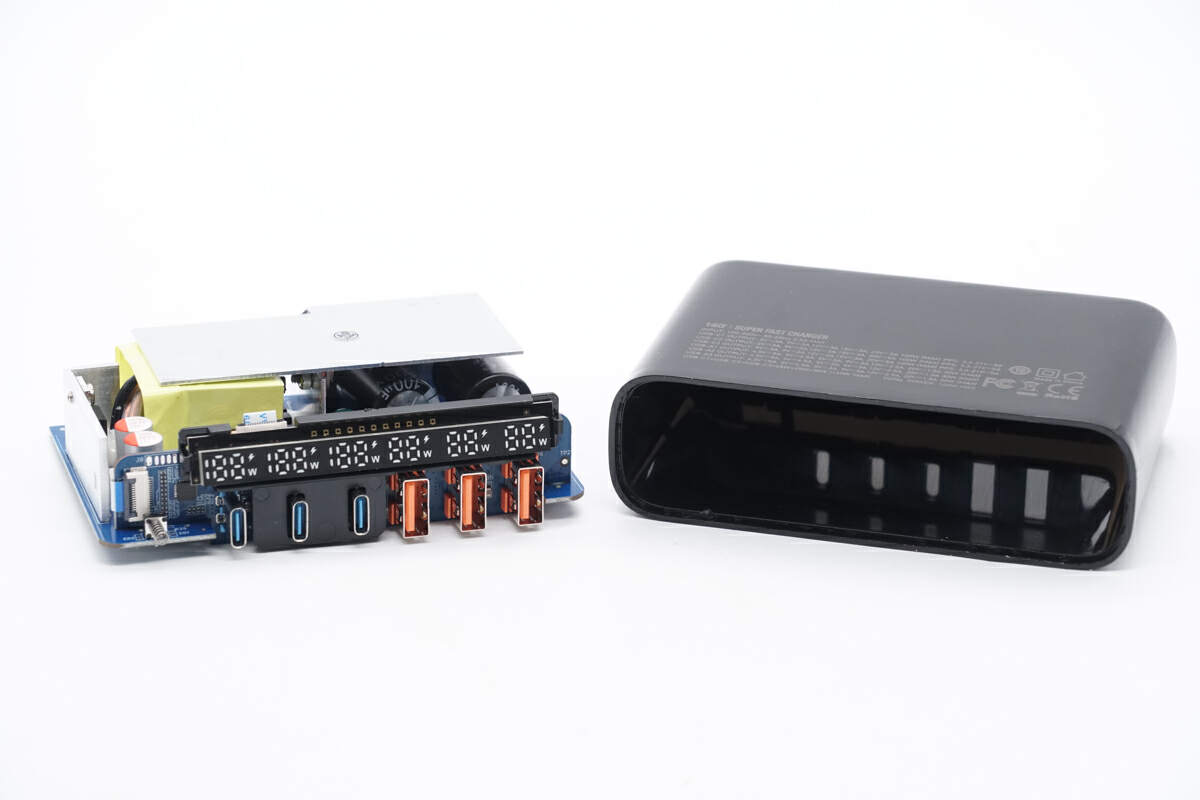
Take out the PCBA module from the case.
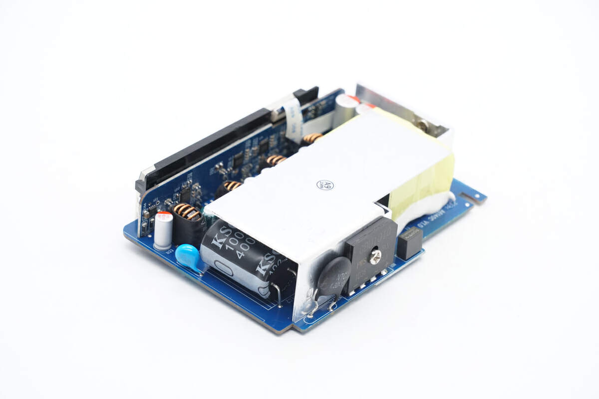
There are heat sinks on the PCBA module.
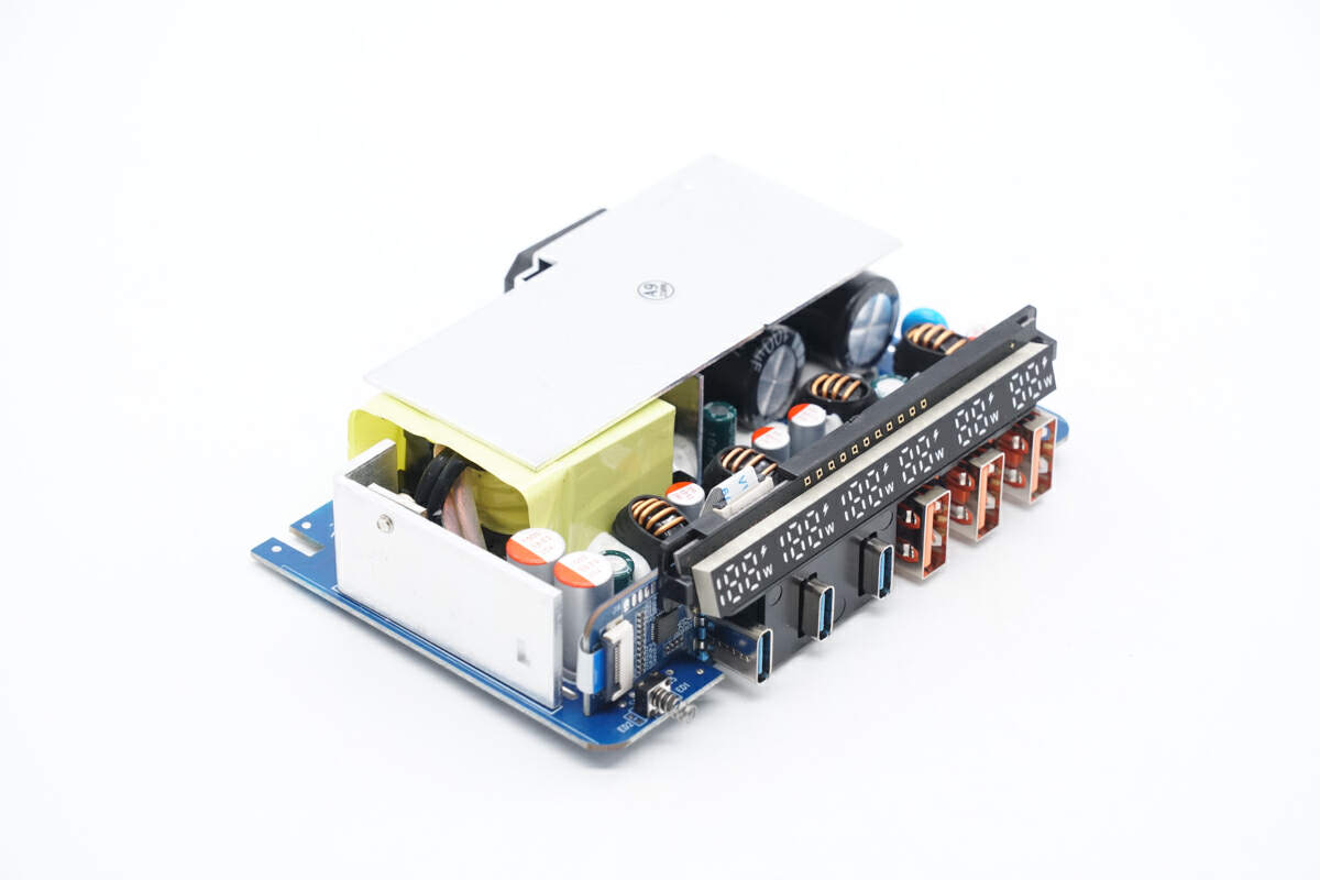
And the display and sockets are on the small PCB at the output end.
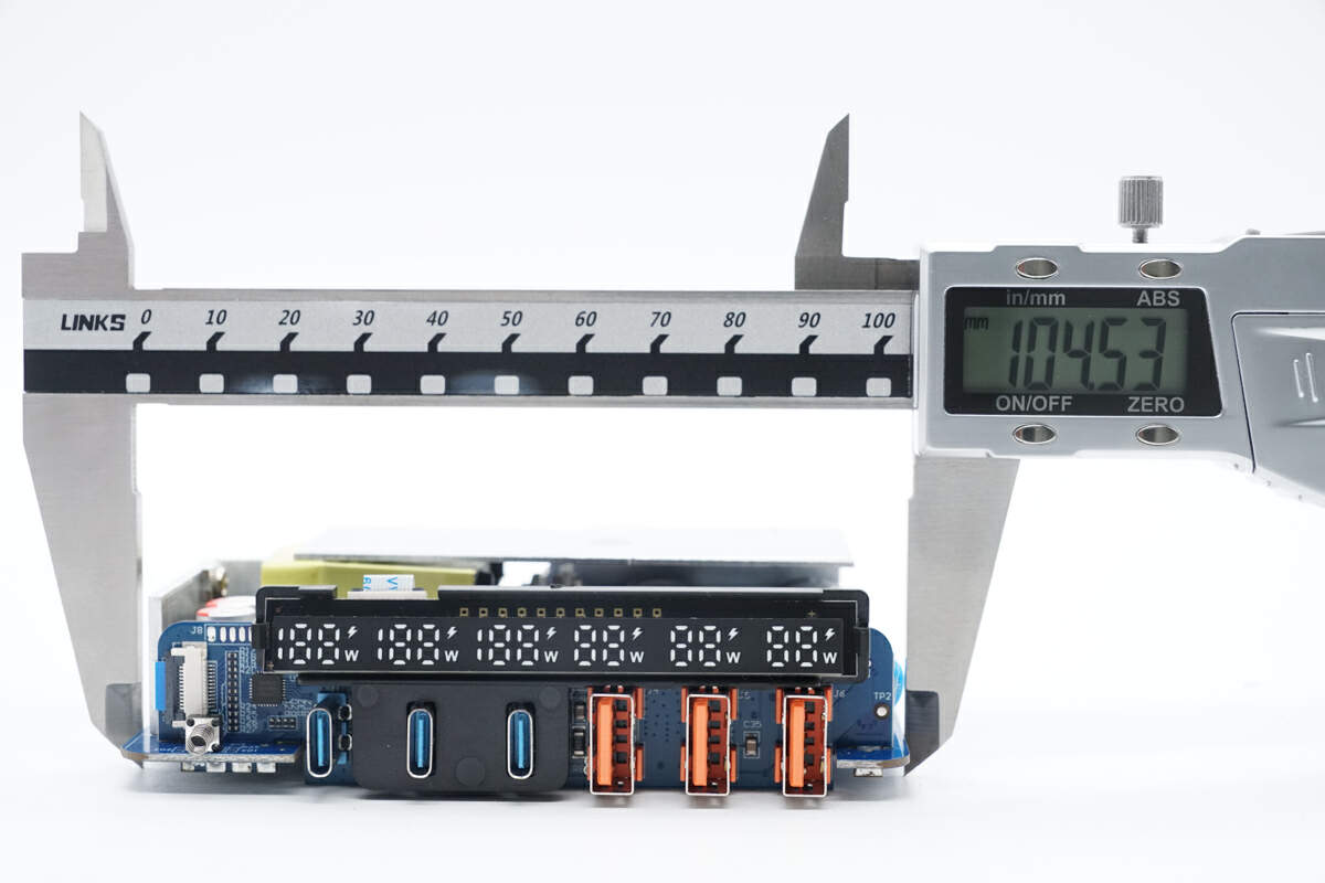
The length of the PCBA module is about 105 mm (4.13 inches).
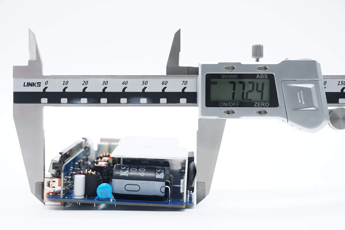
The width is about 77 mm (3.03 inches).
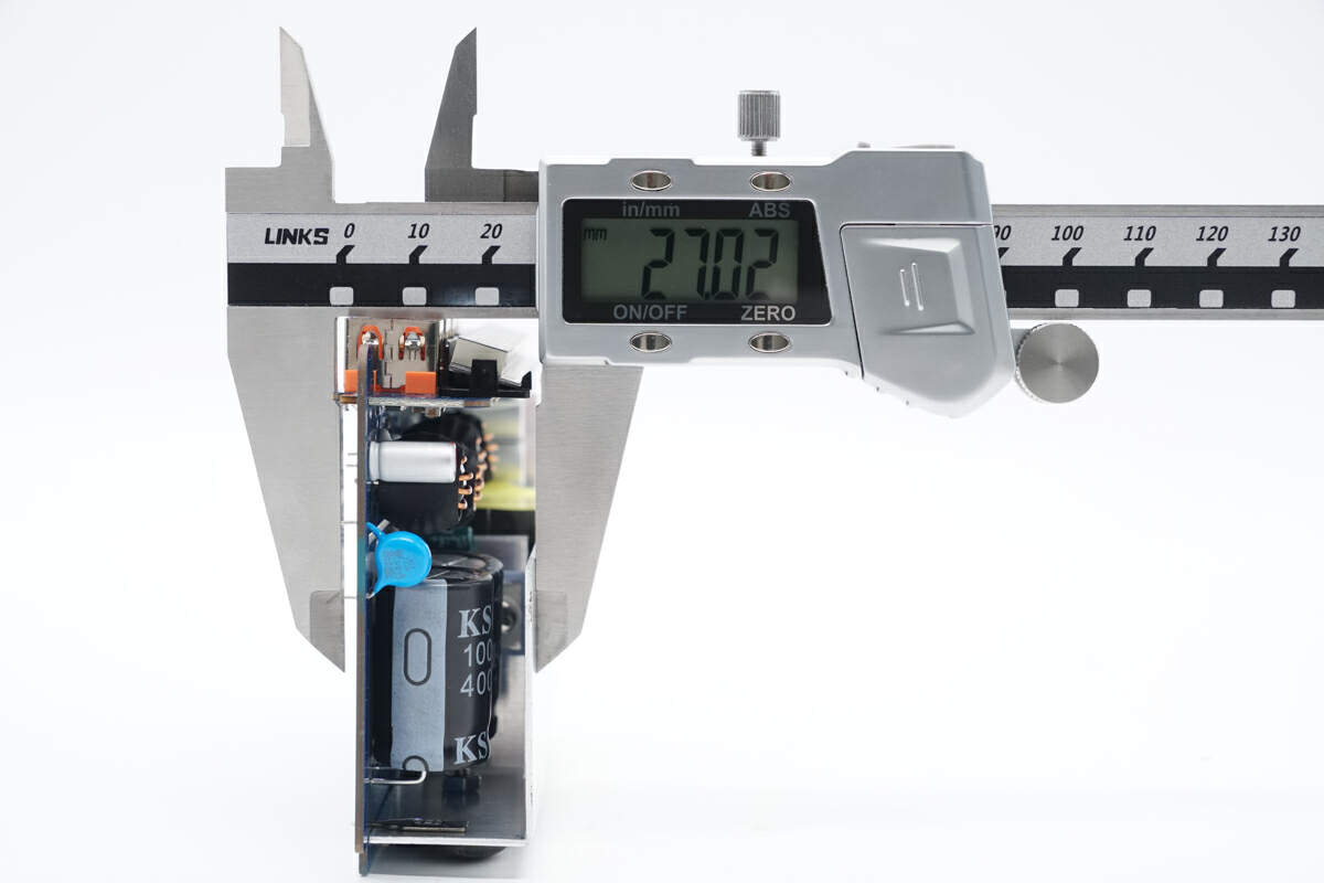
The thickness is about 27 mm (1.06 inches).
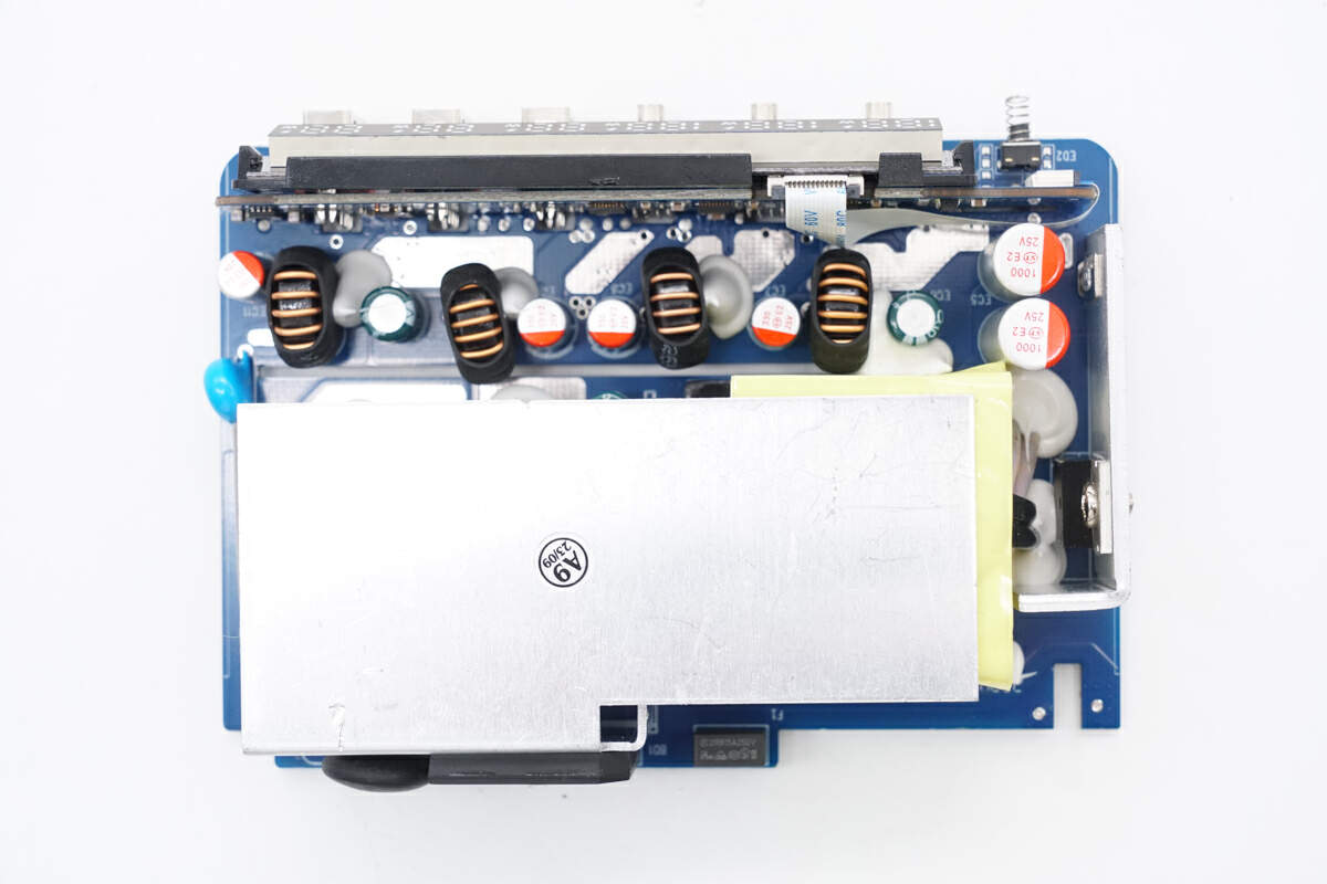
There are fuse, bridge rectifier, NTC thermistor, synchronous rectifier, capacitor, and inductor on the front.
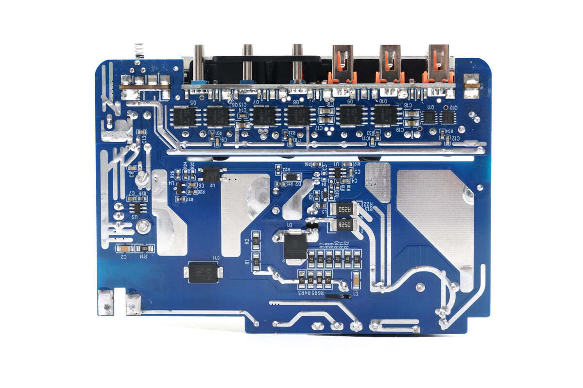
The master control chip, synchronous rectifier controller, SMD Y capacitor, feedback optocoupler, and synchronous buck MOSFET are on the back.
ChargerLAB found it adopts a QR flyback topology, with synchronous rectification and fixed voltage output. And it has four buck circuits.
Next, take a look at each component, starting from the input end.
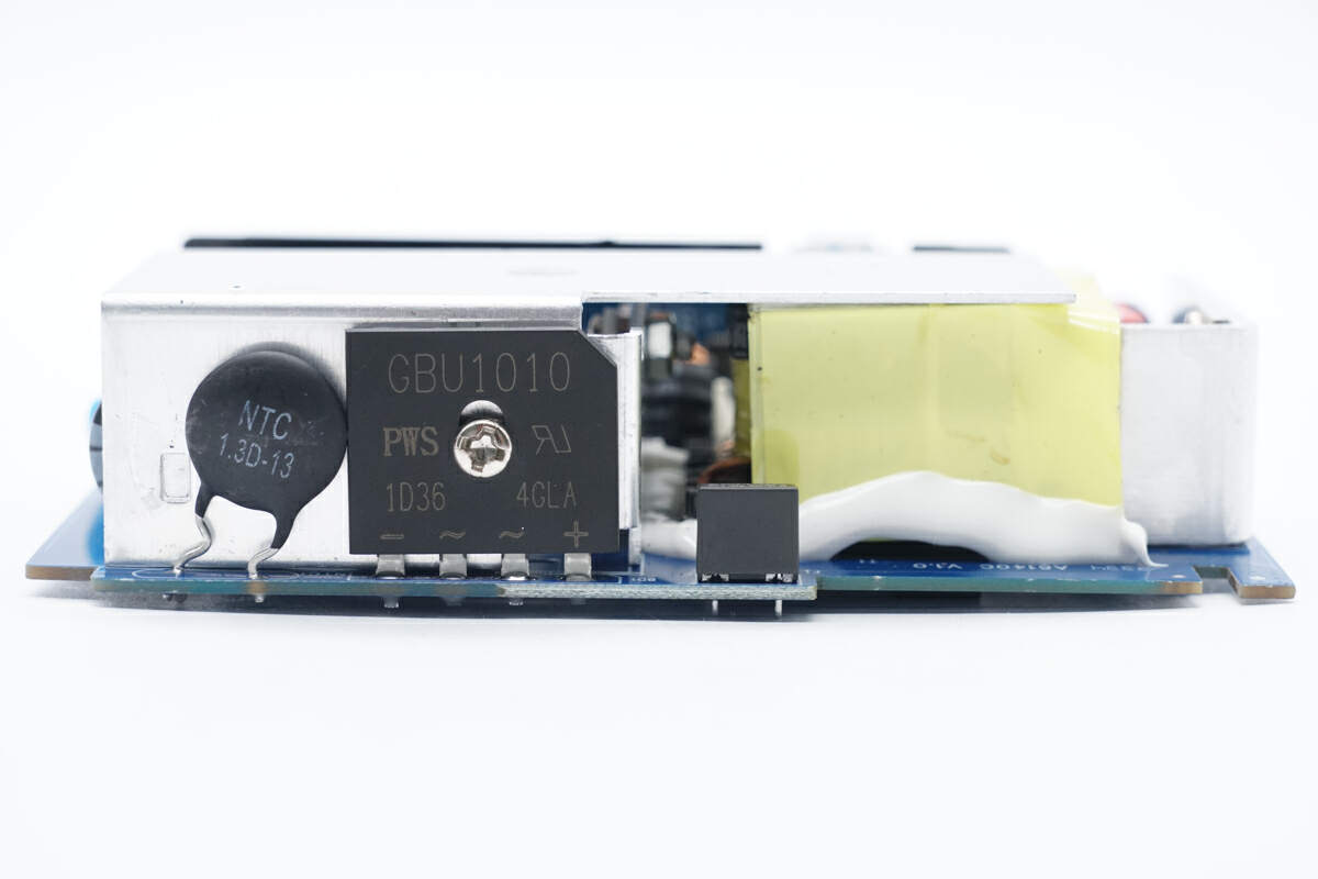
There are fuse, bridge rectifier, and NTC thermistor on the side of the PCBA.
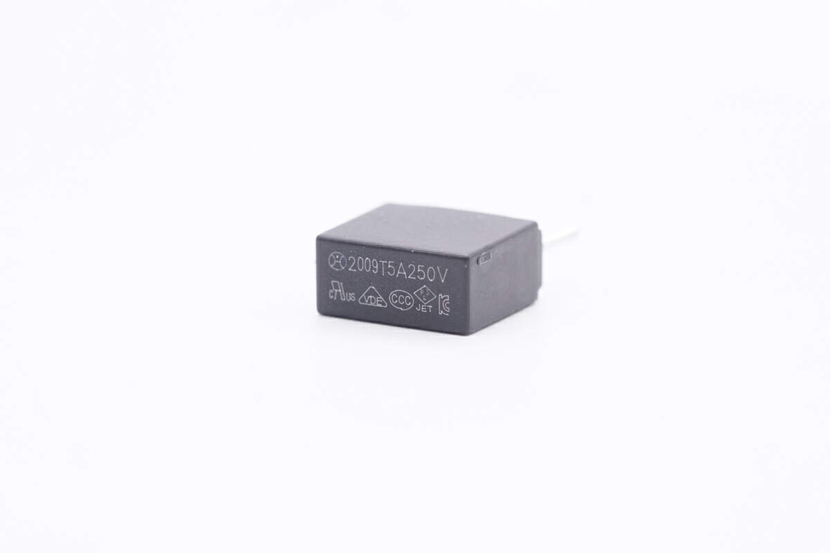
The specification of the input fuse is 5A 250V.
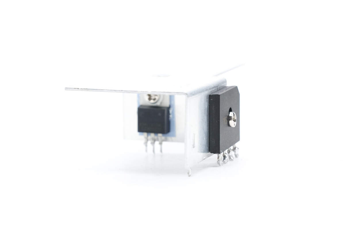
The primary MOSFET and bridge rectifier are on this heat sink.
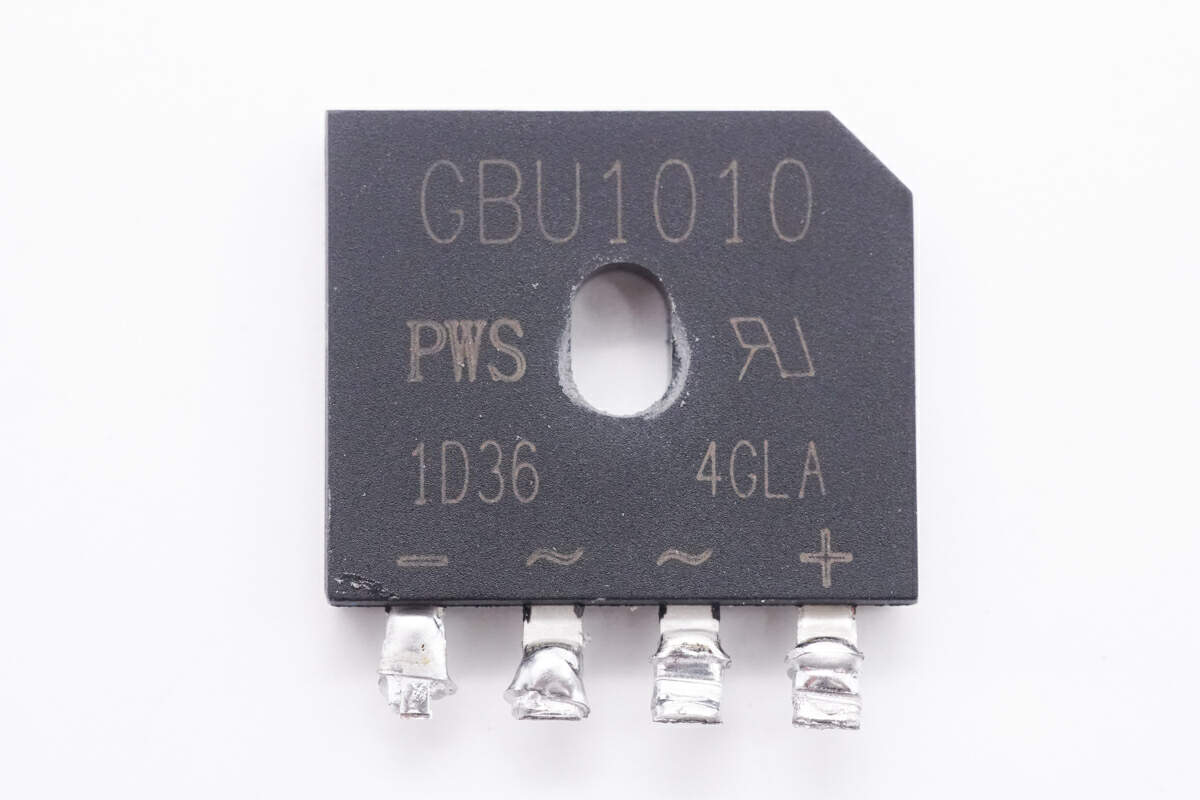
The model of the rectifier bridge is GBU1010. 1000V 10A.
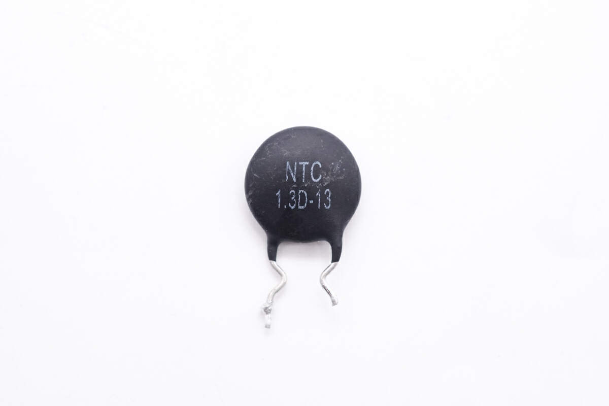
The NTC thermistor is used to suppress the surge current when powering on.
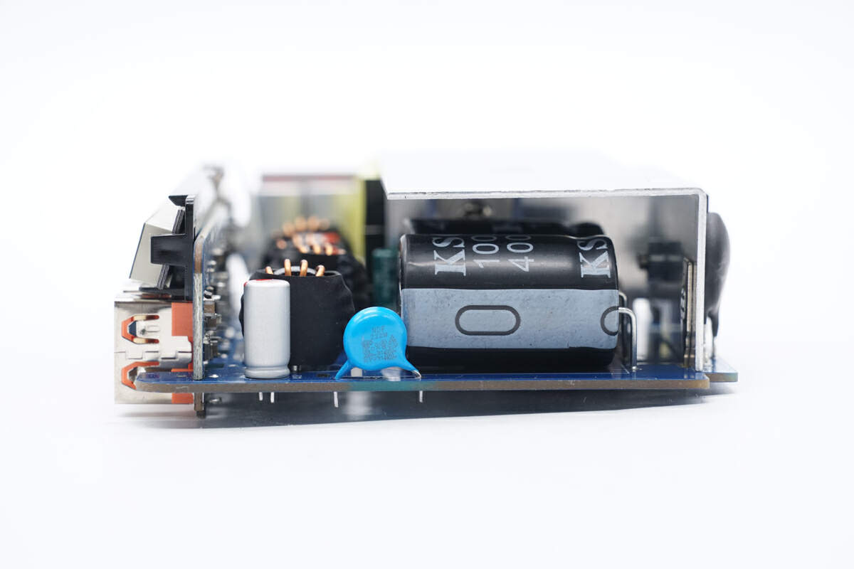
Two electrolytic capacitors for input filtering are under this heat sink.
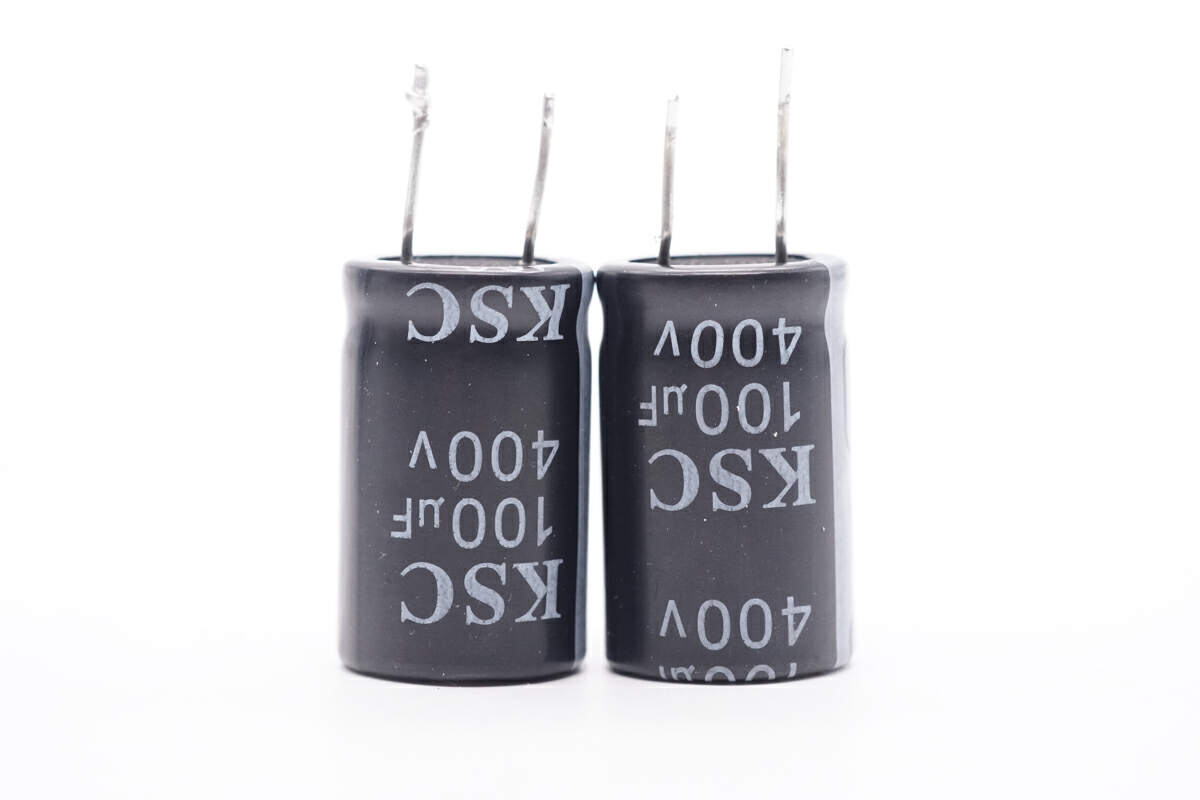
They are from KSC. 400V 100μF.
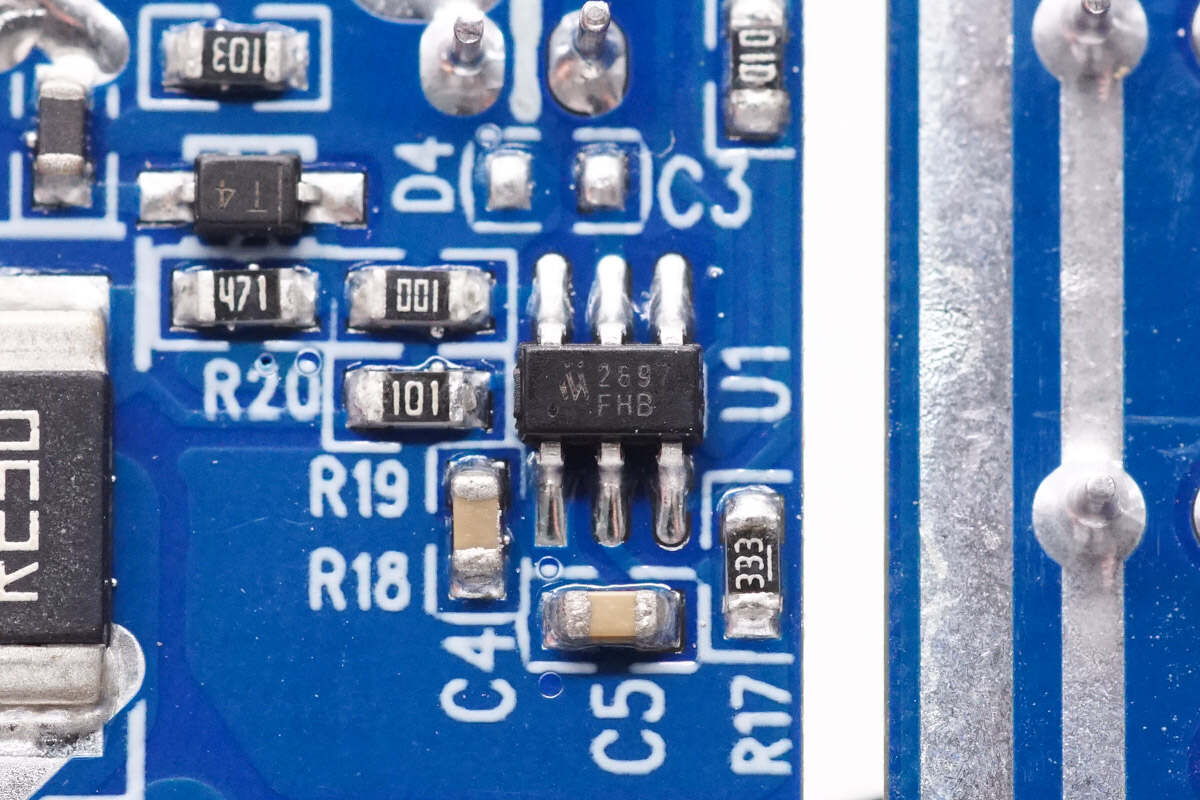
The master control chip is from Meraki and is a QR PWM controller optimized for PD fast charging. It supports a wide VCC voltage range of 9V to 90V. It can cover the output range of PD/PPS from 3.3V to 23V and there is no external voltage buck circuit required. Model is MK2697.
It adopts Meraki's own drive technology. It can also support up to 200kHz.
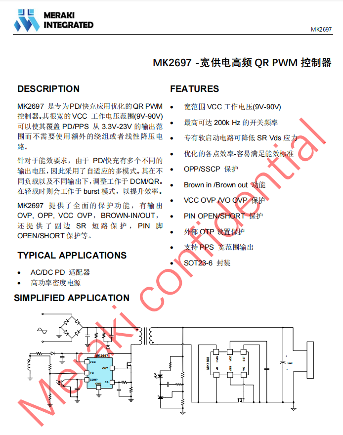
It has adaptive multi-mode to cope with different output voltages. It can adjust the QR mode under different loads and different outputs. It will adjust to burst mode under light load to improve efficiency.
It provides OVP, OPP, VCC, OVP, BROWN-IN/OUT, SR short circuit protection, and OPEN/SHORT protection of pin.

The filter capacitor that powers the master control chip is from Guike. 50V 10μF.
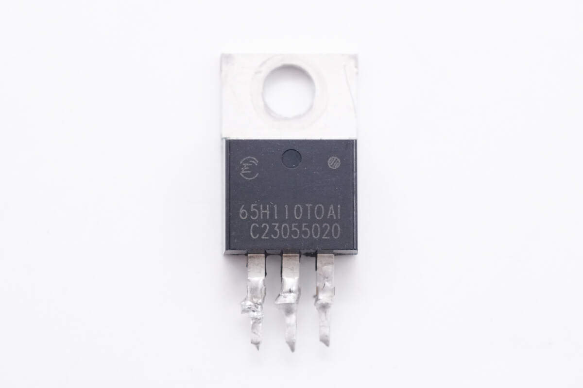
The GaN FET is from CorEnergy and adopts TO220 package. Model is CE65H110TOAI. 650V 110mΩ.
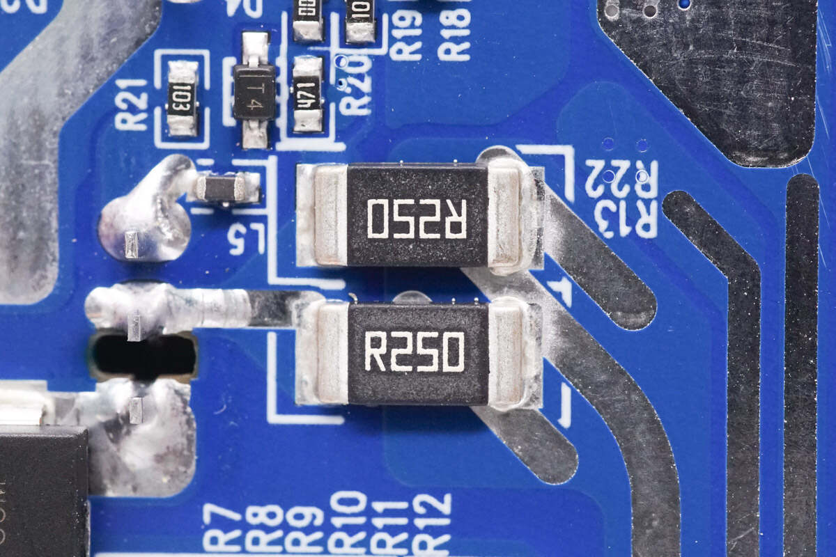
These two sampling resistors are used to detect the current of primary side. 250mΩ.
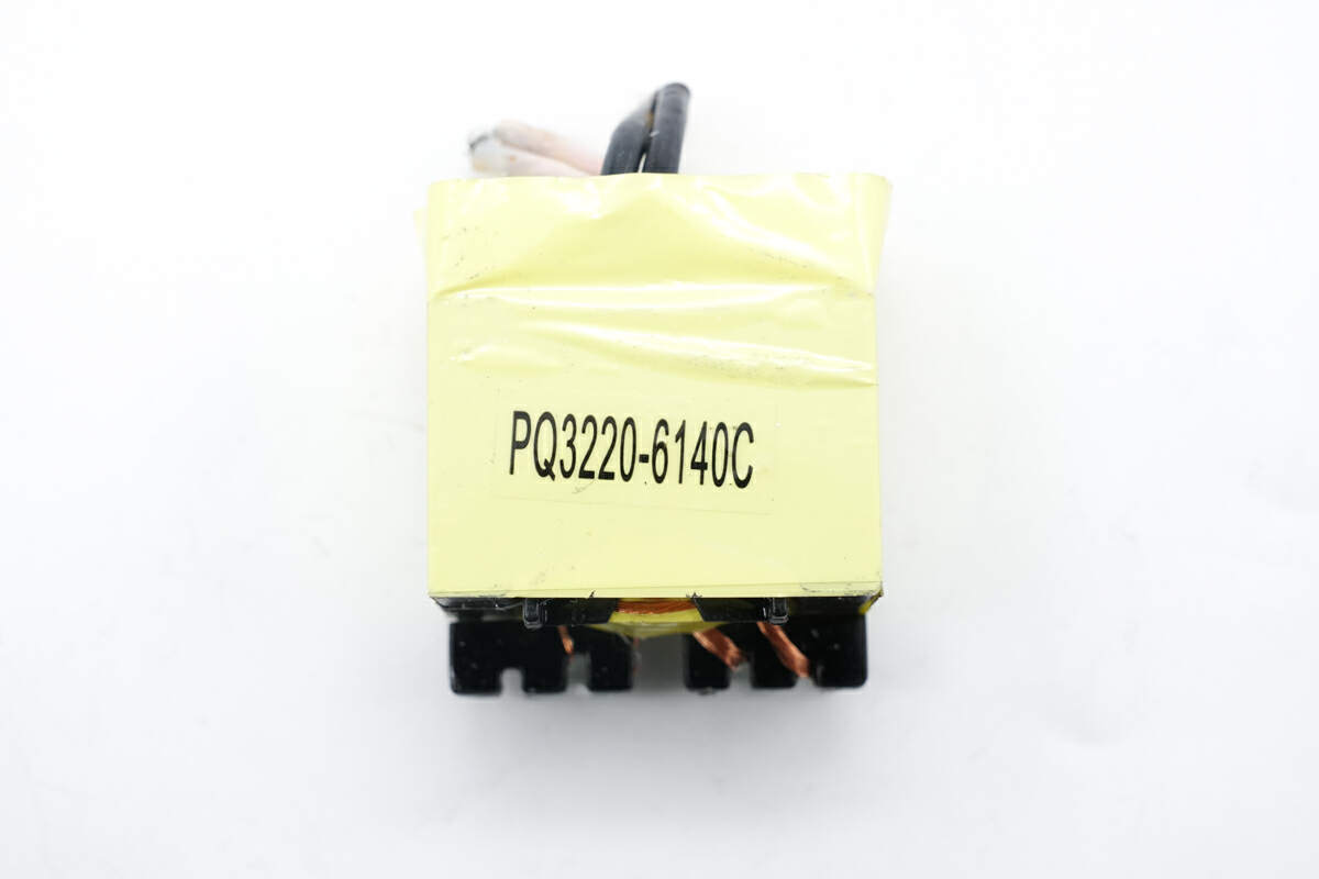
The transformer adopts PQ3220 magnetic core and insulation by tape.
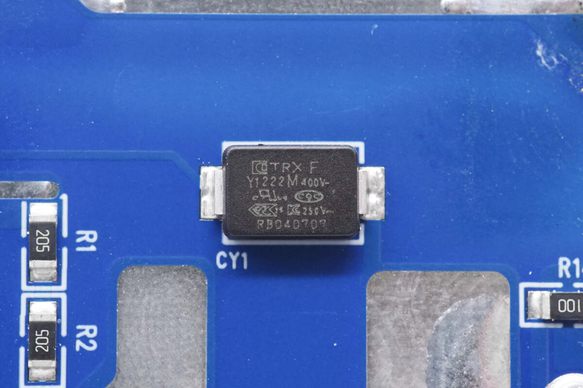
The SMD Y capacitor is from TRX. Its small size and light weight are suitable for high-density power products such as GaN fast chargers. Model is TMY1222M.
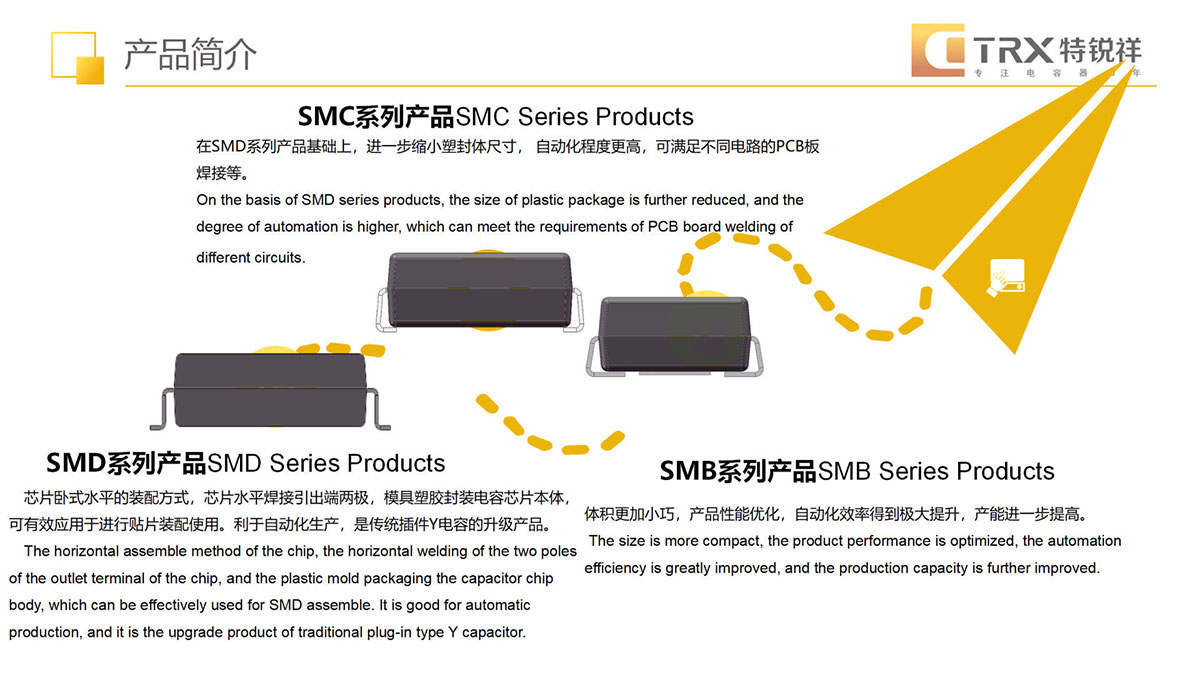
Here are some information about TRX products.
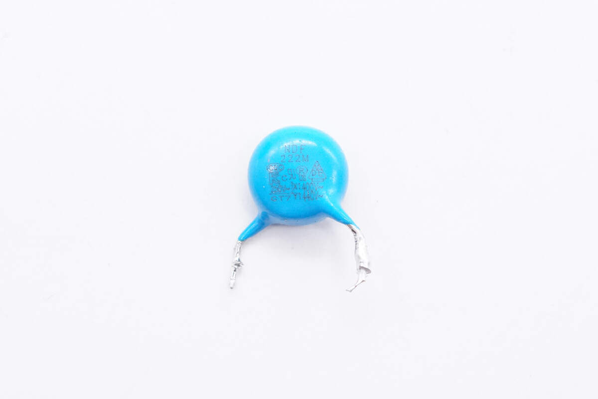
The blue Y capacitor is from NDF.
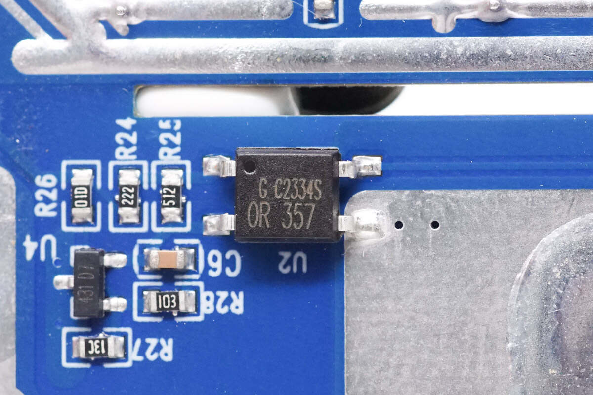
The optocoupler marked with 357 is from OR and is used for output voltage feedback.
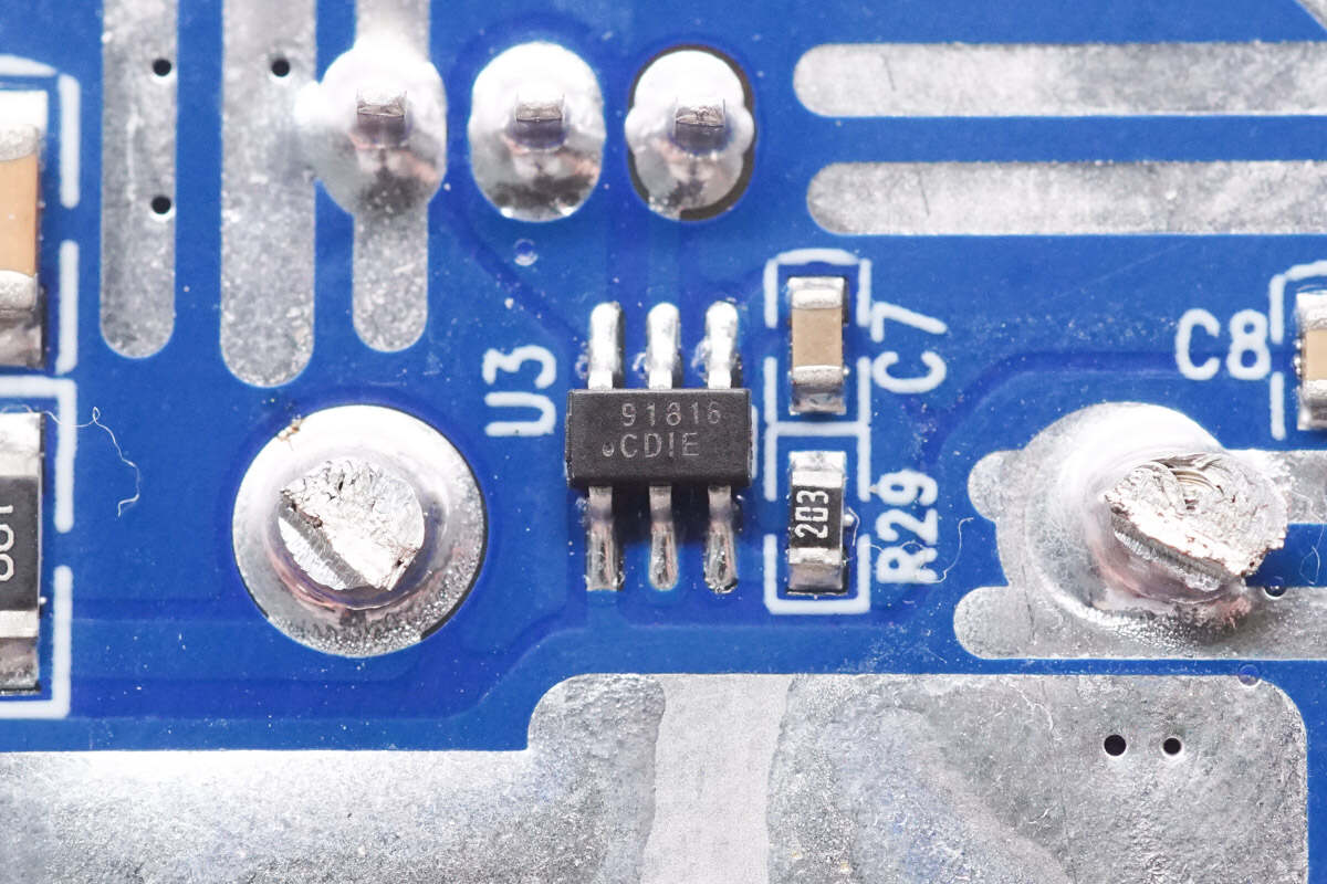
The synchronous rectifier controller is from Meraki. It adopts flyback topology and is compatible with CCM, DCM, and QR modes. It adopts Meraki's own self-powering technology to power VCC and there is no external auxiliary winding required. Model is MK91816.
It has 10nS turn-off delay and 4A high sink current. It can maximize the on-time of the external MOSFET to improve high efficiency. And it can independently detect current ringing in DCM to prevent accidental activation.
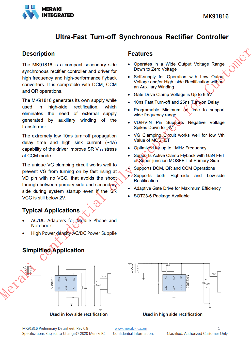
Here is the information about Meraki MK91816.
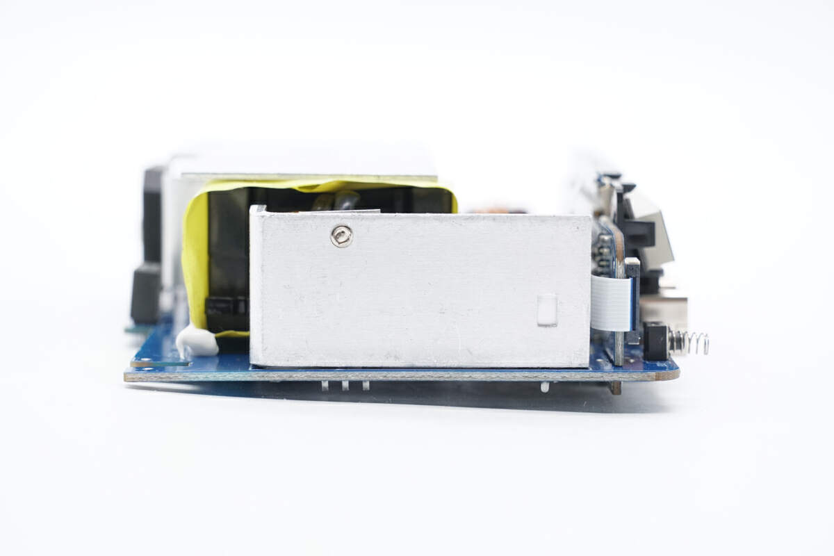
There is another heat sink on the side of the PCBA module.
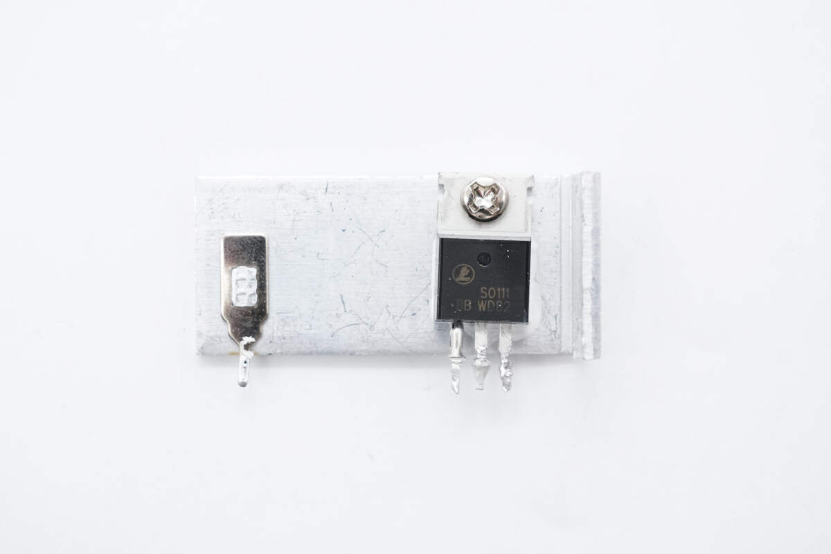
The synchronous rectifier is screwed on the heat sink.
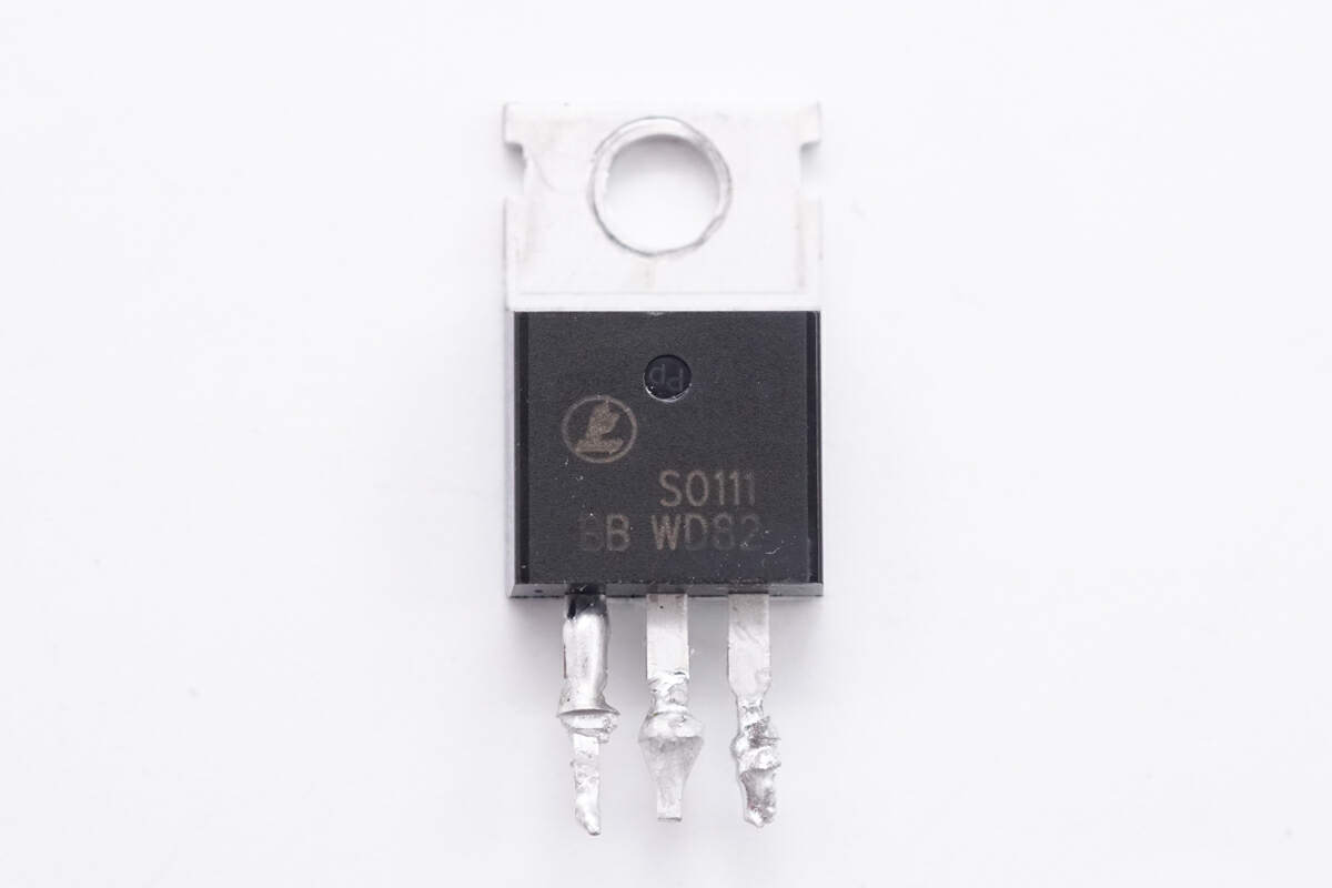
It is from Leadteck and marked with S0111. It adopts TO220 package.
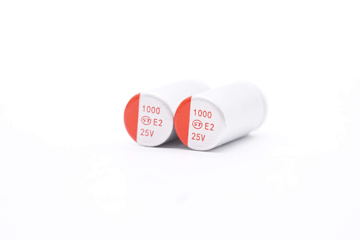
These two solid capacitors for output filtering are from ST E2 series. 1000μF 25V.
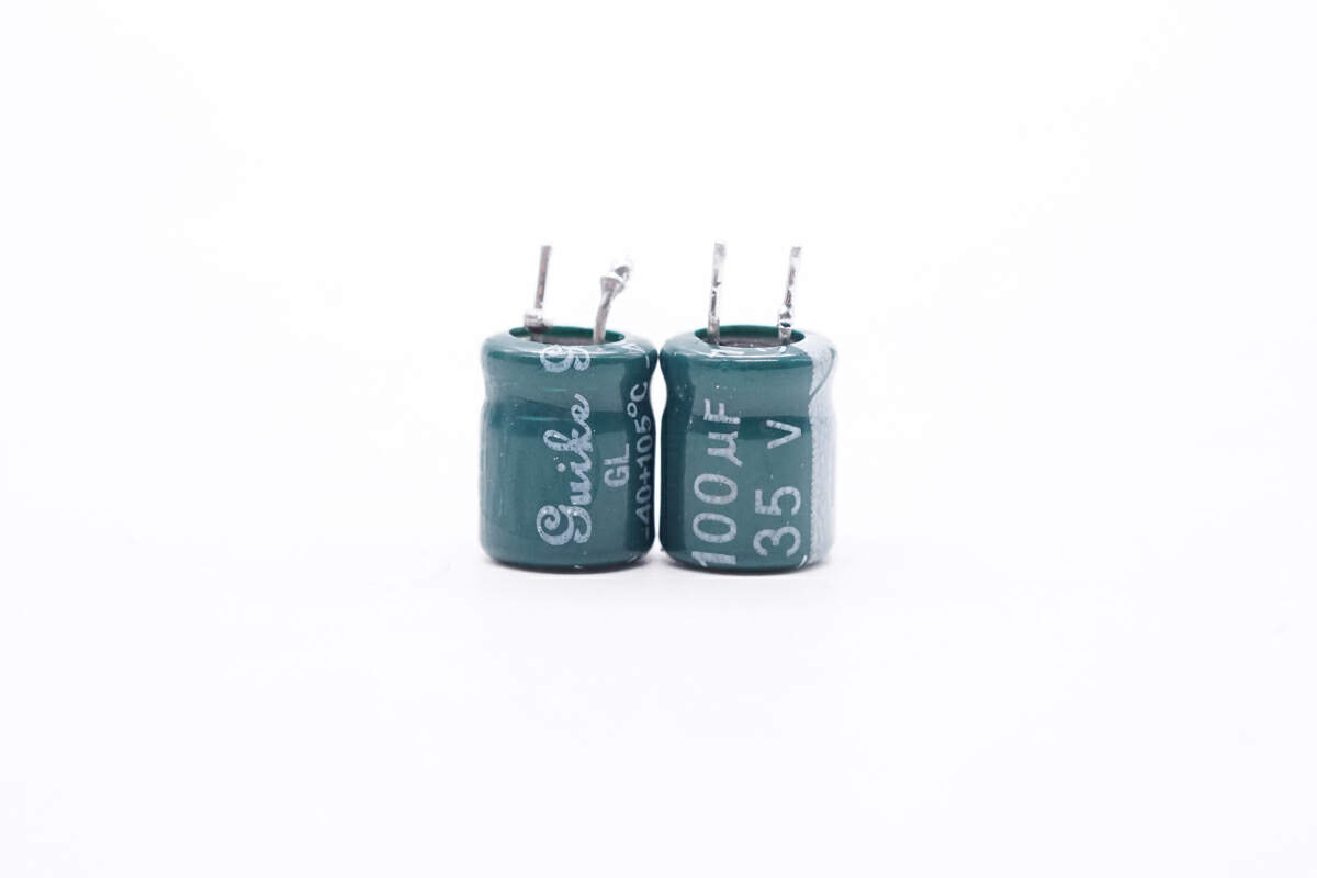
These two electrolytic capacitors for input filtering are from Guike. 100μF 35V.
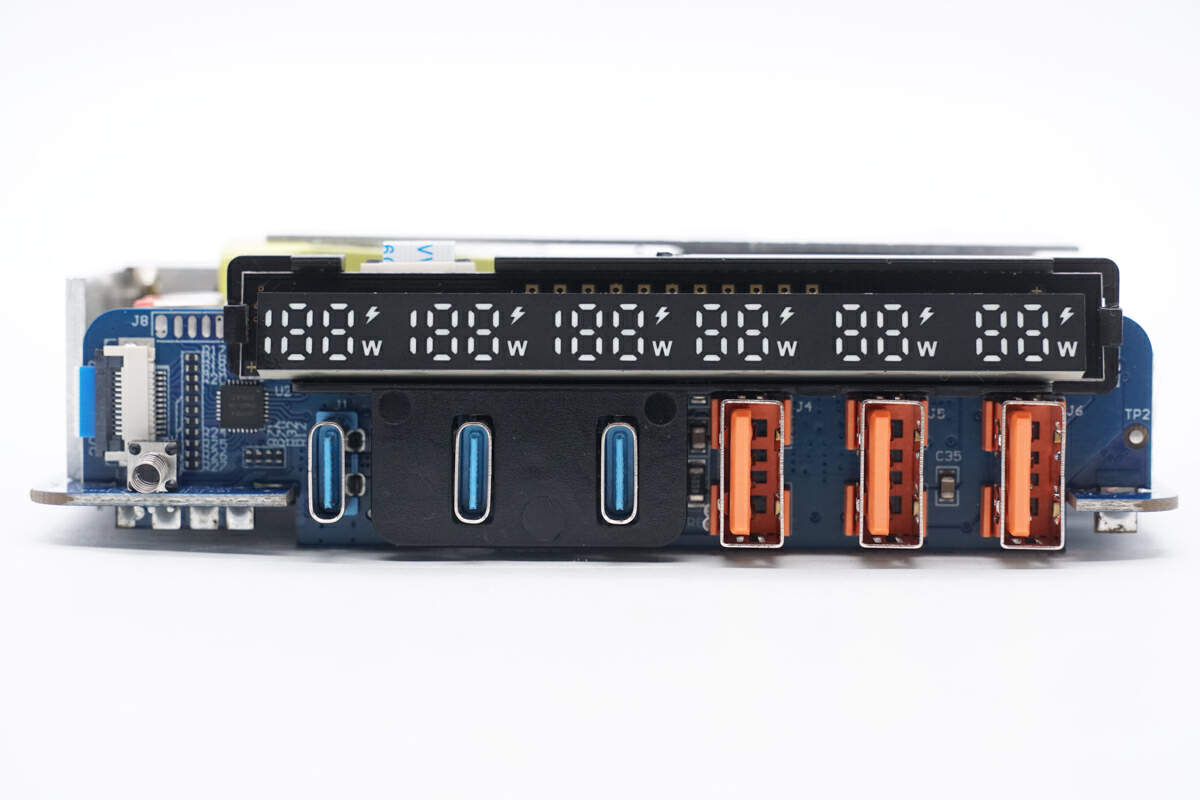
There is the small PCB of the display and sockets at the output end.
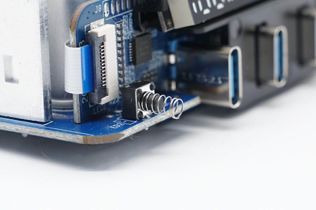
The power button is soldered on the small PCB.
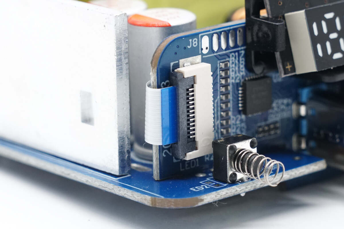
The flat cable is used to connect the display.
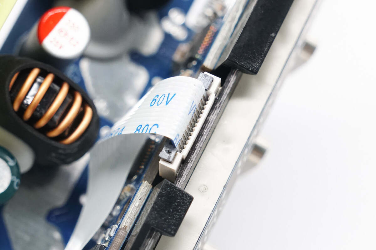
This is the other side of the flat cable.
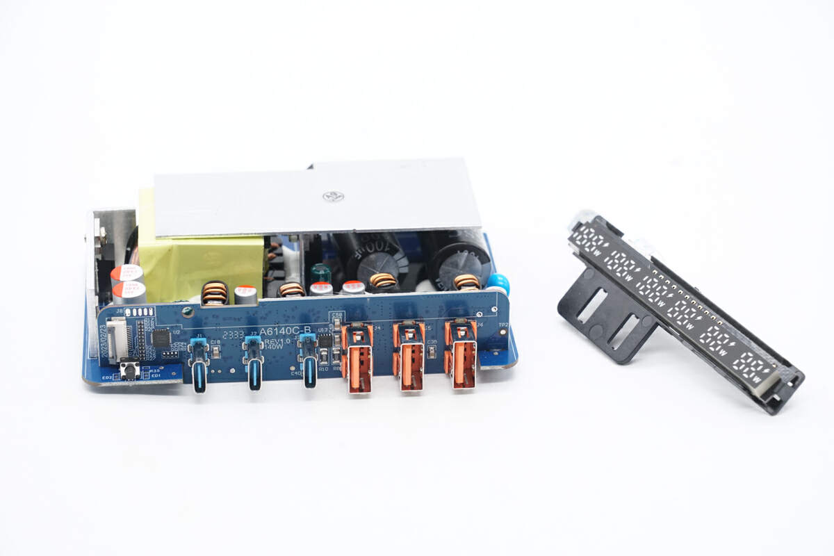
Remove the display.
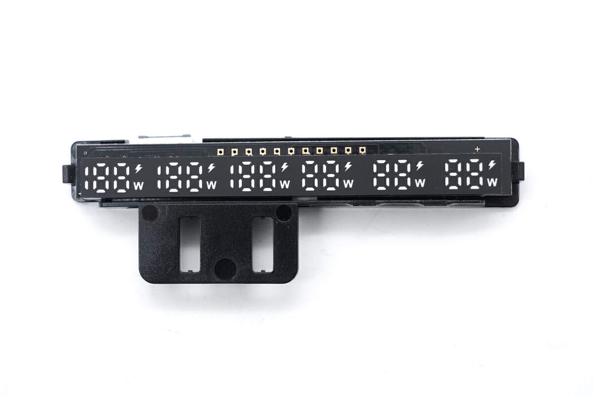
It is fixed on a plastic frame.
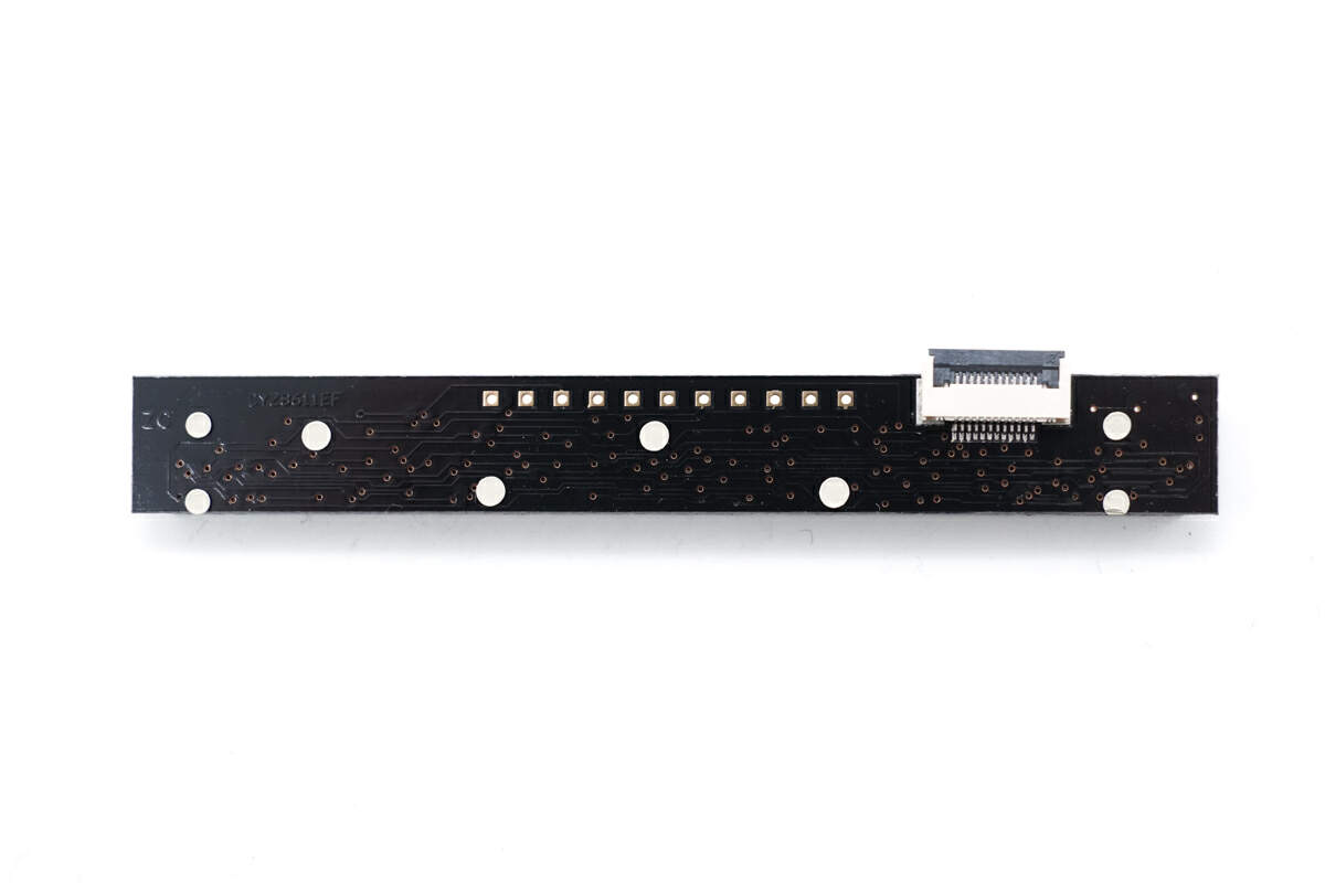
Take out the PCB of the display, the display grille is fixed by hot melt.
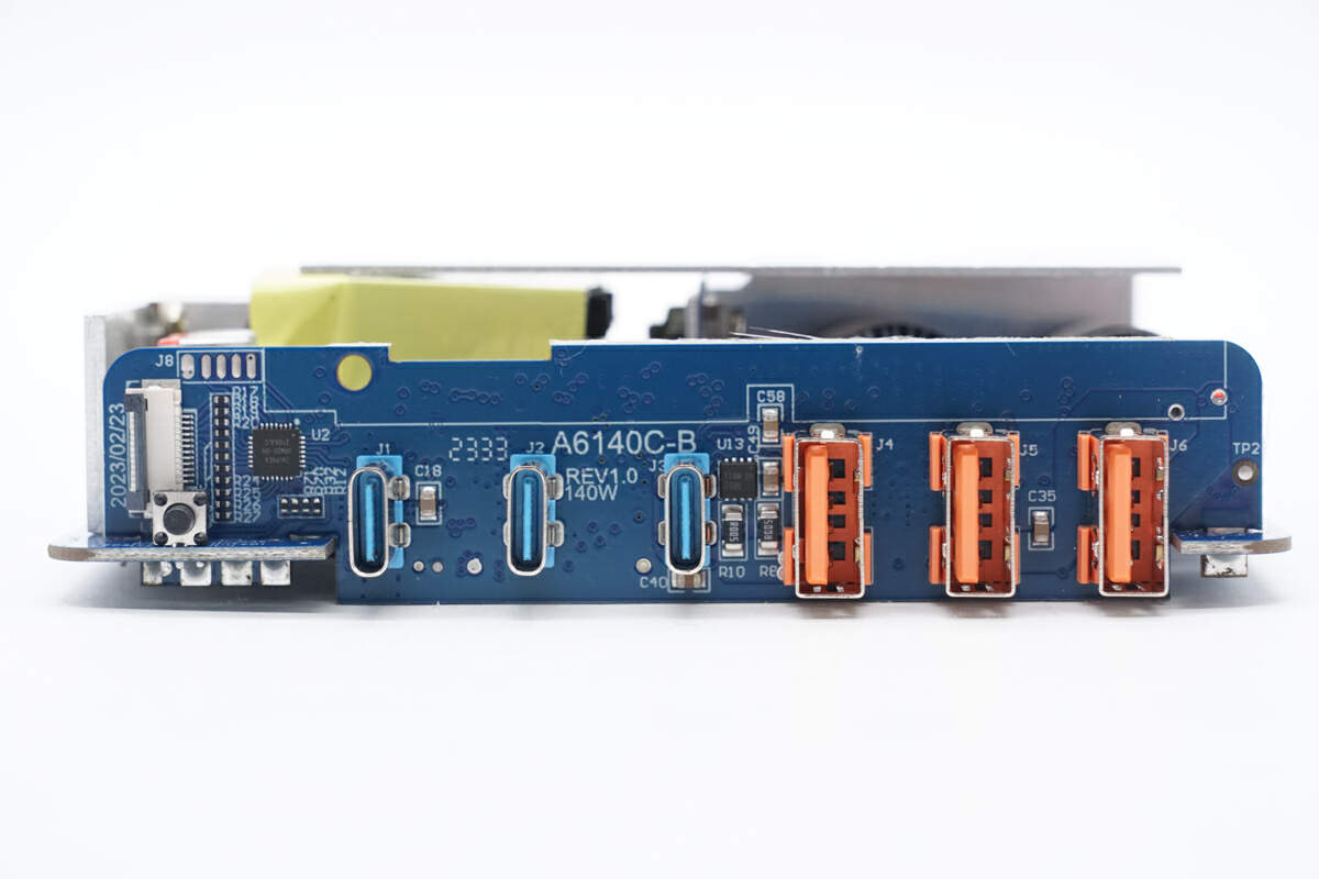
The small PCB of ports is vertically soldered on the PCBA module.
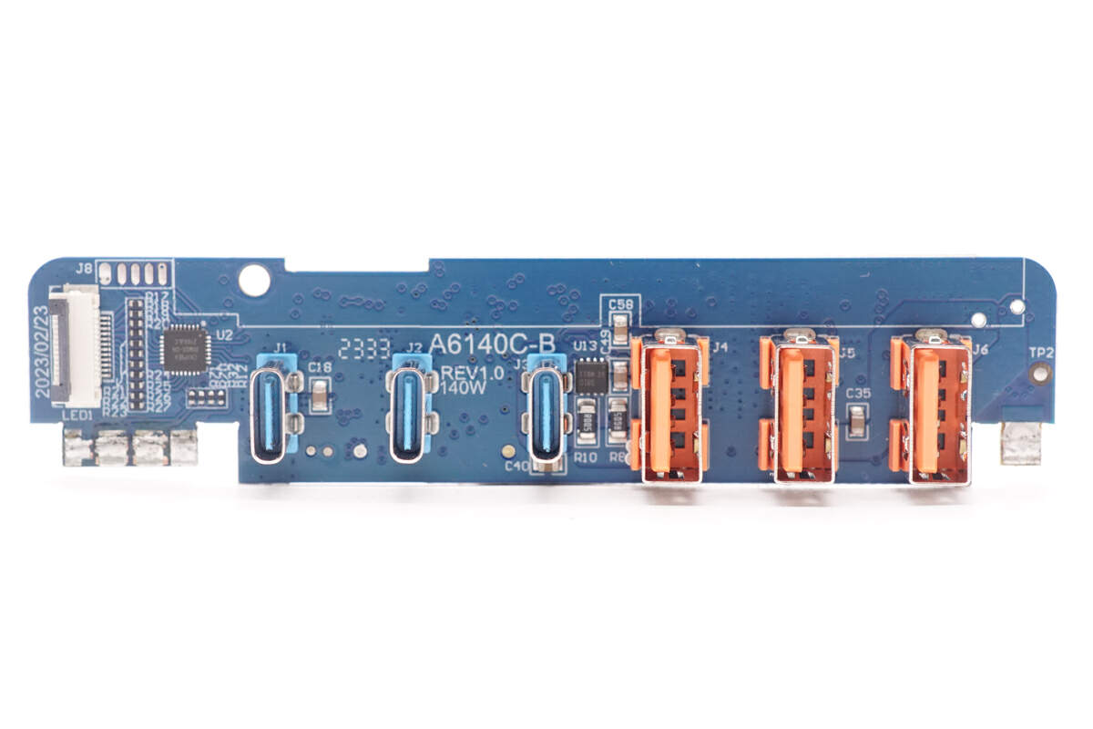
Remove this small PCB, there are MCU, sockets, and VBUS MOSFET.
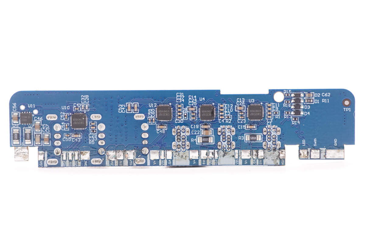
The buck protocol chips and VBUS MOSFET are on the back of the small PCB.
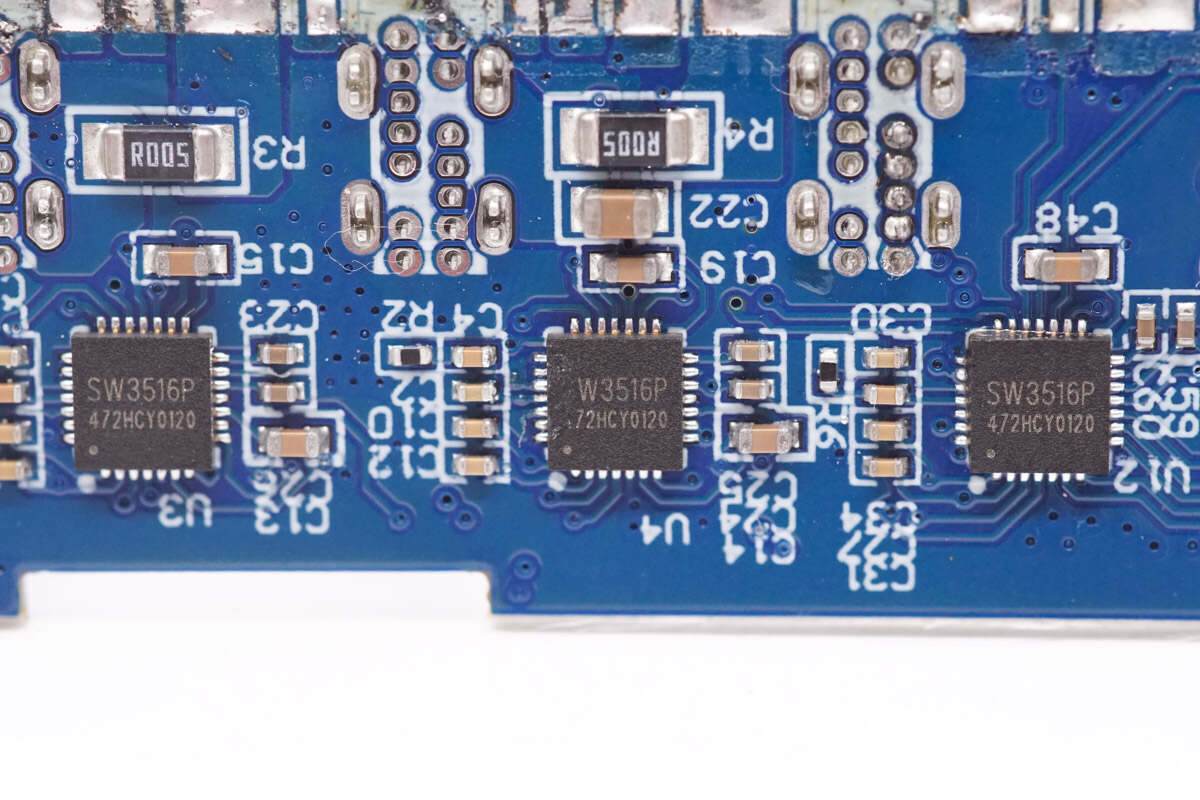
Three buck protocol chips for three USB-C ports are from iSmartWare. They are highly integrated multi-protocol dual-port charging chips that support fast charging of any USB-C and USB-A ports. They also support dual-port independent current limiting. Model is SW3516P.
It integrates 5A high-efficiency synchronous buck converter. It supports output of PD 100W and CC/CV modes. It supports PPS, PD, QC, AFC, FCP, SCP, PE, SFCP, and other fast-charging protocols.
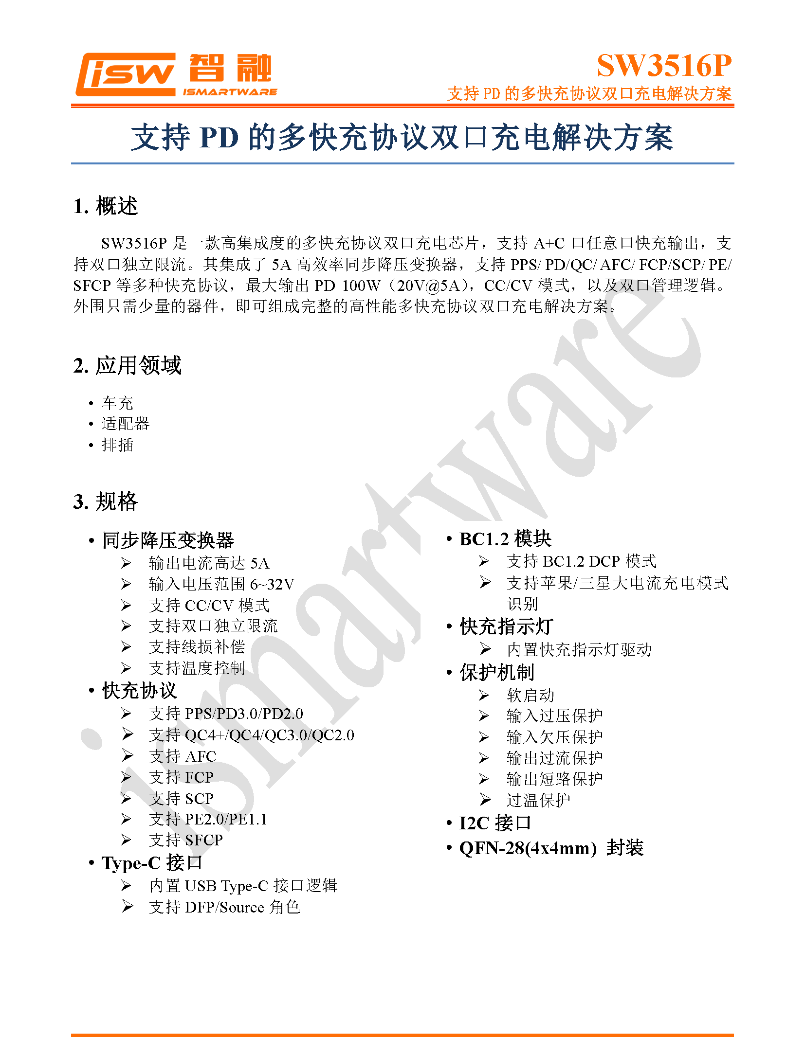
Here is all the information about the iSmartWare SW3516P.
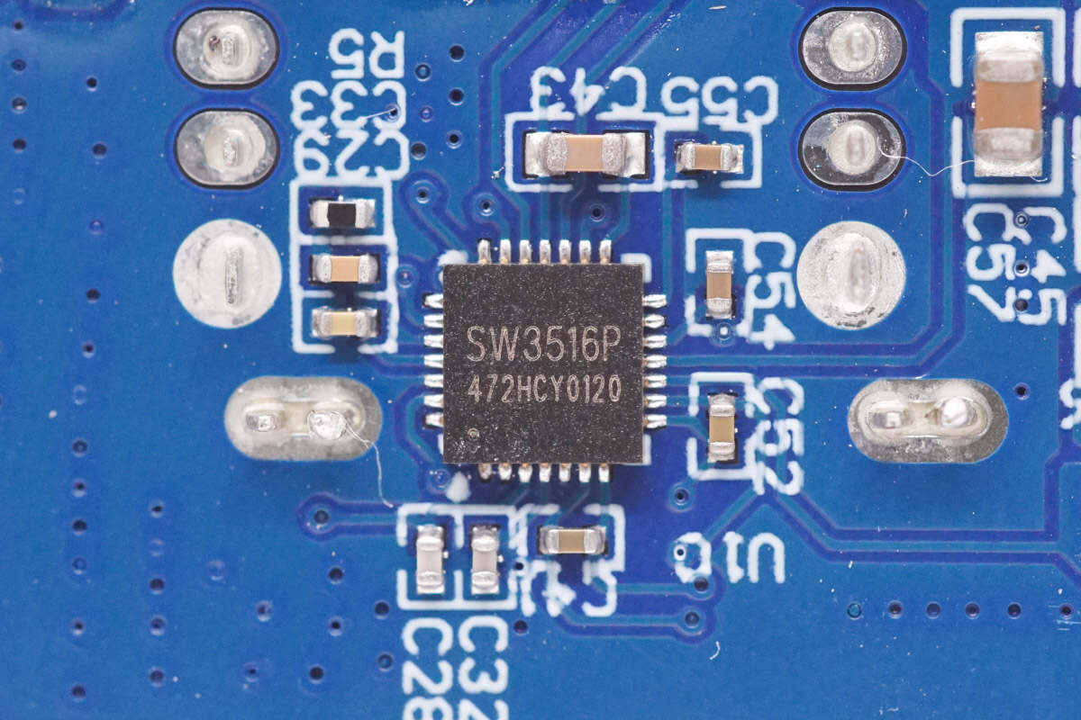
The buck protocol chip of the USB-A port is the same as that of the USB-C ports.
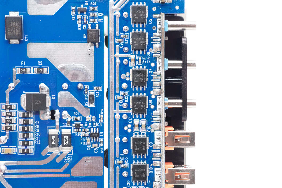
There are six synchronous buck MOSFETs for three USB-C ports.
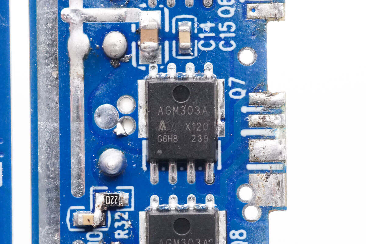
The synchronous buck MOSFET is from AGM-Semi and adopts DFN5 x 6 package. 30V 2.7mΩ. Model is AGM303A.
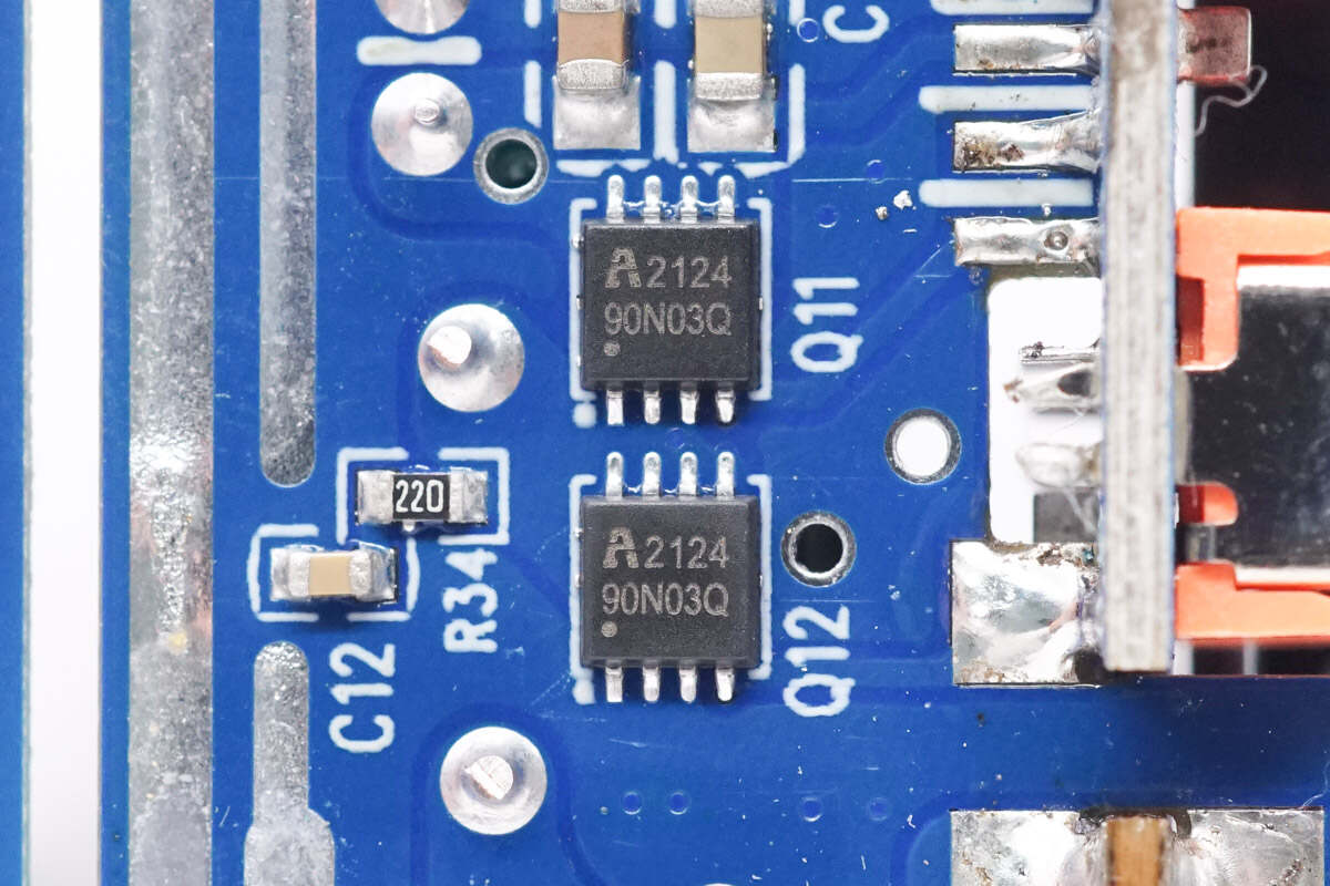
The synchronous buck MOSFETs for USB-A are from All Power and adopt PPAK3 x 3 package. 30V 4.2mΩ. Model is AP90N03Q.
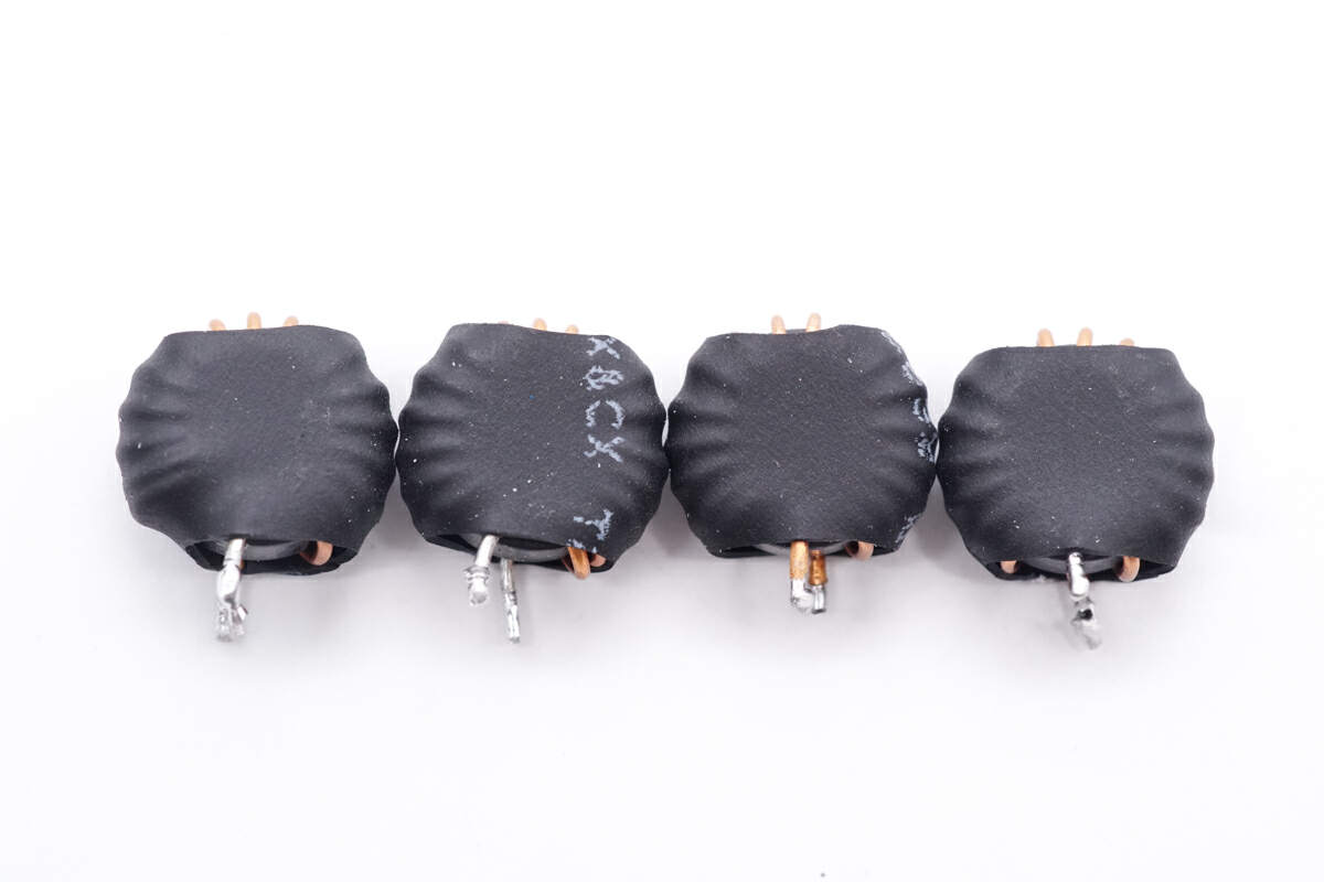
These four buck inductors correspond to four buck circuits respectively.

These four solid capacitors for output filtering are from ST E2 series. They correspond to four outputs. 330μF 25V.
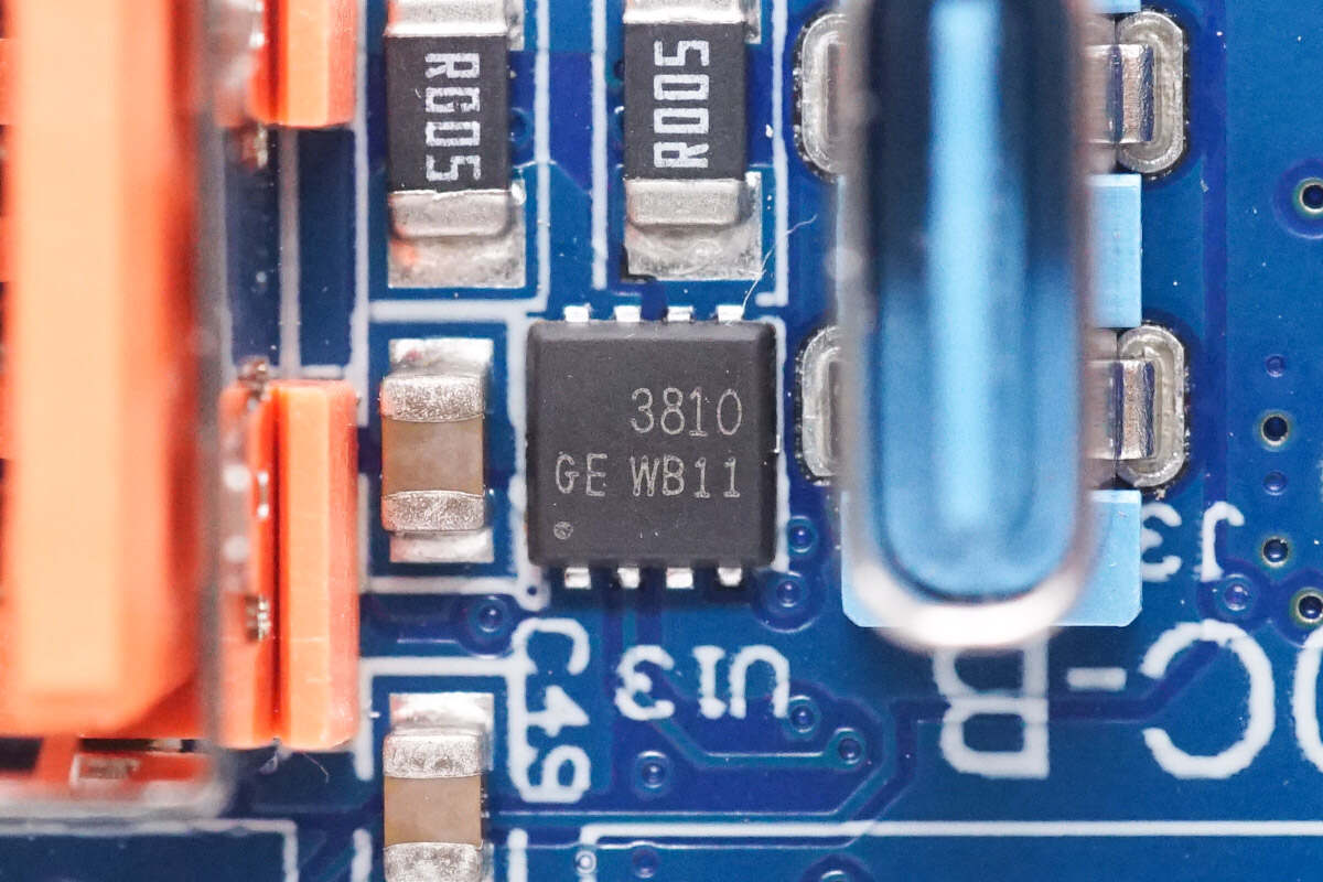
The VBUS MOSFET is a dual MOSFET and is marked with 3810.
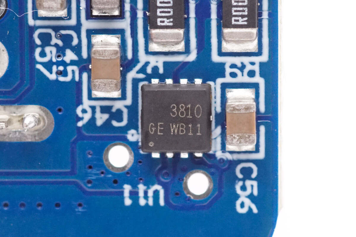
The other VBUS MOSFET has the same model.
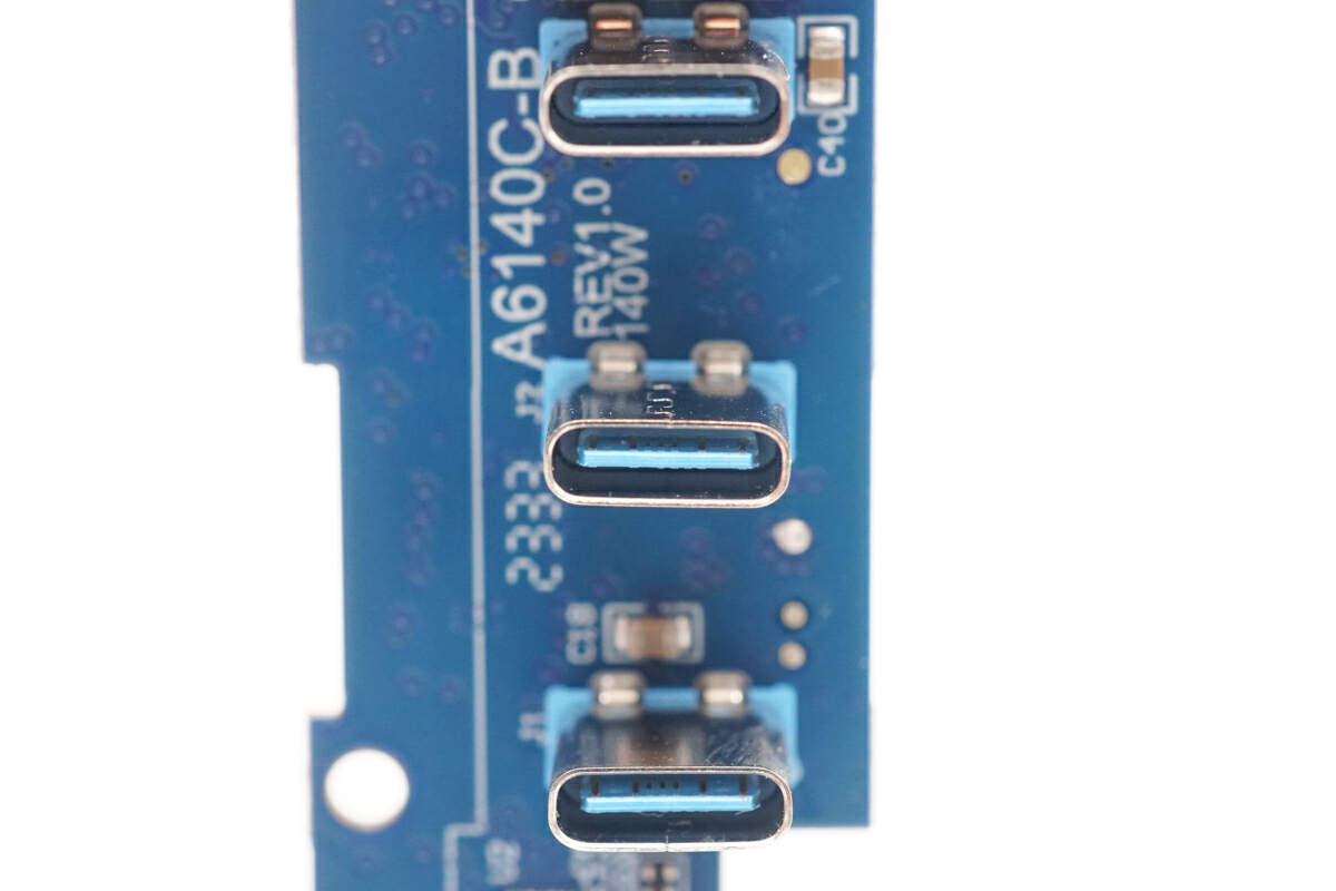
The plastic sheets of USB-C sockets are blue.
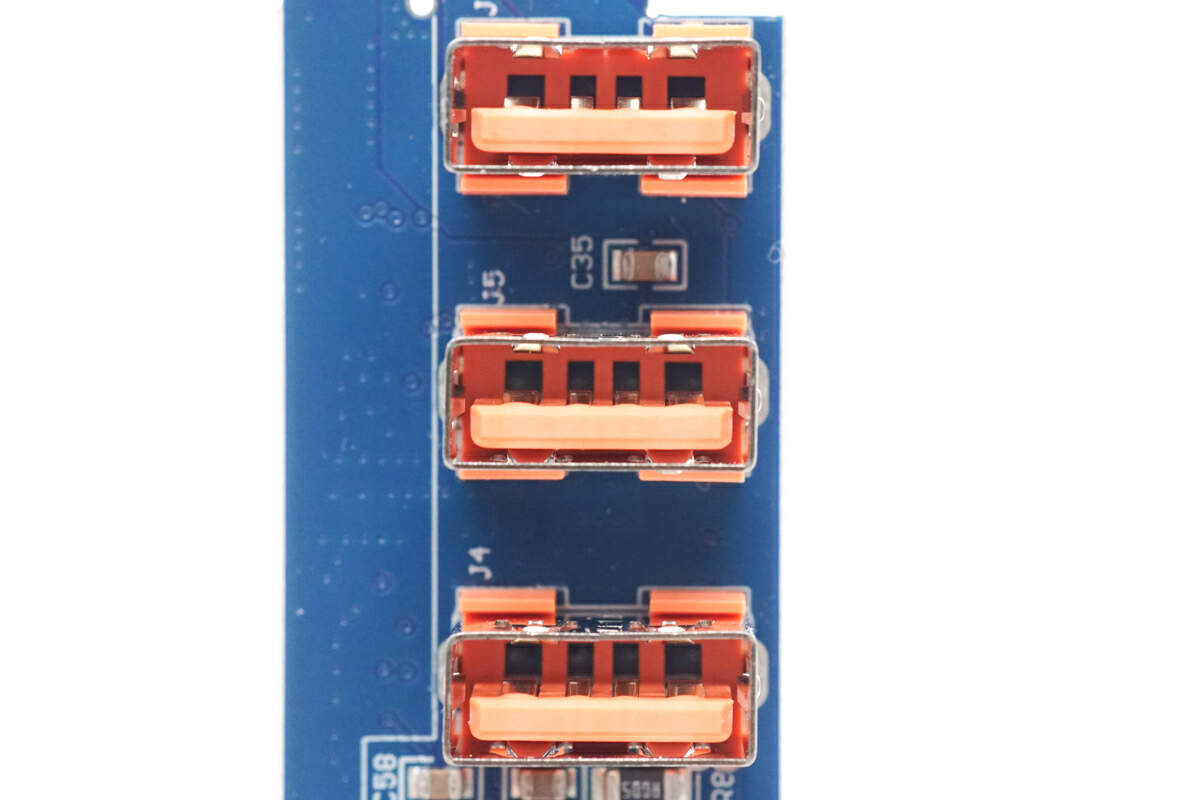
The USB-A sockets are orange and they have widened pins.
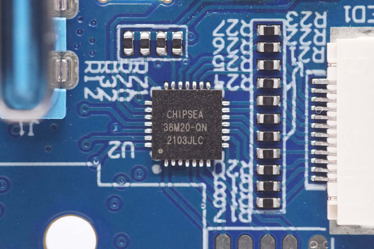
The 8-bit MCU used for display and auto power control is from Chipsea. It integrates 12-bit ADC, 8K×16-bit MTP, 1K bytes SRAM, and 256 bytes E2PROM. Model is CSU38M20.
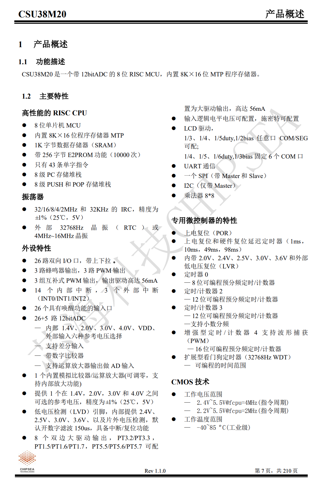
Here is all the information about the Chipsea CSU38M20.
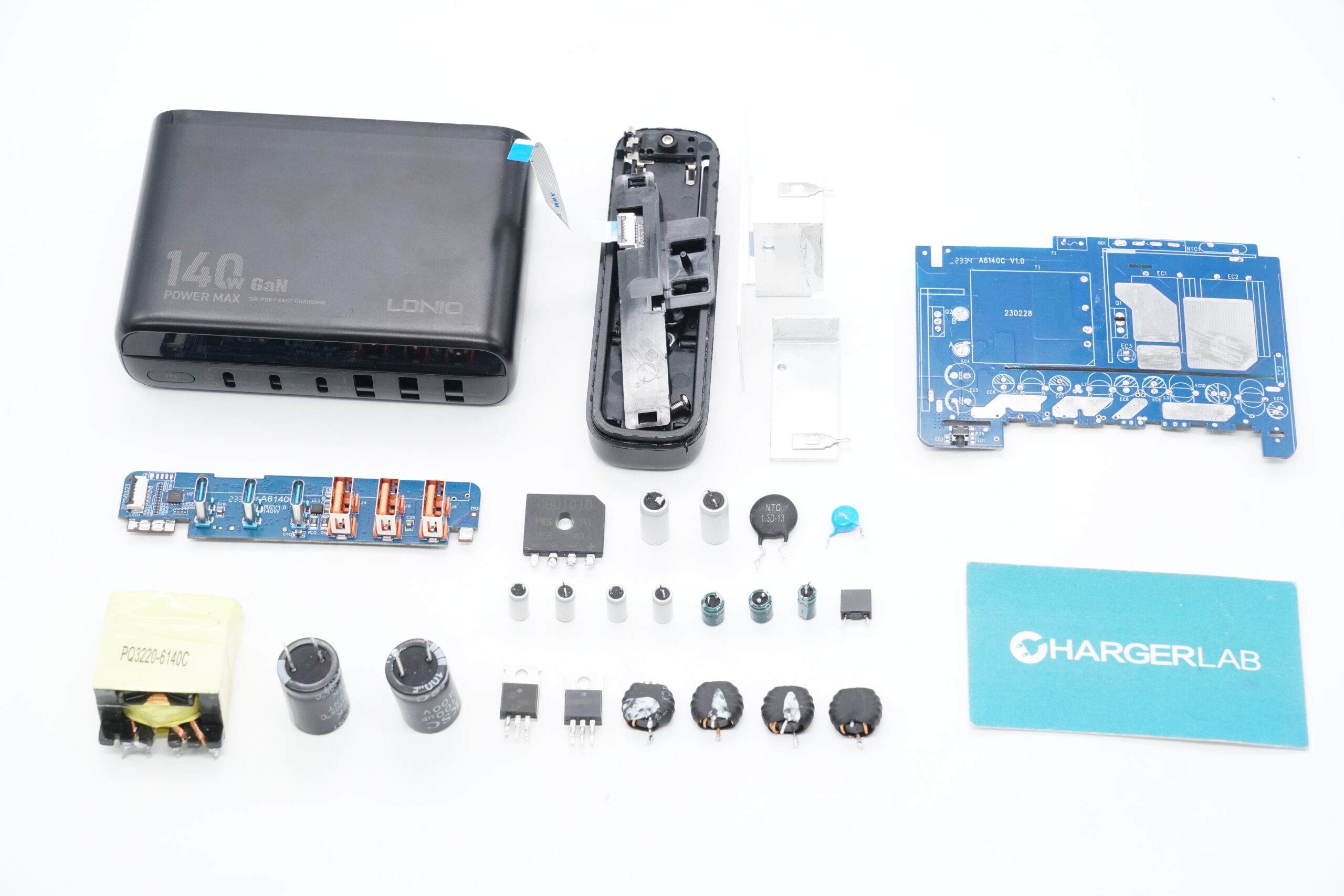
Well, those are all components of this charger.
Summary of ChargerLAB
This charger is equipped with a power cord and replaceable plugs. You can use it on the desktop or carry it out. The replaceable plugs can help you travel to different counties and regions. It also has a display for you to check the real-time charging power of each port.
The charger adopts QR flyback topology. It has four independent buck circuits to achieve six-port fast charging output and automatic power distribution. There are two heat sinks inside the charger for heat dissipation. If you have a lot of devices that need to be charged at the same time, it's a smart choice.
Related Articles:
1. Teardown of DELL 165W PD3.1 GaN Power Adapter (LA165PM210)
2. Teardown of Anker 150W GaNPrime 747 Charger (A2340)
3. Teardown of AOHi 65W Ultra-thin GaN Charger (AOC-C013)

