Recently, ChargerLAB has got hands on the AC adapter with built-in battery, which applies GaN technology from L Lab Corporation.
This product has packed together a 60W AC charger and a 10000mAh battery pack.
It has dual USB-C output ports. Either of the USB-C ports could achieve max output at respective mode (charger mode or power bank mode). It's very convenient for daily use.
At AC charger mode, either of the USB-C ports is capable of outputting 60W power, which in other words, it could power most of the laptops.
While at power bank mode, you would have the choice of either powering your laptop at 40W through a single USB-C port, or two iPhone 12 at 20W through each of the USB-C ports.
One of the awesome features of the product, in terms of futuristic technology, is the use of innovative technology – DC Bypass Topology. The DC bypass topology, compared to conventional type, it could achieve DC to DC parallel powering through independent reference source without the need of any ICs. In overall, the system efficiency, with the DC bypass topology, has increased by 3-4%, which is remarkable in AC adapters.
Let's do the teardown on the product to see how the design looks.
- Overview of the product

The enclosure of the product is polycarbonate (PC) material. There is a grey plastic panel with matte finishing at the output ports for cosmetic purpose. With properly rounded edges and corners, grip and touch are friendly for users.

At the center of the product is the capacity LED indicators, with product name and touch sensor instruction at the bottom. By touching the sensor area, the blue capacity indicator will light up.

On the bottom side of the enclosure, marks the rating.
Model: PST-60C2PB
AC Input: 100-240V~50/60HZ
USB-C Input: 5/9/12V 18W Max
Battery charging spec: 8.4V2A Max
At AC adapter mode:
USB-C1/C2 Output: 5V3A、9V3A、12V3A、15V3A、20V3A Max
Total output: 60W Max
At Powerbank mode:
USB-C1/C2 Single port only output: 5V3A、9V3A、12V3A、15V2.67A、20V2A Max
USB-C1/C2 output):5V3A、9V2.22A、12V1.67A
Total output: 40W Max
Battery capacity: 9600mAh
The product has been certified for CE, FCC, ETL, ROHS, and DOE VI.

There are wings at both sides of the prongs, which helps to stabilize when the product is plugged into wall outlet. Below the prongs, there is an LED for illumination purpose. When the prongs are folded, the LED will turn off, vice versa. With the help of illumination LED, users could easily locate the wall outlet in the dark, or for emergency illumination purpose.
The LED also has the function of AC input detection. In other words, when AC source is detected through prongs, the illumination LED will turn off automatically, vice versa. So, in the scenario of power cut, the LED will light up to help user locate where the product is. According to the information from the manufacturer, this function is patent pending.

There are markings by the LED to remind the user to fold back the prongs to avoid draining power through LED.

There are 2 USB-C ports with identical configuration, with power capabilities from 20-60W. Both of the ports support maximum output powers, which is 60W at AC adapter mode or 40W at power bank mode.

The length of the product is measured at 81.4mm.

The width is 75.92mm.

Height is 32.39mm.

Let's compare it with Apple 61W AC adapter. It's slightly longer.

This is what it looks like with user holding it.

Weight is 291g.

At AC adapter mode, we use ChargerLAB Power-Z KT002 to check the configuration. It is compatible with Apple2.4A, Samsung 5V2A, DCP, QC2.0/3.0, PD3.0, and PPS protocol.

PD3.0 PDO shows 5V3A, 9V3A, 12V3A, 15V3A, 20V3A, output configuration.

The configuration is identical to the other USB-C port.

PDO is identical as well.

At power bank mode, we use ChargerLAB Power-Z KT002 to check the configuration. It is compatible with Apple2.4A, Samsung 5V2A, DCP, QC2.0/3.0, PD3.0, and PPS protocol.

PD3.0 PDO shows 5V3A, 9V3A, 12V3A, 15V2.66A, 20V2A, output configuration.

At power bank mode, the protocol capabilities are identical in both of the USB-C ports.

Same as PDO configuration as well, at power bank mode.
In other words, the USB-C ports are identically configured and capable of output max power at respective AC adapter mode and power bank mode, which is quite user-friendly and straightforward.
2. Teardown of the product

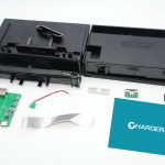
Take apart the output panel. The panel is fixed with snaps.

Crack open along the parting line, the top and bottom casing are assembled through the ultra-sonic welding process. We can see copper foil (touch sensor part) adhered at the top housing.

The PCB is fixed with screws.

Loosen the screws, PCB is taken away from the casing.
Prongs is engineered into modular type, with springs as the input conductor.
The battery is protected with black plastic insulation casing.

In addition to the protective casing, there are nano-material, and graphene materials used on the battery packs for enhanced safety purpose. The nano-material is used for heat insulation, while the graphene is to dissipate the heat on the battery pack. There are also mylars on both side of the battery pack for insulation purpose.

Battery cells are 21700 NCA Li-on cylindrical type, in serial connection.

The left side of the motherboard is the layout of AC adapter, with heat sink to help dissipation. The heat sink is wrapped with insulation tape.

The heat sink is soldered to PCB.

Removed the heat sink, we could see thermal pads placed on motherboard and daughterboard for heat dissipation.

Overview of the top side. Caps, transformers are applied with extra glue for fixation.
There is an insulation barrier that separates the primary and secondary sides.
The layout is very tightly fitted, with great volume efficiency.

According to the source, the product uses a special type of topology. Comparing to conventional topology which both of the DC to DC circuits have to operate simultaneously, this special type bypass one of the DC to DC circuit to improve efficiency.
In addition, there is an innovative mutual adjustment circuit used along with the bypass topology. This circuit could achieve DC to DC parallel powering through independent reference source without the need of any ICs.
The bypass topology has improved 3-4% efficiency comparing to conventional type. What's more stunning is, the whole circuitry of this topology is achieved through analog circuit (circled in red), without using any IC. This topology and circuit have already been applied for patent.

There is an LED soldered at the front end of the primary circuit. On the left is an inductor fit into the opening on the board.

Removed the daughterboard, we can see the caps and transformer below.

Fuse, X-Cap, filter caps, and so on are placed on motherboard. There are two boost inductors and two filter solid-state caps at the output side.

The fuse spec is 3.15A 250V.

X-cap, with insulation tube at the soldering pin.

Common mode inductor, for EMI filter purpose.

A pair of ABS210 rectifier bridges can even out heat.

All of the 3 high voltage filter caps are KCX series, manufactured by YMIN, 2 of which is 27uF 400V. These caps are released by YMIN in 2019 for GaN charger application. Its operating temperature range is between -55°C~105°C, with features of 3000hrs life-span, lightning proof, low current leakage (low standby energy consumption), high ripple current, high frequency low resistance, etc.
We have found out, YMIN KCX series caps are also used by Bull 65W GaN AC adapter, Philips 65W GaN power strip, Momax 65W 2C1A GaN AC adapter, UBI 30W 1A1C GaN AC adapter, Nubia 65W 2C1A GaN AC adapters, etc. It is a product with wide reputation.

The third one is 22uF, 400V.

I shape inductor, with heat shrink tube wrapped around.

The third filter cap is manufactured by Yunrui, the spec is 22uF, 400V.

Cap used for driver IC is 50V, 10uF.

Transformer close-up, with copper foil wrapped around for shielding purpose.

Controller IC, GaN MOS and Y-Cap are placed on the daughterboard.

There is another MOSFET and optocoupler at the other side of the daughterboard.

The controller driver chip is manufactured by ON-SEMI, model NCP1342, which is an HF-QR flyback primary side PWM controller with active X2 caps and multiple protection functions, and low standby power consumption.

High voltage GaN MOSFET is from Innoscience, model INN650D02, rated Vds 650W, max Vds at 750V, rated Rdson at only 0.2Ω. The MOSFET is complied with JEDEC standard application, features ESD protection, supports Kelvin Source. The max operating temperature can reach 150°C.
INN650D02 "InnoGaN" has excellent electrical characteristics, with very low Rdson, which is the perfect application on SMPS that requires high frequency and high efficiency. The size is DFN8*8, with excellent heat conductivity.
It is worthwhile to mention that INN650D02 uses 8-inch process, which was the first GaN component that went into mass production. And it is getting more and more popular in terms of application.

Detail spec of INN650D02

This is an HK1017 optocoupler, for primary-secondary feedback, on output voltage.

The SMD Y-Cap is from Sichuan TRX, which features small size, light weight, etc. It is the perfect match for high power density SMPS such as GaN AC adapter.

TRX specializes in passive component R&D, sales. The company register capital is at RMB 100 million.

This is a MOSFET, marked with 33477, for output ports controlling.

Another cap is soldered on the output PCB, and glued for extra fixation.

The heat sink and thermal pad at the back helps heat dissipation.

Removing the heatsink, we discover SR controller and SR MOSFET.

The synchronous rectifier controller comes from JoulVatt JW7726B, which supports CCM, DCM, QR and ACF modes and can effectively prevent the synchronous rectification MOSFET from turning on by mistake.

Specification of JoulVatt JW7726B.

Synchronous rectifier MOSFET is from Longten, model LSGN10R080, rated Vds at 100V, DFN5*6 in size.

Output filter solid cap is from YX electronic, rated at 220uF 25V.

The other output filter solid cap is from YX electronic as well, rated at 220uF 25V.

Close up on USB-C receptacle, with black tab, without showing metal.

Close up on the other USB-C receptacle

Back at motherboard, filter inductor, caps and thermistor are on the top side.

At the back of the motherboard is the buck-boost circuit, including two controller chips and two sets of eight MOSFETs.

The AC detection is realized through Hall components here.

Marked with 3016M.

The inductor in buck circuit of battery charging module. It is wrapped around the heat shrink tube.

Marked with 3346.

ZC micro-electronic, model ZCC6688T. It's a lithium battery charging IC.

Close up on the charging protection IC.

Touch sensor IC, marking 233DH.

The two unknown controller ICs, which markings are removed.

Here are 2 sets of MOSFET arrays, total of 8 pieces, model 3016M, for the purpose of buck-boost conversion, working along with controller IC.

Close up on the 2 inductors in buck-boost circuit.

Output solid state caps from YX electronic, rated at 220uF, 25V.

The other output solid caps from YX electronic, rated at 220uF, 25V.

Close up on thermistor.

Close up on the MOSFET by the Vbus, model 3345.

Close up on the other MOSFET by the Vbus, model 3347.

Close up on the illumination LED.

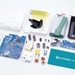
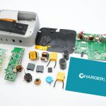
Full sets of parts and components.
Conclusion
The AC adapter with built-in battery pack from L Lab Corporation has glossy finished casing, properly-rounded corner and edge, which grip and touch are friendly for users.
The LED functions are very interesting, one is for capacity indication through touch, the other one is for emergency illumination.
Both USB-C ports support QC、AFC、FCP、PD protocol, configured from 5-20V, rated for 20-60W. It does the job of charging your laptop, and fast charging for 2 smartphones simultaneously, which is very functional.
The tech features, through the discovery of the teardown, are bypass topology and DC to DC parallel powering through independent reference sources. These features were unseen in our previous teardown.
And it uses quality components, controller IC from ON-SEMI, SR controller IC from JOULWATT, and HF MOSFET from Innoscience.
There are 2 controller chips to manage power bank, but unfortunately unidentified. The YMIN and YX caps help to reduce the dimension.
Also, there are very rounded protection features using thermistors, as well as heat conduction/insulation designs using heat sink and thermal pads.
In conclusion, the overall design and production process are well attended to.

