Introduction
This time, ChargerLAB got a 140W PD3.1 dual USB-C GaN charge from KOVOL. It is equipped with foldable US prongs for easy carrying. Both USB-C ports can support fast charging of 140W PD3.1 when used respectively. It also supports automatic power distribution.
Next, let's take it apart to see its internal components.
Product Appearance
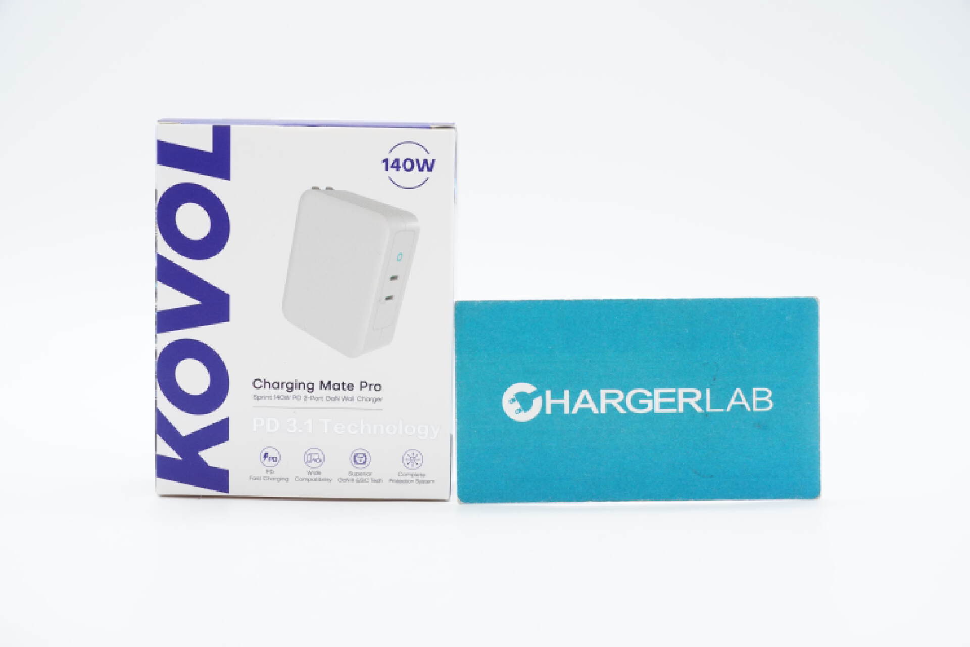
The "KOVOL", "140W", and four selling points are printed on the box.
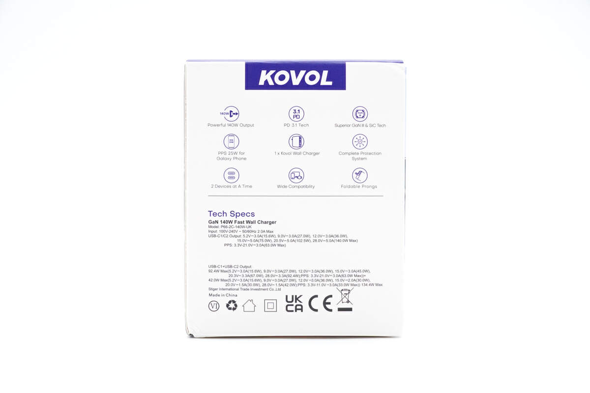
And the back has other selling points and specs info, which we'll talk about later.
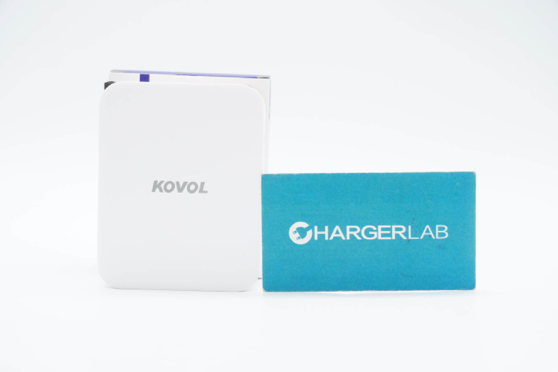
Take out the charger from the box.
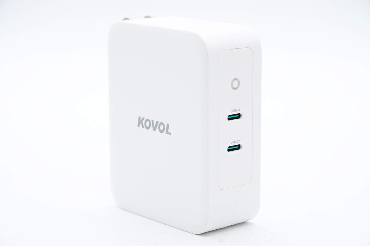
The white surface has a matte design.
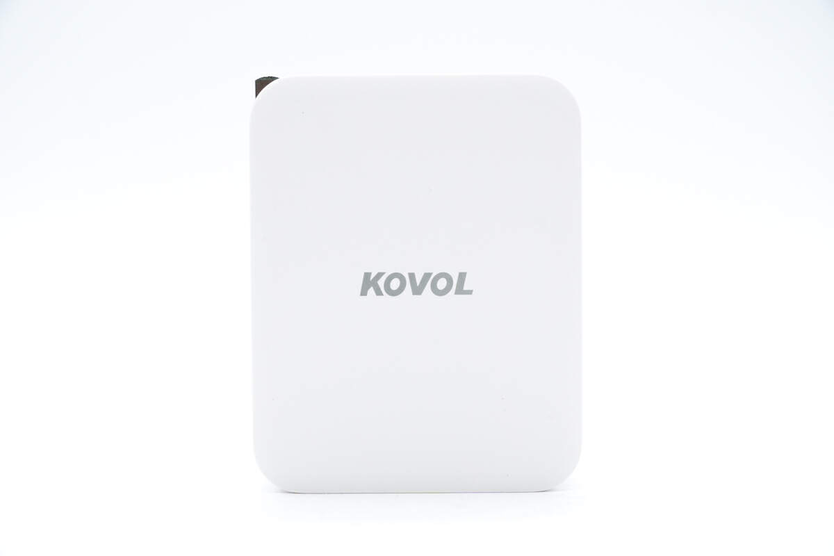
The "KOVOL" is printed on the front.
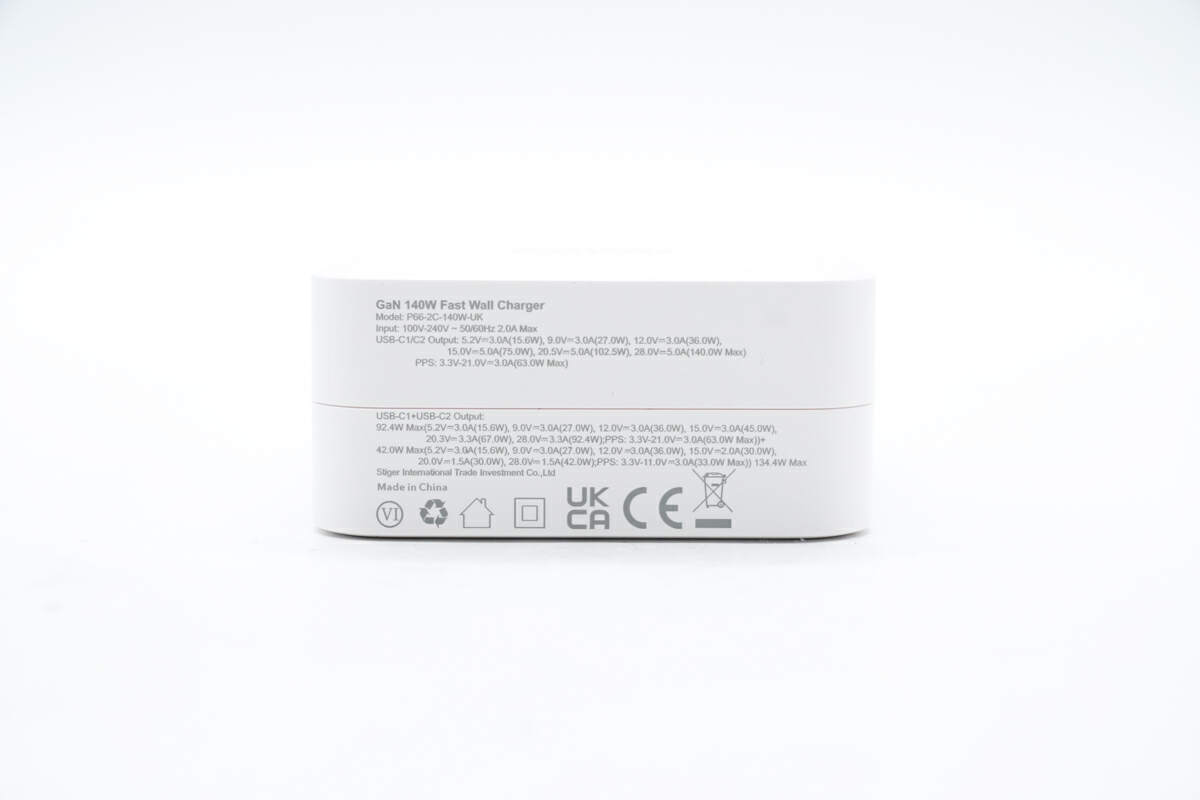
The specs info are printed on the bottom.
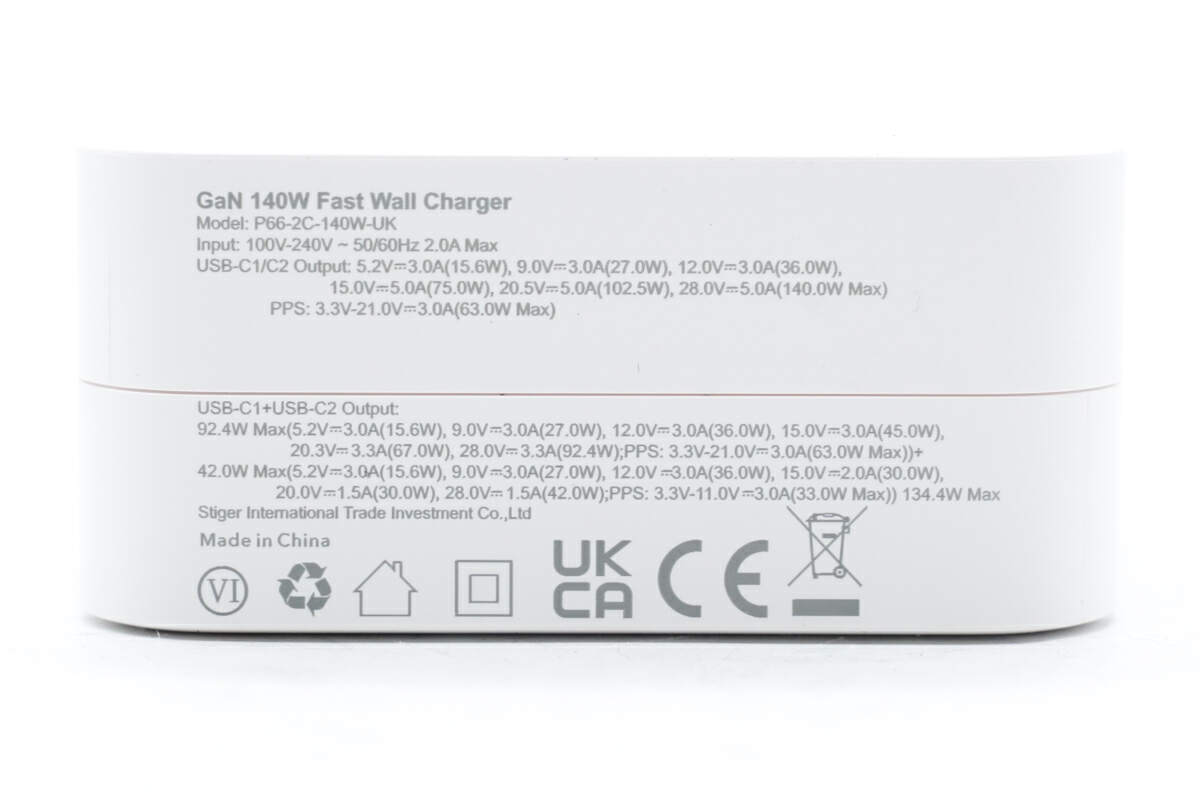
Model is P66-2C-140W-UK. It can support input of 100-240V~ 50/60Hz 2.0A. The maximum charging power of the USB-C1 and USB-C2 are 92.4W and 42W, respectively. The total output is 134.4W. It has passed CE, UKCA certifications, and VI-level energy efficiency certification.
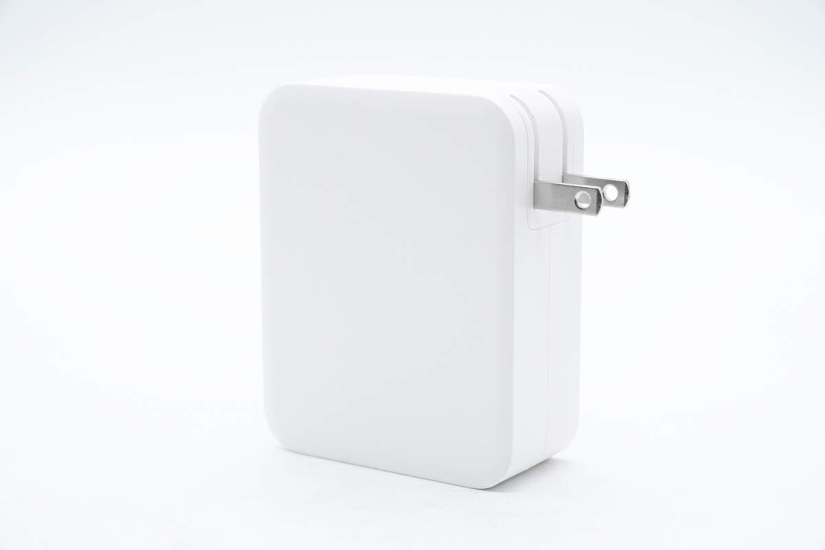
It comes with foldable US prongs.
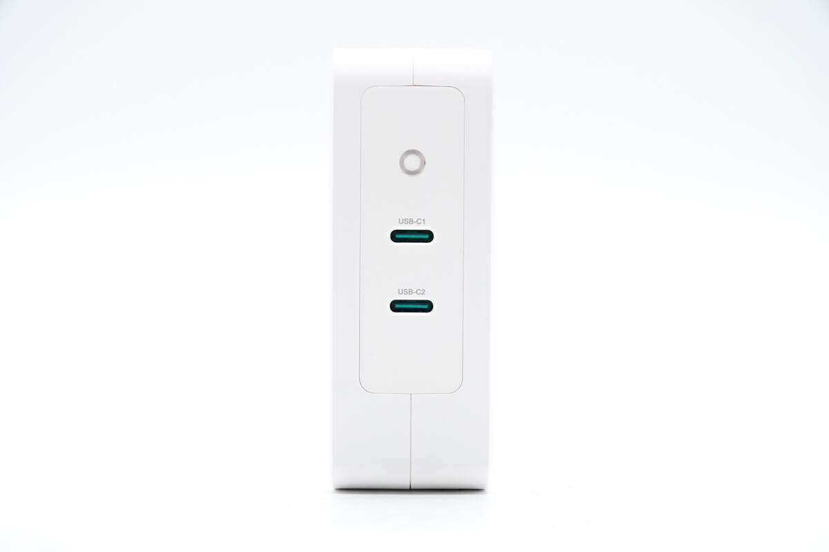
The output panel has a ring indicator and two green USB-C ports.
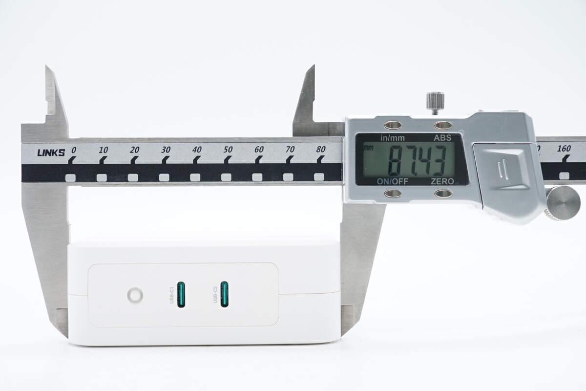
The length is about 87 mm (3.43 inches).
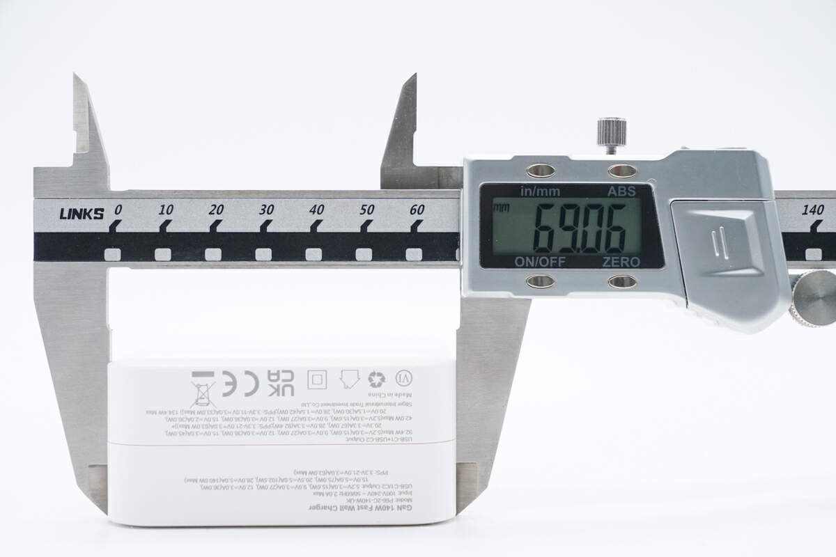
The width is about 69 mm (2.72 inches).
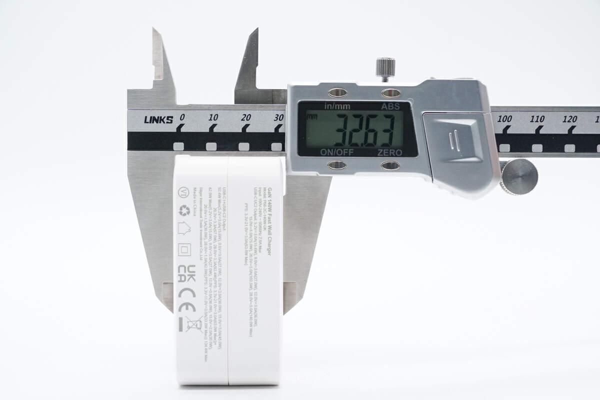
The thickness is about 33 mm (1.3 inches).
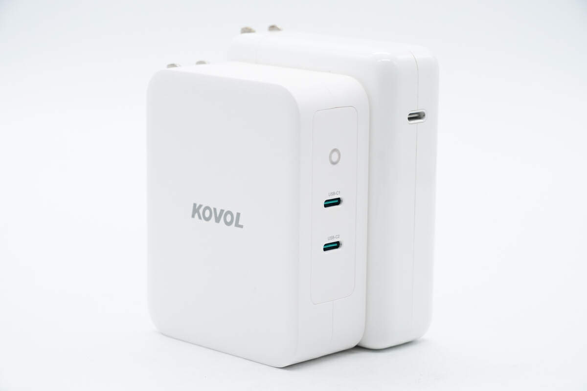
It is smaller than the Apple 140W charger.
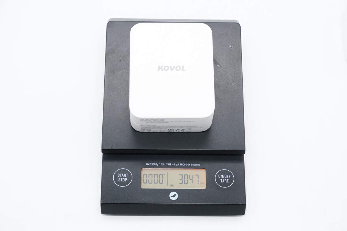
And the weight is about 305 g (10.76 oz).
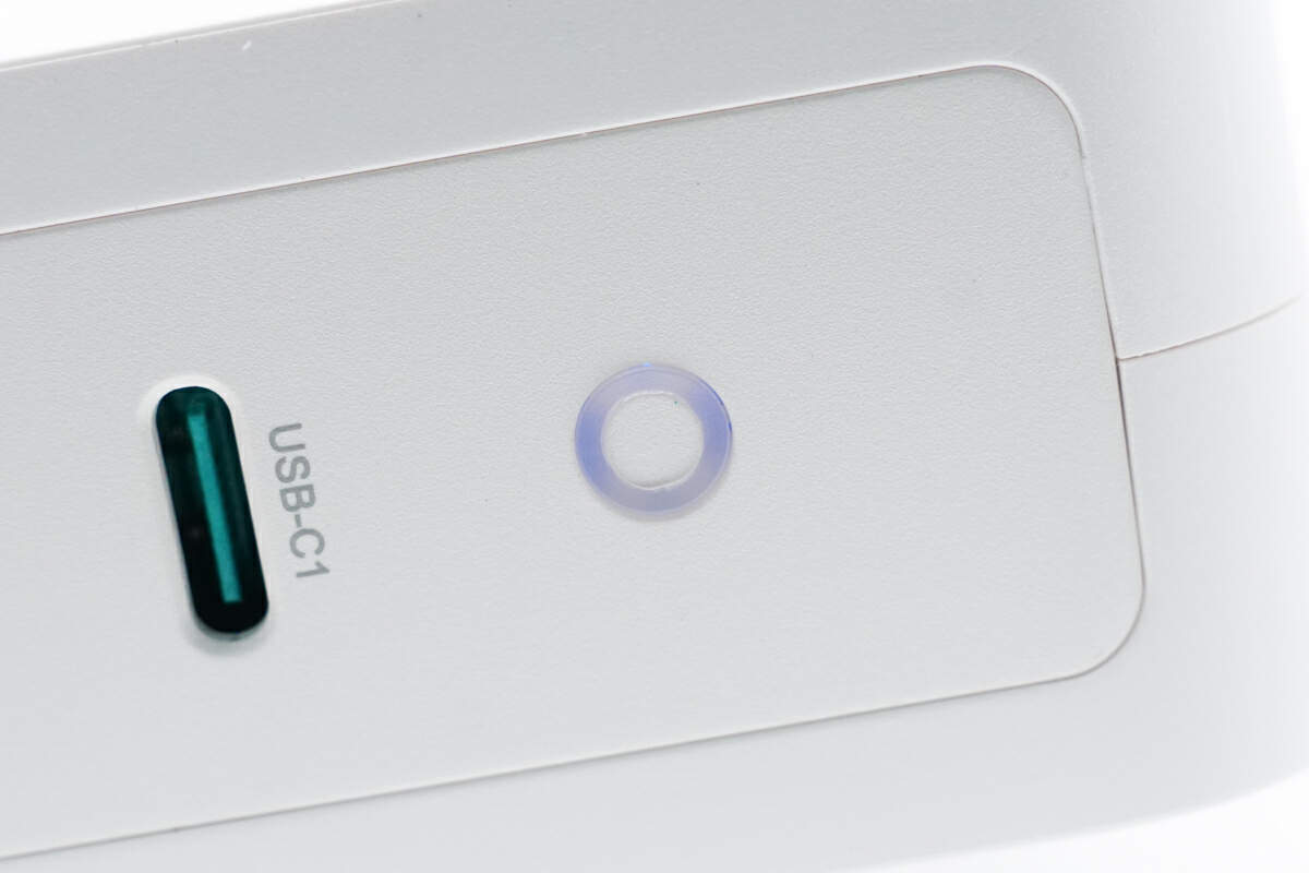
The indicator lights up blue when powered on.
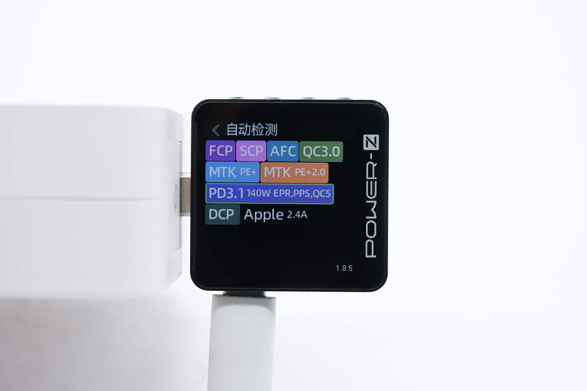
The ChargerLAB POWER-Z KM003C shows that the USB-C1 supports FCP, SCP, AFC, QC3.0/5, PE2.0, PD3.1, PPS, DCP, and Apple 2.4A protocols.
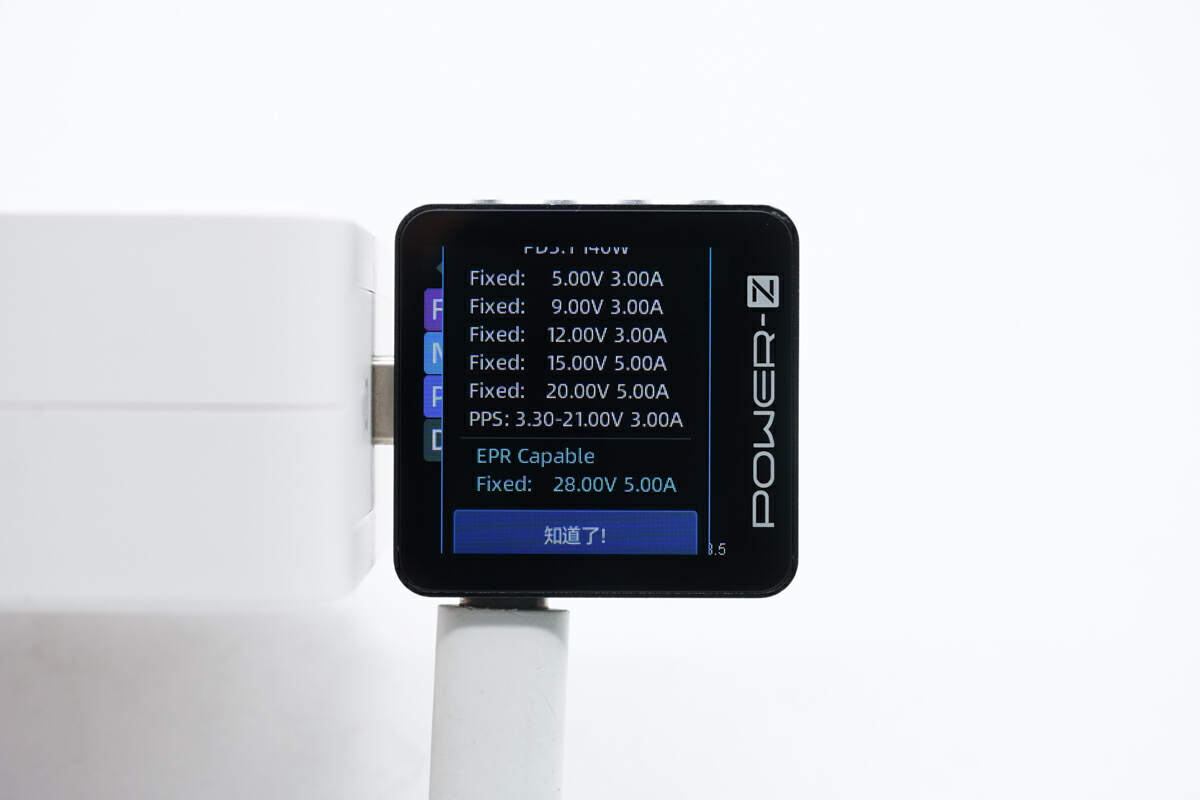
And it has six fixed PDOs of 5V3A, 9V3A, 12V3A, 15V5A, 20V5A, and 28V5A, and a set of PPS, which is 3.3-21V3A.
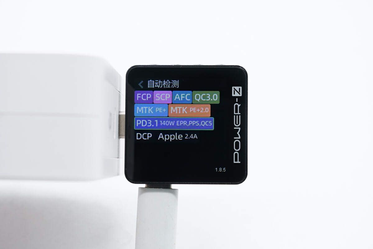
The supported protocols of USB-C2 are the same as the USB-C1.
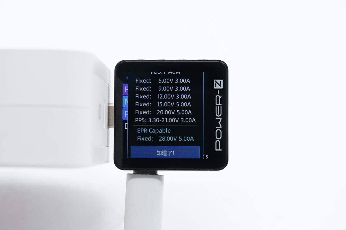
So are the PDOs.
Teardown
Now, let's start to take it apart.
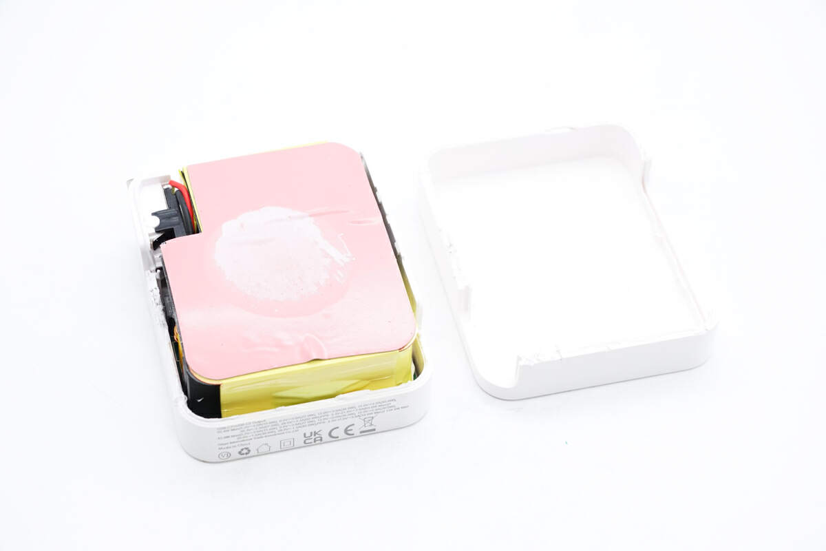
Take out the cover, there is a pink thermal pad on the PCBA module.
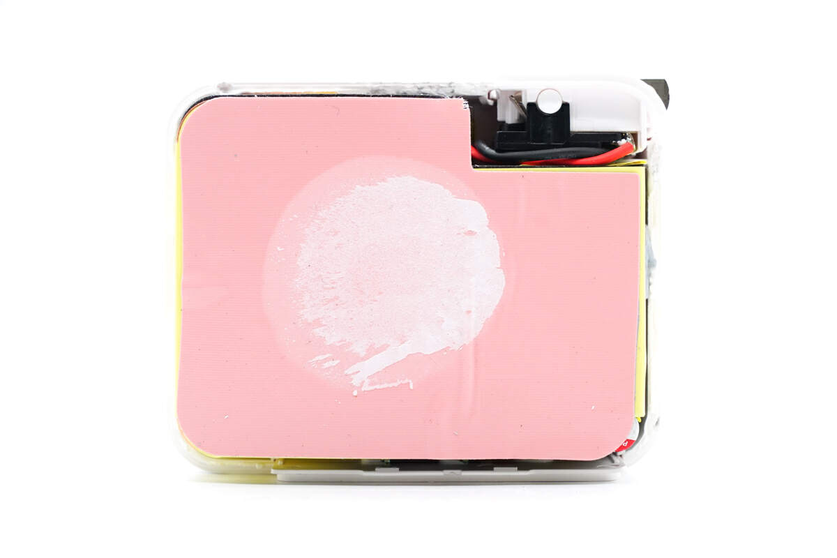
The thermal pad is fixed with glue.
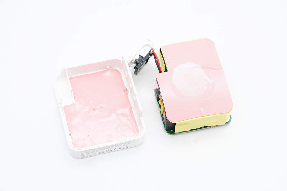
There are also thermal pads on the other side.
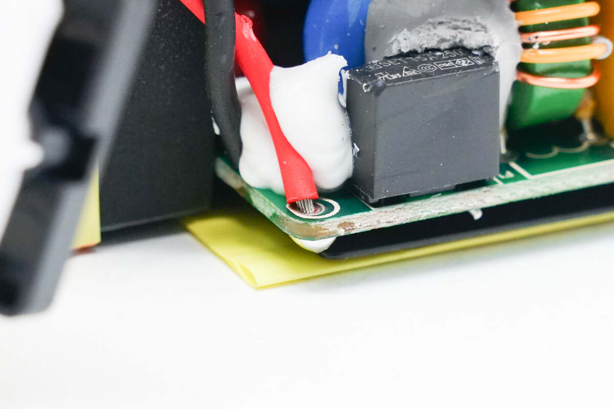
The foldable prongs are soldered to the PCBA module via wires.
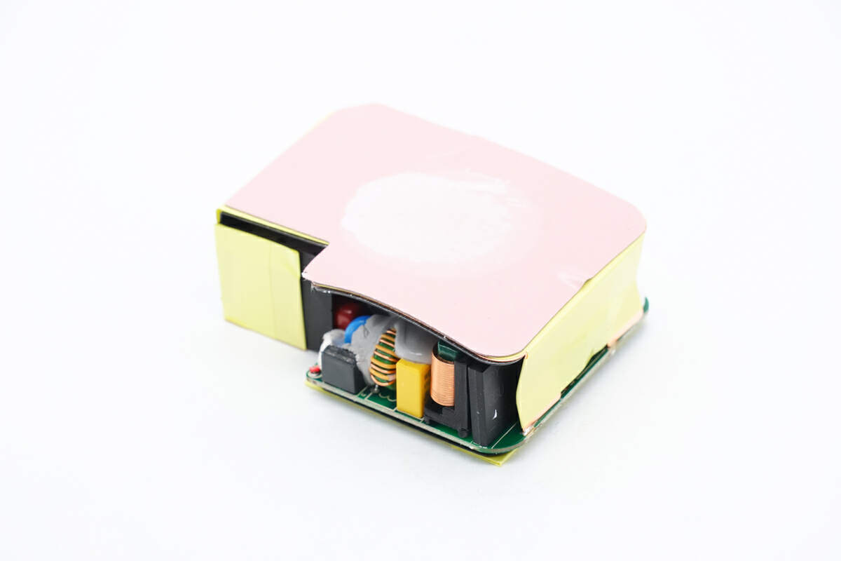
It also has copper sheets to enhance heat dissipation.
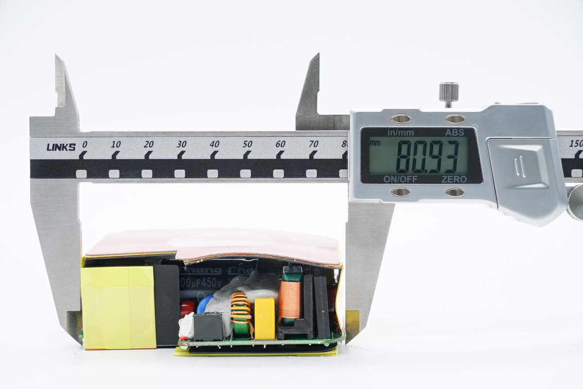
The length of the PCBA module is about 81 mm (3.19 inches).
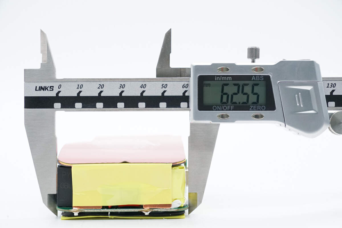
The width is about 63 mm (2.48 inches).
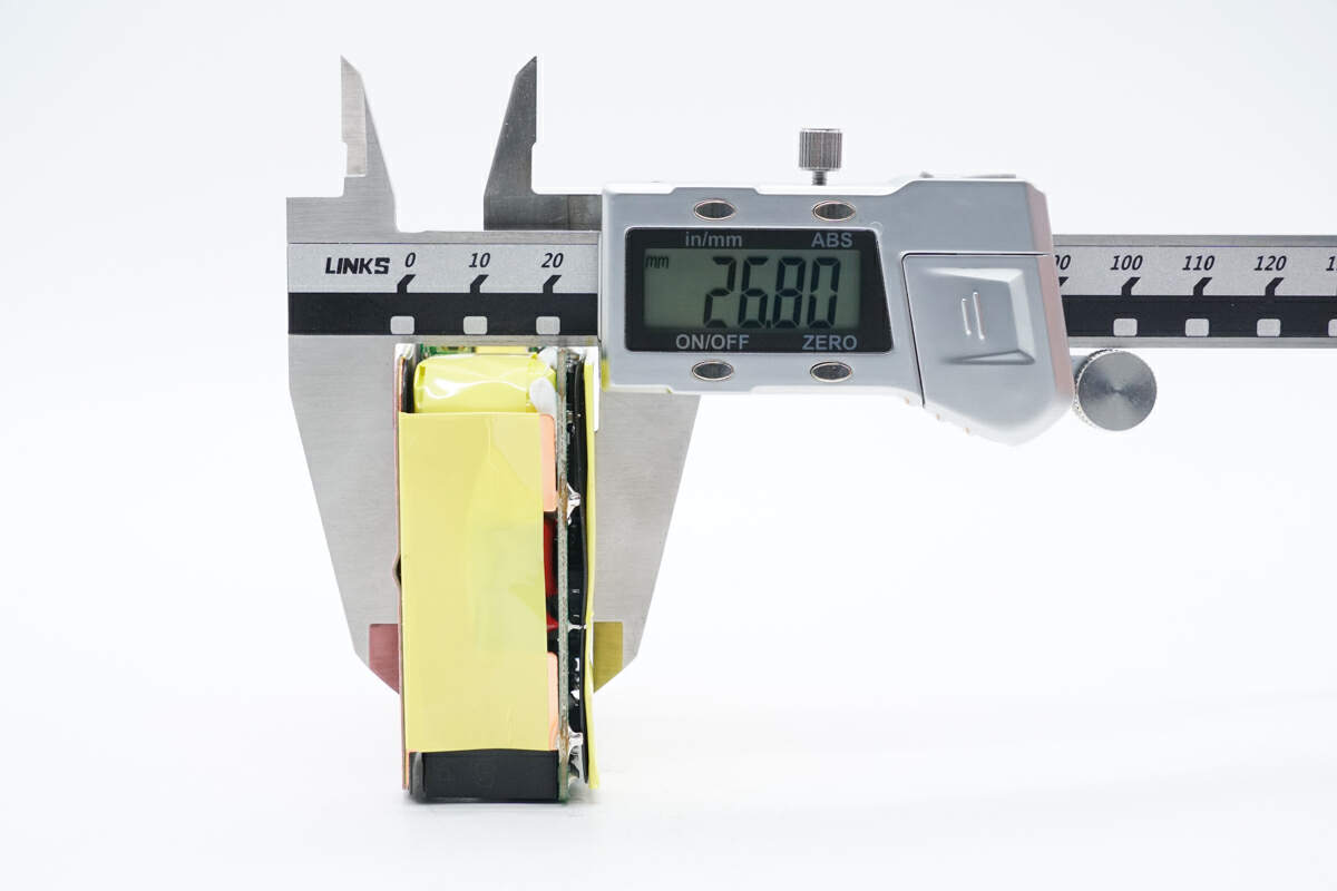
The thickness is about 27 mm (1.06 inches).
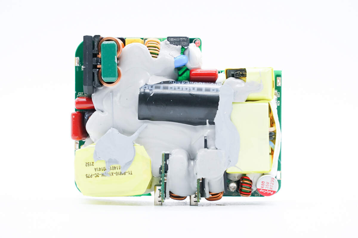
Remove the heat sinks and all the gaps between the components are filled with potting compound for fixing and heat dissipation.
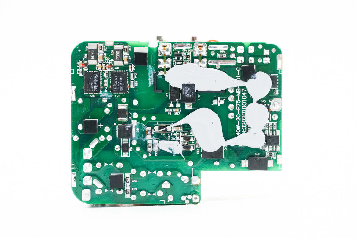
The MOSFETs and synchronous rectifier are also covered with potting compound for heat dissipation.
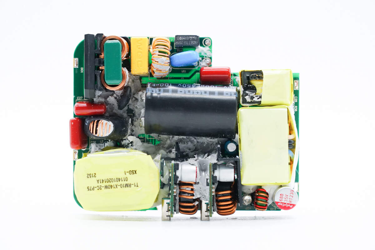
There are fuse, common mode choke, safety X2 capacitor, bridge rectifier, NTC thermistor, and inductor on the front.
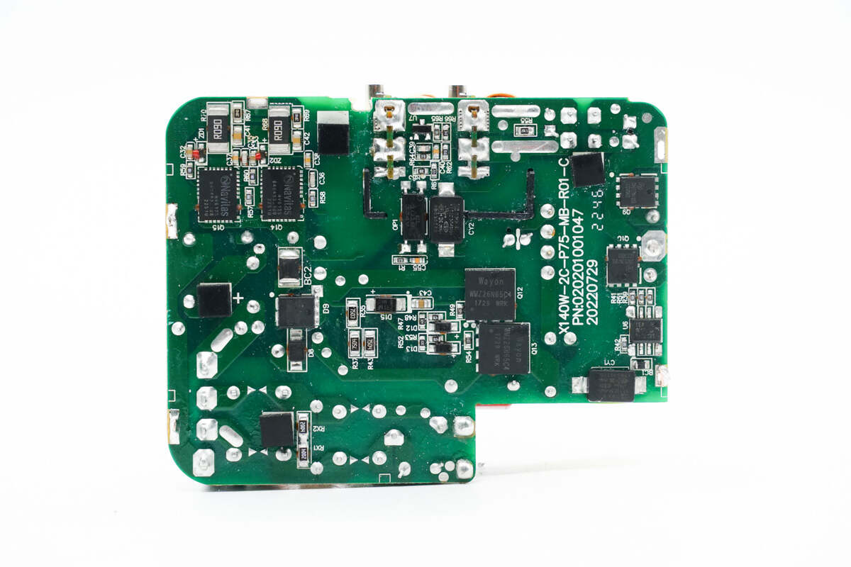
The master control chip, feedback optocoupler, SMD Y capacitor, and synchronous rectifier controller are on the back.
ChargerLAB found it adopts a PFC circuit and LLC topology with fixed output voltage. And it has two independent buck circuits.
Next, we will take a look at each component starting from the input end.
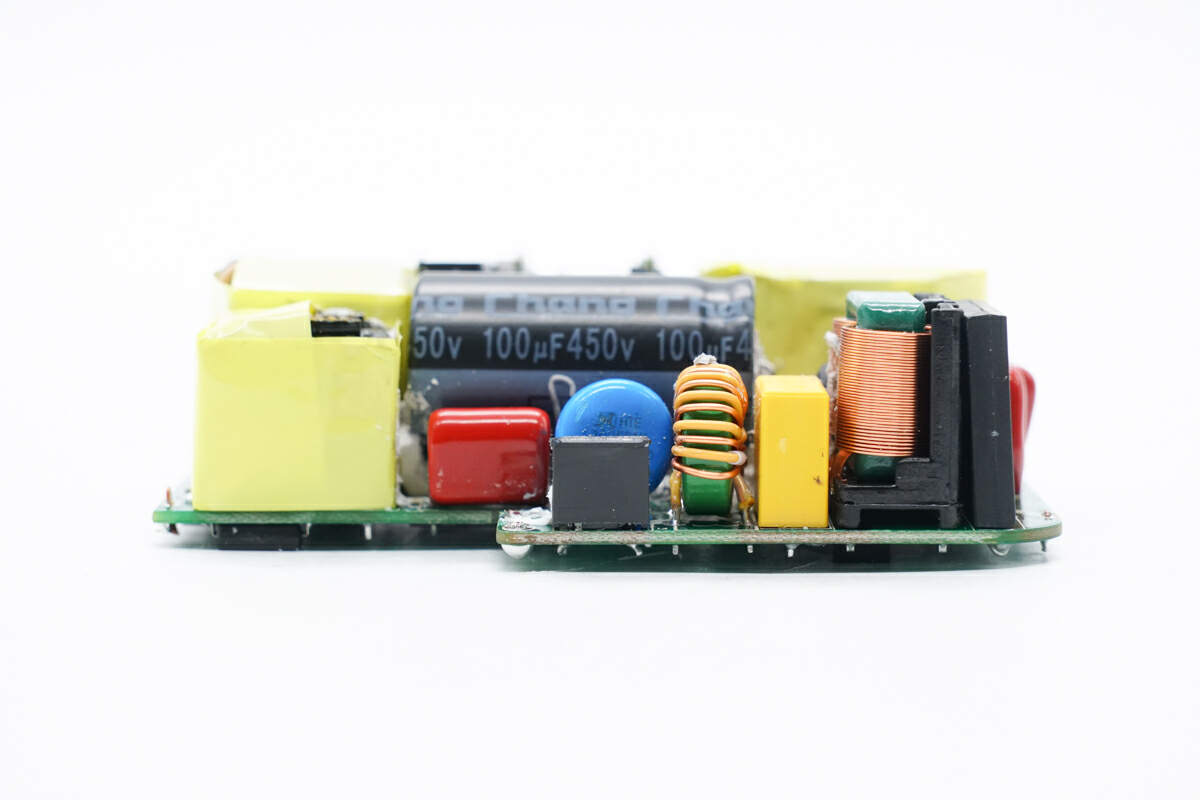
There are LLC transformer, fuse, common mode choke, safety X2 capacitor, and bridge rectifier on the side of the PCBA.
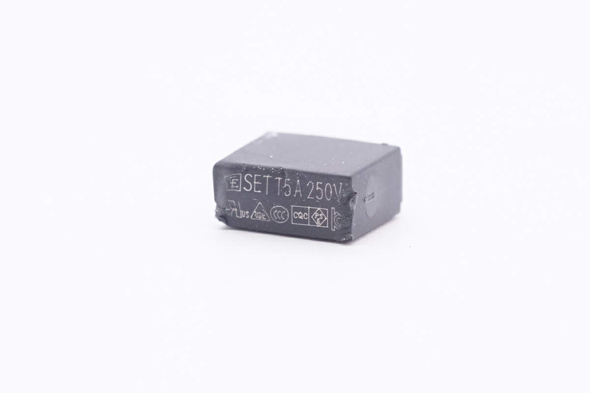
The input fuse is from Chevron. 5A 250V.
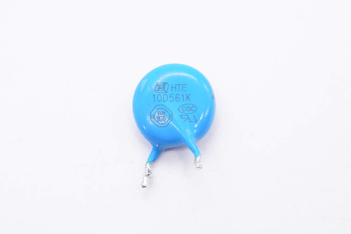
The varistor is used to suppress the surge current when powering on. Model is HTE10D561K.
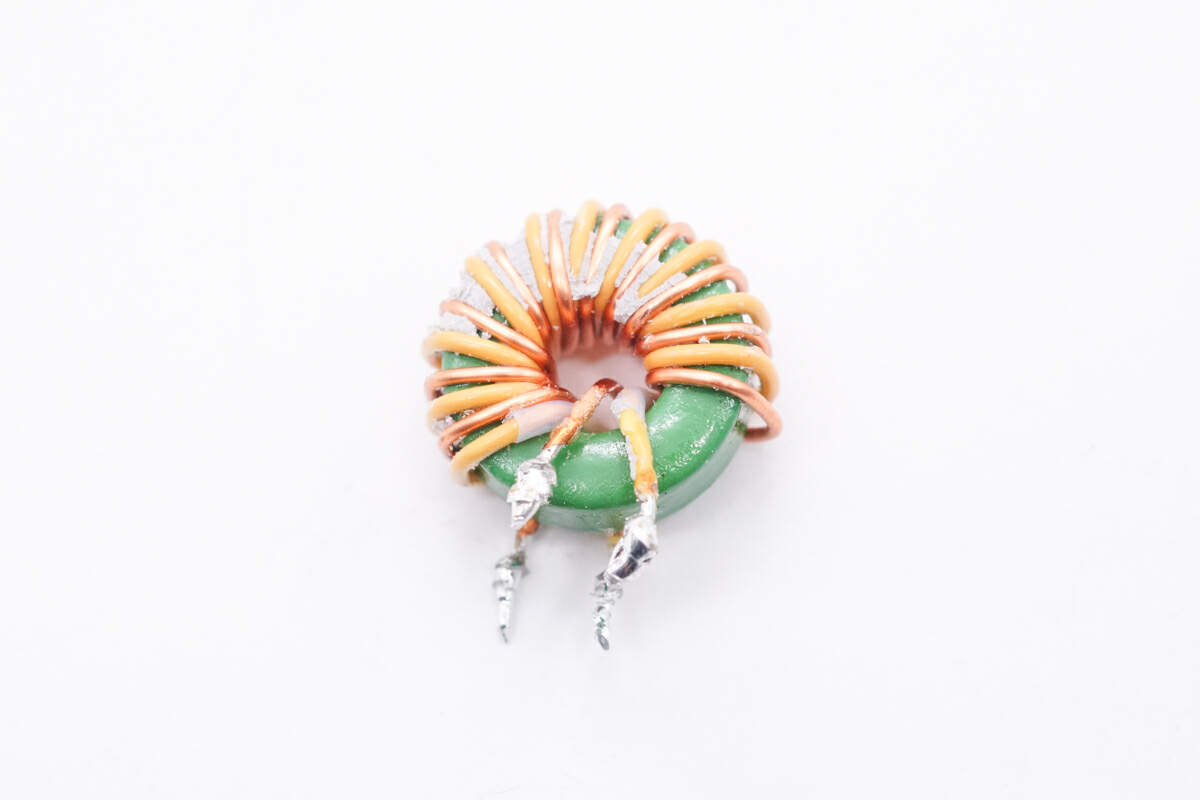
The common mode choke is wound with magnet and insulated wires.
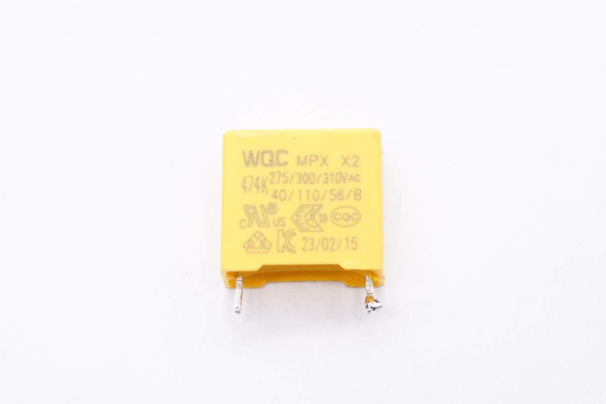
The safety X2 capacitor is from WQC. 0.47μF.
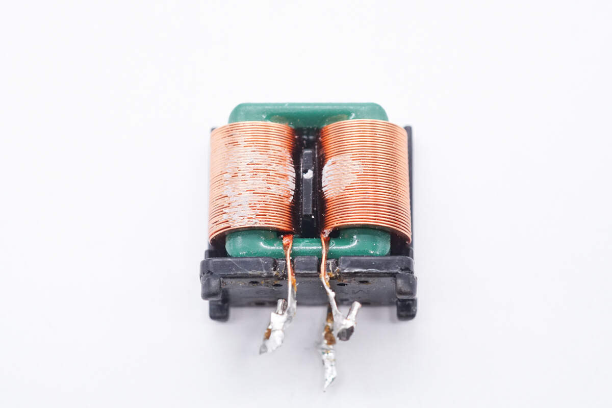
The second common mode choke is wound with flat copper wires.
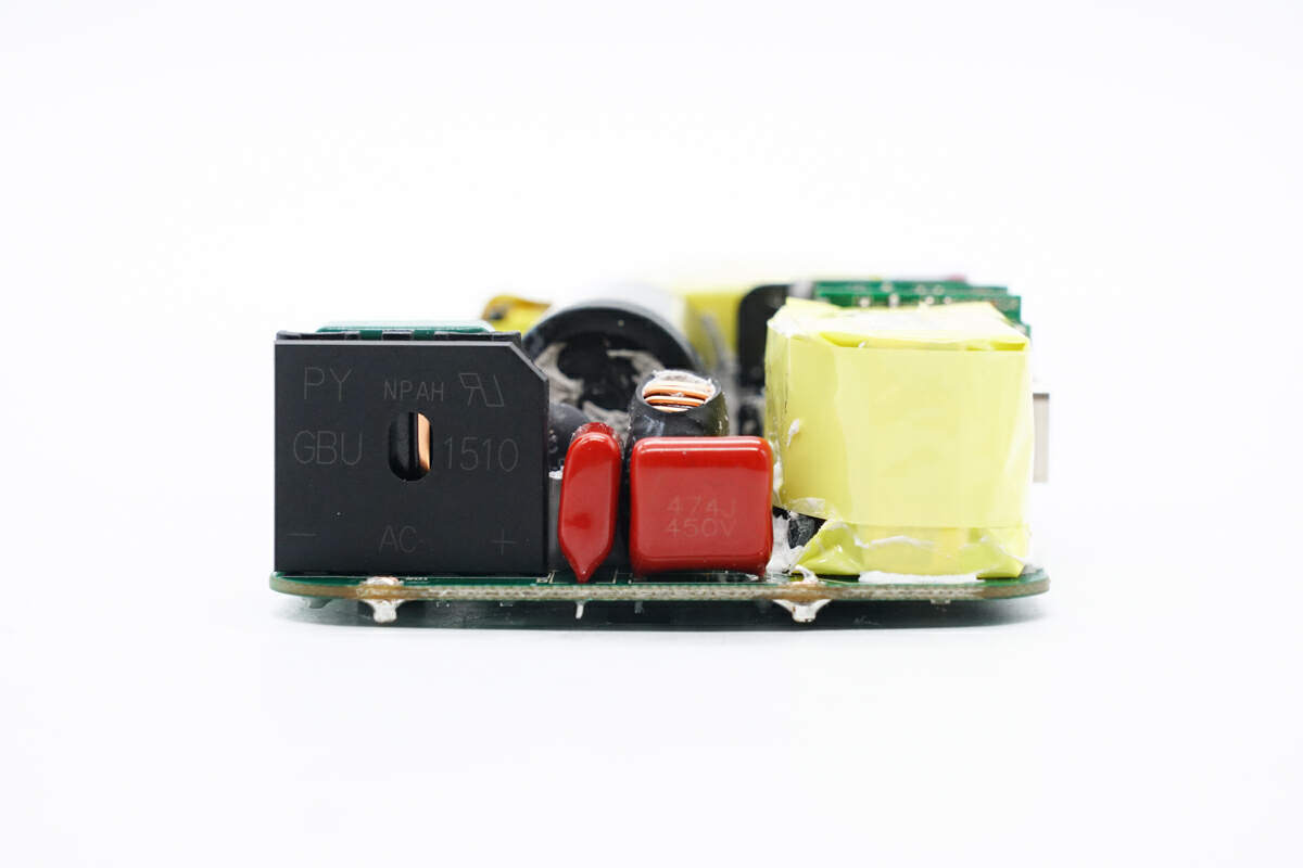
The other side has the bridge rectifier, film filter capacitor, and PFC boost inductor.
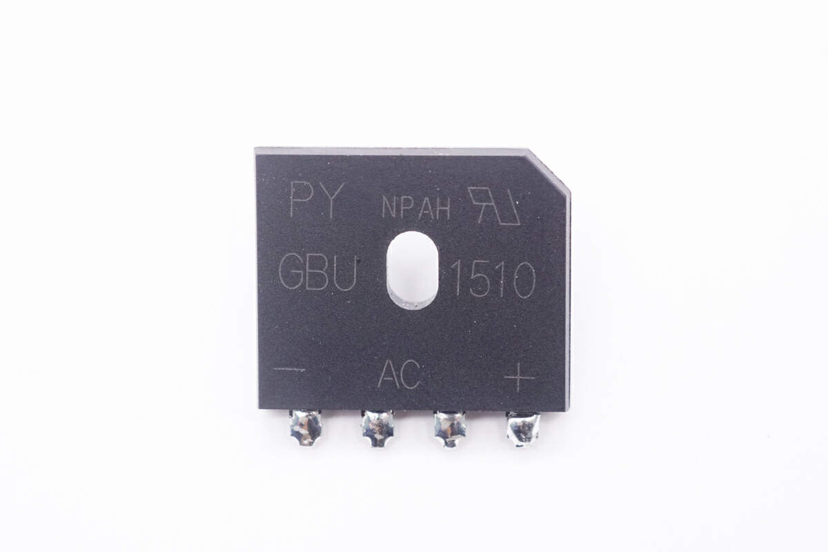
The bridge rectifier is from Pingwei. Model is GBU1510. 15A 1000V.
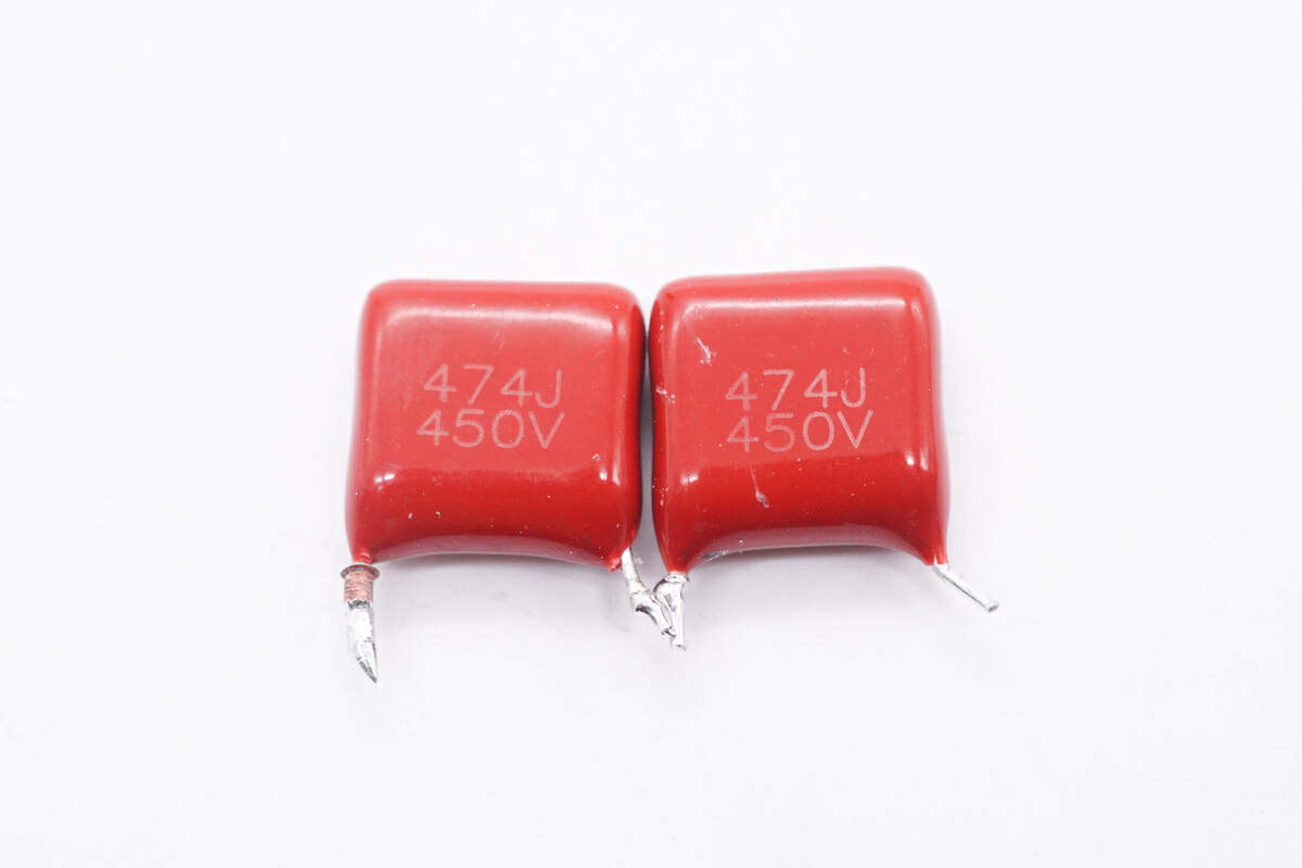
The specifications of these two film filter capacitors are 0.47μF 450V.
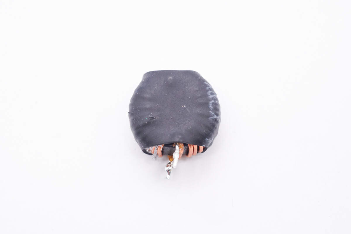
The filter inductor is wounded with magnetic ring and insulated by heat-shrinkable tubing.
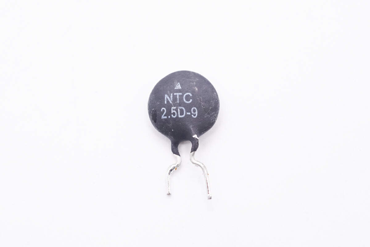
The NTC thermistor is used to suppress the surge current when powering on.
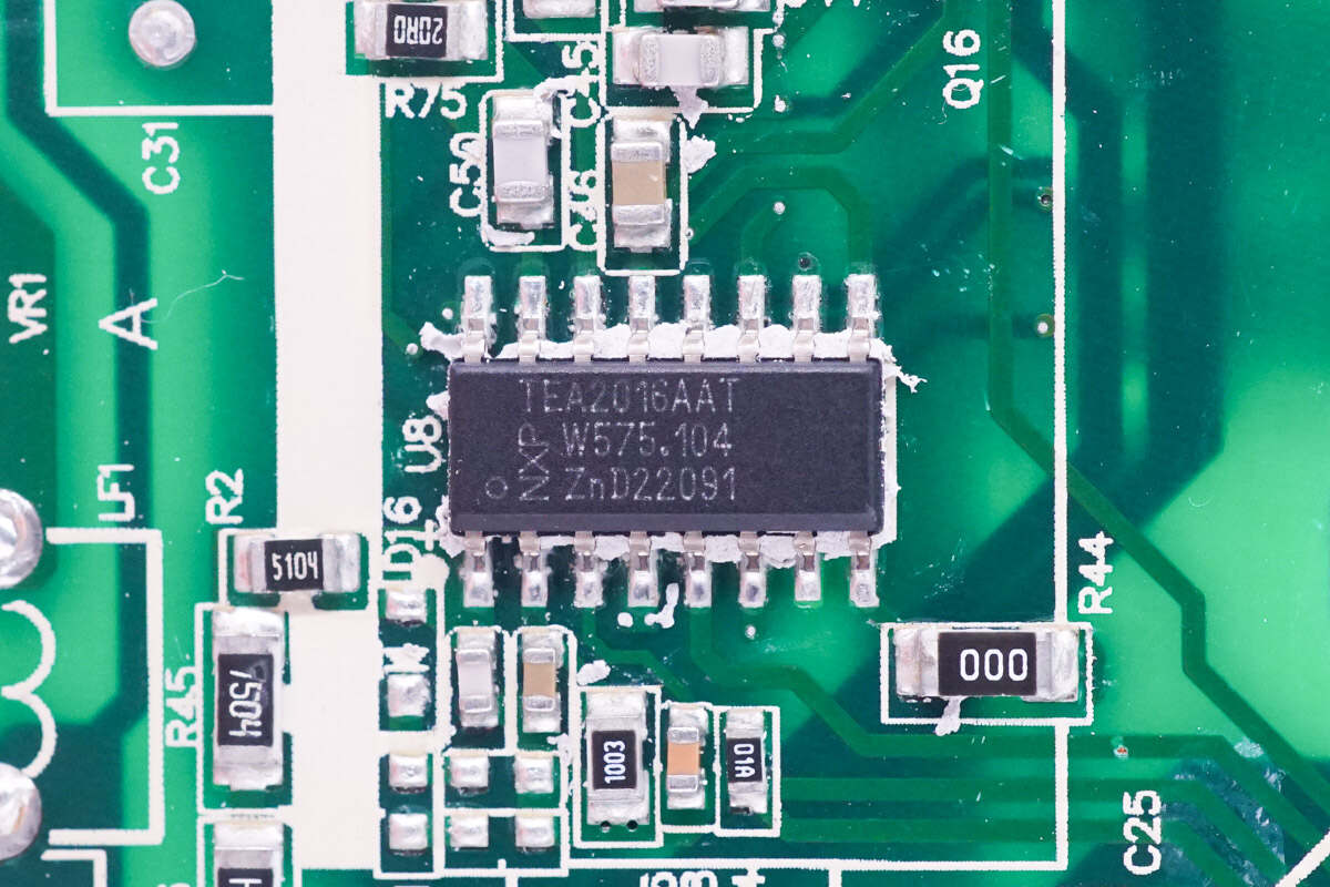
The master control chip is from NXP. It integrates LLC and PFC controller. Model is TEA2016AAT.
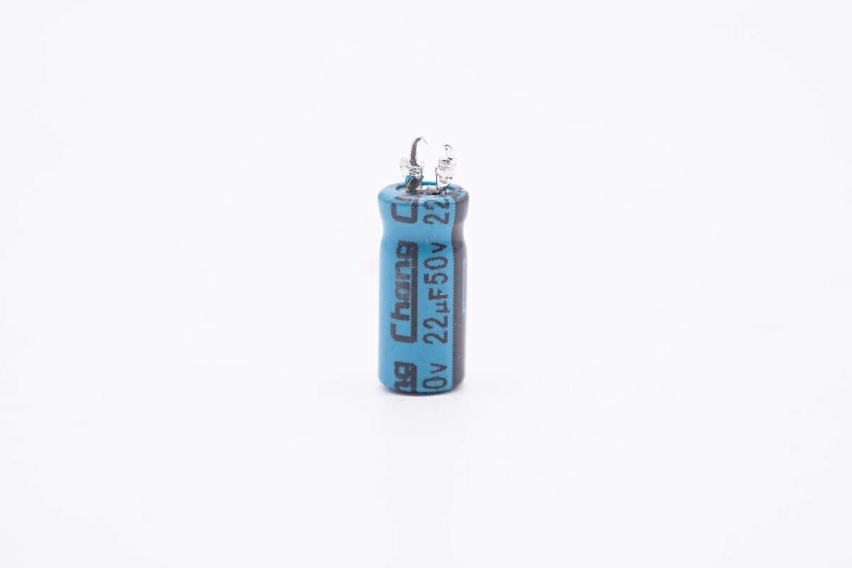
The electrolytic capacitor that powers the master control chip is from HWE. 22μF 50V.
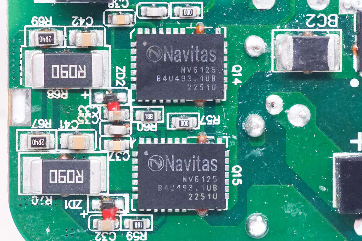
These two GaN FETs are from Navitas and adopt QFN6 x 8mm pacakge. They integrate drivers and support a switching frequency of 2MHz. Model is NV6125. 175mΩ 650V.
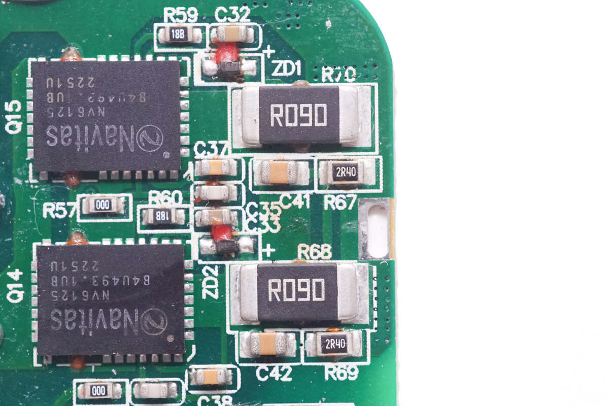
Two sampling resistors are used to detect the current of MOSFETs. 90mΩ.
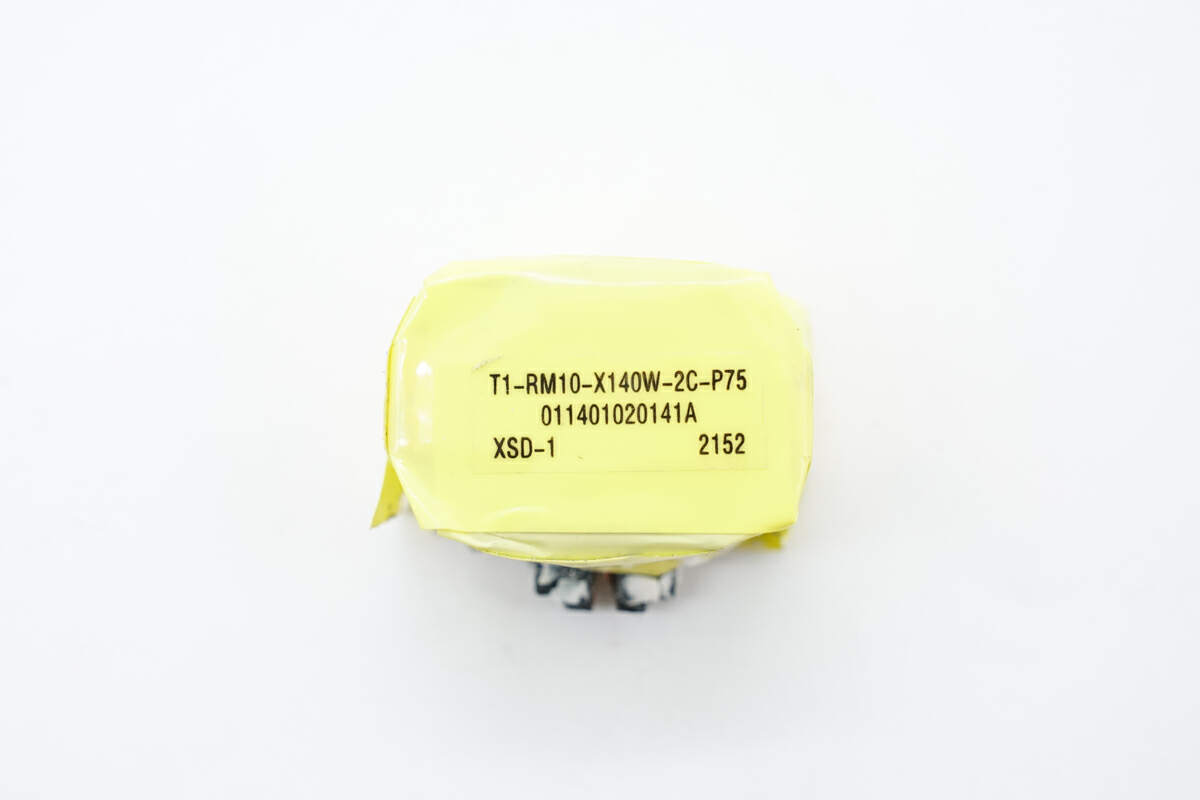
The PFC boost inductor is wound with RM10 magnetic core. And the magnetic core is insulated by tape.
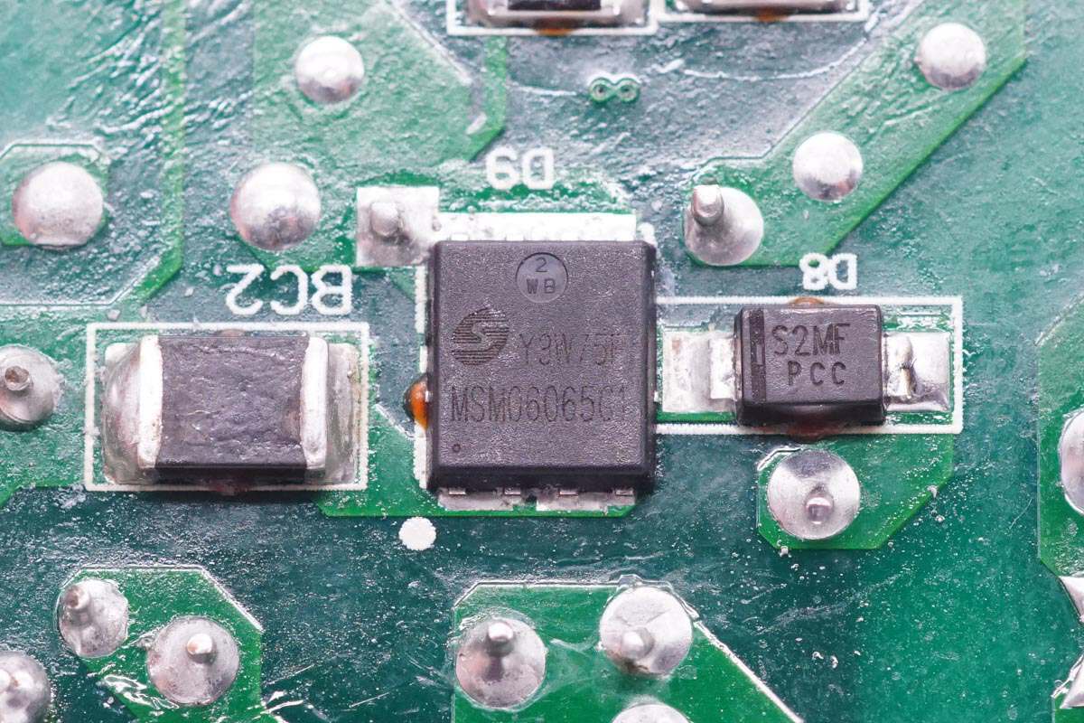
The PFC SiC rectifier is from Maplesemi and adopts DFN5 x 6 package. It can support a continuous positive current at 150℃. Model is MSM06065G1. 650V 6A.
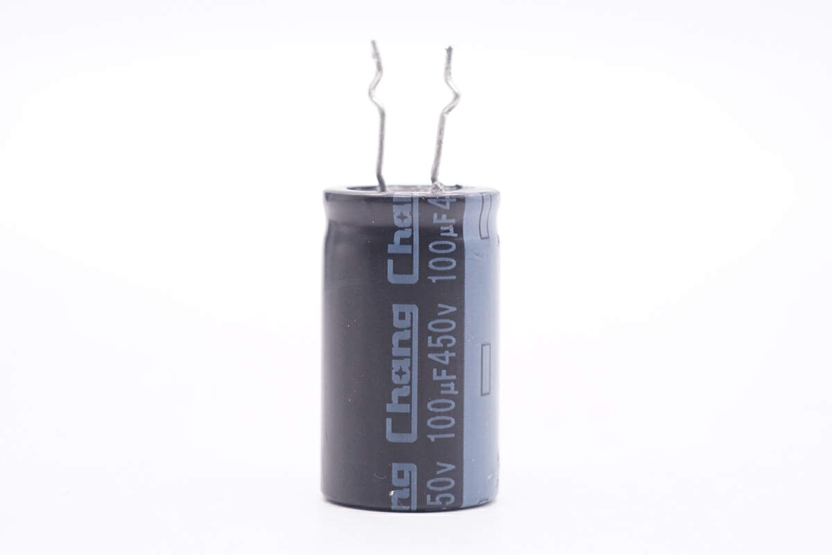
The electrolytic capacitor is also from HWE. 100μF 450V.
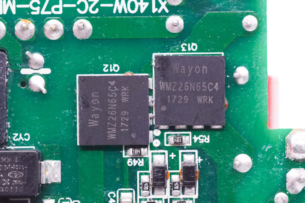
These two LLC MOSFETs are from WAYON and adopt DFN8 x 8 pacakge. Model is WMZ26N65C4. 650V 160mΩ.
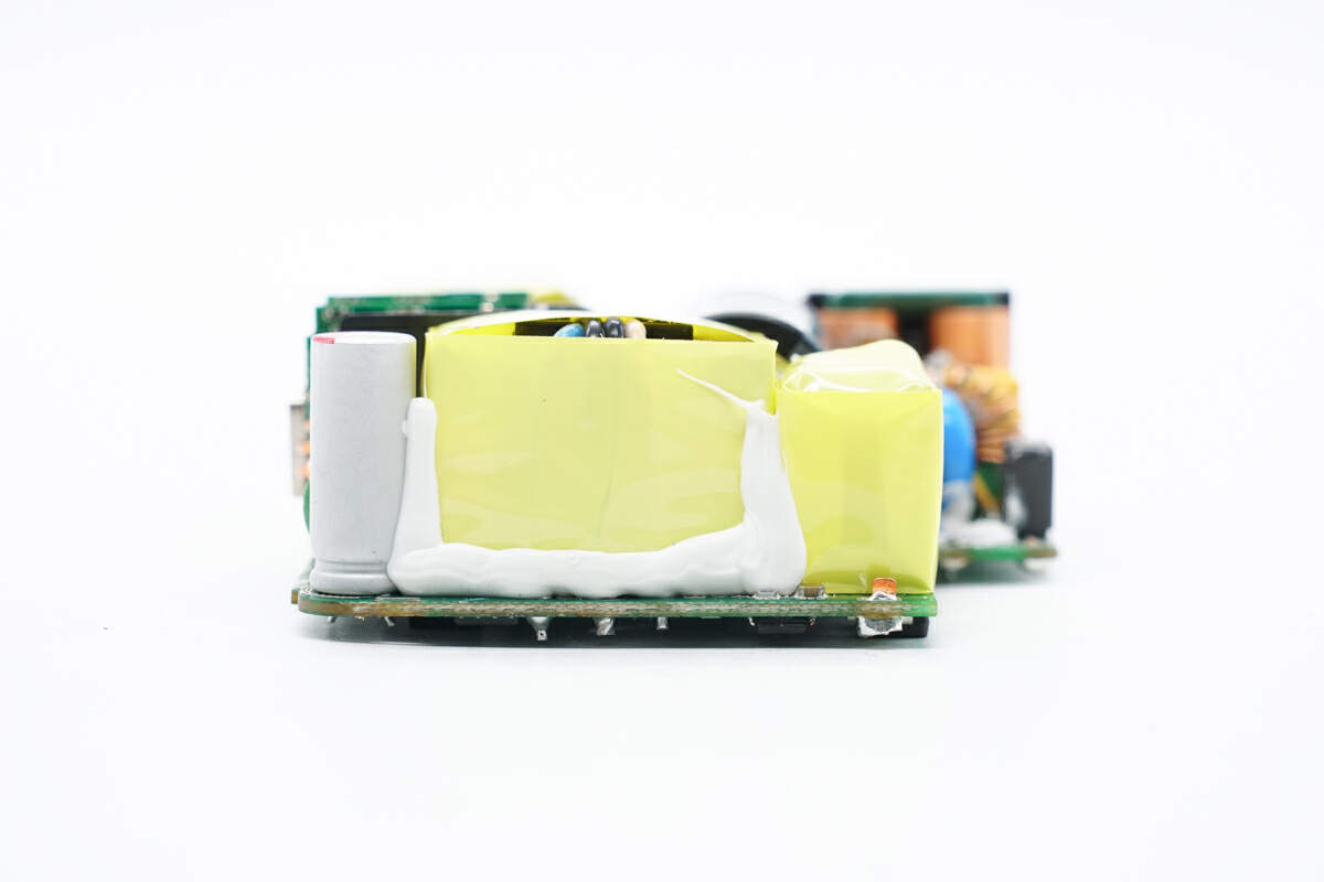
There are resonant inductor, transformer, and filter capacitor on this side of the PCBA module. The transformer is fixed with glue.
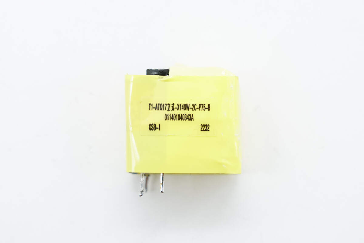
The magnetic core of the resonant inductor is insulated by tape.
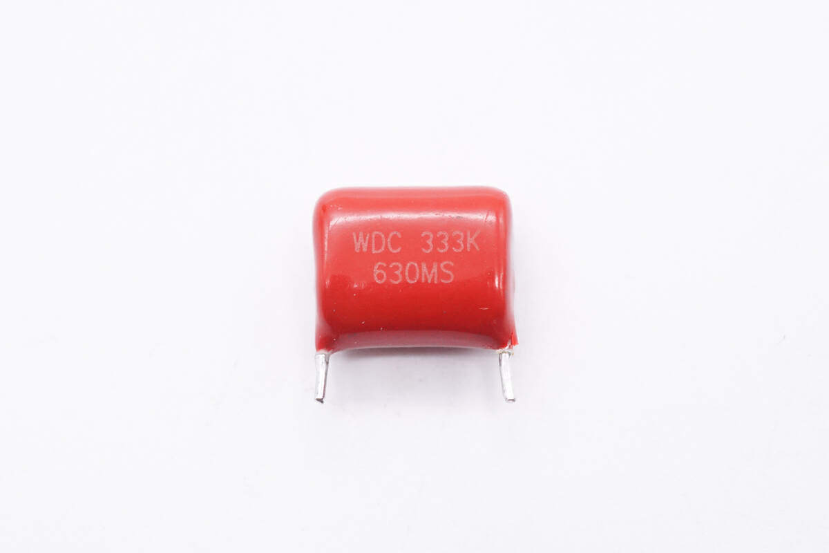
The resonant capacitor is from WDC. 0.033μF 630V.
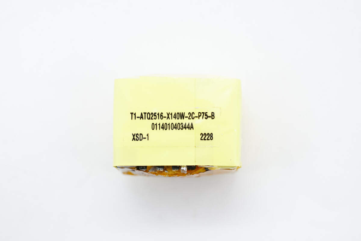
The LLC transformer is wounded with ATQ2516 magnetic core and insulated by tape.
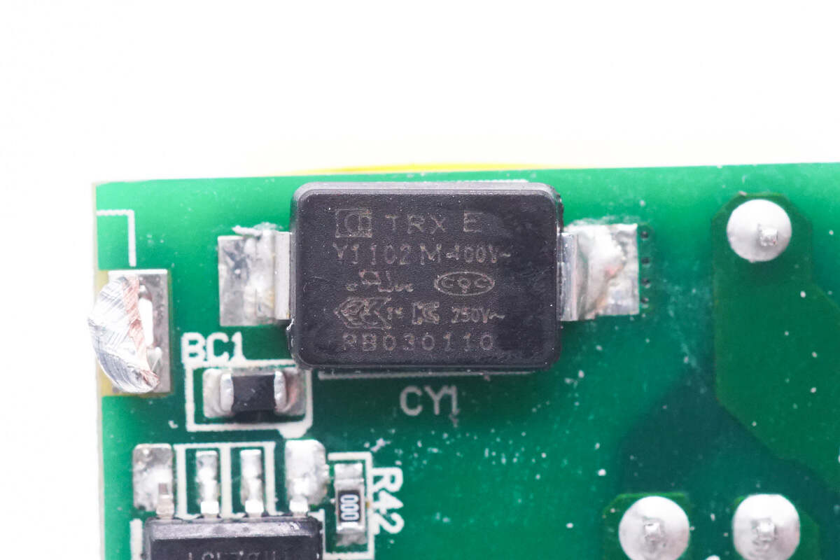
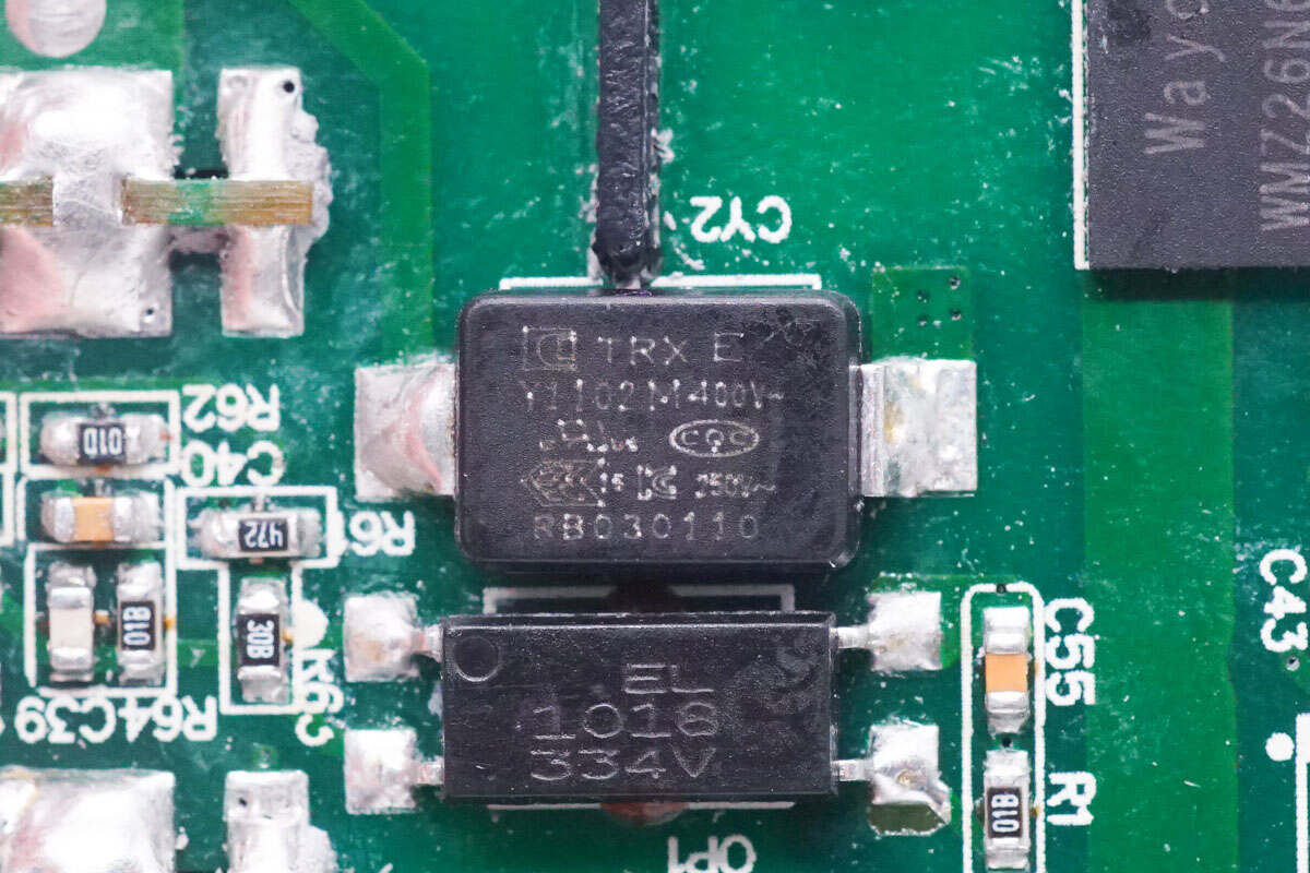
The SMD Y capacitor is from TRX. Its small size and light weight are suitable for high-density power products such as GaN fast chargers. Model is TMY1102M.
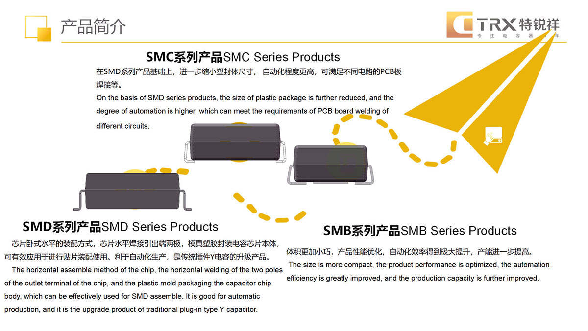
Here are some information about TRX products.
The other SMD Y capacitor has the same model as the previous one.
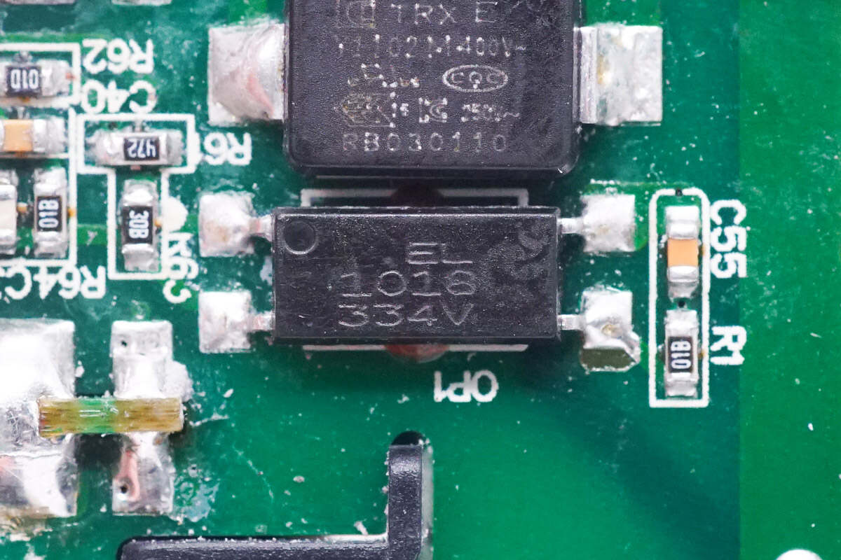
The optocoupler marked with EL1018 is from Everlight. It is used for output voltage feedback.
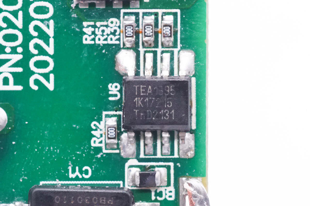
The synchronous rectifier controller is from NXP. It can support voltage of 38V, far beyond the 28V output requirement of USB PD3.1. Model is TEA1995.
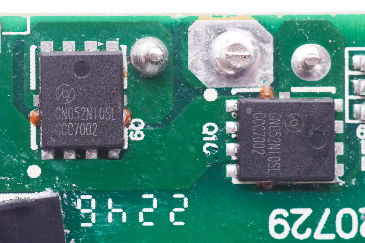
The synchronous rectifier is from Hunteck and adopts DFN5 x 6 pacakge. Model is HGN052N10SL. 100V 4.6mΩ.
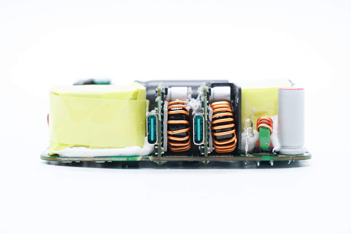
There are two buck PCBs on the output end.
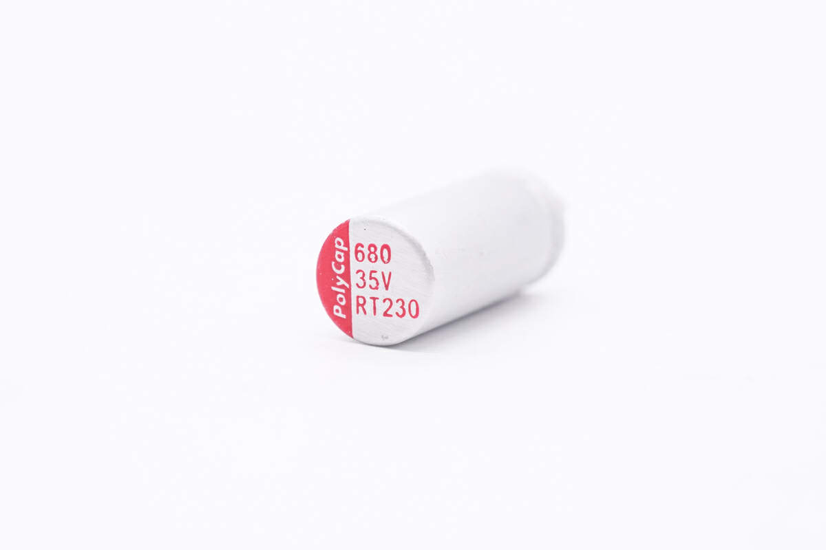
The solid capacitor for output filtering is from PolyCap RT series. 680μF 35V.
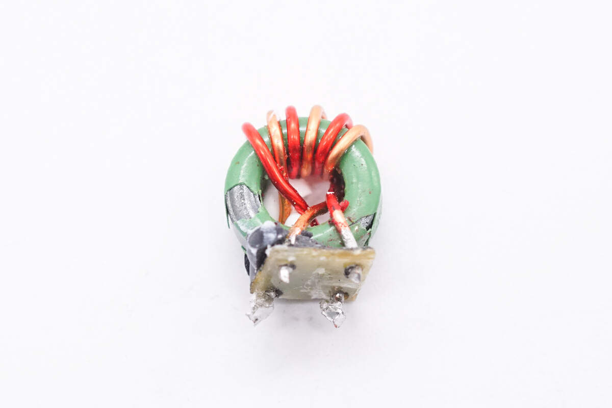
The output filter inductor is wound with magnet ring, and insulated with bakelite.
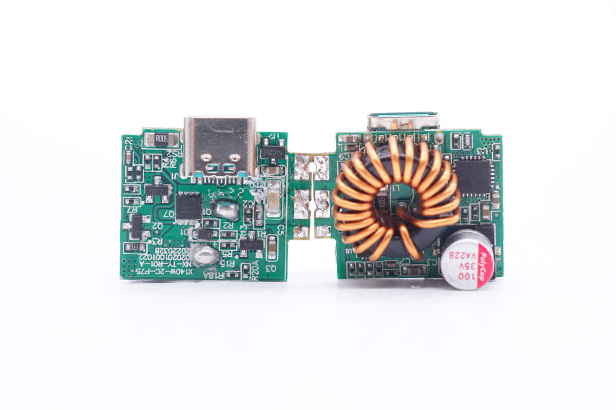
The specifications of the two output ports and the two buck PCBs are exactly the same. So we choose one of them to introduce.
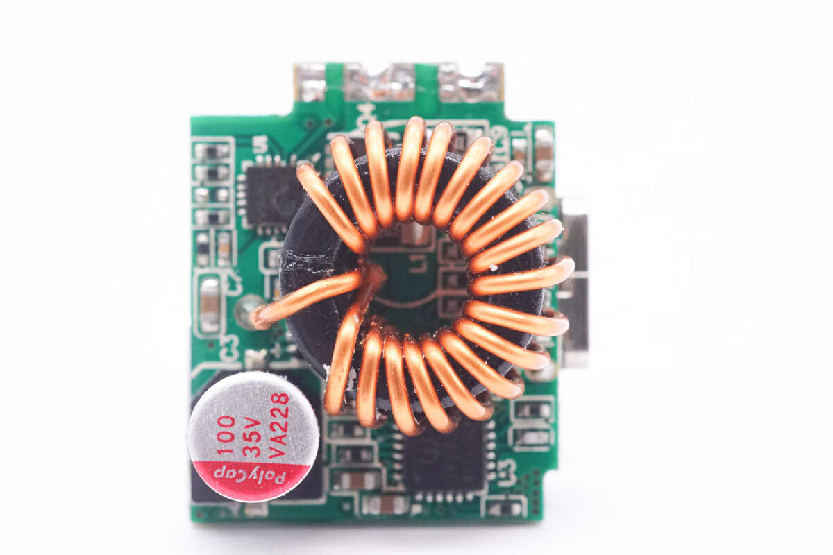
There are buck inductor, MOSFET, protocol chip, synchronous buck controller, and capacitor on the front.
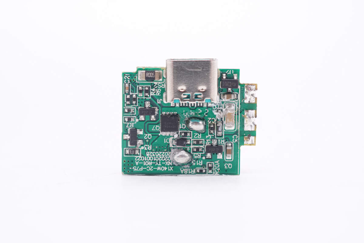
The VBUS MOSFET, sampling resistor, and USB-C socket are on the back.
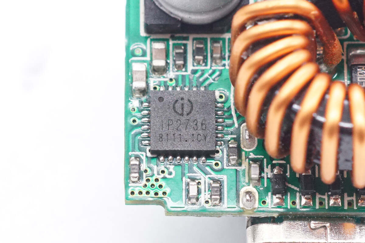
The protocol chip is from Injoinic. It Integrates programmable voltage/current loop control, and current detection. It supports loss compensation of output, feedback, and changes the output voltage by I2C and FB control. Model is IP2736.
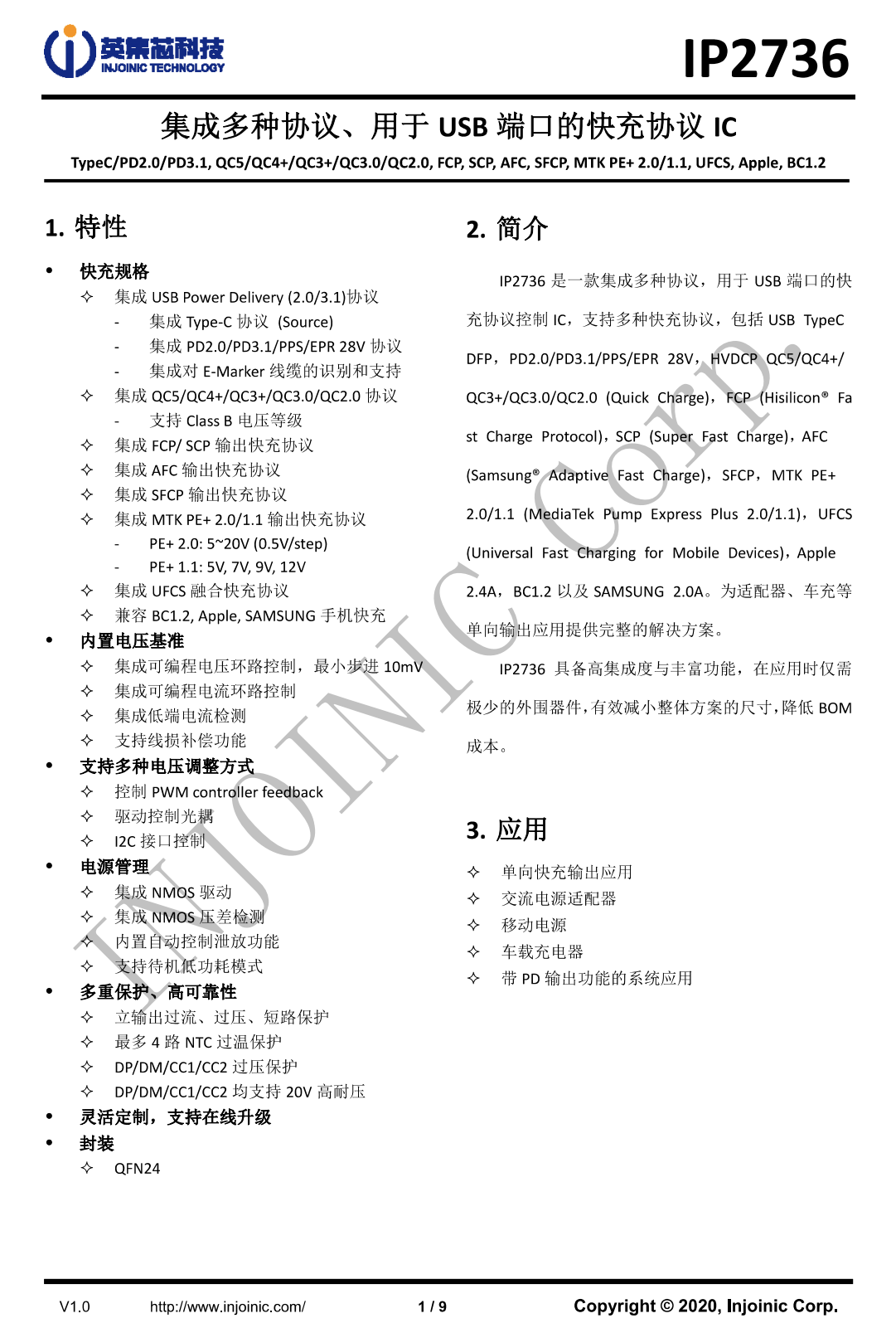
Here is the information about Injoinic IP2736.
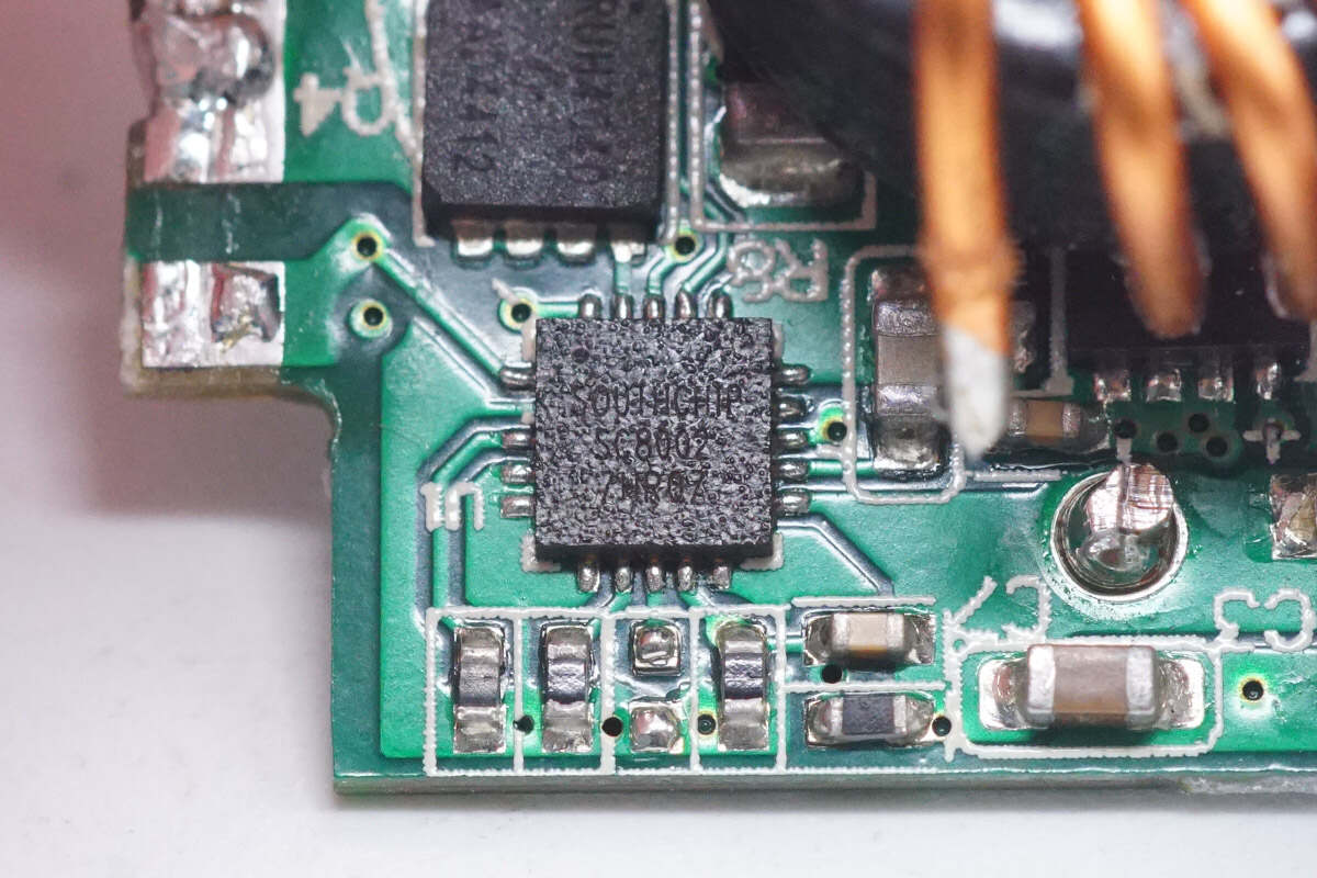
The synchronous buck controller is from SouthChip. It can be configured as dual output or single output. The total output voltage can be set by resistors for constant power control. Model is SC8002.
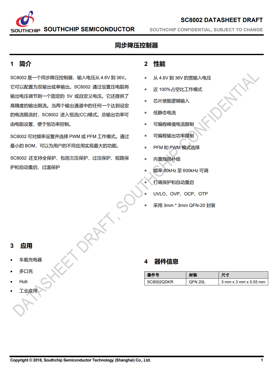
Here is the information about SouthChip SC8002.
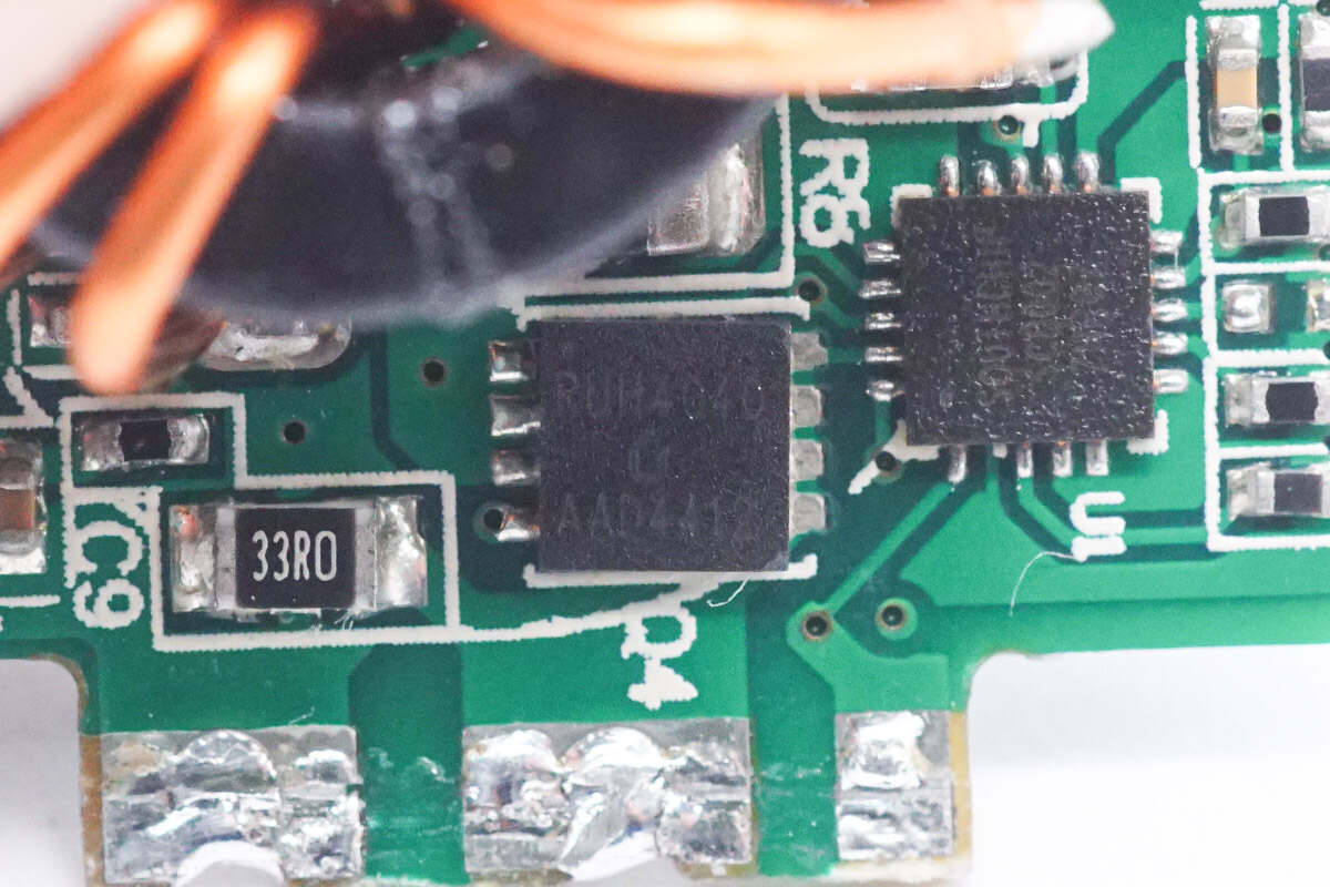
The synchronous buck MOSFET is from Ruichips and adopts PDFN3333 package. Model is RUH4040M2. 40V 5.5mΩ.
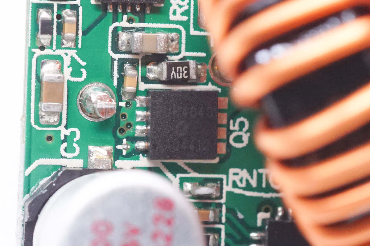
The synchronous buck MOSFET is the same as the previous one.
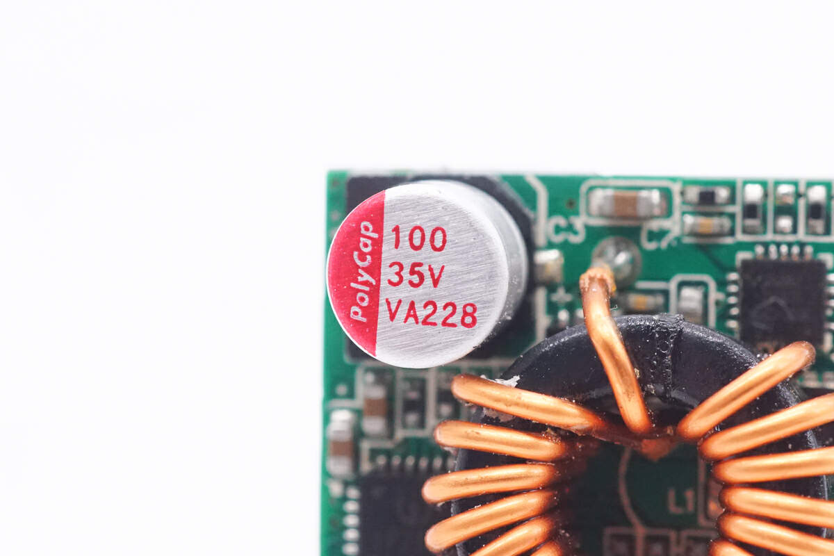
The SMD solid capacitor for output filtering is from PolyCap VA series. 100μF 35V.
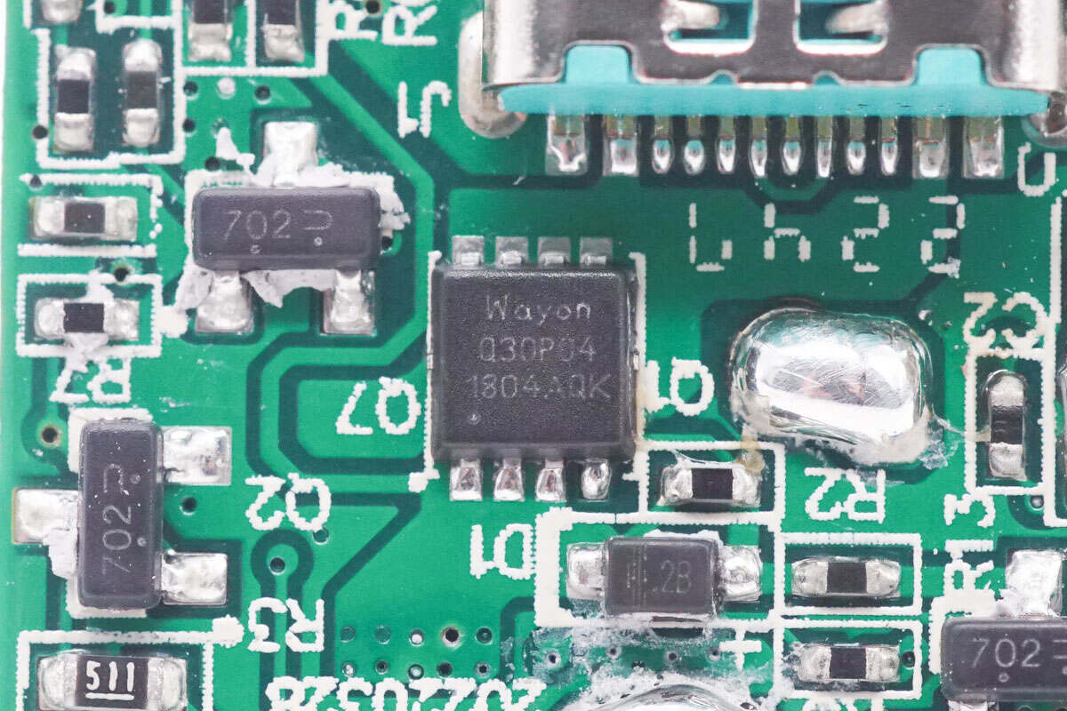
The VBUS MOSFET is from WAYON and adopts PDFN3030-8L package. Model is WMQ30P04T1. 40V 10mΩ.
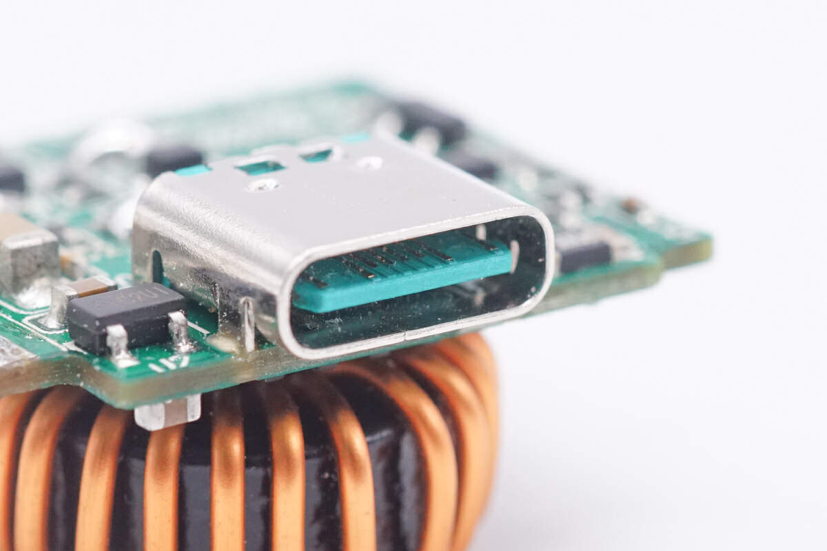
The USB-C socket has a green plastic sheet.
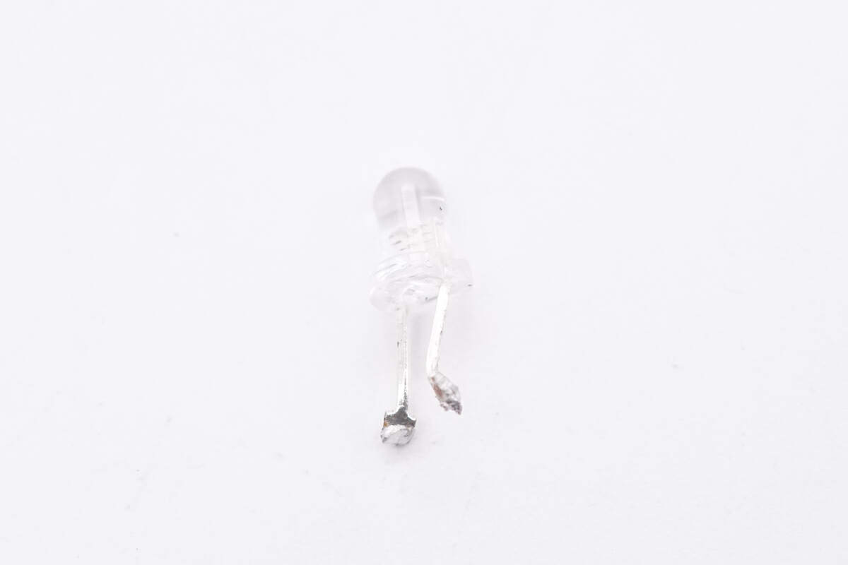
Here is the LED indicator.
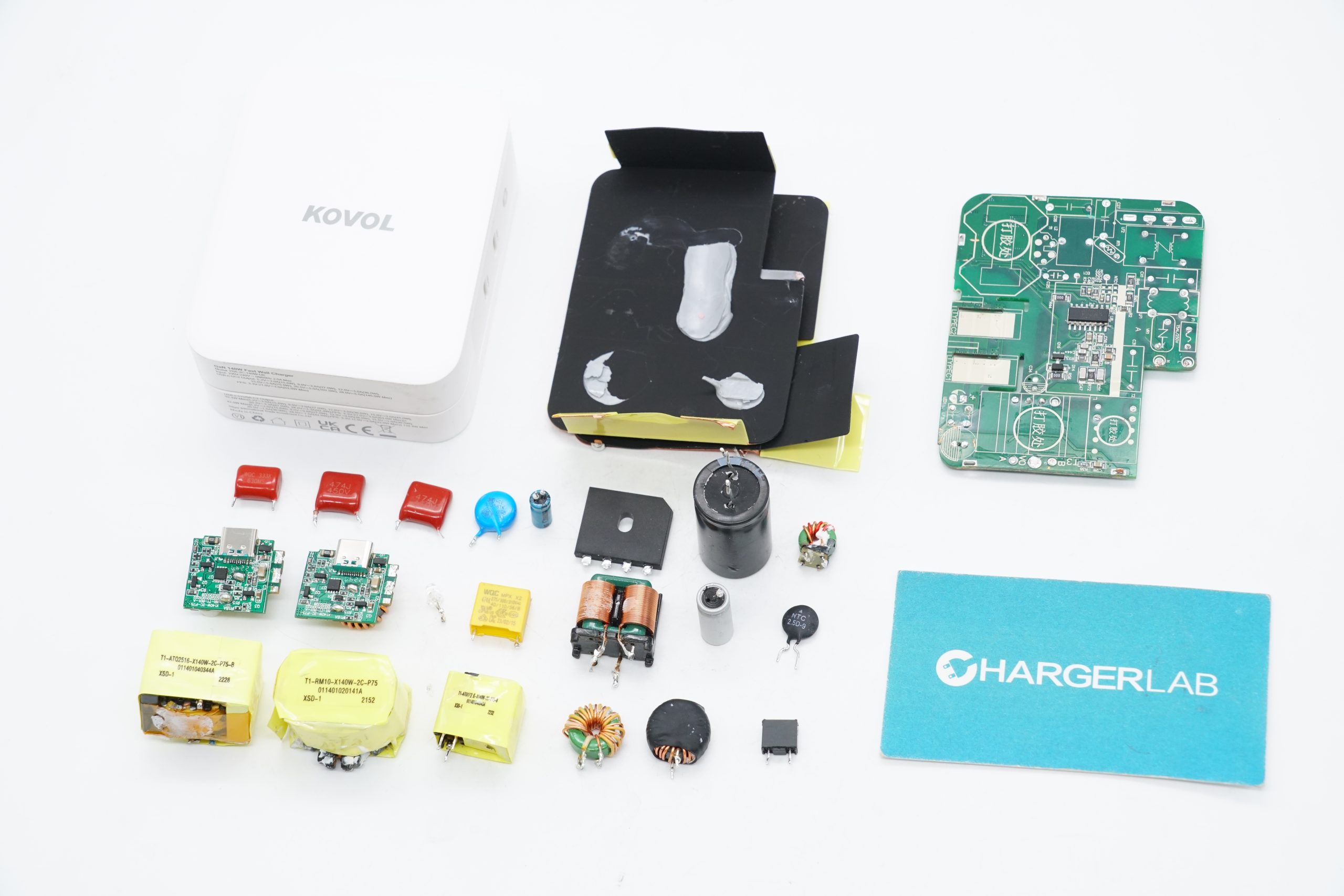
Well, those are all components of the Kovol 140W PD3.1 dual USB-C GaN charger.
Summary of ChargerLAB
The Kovol 140W PD3.1 dual USB-C GaN charger has a white matte surface. The foldable prongs it comes with make it easy to carry. It also has an indicator that will light up blue when powered on.
After taking it apart, we found it adopts a PFC circuit and LLC topology with fixed output voltage, and two independent buck circuits. It adopts a lot of thermal pads and copper sheets for heat dissipation. And the PCBA module is filled with pounding compound. All of which can keep the charger not too hot while charging. It can be the alternative to the Apple 140W charger, because of the similar two independent buck circuits, two USB-C ports, and a smaller size.
Related Articles:
1. Teardown of UGREEN 65W 3-in-1 Nexode RG GaN Charger (CD361)
2. Teardown of DeWalt 65W Charger of the Charging Kit (2AEK0655)
3. Teardown of LDNIO 140W GaN 6-in-1 Desktop Charger (A6140C)


