Introduction
HARMAN InfinityLab is a well-known digital accessories brand whose products include power banks, chargers, data cables, and speakers. The products are stylish, compact, and easy to carry and use. They adopt recycled plastic and are packaged in plastic-free packaging, which is more environmentally friendly.
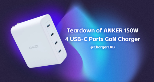
ChargerLAB has gotten a new InfinityLab ILINC 100W 2A2C GaN charger with a build-in GaN switch transistor from GaN Systems, which has a smaller size and better performance. Let's take it apart.
Unboxing

The front of the box is printed with the InfinityLab logo, product name, appearance and prong icons.

The package includes the charger, three replaceable prongs and a storage bag.

The three prongs are American standard, European standard and British standard.

Assemble the prongs with the charger body.

The center area of the prong side is yellow with the InfinityLAB logo.

The charger's front, back and side are gray, with a frosted surface.

The 100 is printed on the front, showing the maximum output power of the charger.

There are three icons on the other side.

The bottom is printed with the parameters.

The parameters are:
Model: ILINC100W
Input: 100-240V~50/60HZ 1.8A
USB-A1/A2 output: 5V3A 15W
USB-C1/C2 output: 5V3A, 9V3A, 12V3A, 15V3A, 20V5A
Total output: 100W Max
The charger has EAC, UKCA, TUV, CE and Level VI efficiency certification.

It has two USB-C ports, two USB-A ports and a LED indicator.


Its size is about 88.28 X 66.17 X 33.8 mm (3.47 X 2.6 X 1.33 inches).

Compared with the Apple 96W charger, it is slightly narrower and taller.

The weight of the charger and American standard prongs is about 254g (8.95oz).

The indicator light is light green.

The ChargerLAB POWER-Z KT002 finds that the USB-A port supports the Apple 2.4A protocol.

The other USB-A port also only supports the Apple 2.4A protocol.


The USB-C port only supports the PD3.0 fast charging protocol and five fixed PDOs of 5V3A / 9V3A / 12V3A / 15V3A / 20V5A.


The other USB-C port is the same as the previous one in protocol and PDO. Either USB-C1/C2 can support up to the maximum output separately.
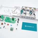
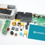
Teardown

Open the cover soldered by ultrasonic. The aluminum heat sink is covered with insulating mylar for heat dissipation of the PCBA module.

The transformer, electrolytic capacitor and other components are covered by adhesive to dissipate heat.

The plug is a separate module, soldered by the wire and insulated by the heat shrink tube.

The plug is connected to the PCBA module by the wire.

The edge of the PCBA module is wrapped with insulating tape.

The other side is the same.


The PCBA module's size is about 79.9 X 60.35 X 26.43 mm (3.14 X 2.37 X 1.04 inches).

The PCBA module consists of a small board and the main board. The small board is soldered with a receptacle and a secondary step-down circuit.

The plastic sheet is used to insulate between the step-down inductor and the primary components.

In the front of the PCBA module, the right is the secondary step-down circuit, the left is the filter capacitor, LLC resonant inductor and resonant capacitor, and the center is the PFC step-up inductor, and the bottom is the LLC transformer.

In the back of the PCBA module, two bridge rectifiers are on the top, two synchronous step-down converters are on the top left, and two synchronous rectifiers are on the bottom left. On the right side are the PFC step-up controller, step-up switch transistor, rectifier, LLC controller and switch transistor. The low voltage and high voltage components are insulated by Myla.
The 100W charger adopts PFC + LLC. Two USB-C ports use separate step-down circuitry controlled by the protocol chip. The two USB-A ports use a step-down circuit with a fixed 5V output.
Now let's have a look at the input side.

There are the fuse, varistor, common mode choke, X2 safety capacitor and other components on the input side.

The time-delay fuse is 5A 250V.

The blue 10D511K varistor from Songtian Electronics is for overvoltage protection.

The common mode choke adopts the insulating wire wound on a green magnetic ring.

The 0.33μF X2 safety capacitor is from WQC.

The secondary common mode choke is wound with flat copper wire and fixed with adhesive in the middle.

Two bridge rectifiers are from PY TBMR610, using the parallel half-bridge to connect and reduce temperature rise.

The rectifier output supplies power to the PFC circuit through a filter circuit consisting of two 0.47μF 450V film capacitors and a magnetic ring inductor.

The filter inductor is wrapped with copper tape and fixed by a heat shrink tube.

The PFC controller is the NXP Semiconductors TEA19162 for the step-up rectified voltage. It integrates X capacitors without external components, supporting high-precision boost and multiple protections.

The PFC switch transistor is from GaN Systems GS-065-011-1-L, printed with GS6511-1L. It is a GaN FET with a resistor of 150mΩ, withstand voltage of 650V and a package of PDFN5*6.

Here are the details of the GaN Systems GS-065-011-1-L.

The PFC rectifier is from PW ES5JGR, which is a 5A diode.

The 150mΩ sampling resistor with a 2512 package is used to detect the PFC current, whose top side is a 500mΩ resistor in the 1206 package.

The PFC step-up inductor and LLC transformer are soldered on the same small board with L2 and T1 marked on the top, respectively.

The high voltage filter capacitor, LLC resonant inductor and resonant capacitor are soldered on the side of the main PCB board.

The two high-voltage capacitors for PFC output filtering are from JSH, with the specification of 420V 39μF.

The LLC controller TEA19161T and TEA19162, a half-bridge resonant switching power supply with PFC, is used to improve power conversion efficiency.

Two LLC switch transistors from SemiHow HCFL65R210 are the NMOS with withstand voltage of 650V, a resistor of 200mΩ and a package of DFN8*8.

The LLC resonant capacitor has a specification of 0.022μF and a withstand voltage of 630V.

The resonant inductor is labeled on the top.

Diodes are soldered on the back of the transformer board for rectification.

The 35V 47μF filter capacitor is used to power the two controllers, TEA19162 and TEA19161T.

The small and light SMD Y capacitor TMY1102M comes from TRX, which is well suited for high-density power supply products such as GaN fast chargers.

This is the 1009 optocoupler for voltage feedback.

The two synchronous rectifiers are from Hunteck HGN098N10AL, the NMOS with the withstand voltage of 100V, resistor of 8mΩ and package of DFN5*6.

Remove the components from the main PCB board. The synchronous rectifier controller, solid filter capacitor, inductor, step-down inductor and filter capacitors are on the secondary side.

The secondary synchronous rectifier controller is from the NXP Semiconductors TEA1995T, which has two built-in drivers for synchronous rectification of the LLC switching power supply. It supports 4.5-38V output voltage and is suitable for multiple modes of synchronous rectification with simple components outside.

The two solid filter capacitors are from JSH, with the specification of 820μF 25V.

The four MLCCs in the 1206 package and solid capacitors are in parallel.

This is the output filter inductor.

A 220μF 25V filter capacitor follows the filter inductor.

Two protocol chips, buck switch transistor and filter capacitor are also soldered on the small board where the USB-A and USB-C receptacles are soldered. The upper right corner is the thermistor for detecting the transformer's temperature and shutting down the output for overheating protection. On the right side are two LED indicators.

A step-down inductor is soldered on the back of the small board for the 5V output of the two USB-A ports.

The USB PD IC uses the Weltrend WT6636F, a protocol chip (TID number: 1080018) that has passed the USB-IF USB PD3.0 (PPS) certification (TID number: 1080018), in addition to Qualcomm QC4+ certification, with the certification number of QC20200316138. It supports USB PD3.0 and PPS, has built-in programmable control, and integrates a current sampling amplifier.

Both USB-C port protocol chips are from Weltrend WT6636F, supporting intelligent power distribution. Either USB-C1/C2 can support up to 100W output separately.

The USB-C port uses the Toll Microelectronic TMI2286D synchronous step-down converter, which withstands the voltage of 30V in the SOP8 package.

The other USB-C port also uses the Toll Microelectronic TMI2286D synchronous step-down converter.

A PMOS with the withstand voltage of 30V, resistor of 20mΩ and package of DFN3*3, the Hunteck HTM200P03 MOSFET outside the TMI2286D is to reduce the output pressure drop.

This is the other step-down inductor.

The output solid filter capacitor has a specification of 220μF 25V.

The other two filter capacitors used for input and output both have a specification of 220μF 25V.

The VBUS switch transistor from ARK AKF30N5P0S, printed with 30N5P0S, is an NMOS with a withstand voltage of 30V, resistor of 4.2mΩ and package of PDFN3333.

The other VBUS switch transistor is the same.

The step-down controller for two USB-A ports is from Southchip SC8002, which supports 36V input, high-precision output and separate current limiting for two channels. The SC8002 can be used for car chargers, multi-port chargers, USB HUB, etc.

Here are the details of the Southchip SC8002.

The input filter capacitor's specification is 150μF 25V.

Two Huayi Microelectronics HY1503C1 synchronous step-down switch transistors soldered between the two USB-A ports are the NMOS with the withstand voltage of 30V, resistor of 7.1mΩ and package of DFN3*3.

The step-down inductor is fixed with adhesive and wound by two wires, with an insulating board at the bottom to insulate the PCB.

The two USB-A ports adopt the SMEI CW3005F chip and support the Apple 2.4A protocol.

There are the sampling resistor and the LM321 operational amplifier for output power distribution control.

There are the other sampling resistor and the LM321 operational amplifier for output current detection.

The filter capacitor for USB-A port output has a specification of 150μF 6.3V.

The other USB-A port has the same filter capacitor.

The thermistor is covered with a heat shrink tube and insulated with high-temperature tape.

This is the USB-C1 receptacle with the black core, soldered and fixed by the vertical via.

The USB-C2 receptacle is the same.

The USB-A receptacle is insulated by wrapping high-temperature tape.

The other USB-A receptacle is the same.

OK, that's all for the teardown of the InfinityLab ILINC 100W 2A2C GaN charger.
Summary of ChargerLAB
HARMAN InfinityLab is a well-known digital accessories brand whose products include power banks, chargers, data cables, and speakers. The products are stylish, compact, and easy to carry and use. They adopt recycled plastic and are packaged in plastic-free packaging, which is more environmentally friendly.
The new InfinityLab ILINC 100W 2A2C GaN charger with a build-in GaN switch transistor from GaN Systems has a smaller size and better performance. It has three replacable prongs, the American standard, European standard and British standard.
It adopts PFC + LLC, 10D511K varistor from Songtian Electronics, safety capacitor from WQC, bridge rectifiers from PY TBMR610, NXP Semiconductors TEA19162 PFC controller, and so on. The components are qualified and reliable.
Related Articles:
1. Review of Asus Adol 100W GaN Charger
2. Review of UGREEN Nexode 3-in-1 65W GaN Charger
3. Teardown of Anker 100W USB-C Charger, 736 Charger (Nano II 100W)