Introduction
ChargerLAB got a 96W USB-C GaN from HP, model ADP-96AW A. It has a foldable plug and supports an input voltage of 100-240Vac. It has a USB-C output port and supports 20V4.8A 96W PD fast charging. Next, let's take it apart to see its internal components and structure.
Product Appearance
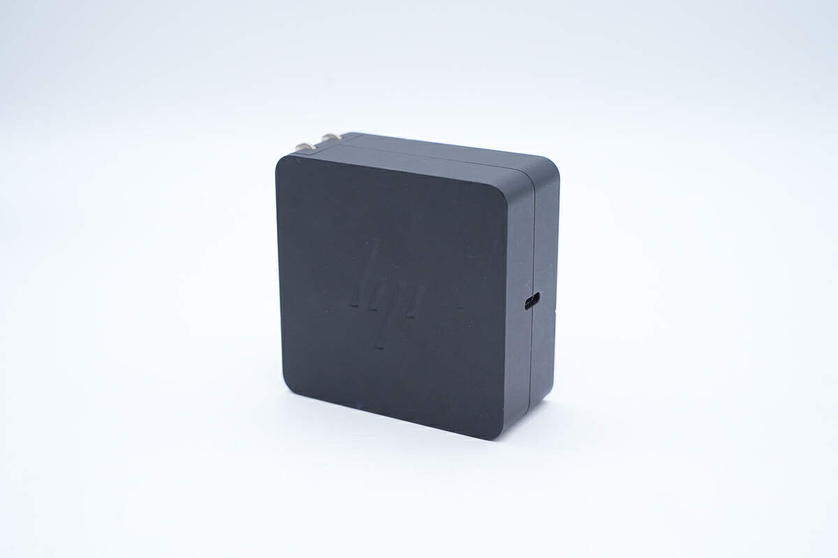
HP 96W USB-C GaN Charger adopts a black shell made of a fire-retardant PC, and the surface is frosted to resist fingerprints.
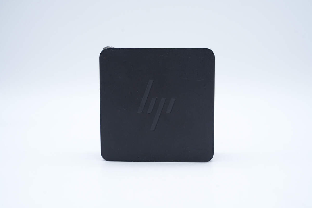
There is an HP logo in the center of the front.
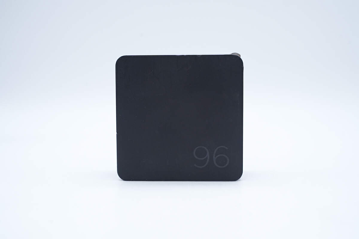
The word 96 is written on the lower right corner of the back, indicating the maximum output power of the charger.
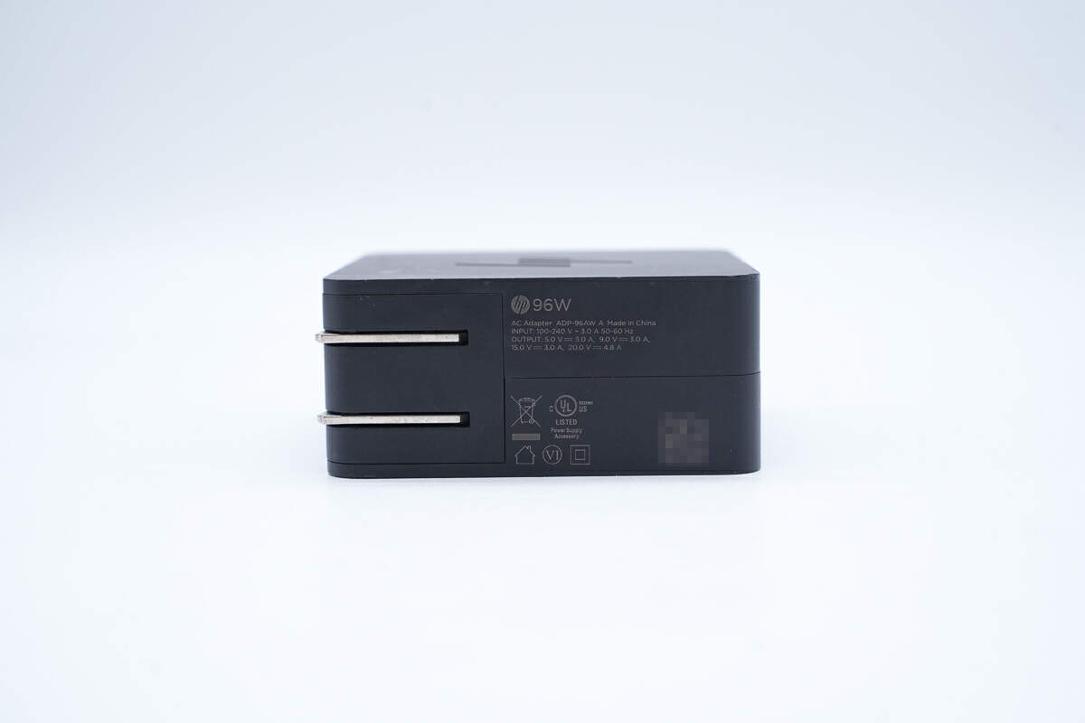
The specs info is printed at the bottom.
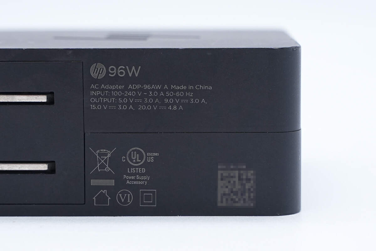
Model is ADP-96AW A. It can support an input of 100-240V~50/60Hz 3A. It can support outputs of 5V3A, 9V3A, 15V3A, and 20V4.8A. The maximum output is 96W. It is UL-certified and has Level VI energy efficiency certification.
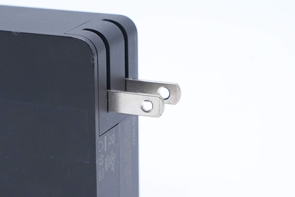
Here is the foldable plug.
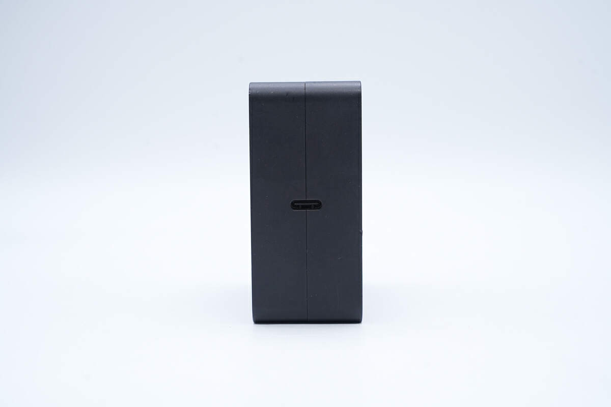
It only has one USB-C port.
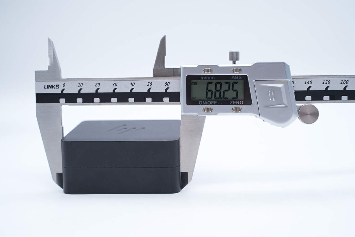
The length is about 68.3 mm (2.69 inches).
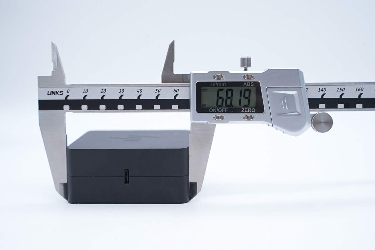
The width is about 68.2 mm (2.69 inches).
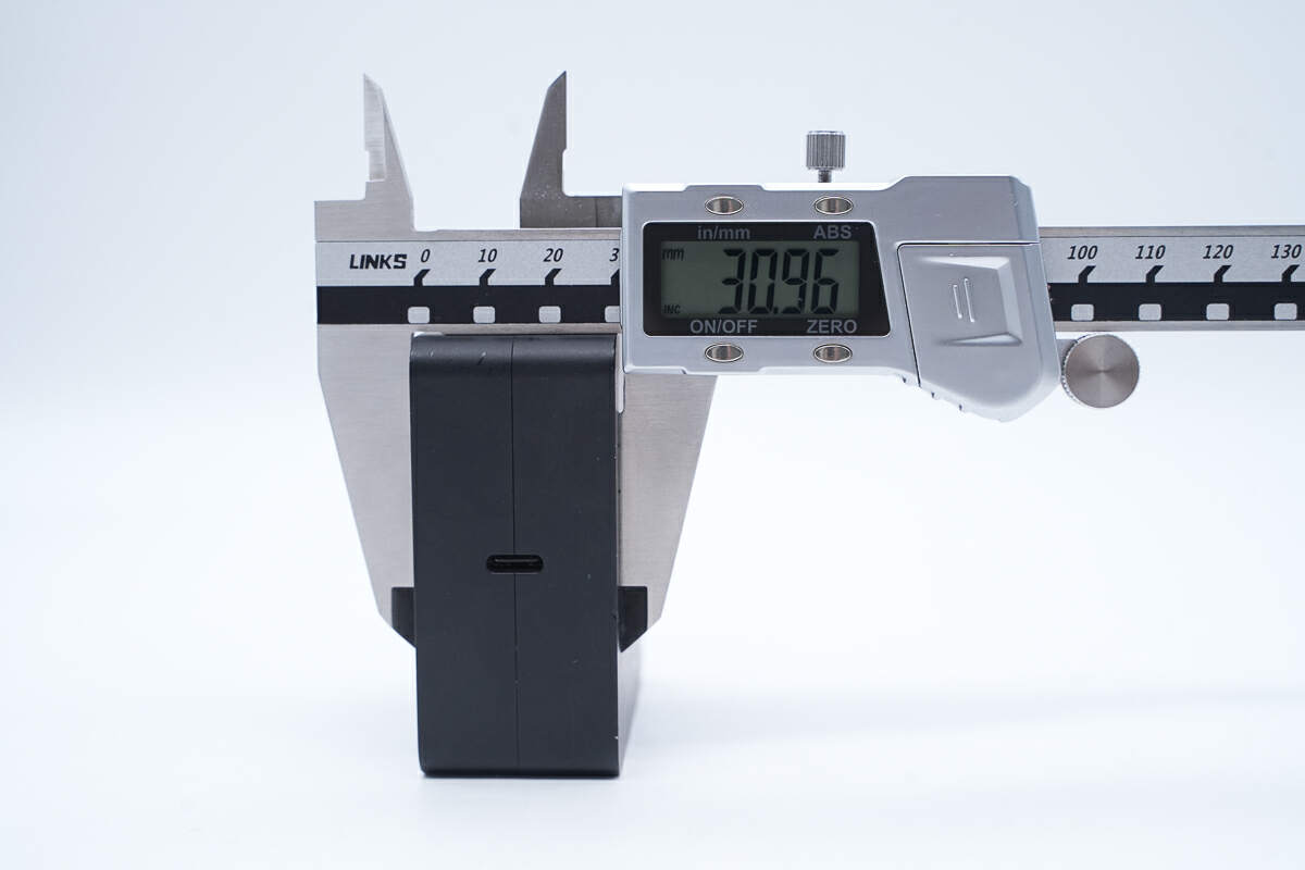
The thickness is about 31 mm (1.22 inches).
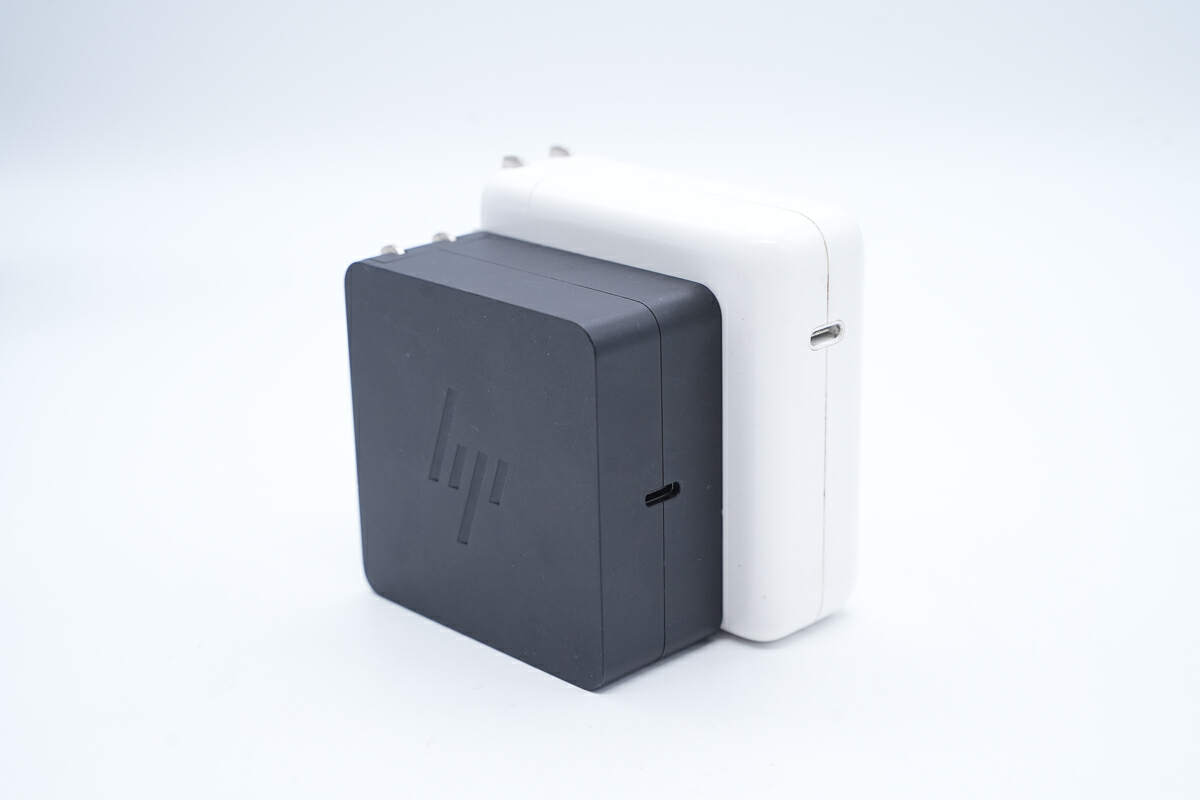
It is slightly smaller than the Apple 96W charger.
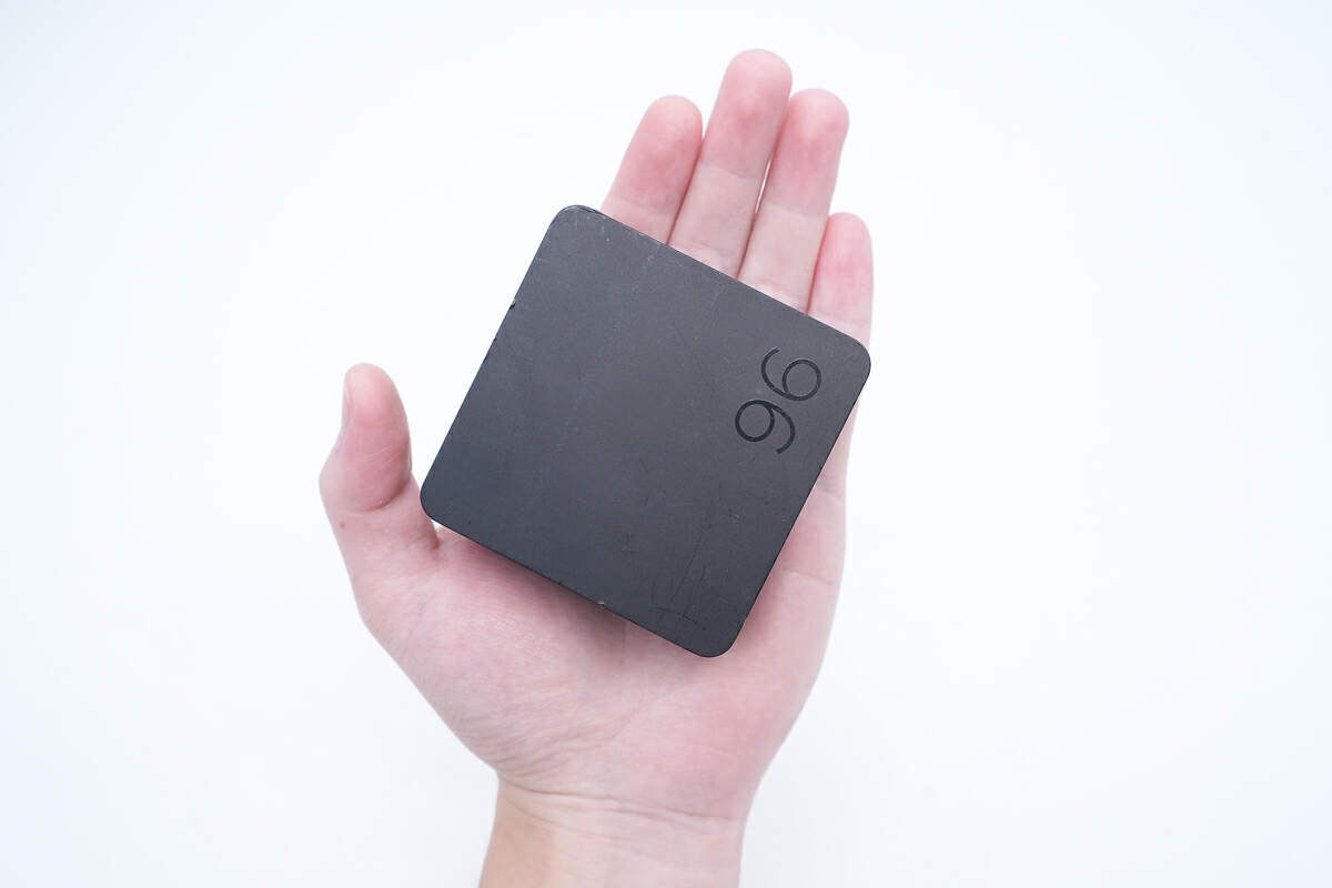
That's how big it is in the hand.
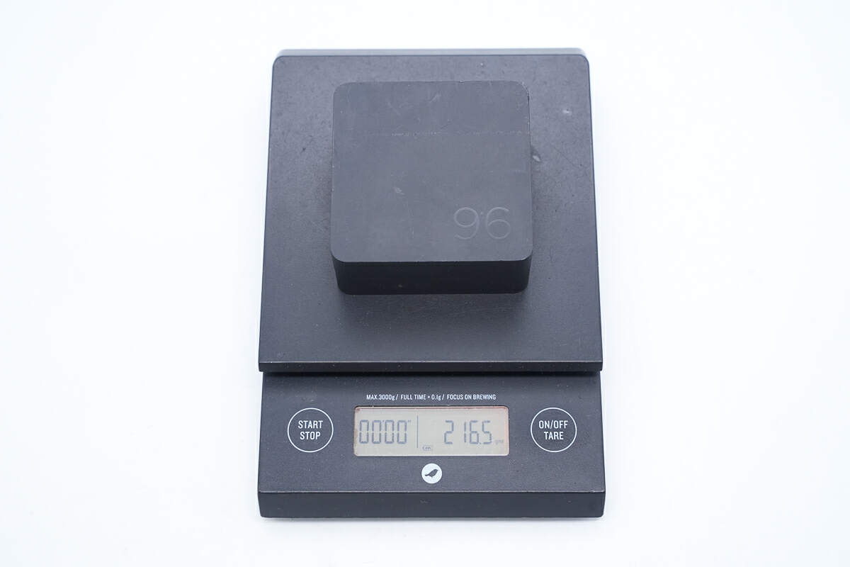
The weight is about 216.5 g (7.64 oz).
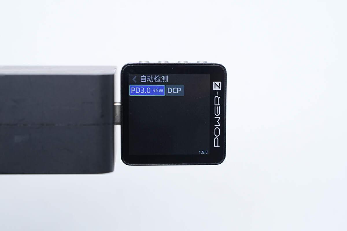
ChargerLAB POWER-Z KM003C shows the USB-C port can support PD3.0 and DCP charging protocols.

And it has four fixed PDOs of 5V3A, 9V3A, 15V3A, and 20V4.8A.
Teardown
Next, let's take it apart to see its internal components and structure.
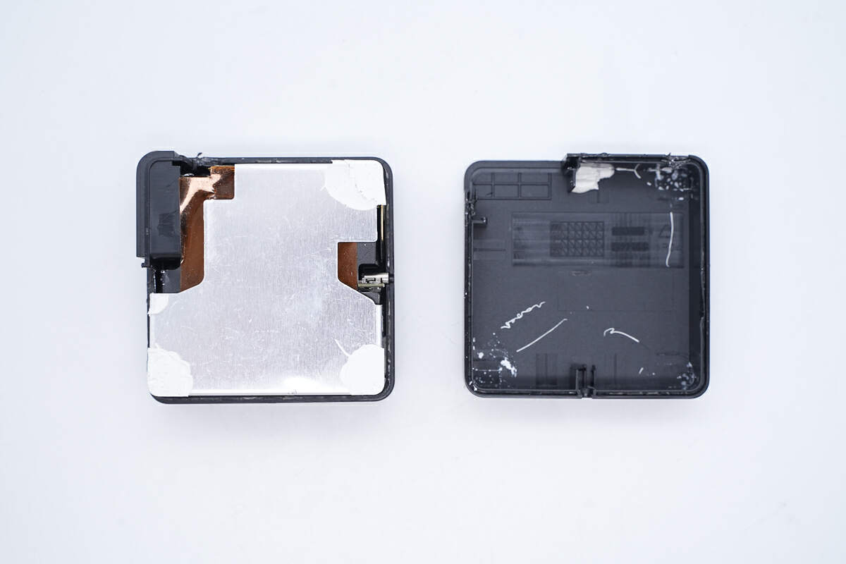
Pry open the shell.
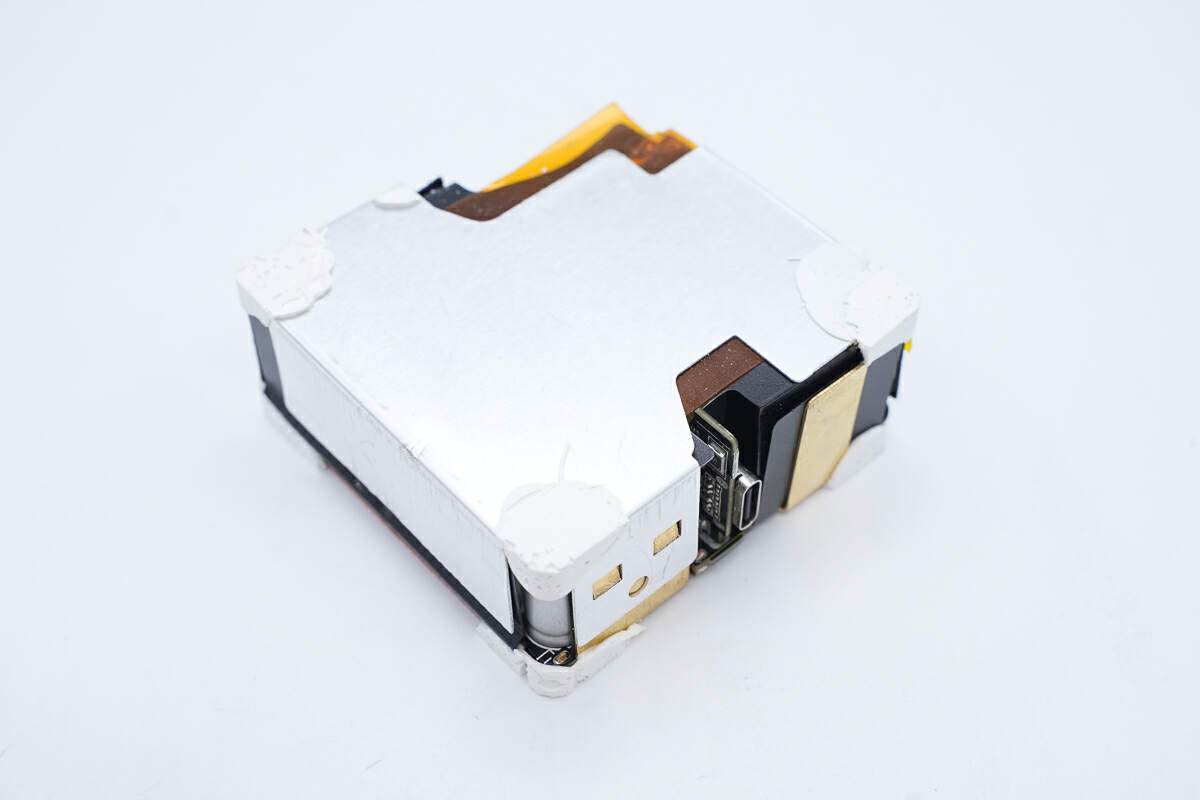
The top and sides of the PCBA module are covered with an integrated aluminum alloy heat sink, with glue at the three corners.
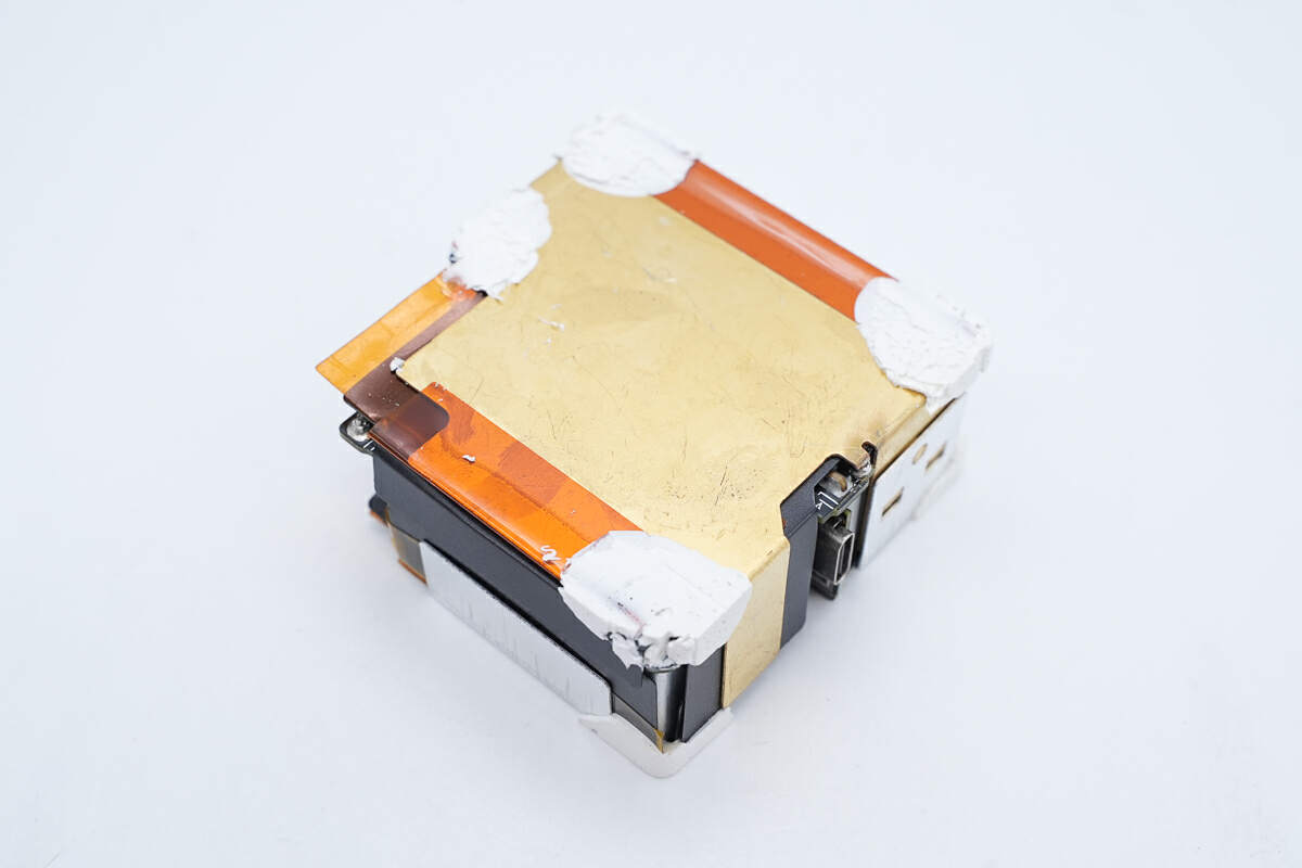
The bottom of the PCBA module is covered with a brass heat sink, and the corners are also glued.
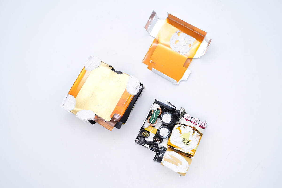
Remove the heat sink, and there is insulating tape on the inside of both pieces.
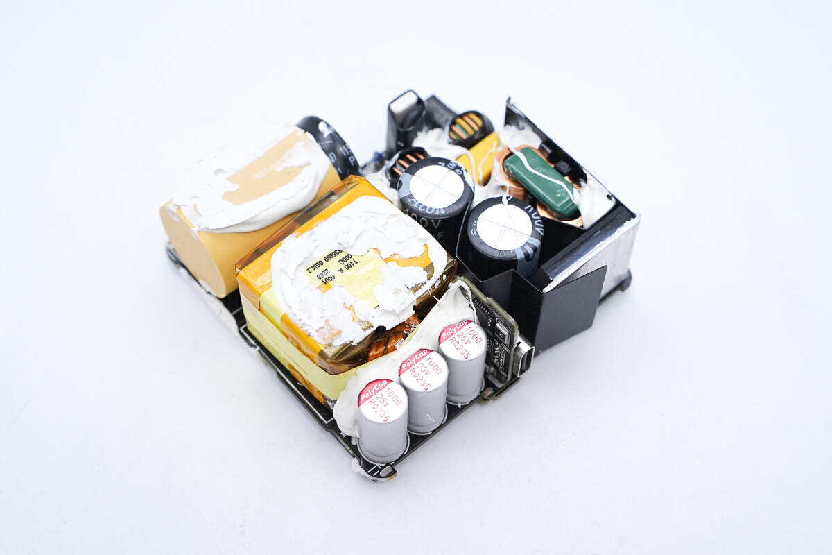
The components on the front of the PCBA module are reinforced by potting compound, and Mylar sheets are used to isolate the capacitors from the output PCB.
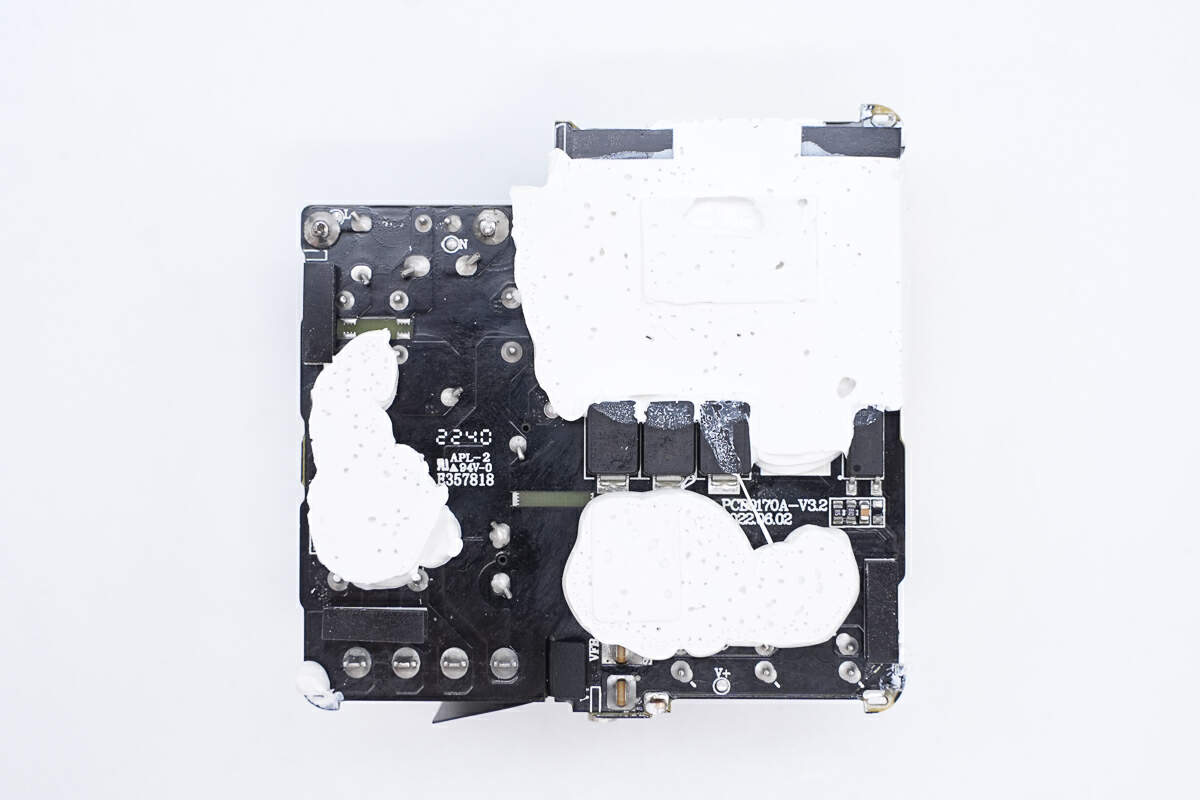
The potting compound on the back of the PCBA helps dissipate heat.
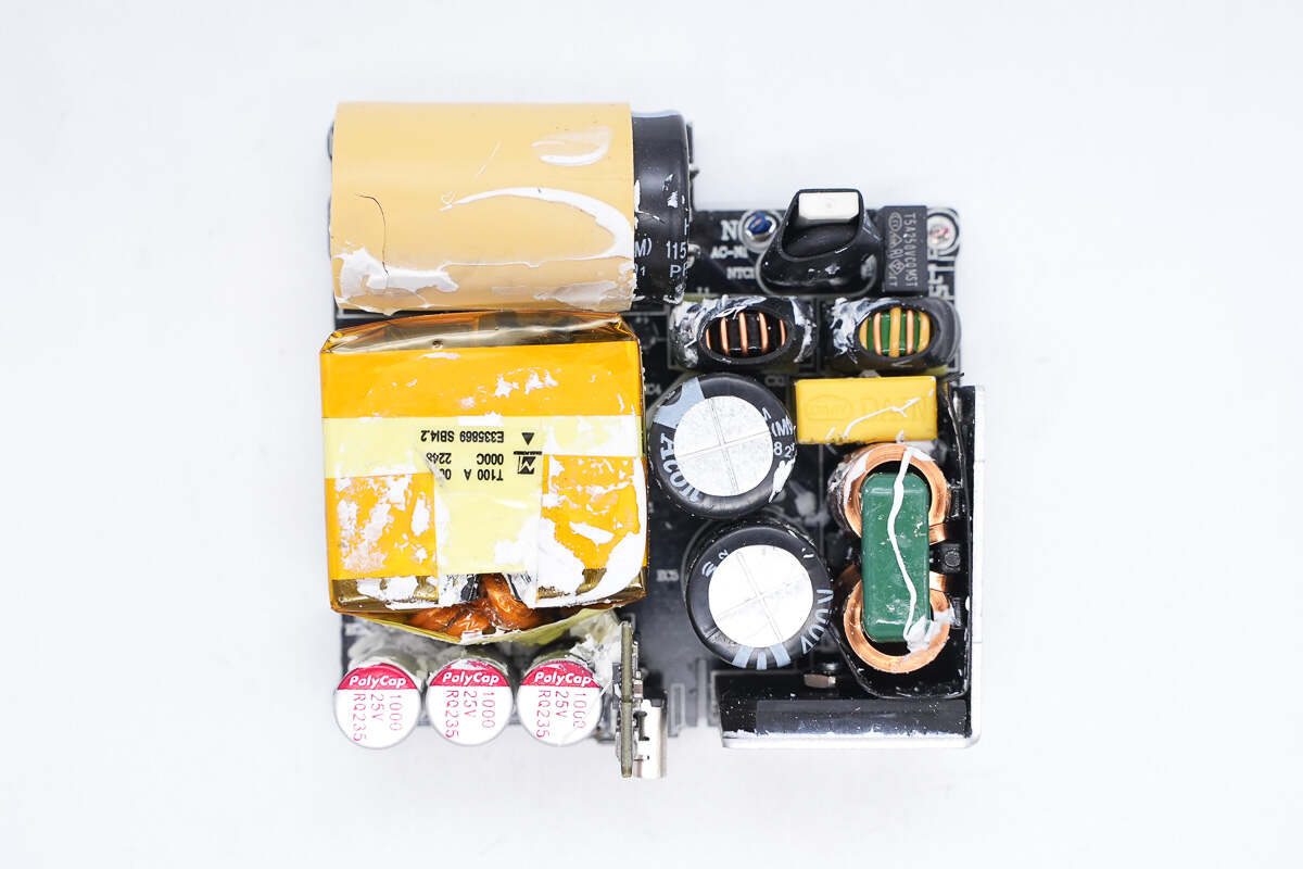
Clean up the potting compound. The components on the front of the PCB are arranged compactly and orderly, and heat sinks are provided on the edge to help the bridge rectifier dissipate heat.
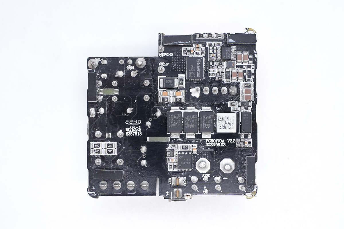
On the back of the PCB, there are the master control chip, Primary MOSFET, optocoupler, SMD Y capacitor, synchronous rectifier controller, and synchronous rectifier.
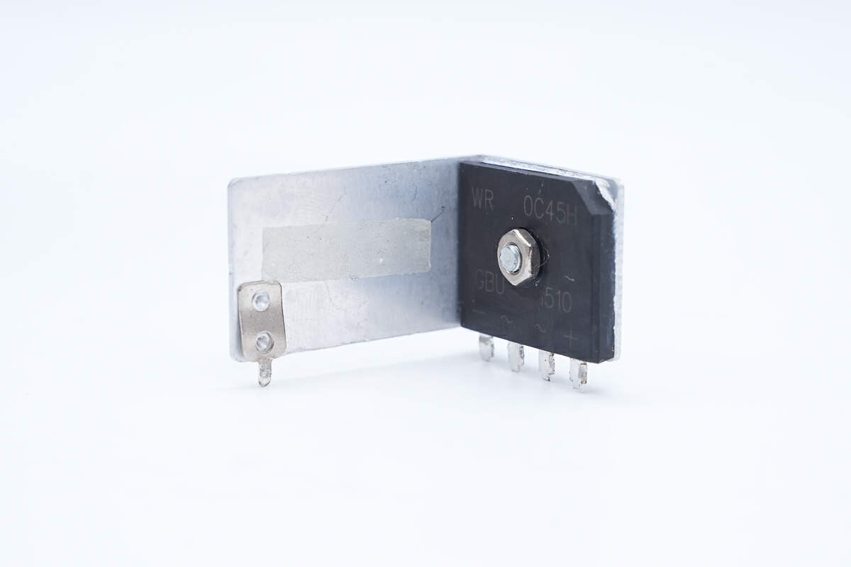
After removing the heat sink, the bridge rectifier is fixed on the heat sink with a screw.
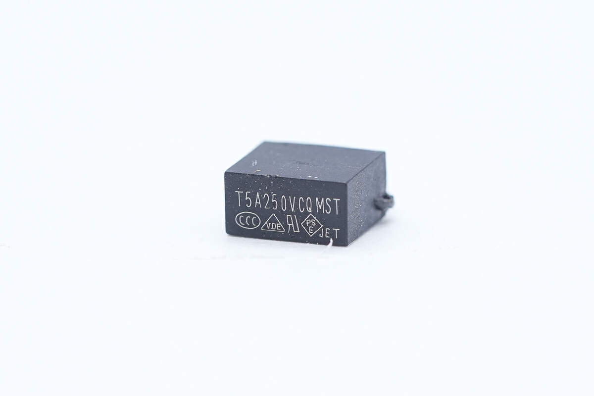
There is the time-delay fuse. 5A 250V
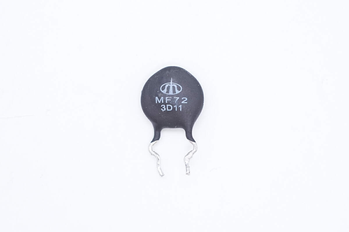
The NTC thermistor is used to suppress power-up surge current.
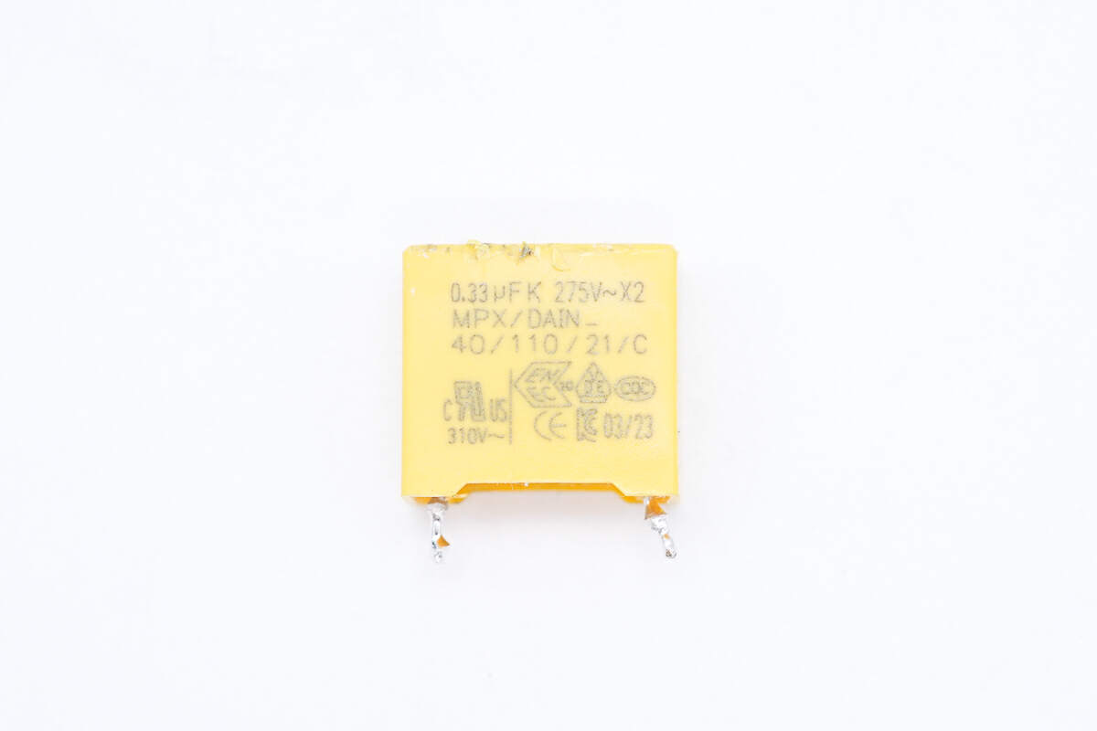
Here is the safety X2 capacitor. 0.33μF.
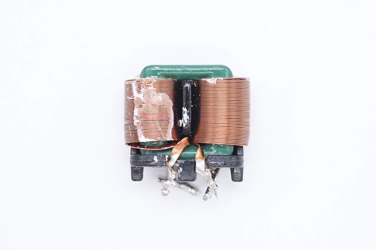
The secondary common mode choke is wound with flat copper wire and has a green core.
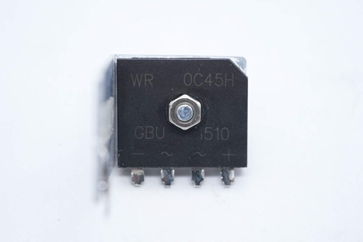
The bridge rectifier is from WORLD and adopts GBU package. The operating temperature is -55~+175℃. 15A 1000V. Model is WRGBU1510.
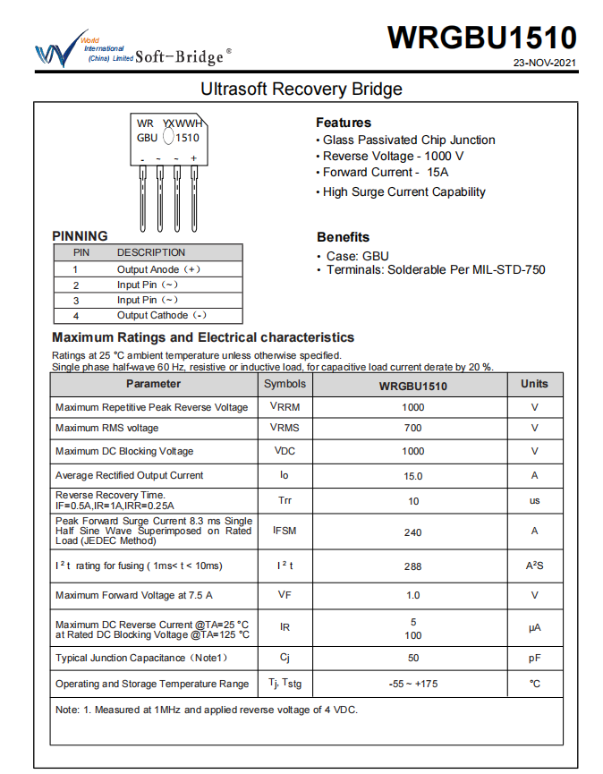
Here is the information about WORLD WRGBU1510.
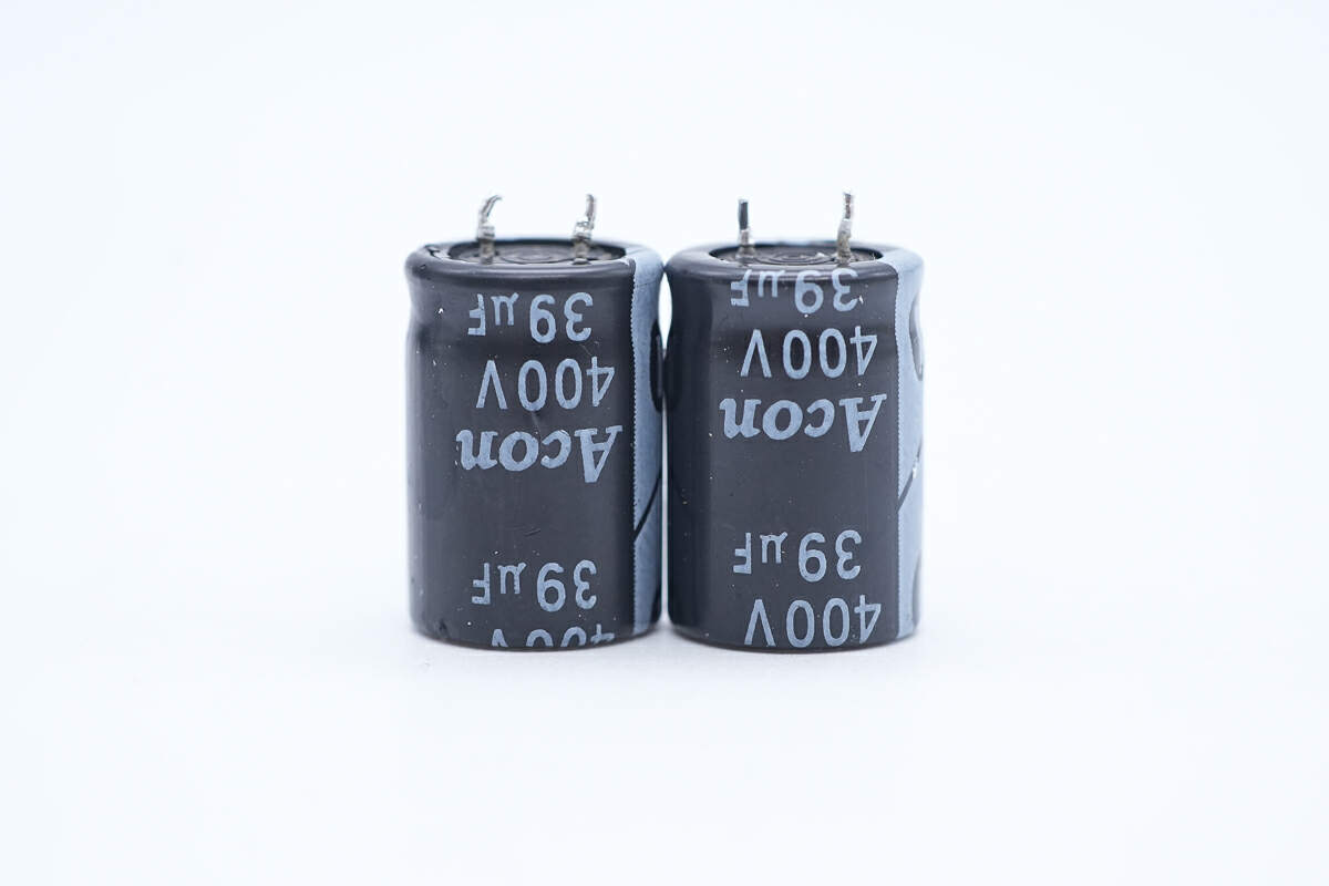
These two electrolytic capacitors are from Acon. 400V 39μF.
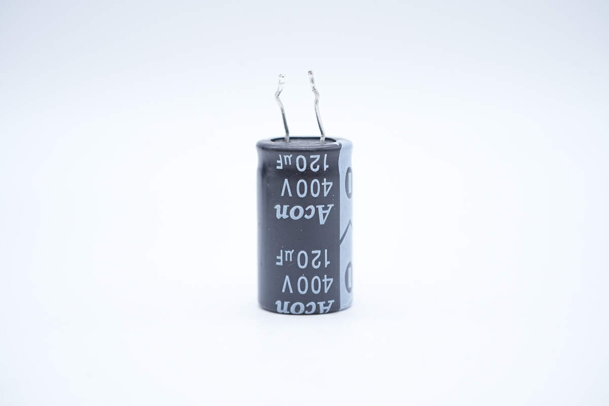
The third electrolytic capacitor is also from Acon. 400V 120μF.
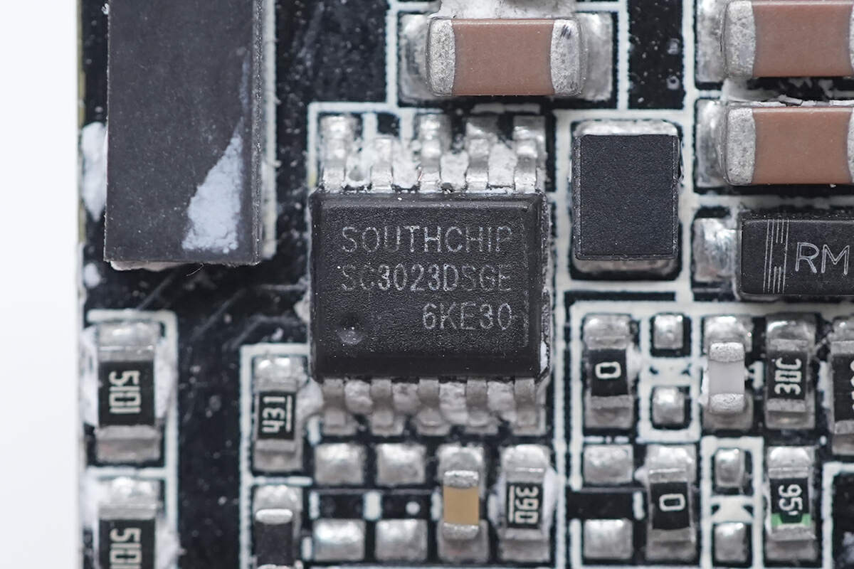
The master control chip is from SOUTHCHIP. It is a high-frequency quasi-resonant flyback controller with a built-in GaN driver that can be used to directly drive enhanced GaN FETs. The chip has built-in X-capacitor discharge and high-voltage startup and has an adaptive switching frequency foldback function. Model is SC3023.
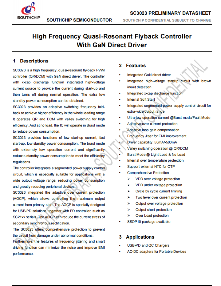
Here is the information about SOUTHCHIP SC3023.
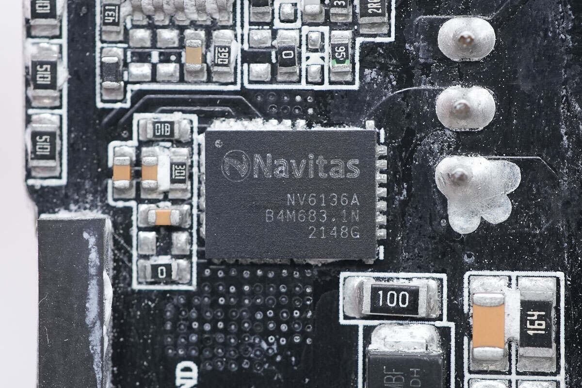
The primary MOSFET is from Navitas and adopts 6*8mm QFN package. This is a highly integrated GaN power chip. 170mΩ 700V. Model is NV6136A.
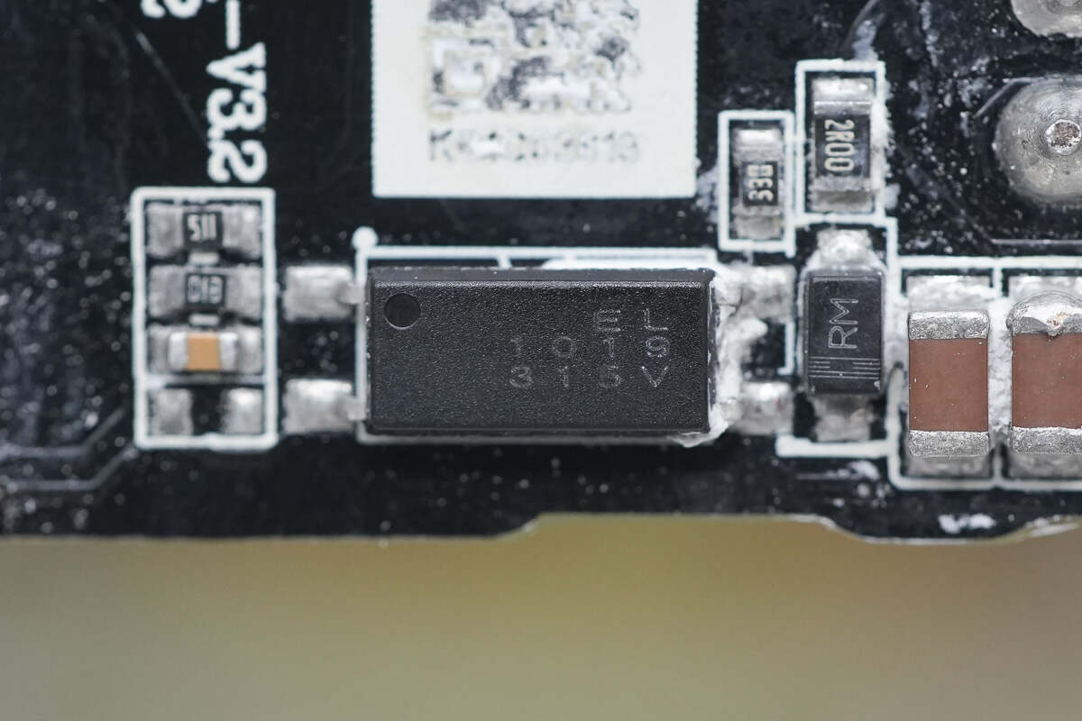
The optocoupler is from Everlight for output voltage feedback.
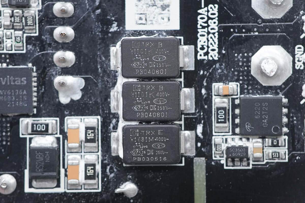
The SMD Y capacitor is from TRX. The part numbers are TMY1101K and TMY1681M, respectively.
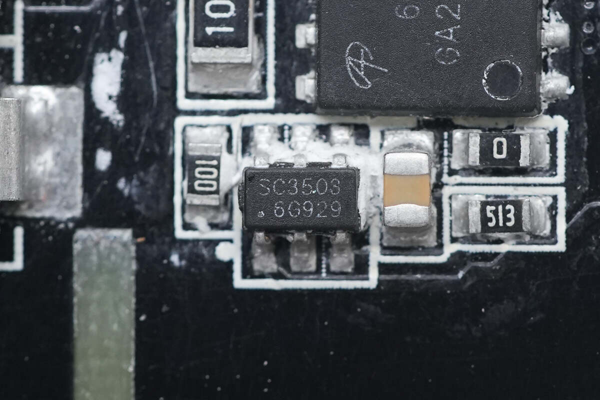
The synchronous rectifier controller is from SOUTHCHIP. It is an adaptive turn-on detection and fast turn-off synchronous rectifier controller, compatible with multiple MOS, and supports multiple working modes. Model is SC3503.
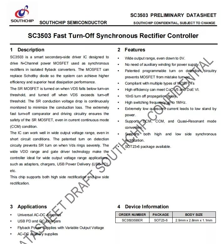
Here is the information about SOUTHCHIP SC3503.
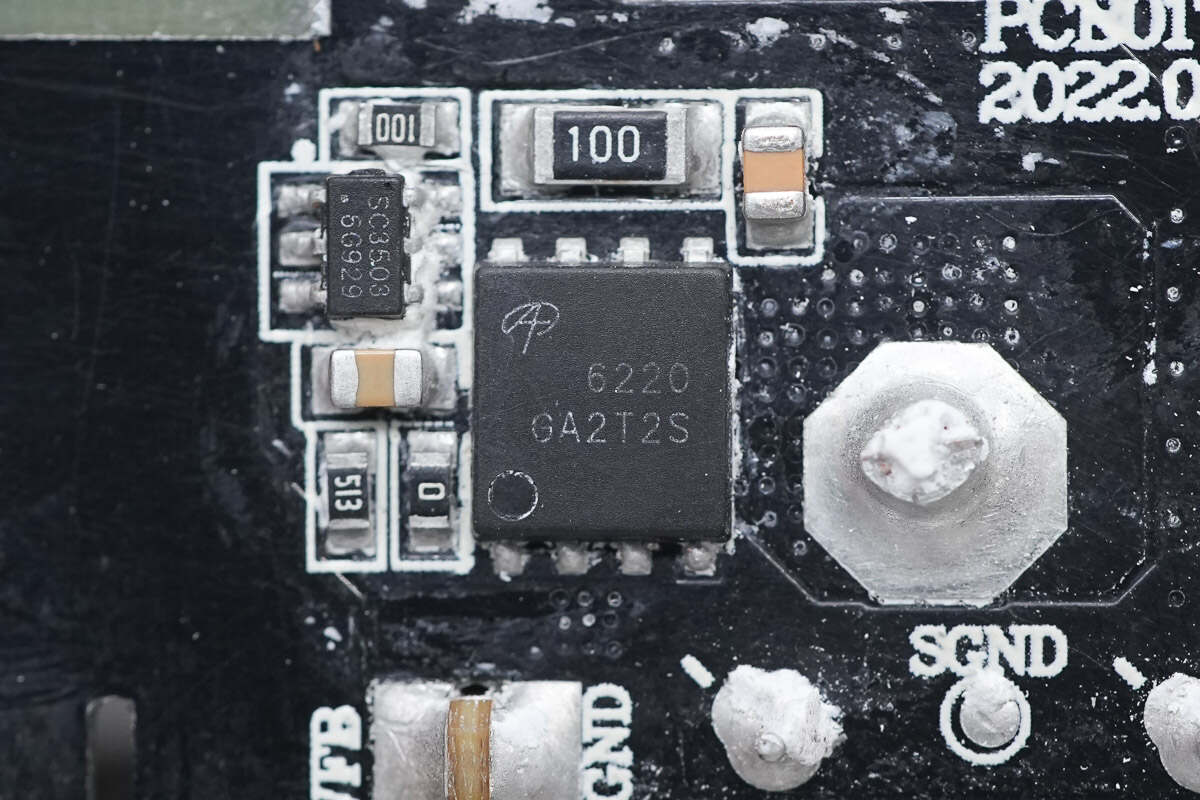
The synchronous rectifier is from AOS and adopts DFN5*6 package. 100V 5.1mΩ. Model is AON6220.
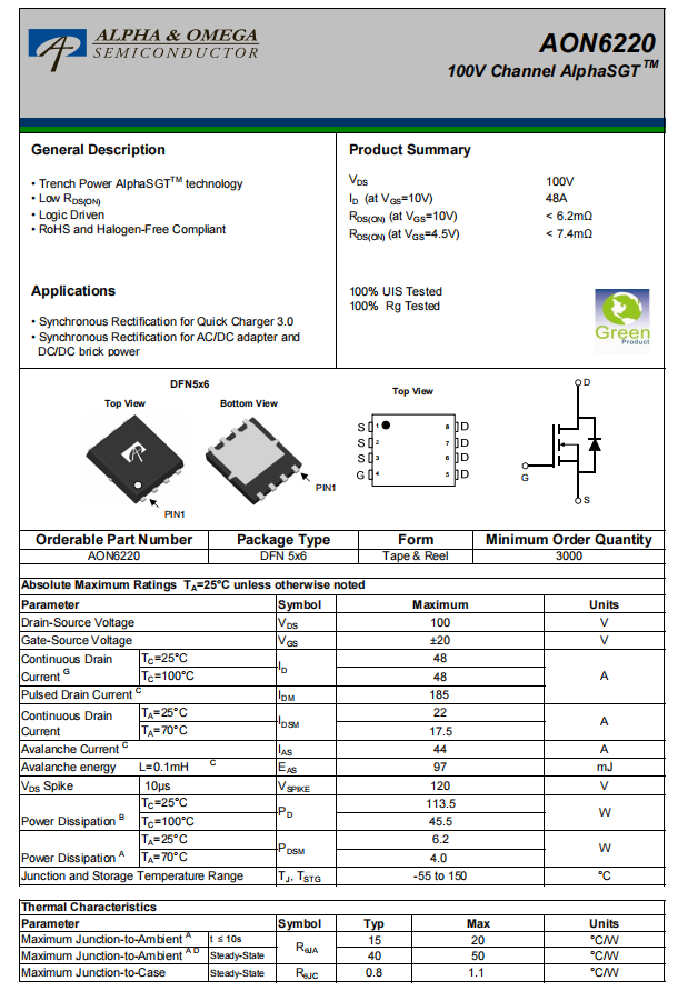
Here is the information about AOS AON6220.
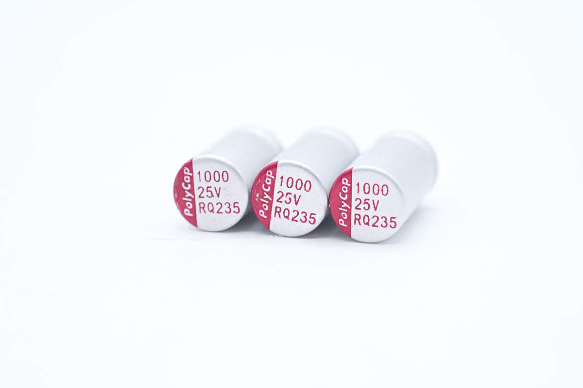
The three solid capacitors for output filtering come from PolyCap. 25V 1000μF.
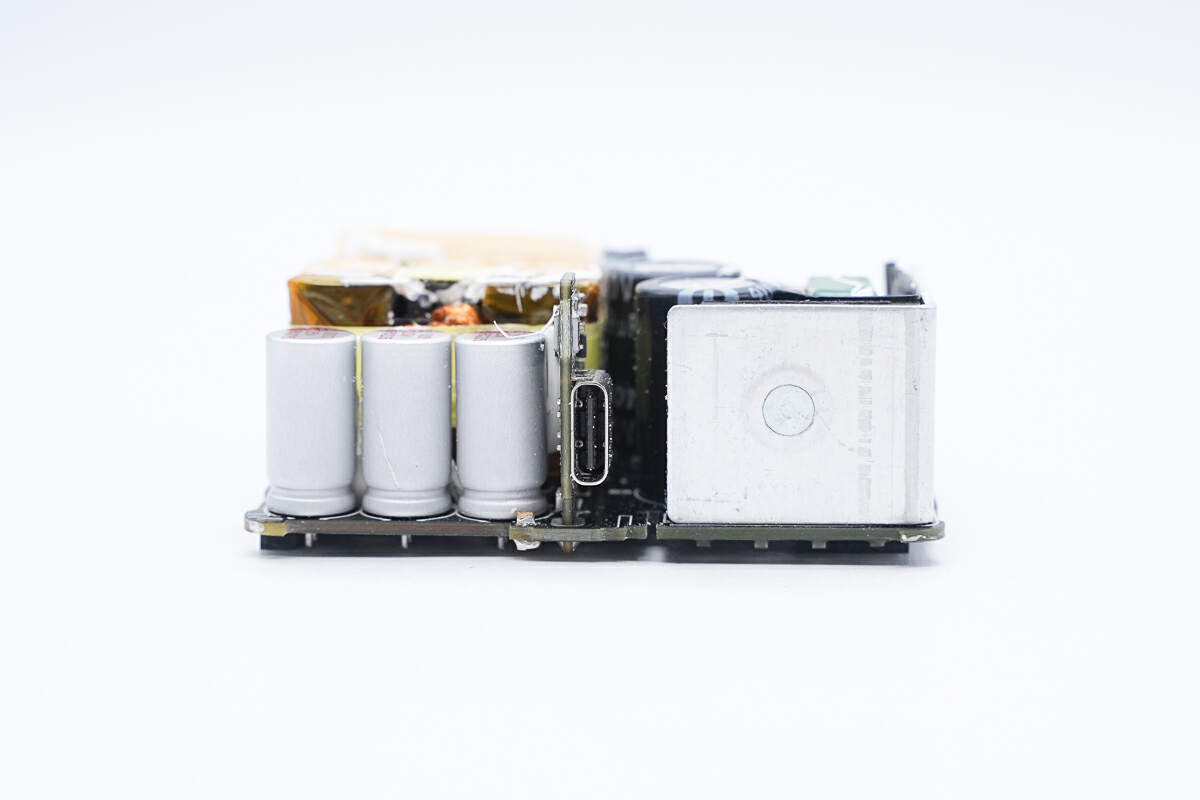
The USB-C socket is soldered on a small vertical PCB board.
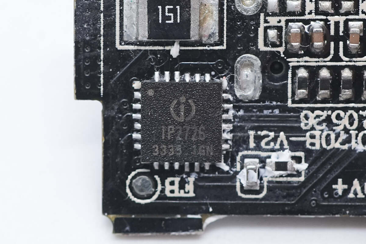
The protocol chip is from INJOINIC. It integrates multiple protocols for fast charging of USB output ports. Model is IP2726.
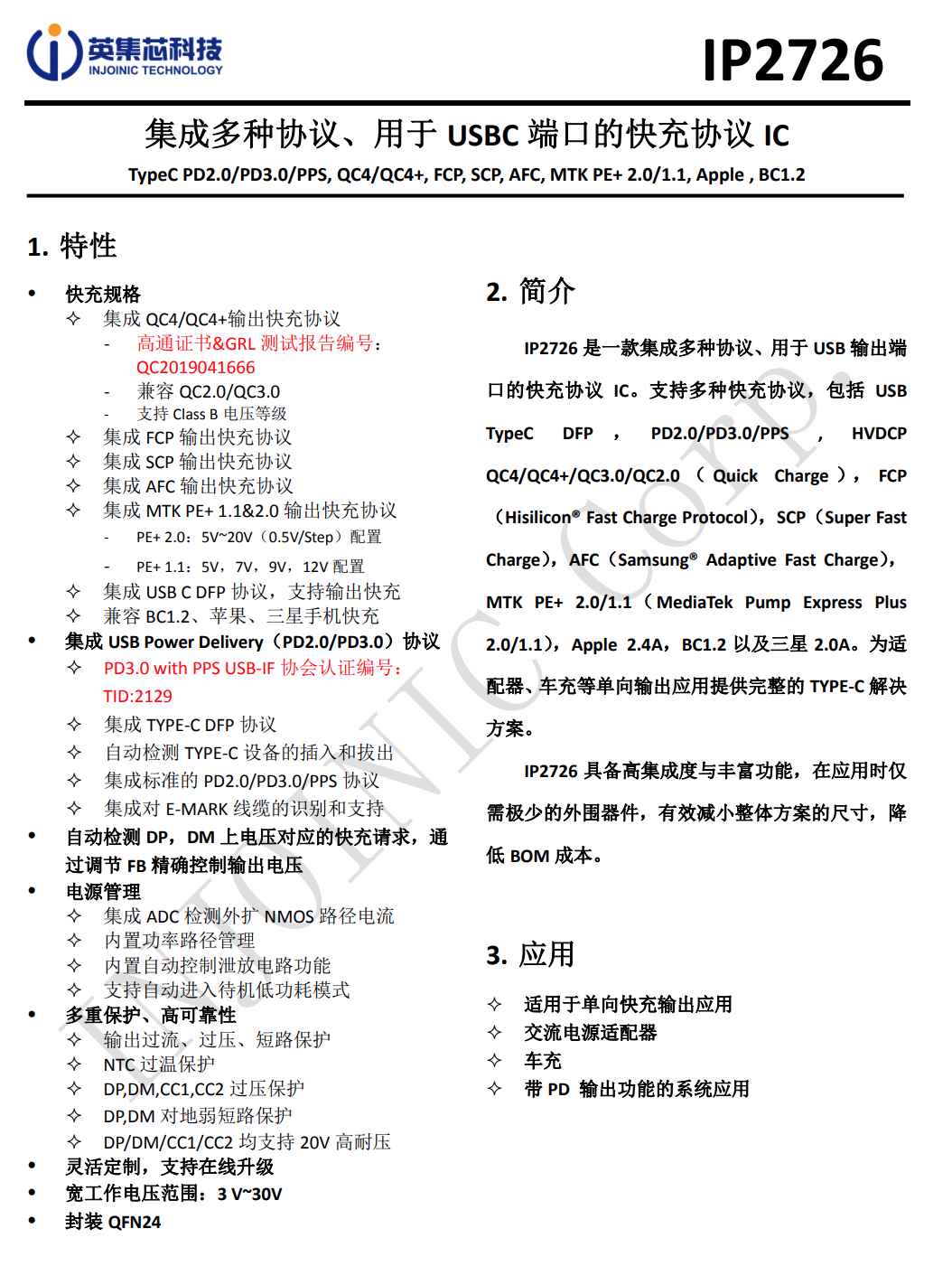
Here is the information about INJOINIC IP2726.
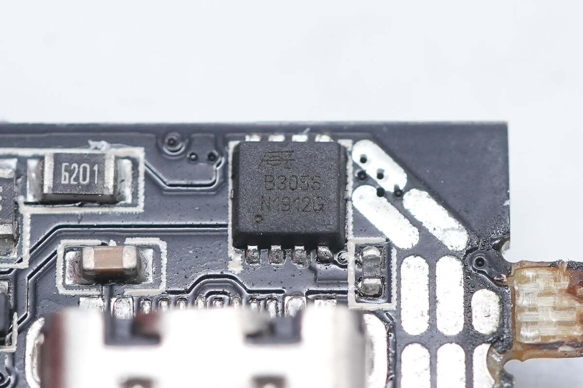
The VBUS MOSFET for output is from Fetek and adopts PRPAK3*3 package. 30V 3.9mΩ. Model is FKBB3056.
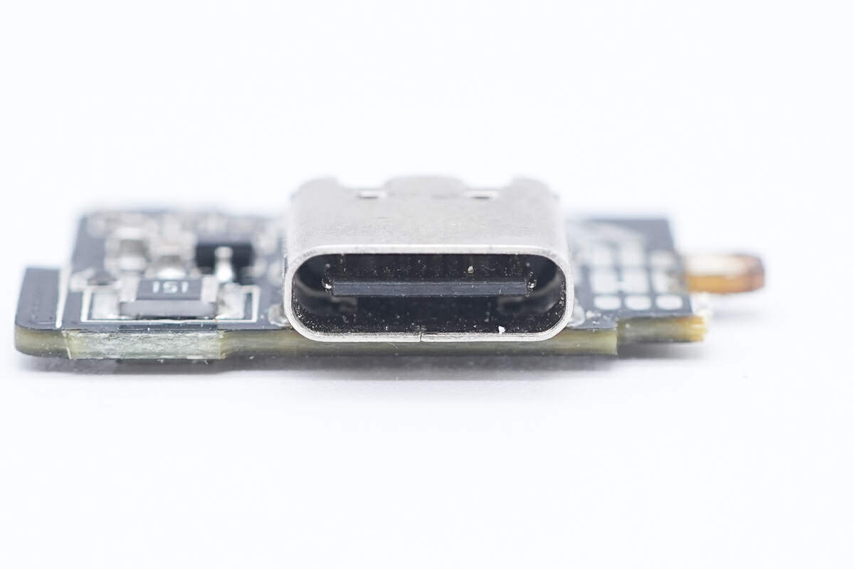
The USB-C socket has a black plastic sheet.
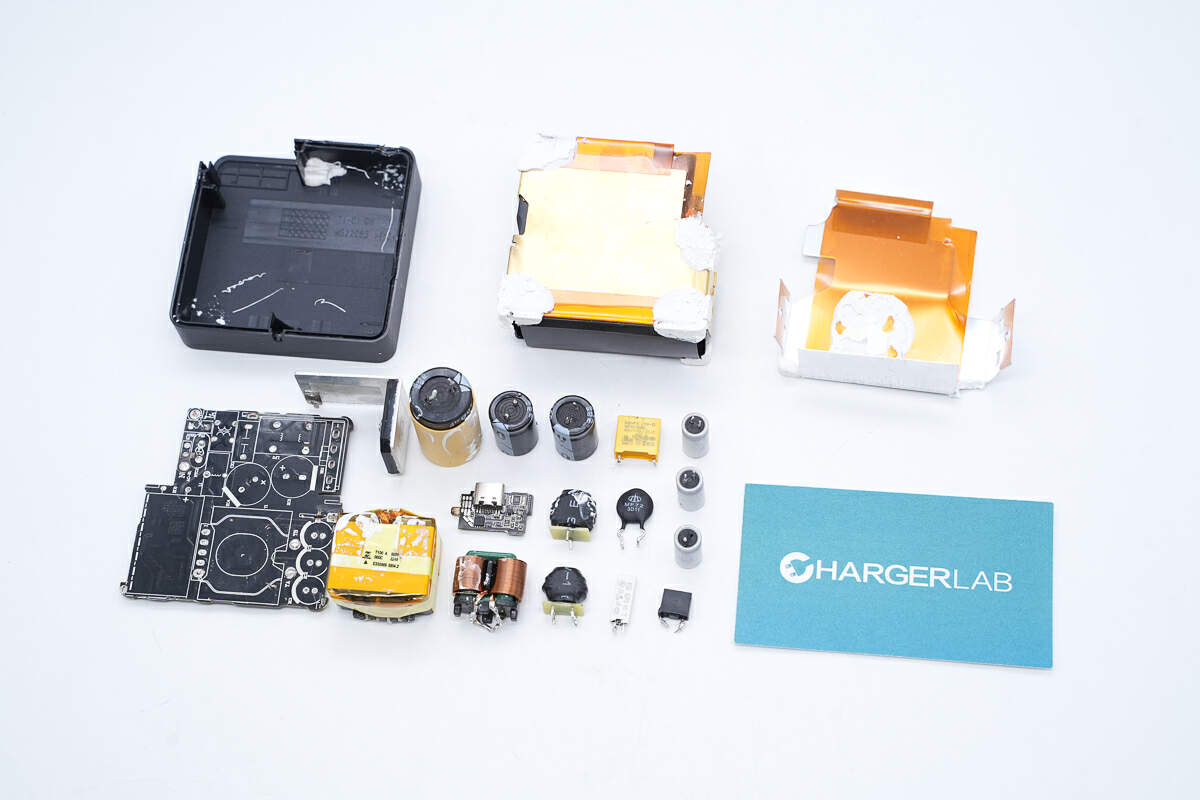
Well, those are all components of the HP 96W USB-C GaN Charger.
Summary of ChargerLAB
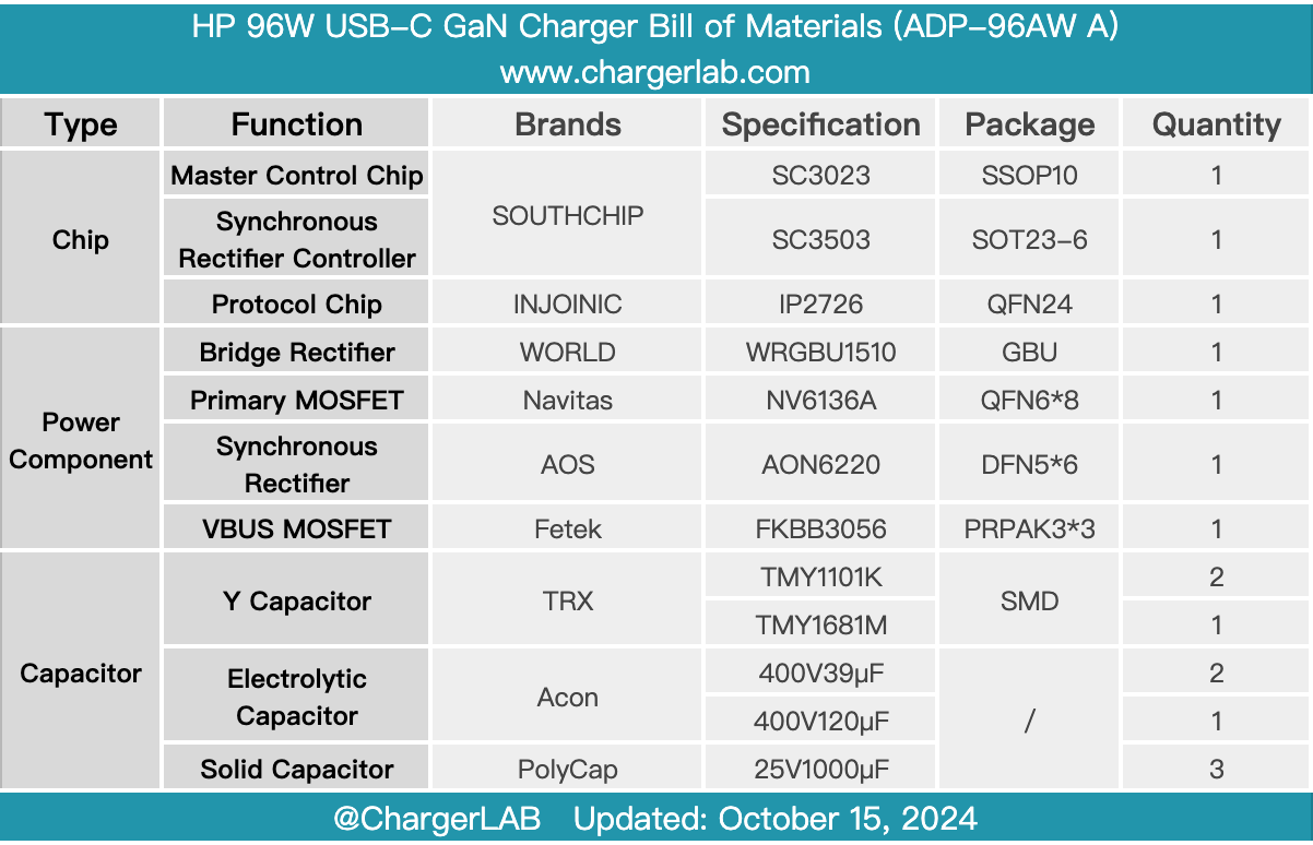
Here is the component list of the HP 96W USB-C GaN Charger for your convenience.
Its shell is black with a matte design, equipped with a foldable plug and a USB-C port. The charger supports an input range of 100-240Vac. It has a maximum output power of 96W.
After taking it apart, we found it adopts QR flyback topology. The main components it uses are from well-known brands. The gaps between components are reinforced with potting compound, and the PCBA module is covered with heat sinks. The workmanship is solid.
Related Articles:
1. Teardown of Lenovo Original 100W GaN Charger for Laptops
2. Teardown of Google 45W GaN Power Adapter
3. Teardown of Anker Prime 200W 6 Ports GaN Charger

