Introduction
ChargerLAB recently got our hands on the HP 65W Dual USB-C GaN Power Adapter. It has two USB-C output ports, which can provide up to 65W individually, and supports PPS fast charging. That means it's compatible with laptops and phones. Next, we gonna take it apart to check its internal components and structure.
Product Appearance
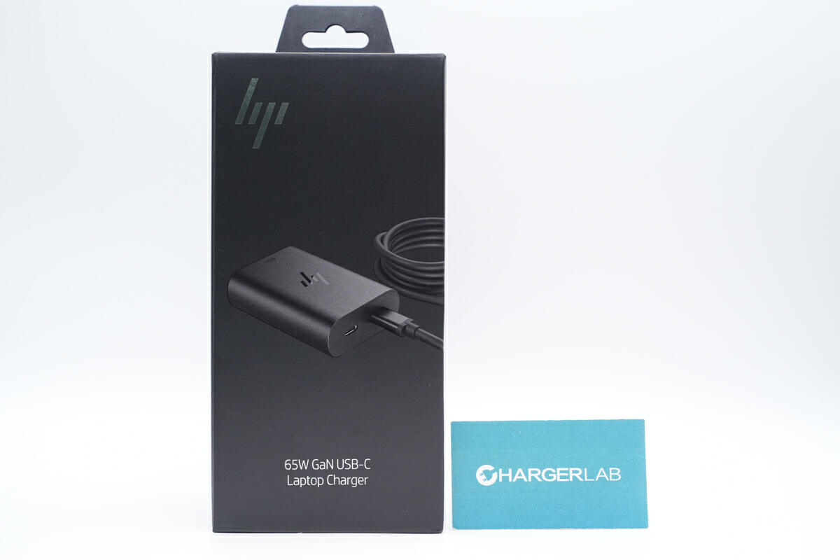
The HP brand and product name are printed on the front of the box, and the product looks very mysterious under the black background.
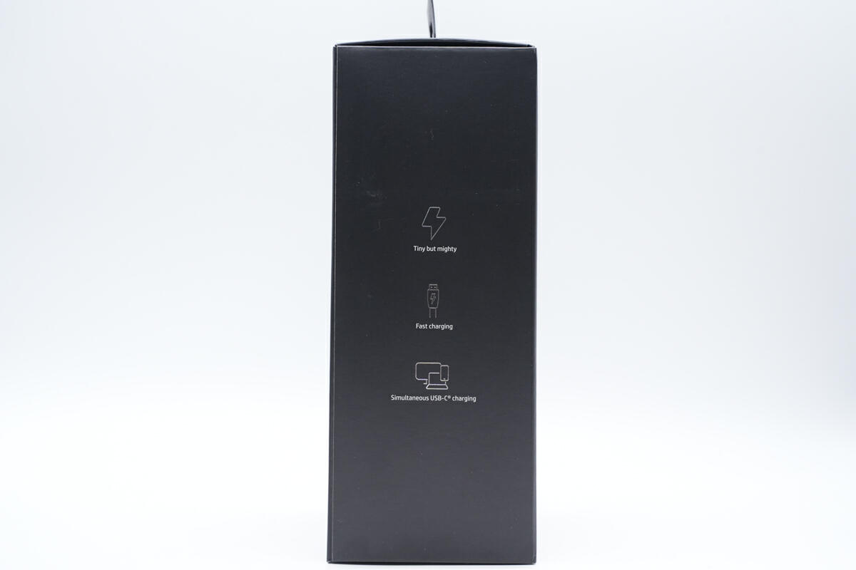
They're three major selling points on one side.
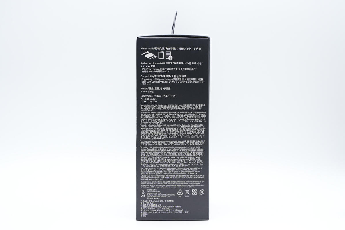
And specs info is on the other side. It shows China HP Co., Ltd is the general agent and Delta Electronics, Inc is the manufacturer.
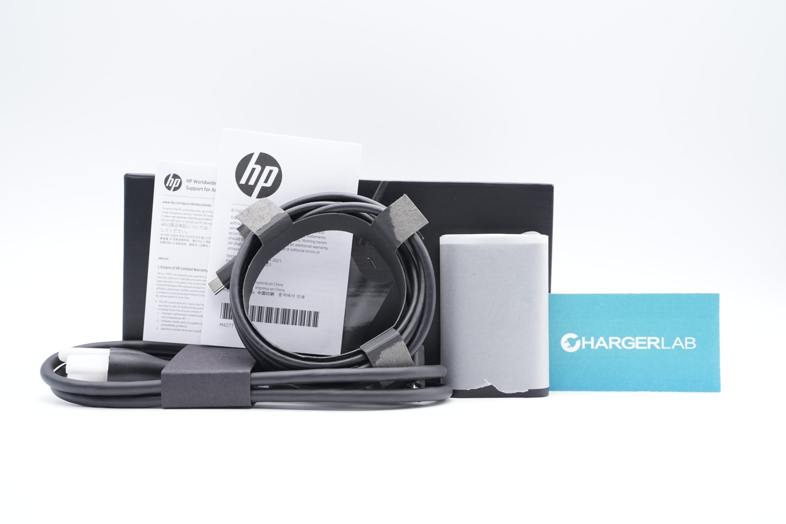
The box contains the power adapter, power cord, dual USB-C cable, and instruction manual.
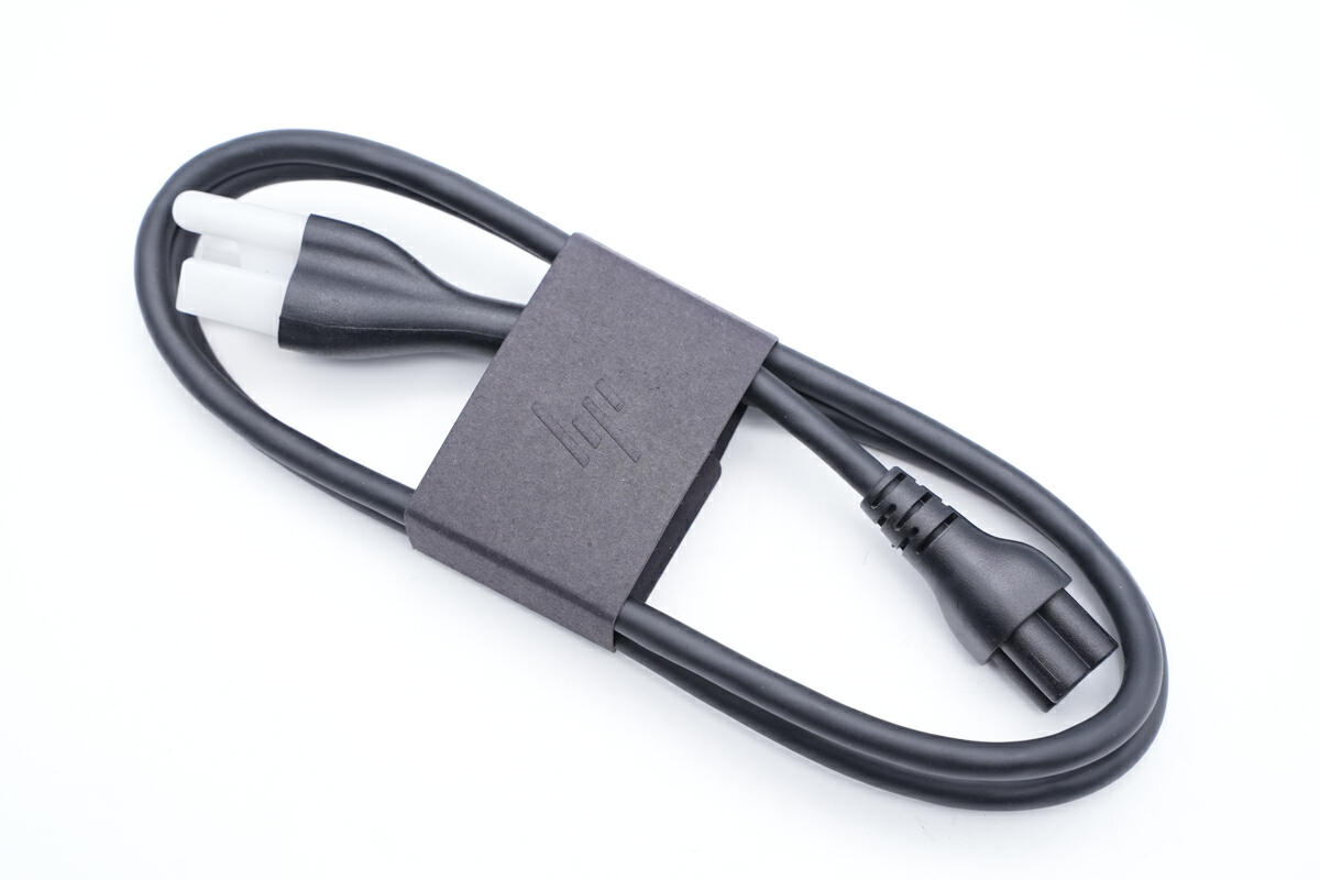
The power cord is fixed with HP customized cardboard, and the input plug is protected by a cap.
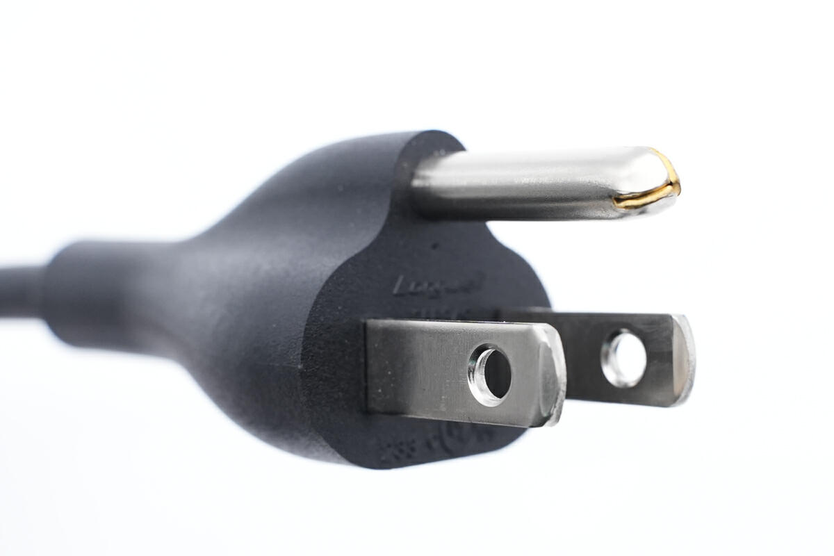
This is a US plug.
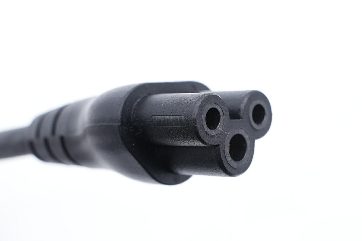
And this is the output end.
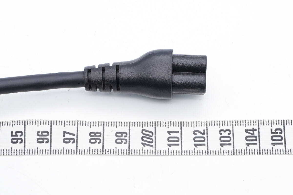
The length of the power cord is about 1.02m (3' 4.2").
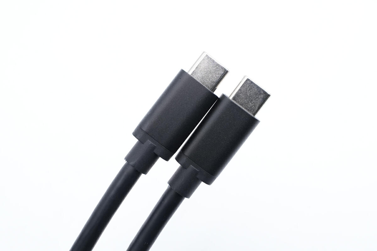
The dual USB-C cable adopts black matte design.
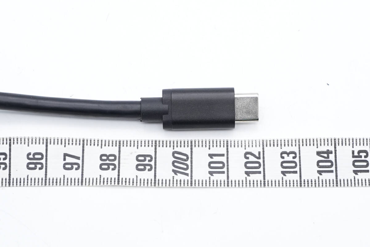
Length is also about 1.02m (3' 4.2").
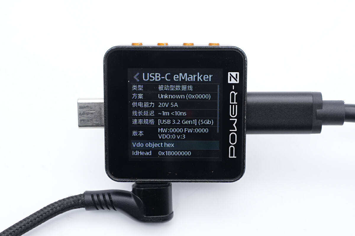
ChargerLAB POWER-Z KM002C shows it's a USB 3.2 Gen1 (5Gbps) cable with an E-Marker chip inside.
And it also supports 20V5A 100W.
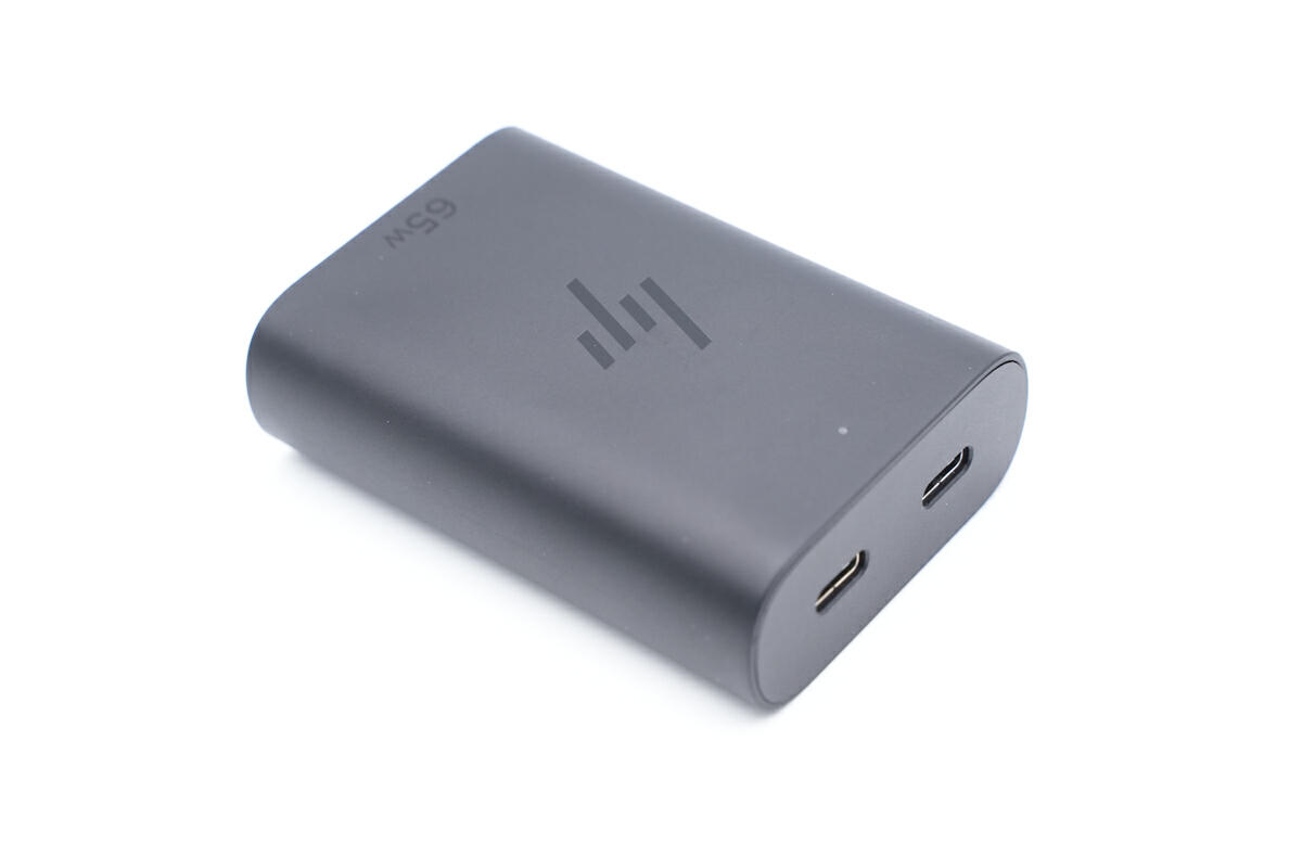
It adopts a classic HP curved design.
And the matte shell can reduce fingerprints.
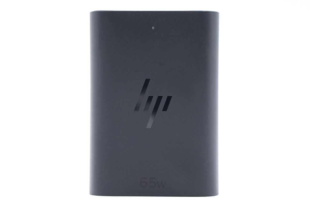
A big HP brand is in right in the middle.
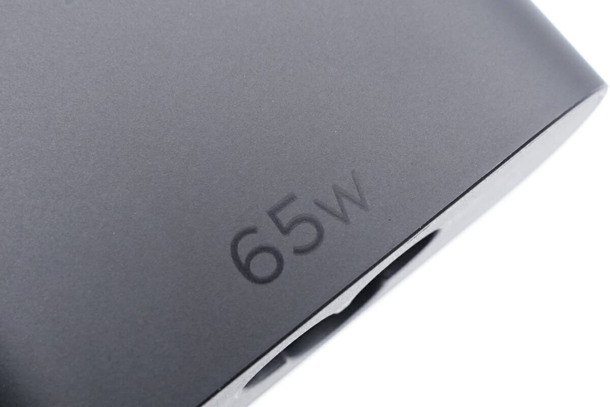
And a "65W" is engraved on the input end.
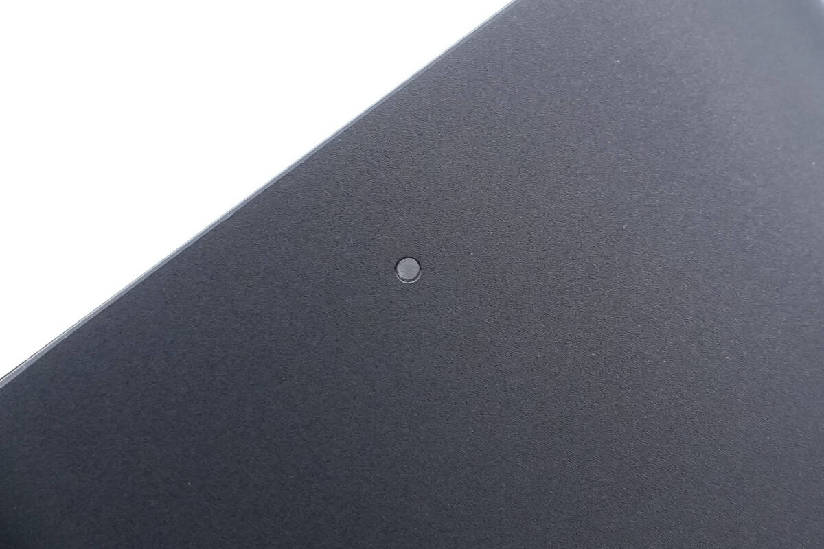
Here is an indicator light for the charging status.
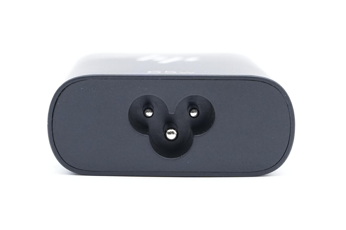
The grounding prong inside the input socket can protect the user from electric shock.
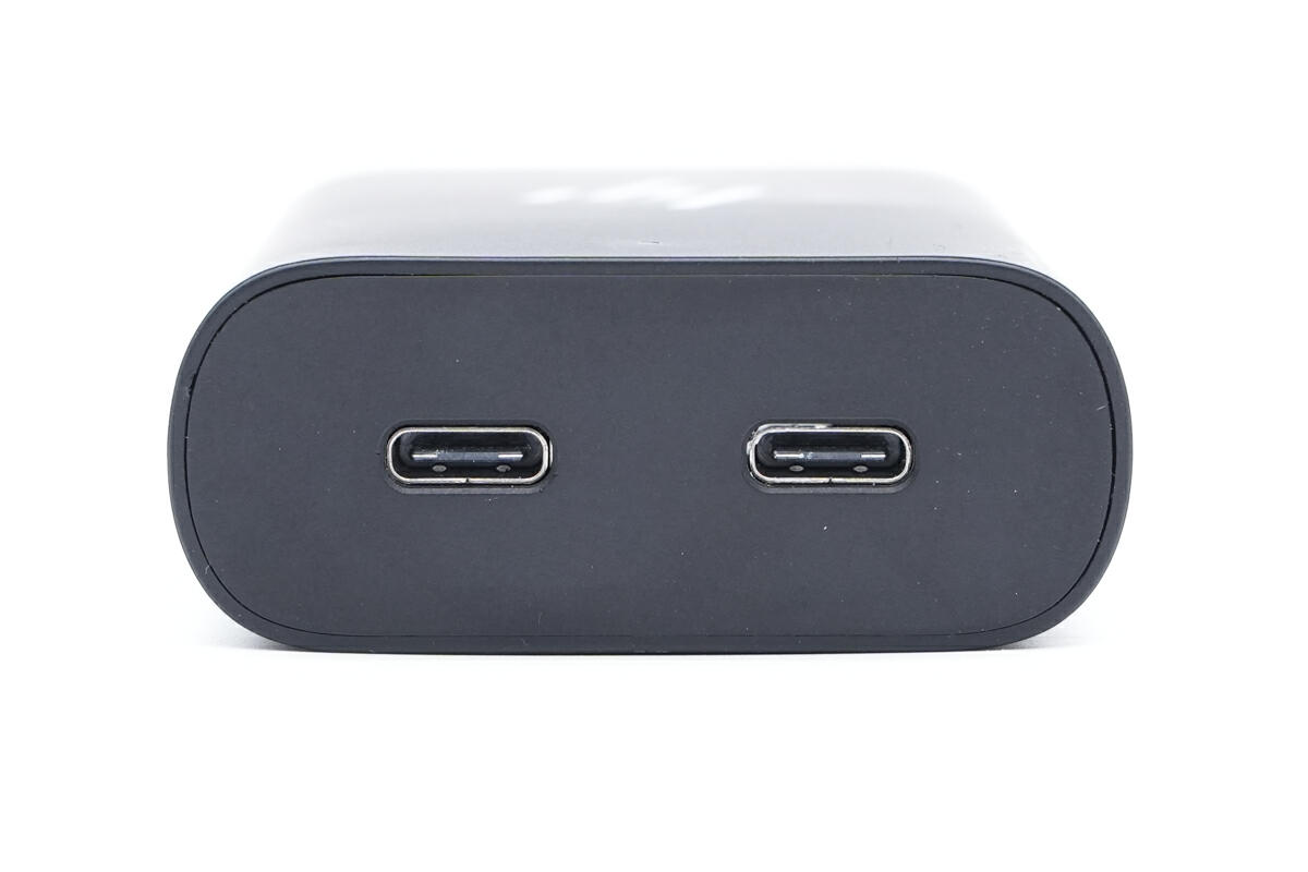
It adopts two USB-C ports.
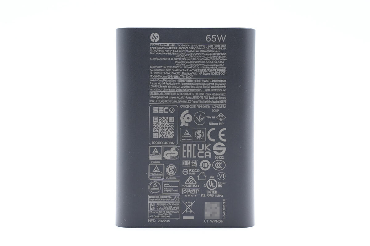
The specs info is printed on the bottom.
Model is TPN-DA27. It can support input of 100-240V~50/60Hz 1.7A. The USB-C1/C2 can support up to 65W. When using two ports at the same time, the power can be divided into 45W, 20W or 30W,30W. The manufacturer is Delta. And it has passed CCC, CP, CE, PSE, EAC, GS, TUV, UKCA, NOM, NYCE, UL certifications.
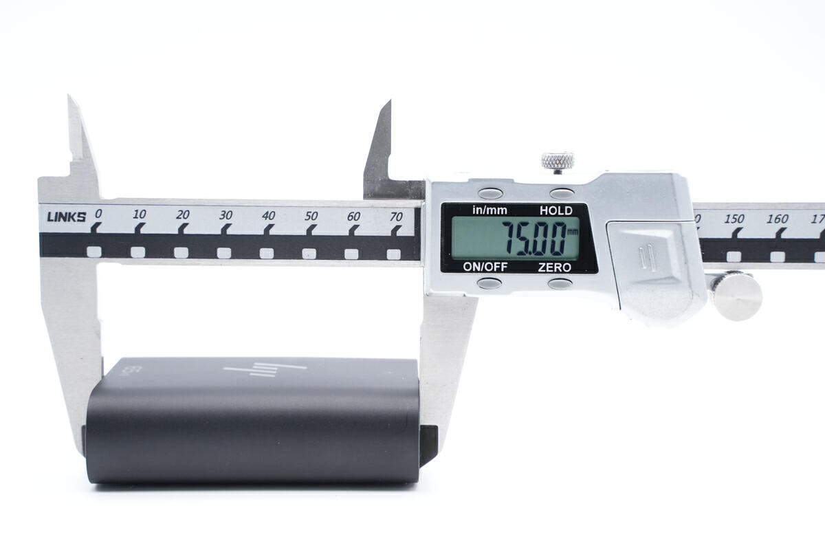
The length is about 75mm (2.95 inches).
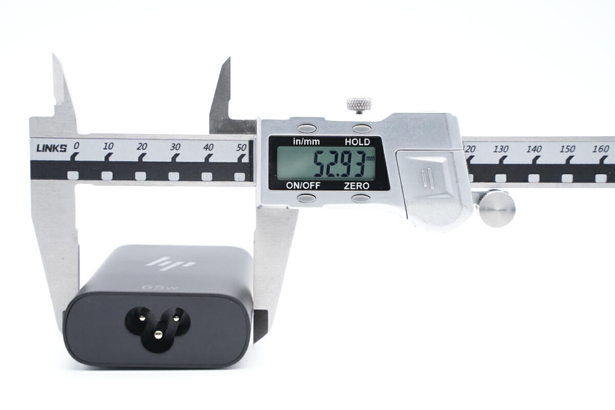
The width is about 53mm (2.09 inches).
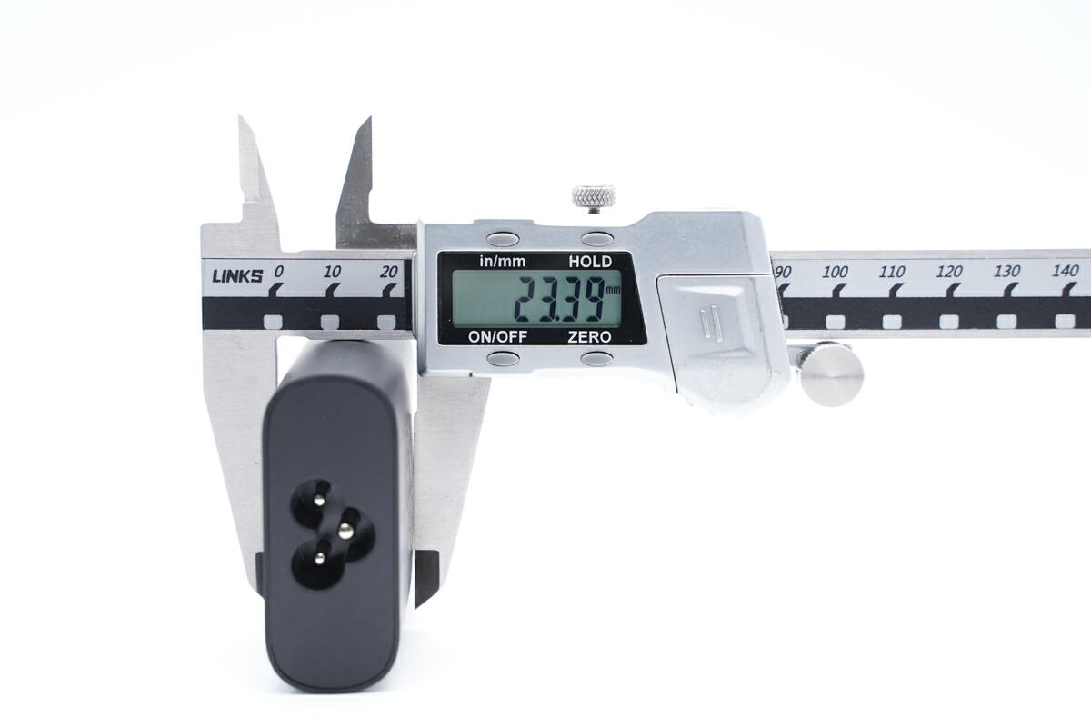
And the height is about 23.4mm (0.92 inches).
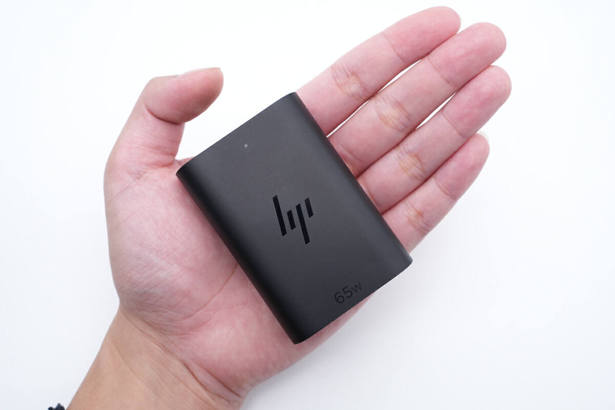
It looks pretty small in my hand.
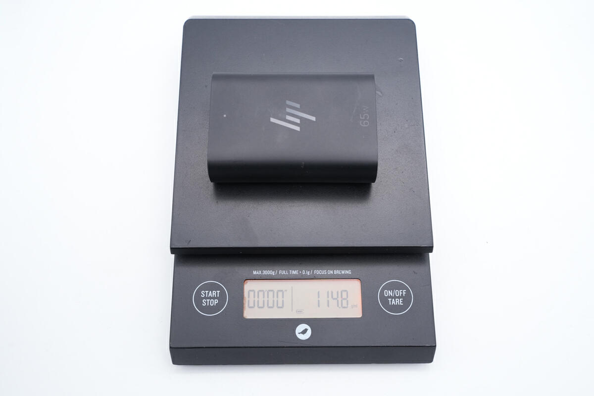
The weight of the power adapter is about 115g (4.06 oz).
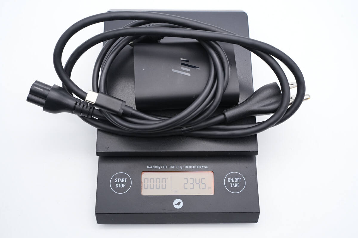
Including those two cables, the total weight has increased to about 235g (8.29 oz).
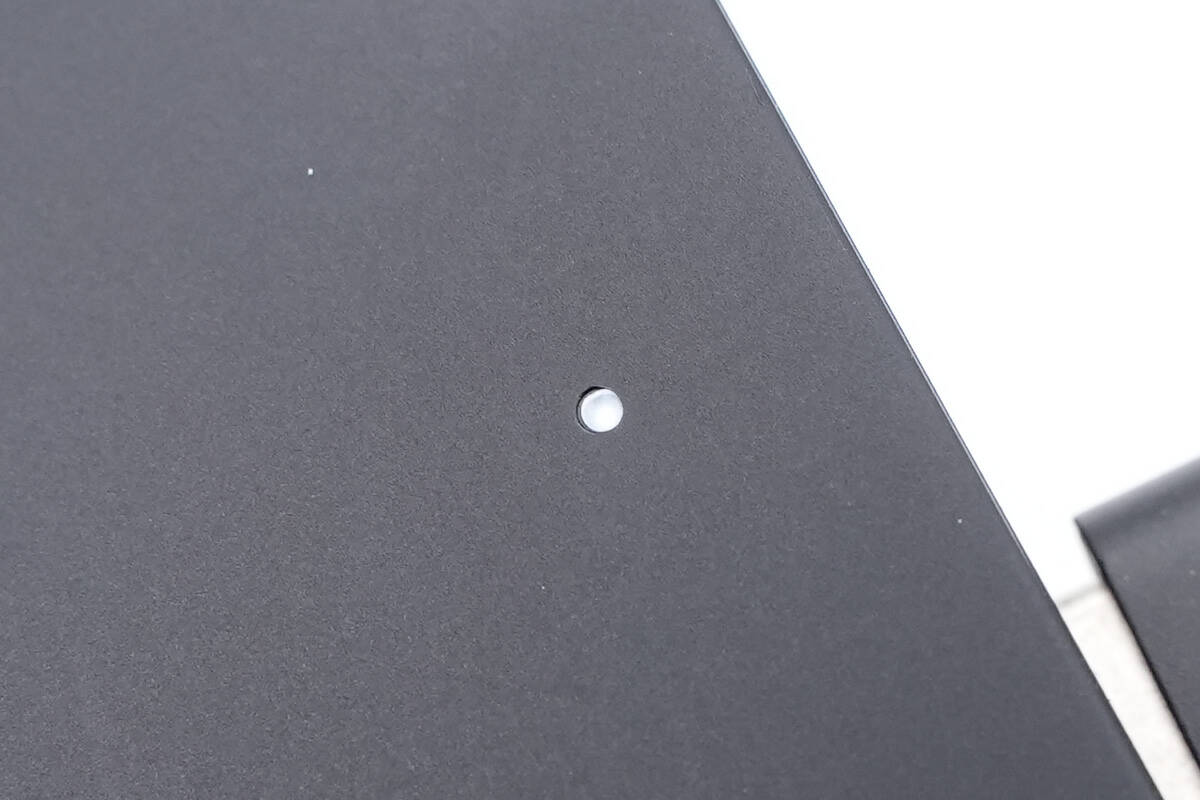
The indicator lights up when powered on.
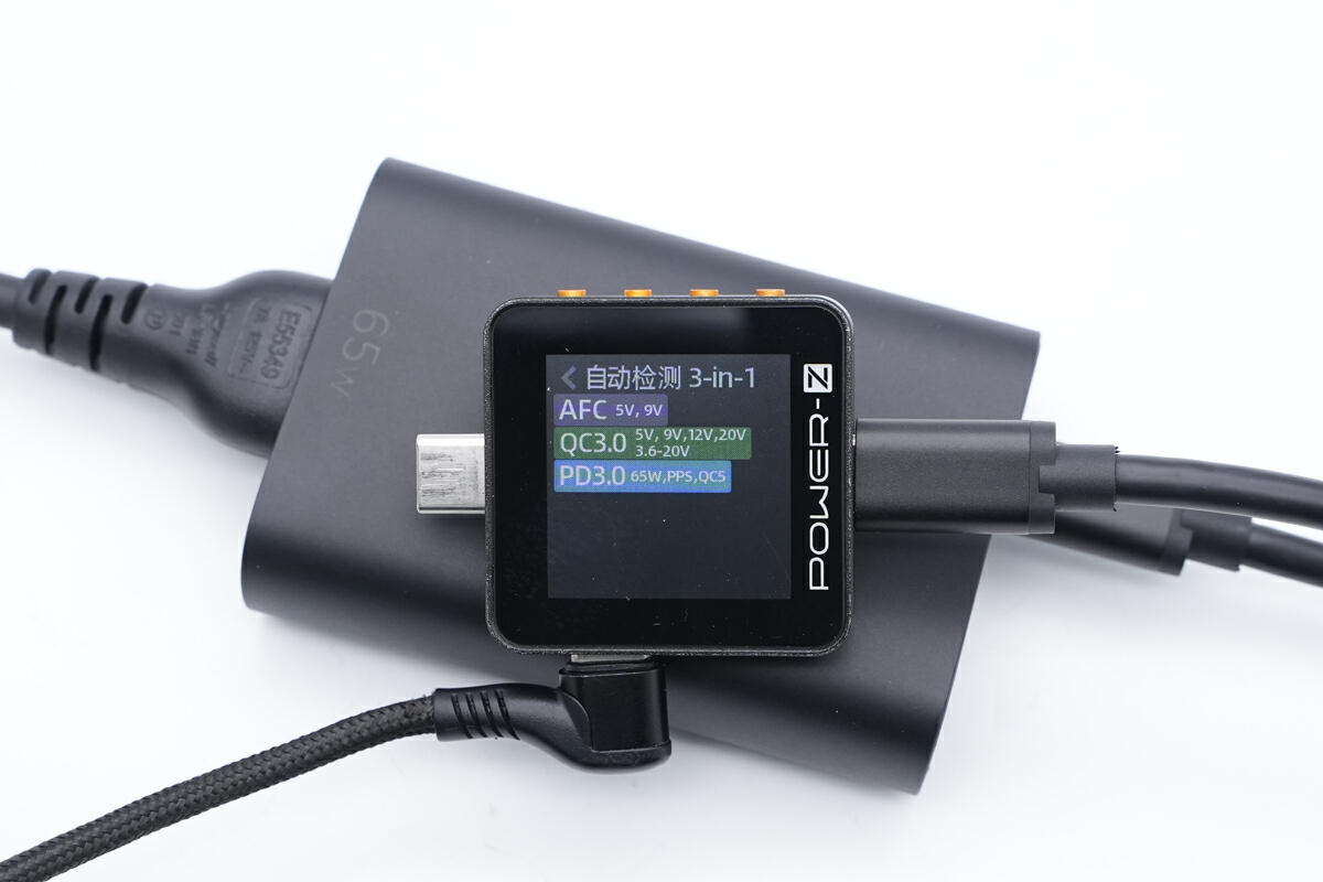
ChargerLAB POWER-Z KM002C shows the USB-C1 supports AFC, QC3.0/5, PD3.0, and PPS protocols.
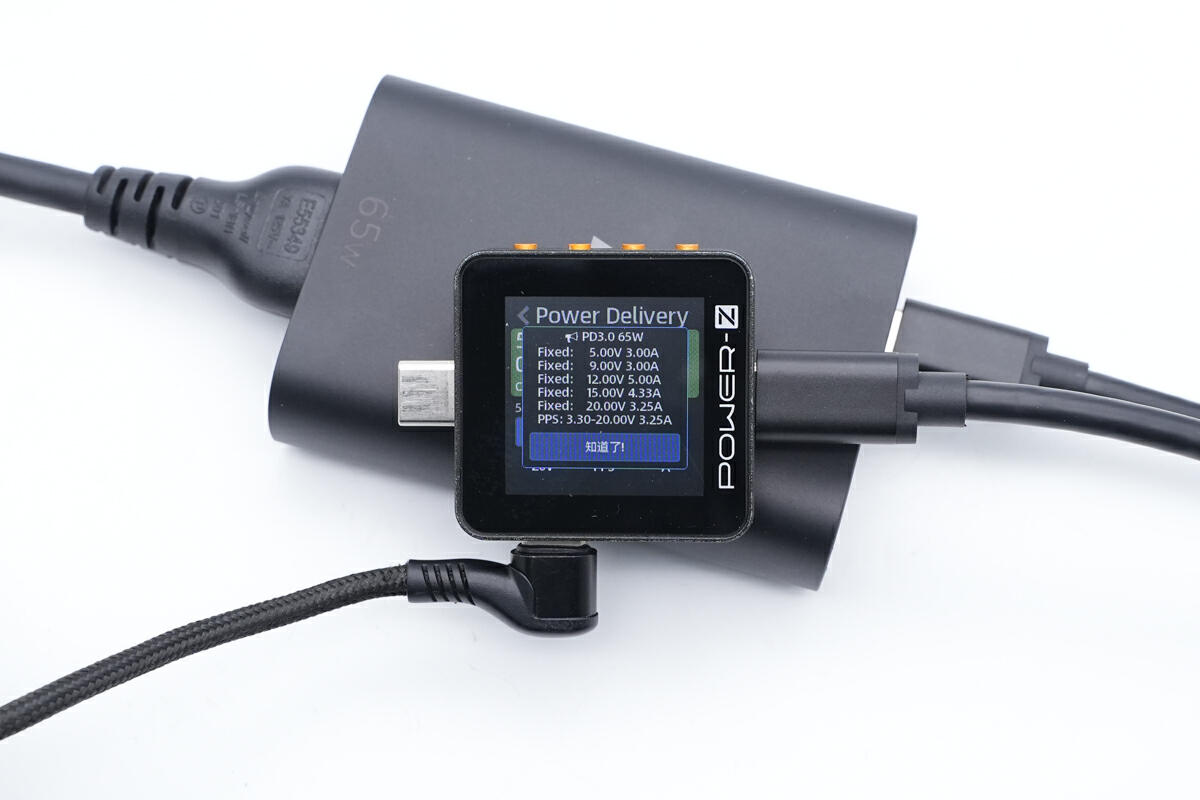
And it also supports five fixed PDOs of 5V3A, 9V3A, 12V5A, 15V4.33A, 20V3.25A, and a set of PPS.
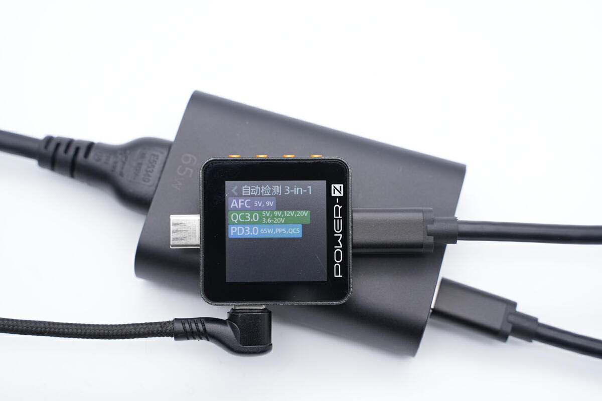
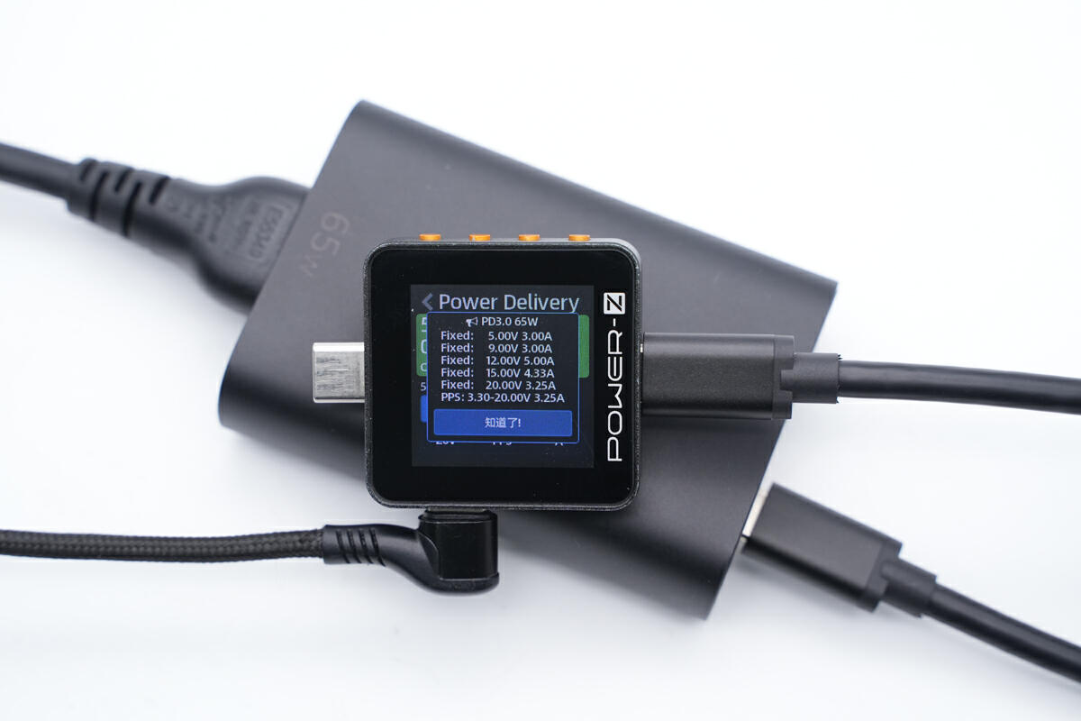
The supported protocols and PDOs of USB-C2 are the same as USB-C1. So, both can support up to 65W.
Teardown
Next, we gonna take it apart to check out the internal components and structure.
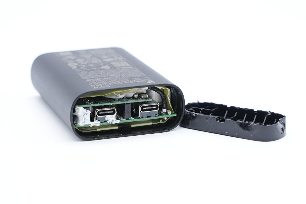
Firstly, pry along the gap near the output panel and open it up.
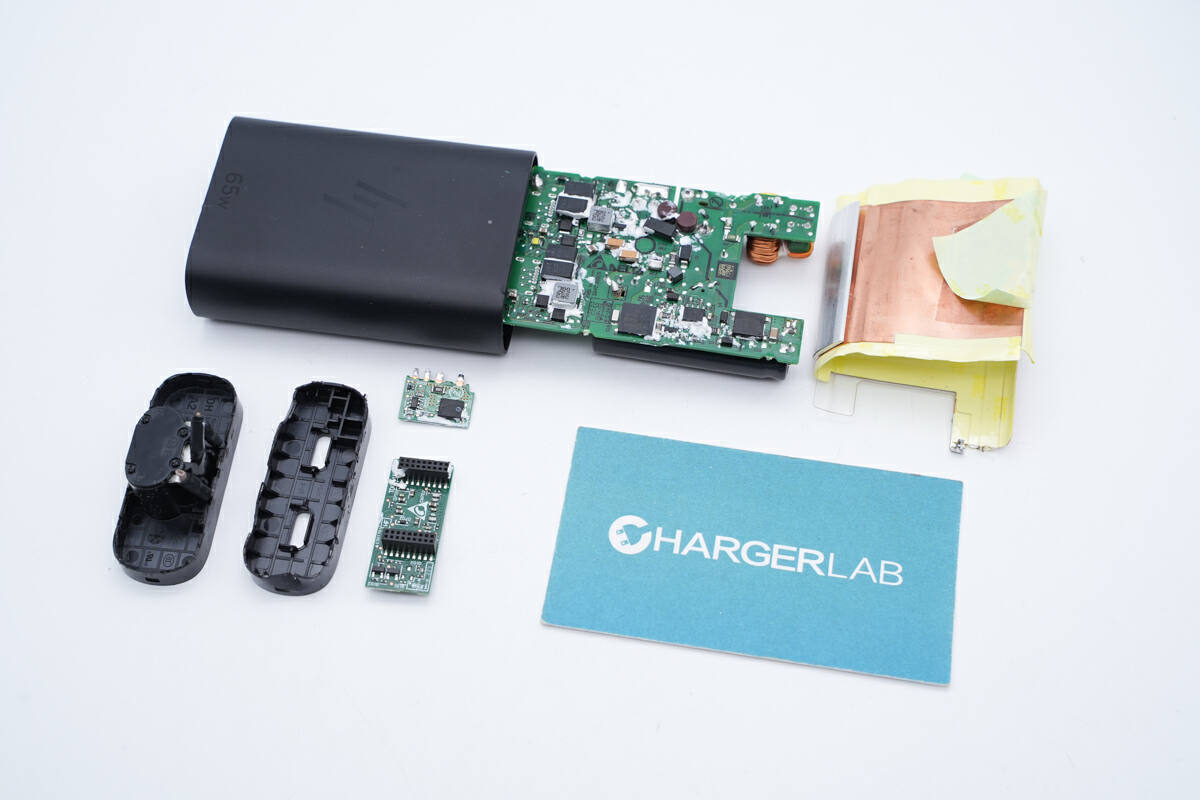
Then remove the input panel and take out the PCBA module.
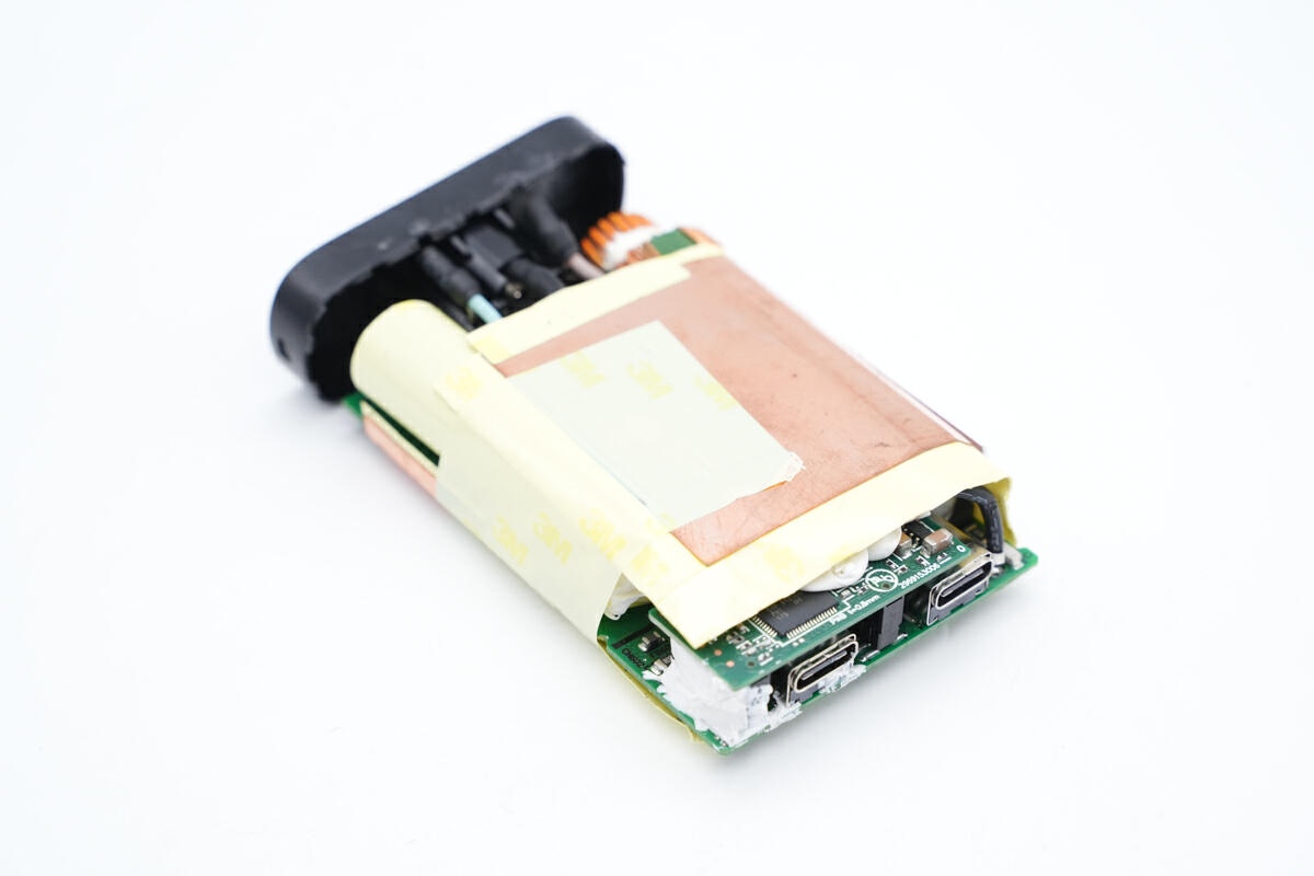
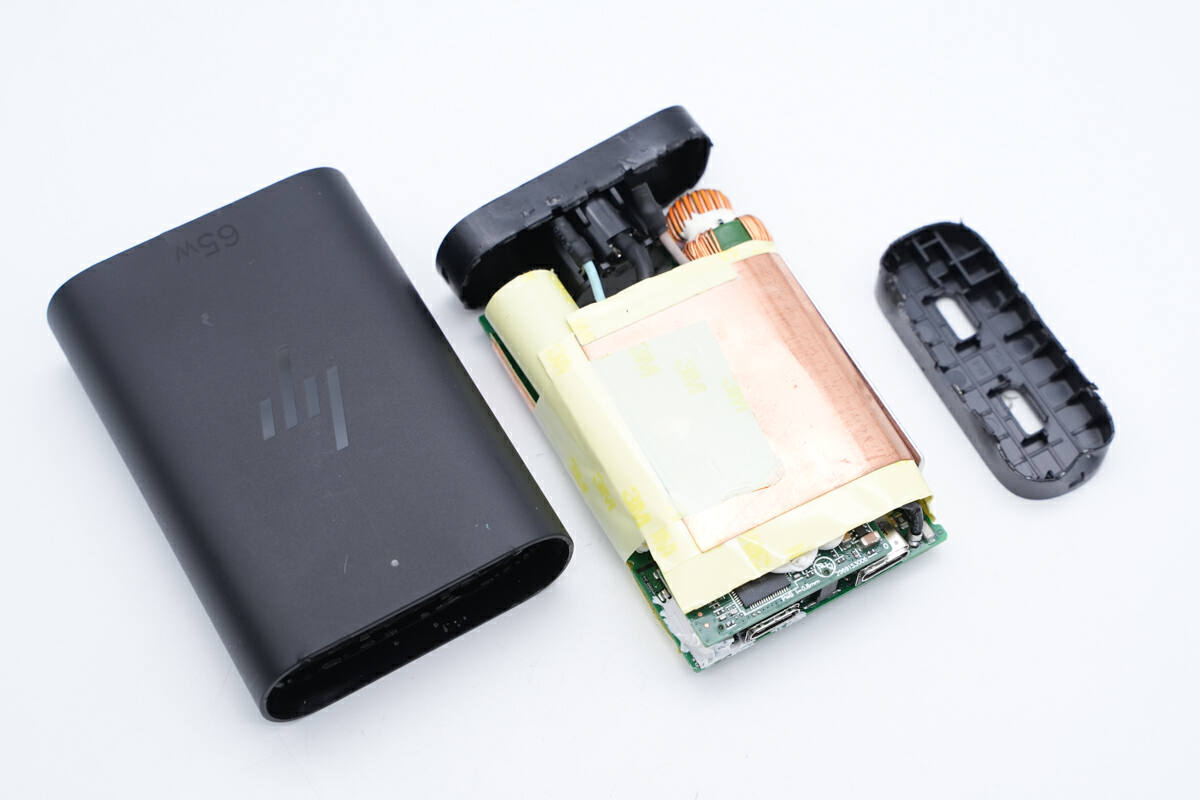
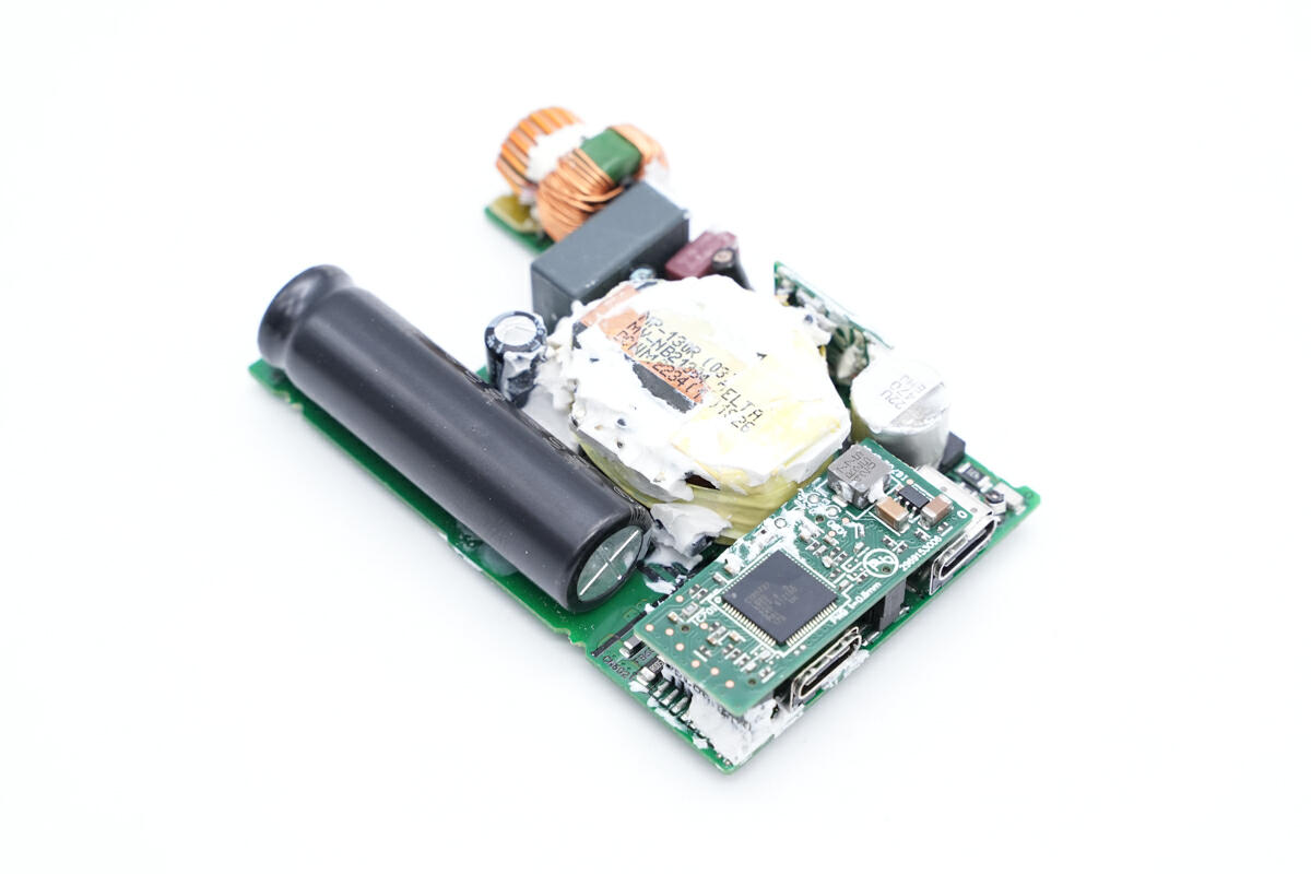
The PCBA module is wrapped with copper sheet for heat dissipation and insulated with tapes.
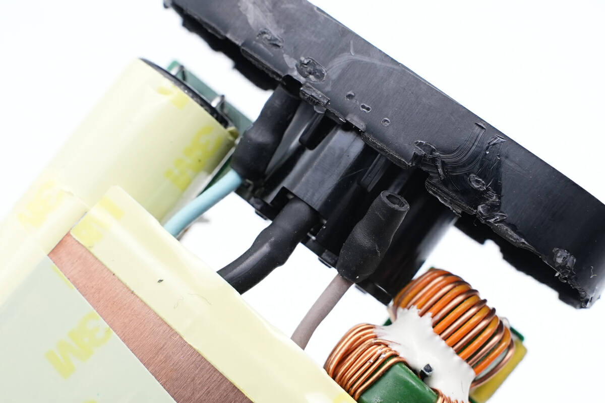
The junctions between the input wires and panel are insulated with heat-shrinkable tube.
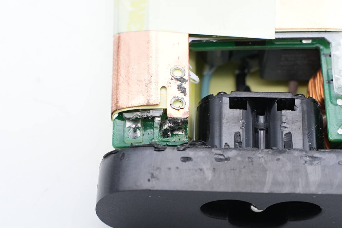
The heat sink is soldered on the PCBA module.
Close-up of the other solder joint.
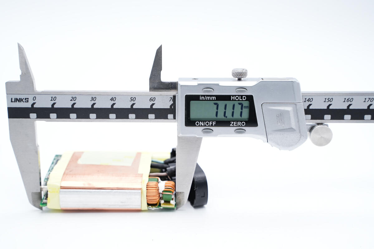
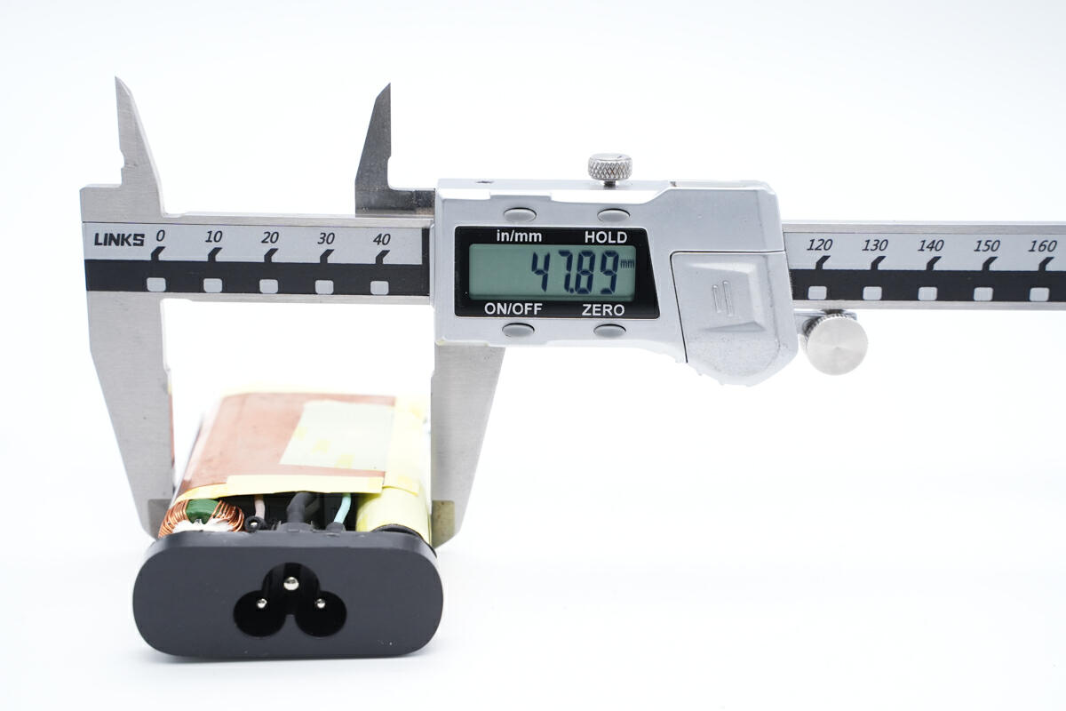
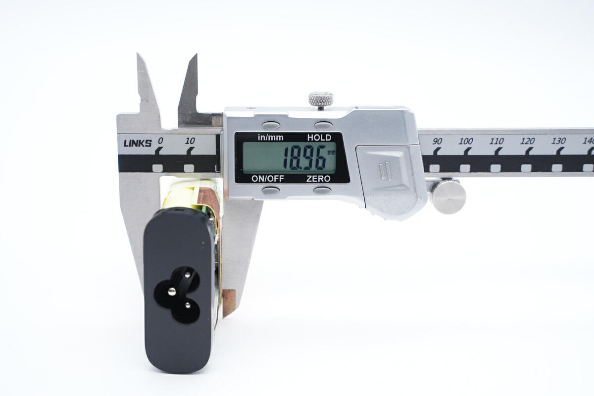
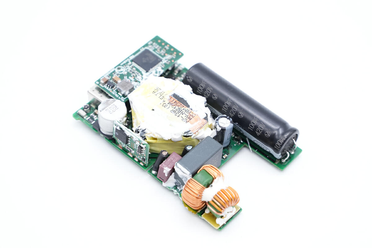
The size of the PCBA module is about 71 x 47.9 x 19mm (2.84 x 2.42 x 1.15 inches).
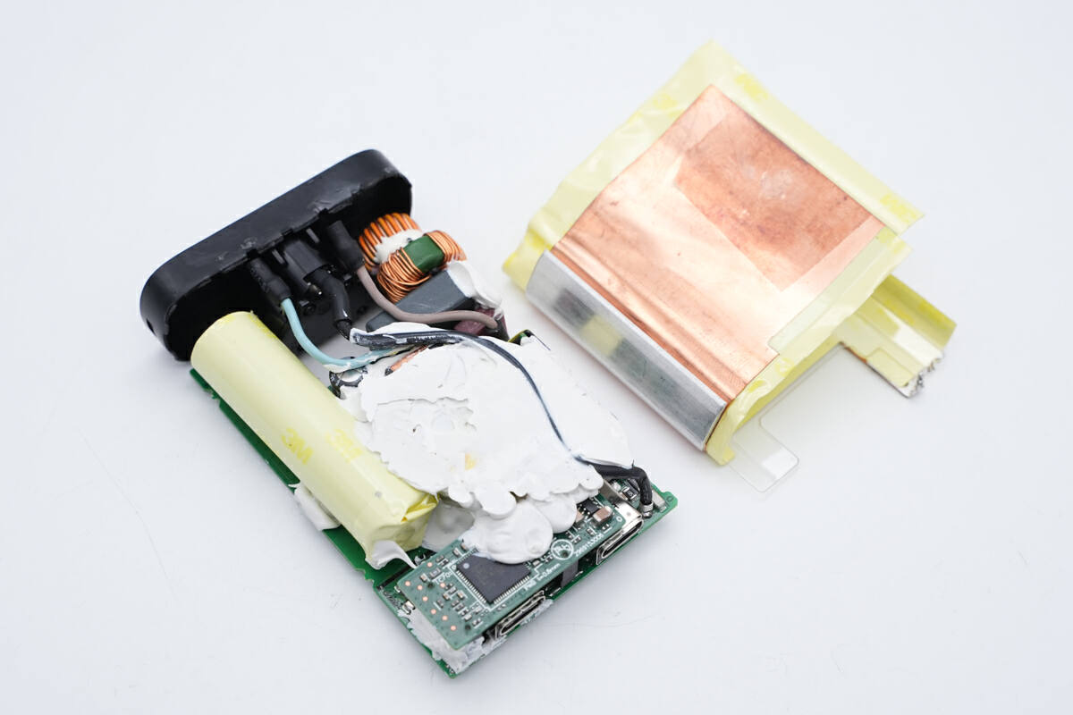
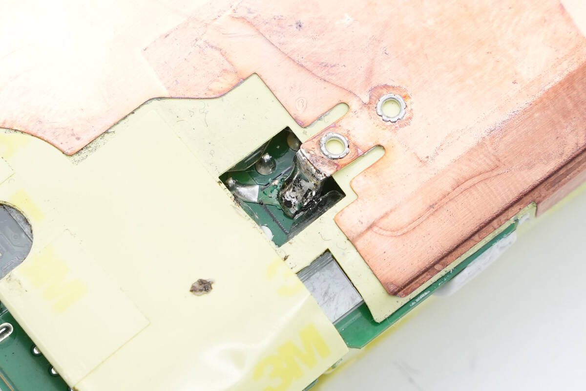
Remove all the tapes and copper sheet.
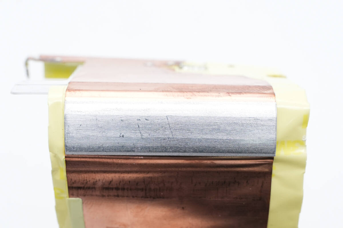
The copper sheet is filled with aluminum at the bend.
This huge electrolytic capacitor for input filtering is insulated with tape. And the transformer is fixed with a large number of silicone adhesives to dissipate heat.
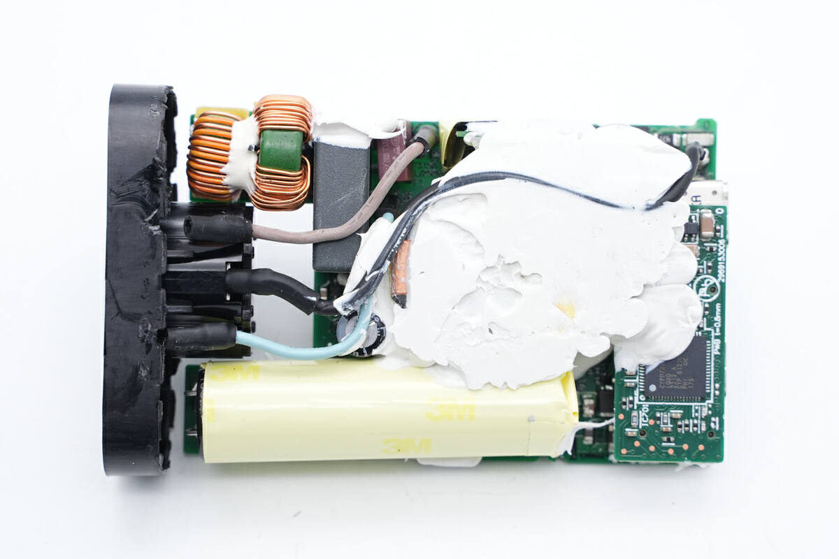
The back of the PCBA module is also fixed with a lot of silicone adhesives. They're mainly used to dissipate heat for the heating components.
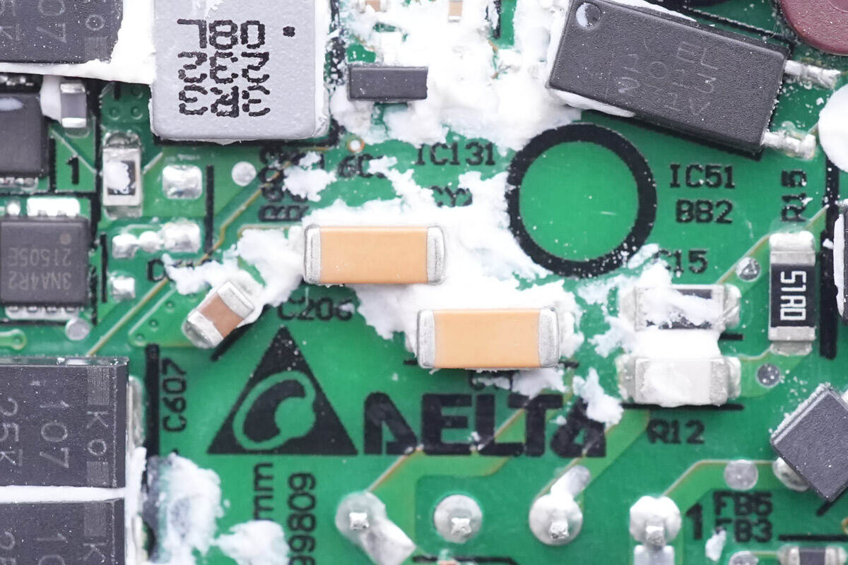
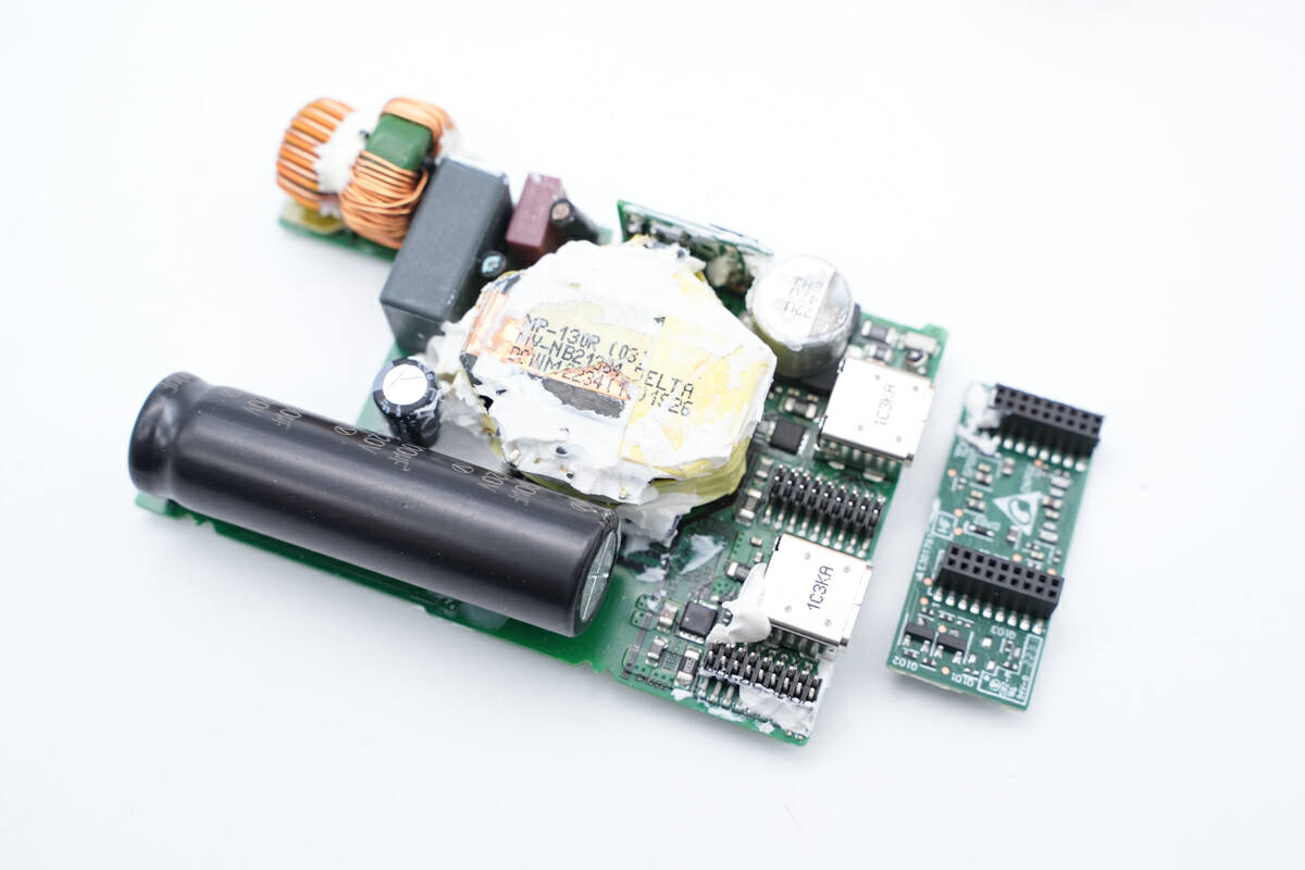
Clean off the silicone adhesives. We can see two small PCBs around the transformer.
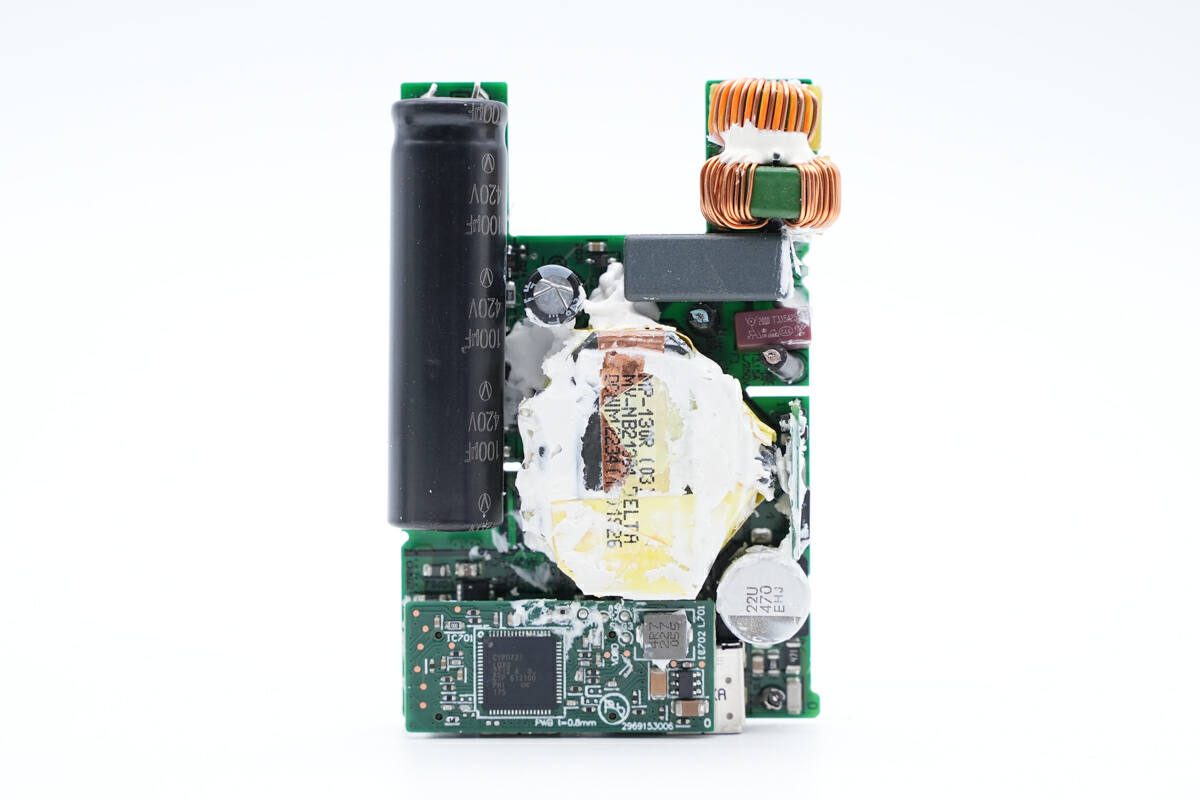
The fuse, safety X2 capacitor, common mode choke, electrolytic capacitor and transformer are on the front of the PCBA. The small PCB on the lower right is equipped with synchronous rectifier circuit, and the small PCB on the bottom is equipped with a buck circuit and protocol chip. The right side is the AC input part.
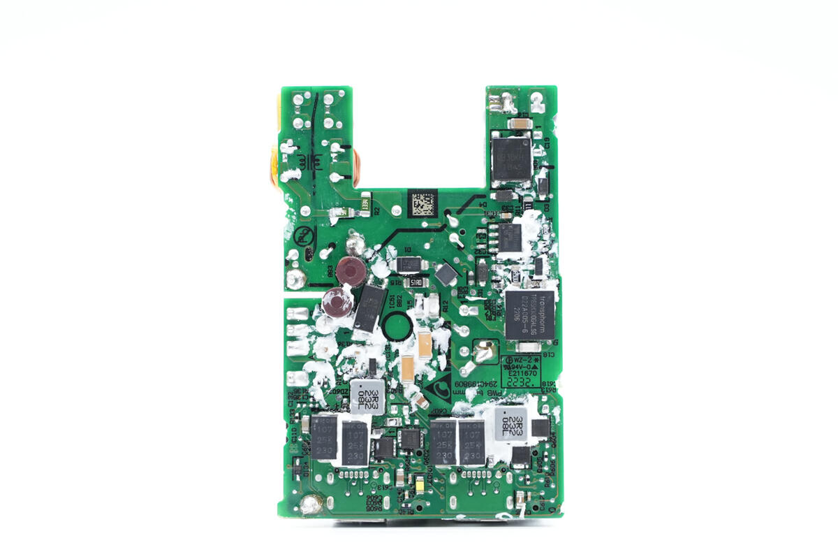
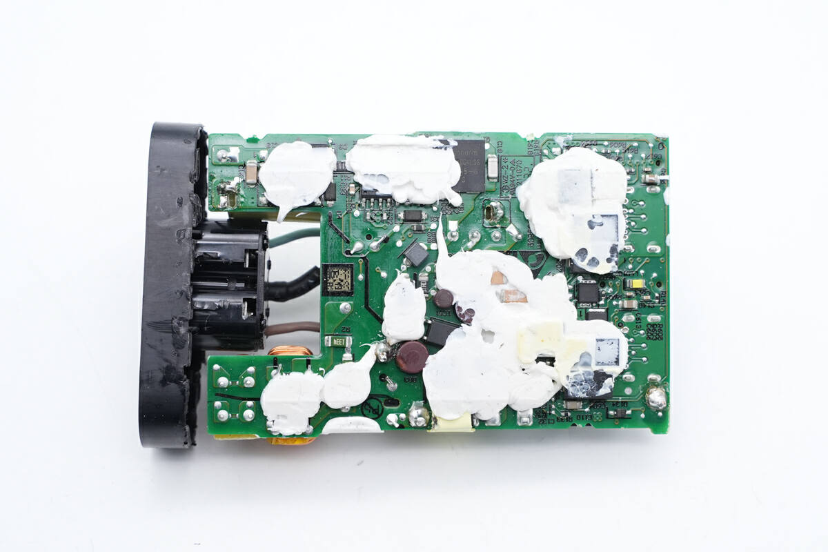
And the bridge rectifier, primary controller, GaN FET, optocoupler, two buck inductors, synchronous buck MOSFET and SMD capacitor for output filtering are on the back.
ChargerLAB found this HP 65W GaN power adapter adopts QR flyback topology. After the synchronous rectification, it can output two wide range of voltages on both ports controlled by the buck circuit inside the Infineon protocol chip.
Next, we will introduce the components from the input end.
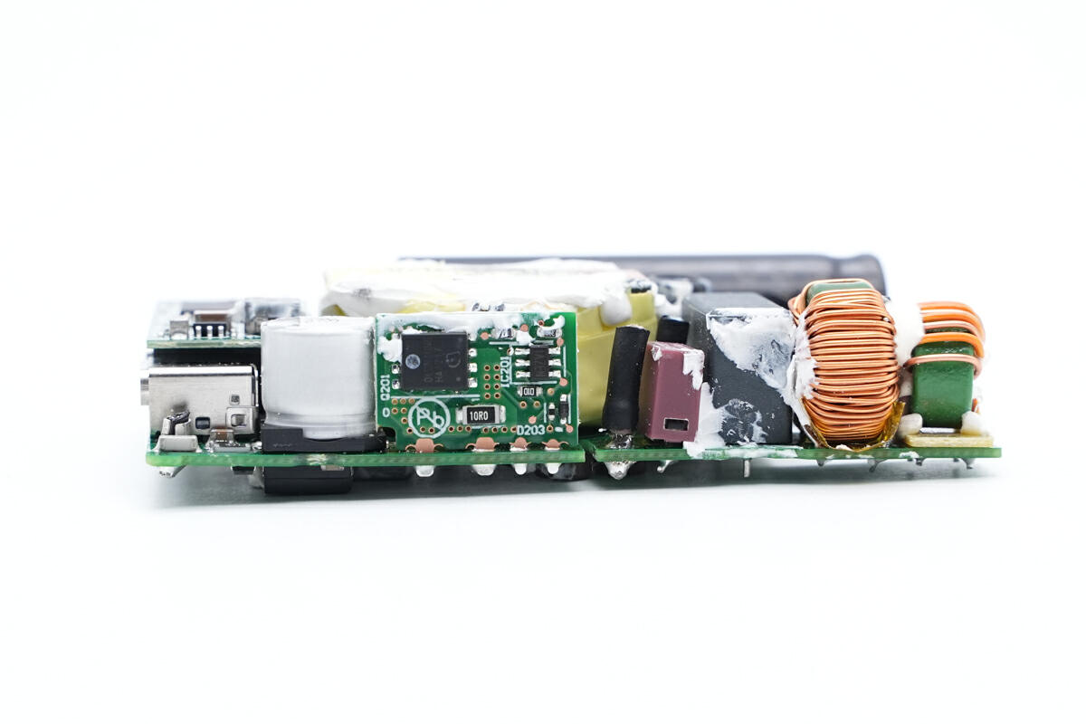
The input time-delay fuse is soldered in the middle of the PCBA module, and the small synchronous rectifier PCB is on the left.
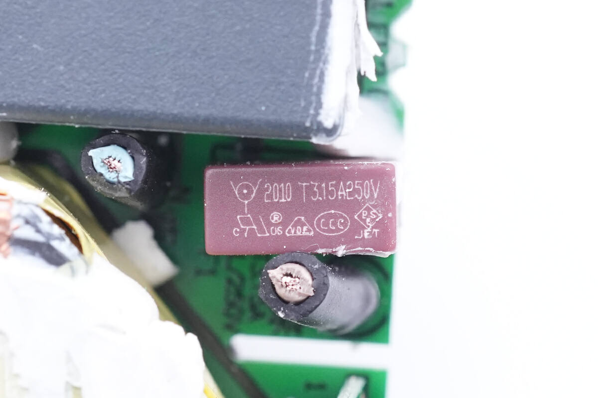
And it is from Walter Electronic. 3.15A 250V.
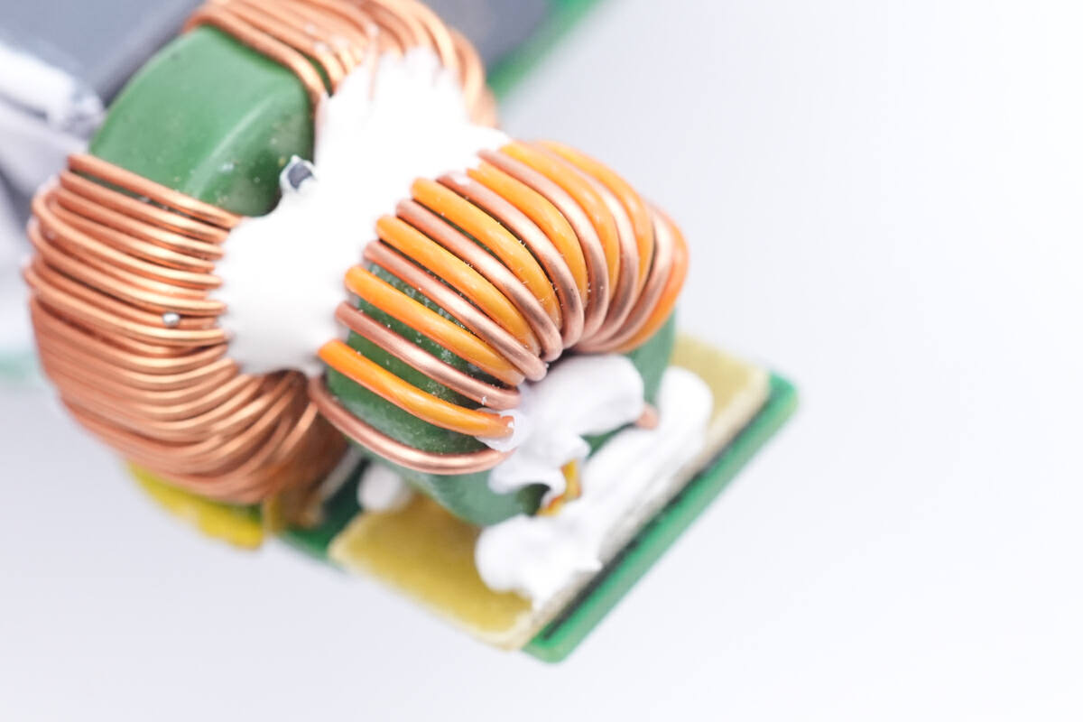
The first common mode choke is wound with magnet and insulated wires, and the lead wire is insulated with bakelite.
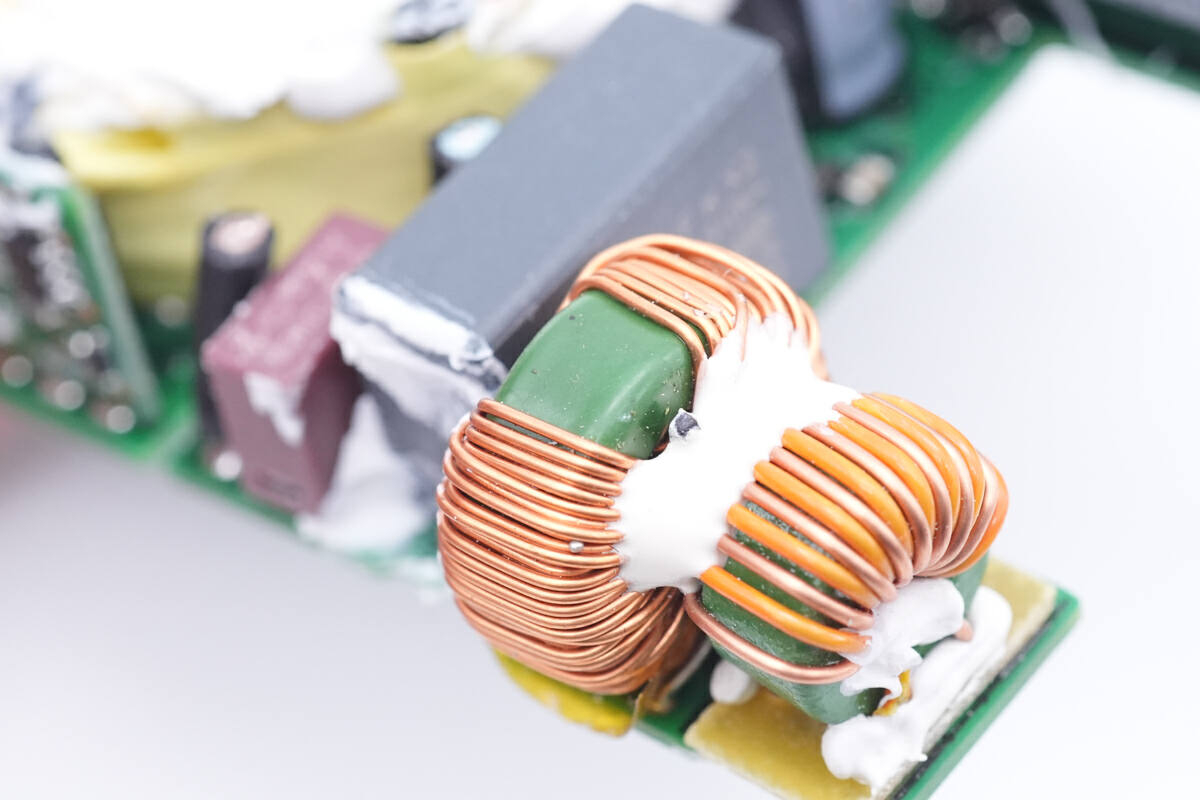
The second common mode choke is wound with magnet wires, and these two chokes are fixed with white silicone adhesives.
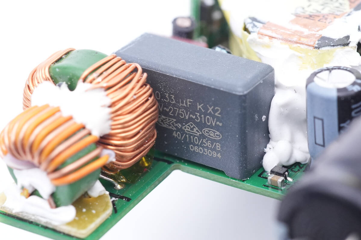
The capacitance of this safety X2 capacitor is 0.33μF.
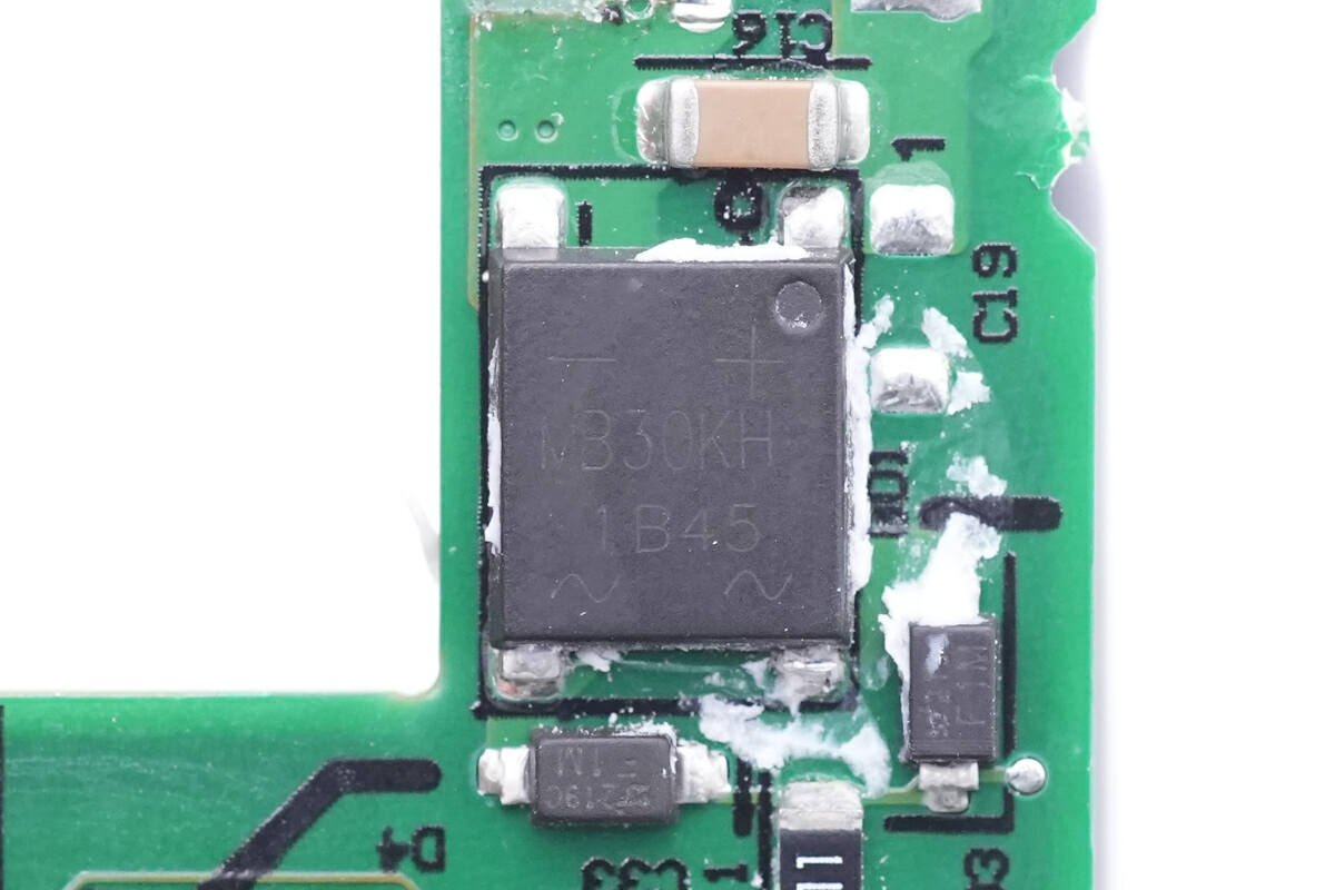
This bridge rectifier's model is MB30KH, and it can support input of 3A.
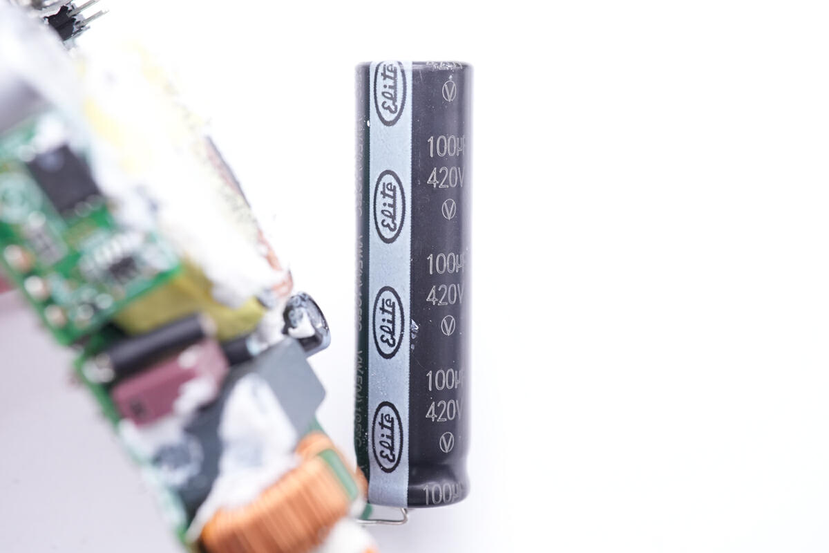
This huge electrolytic capacitor for input filtering is from Chinsan. 100μF 420V.
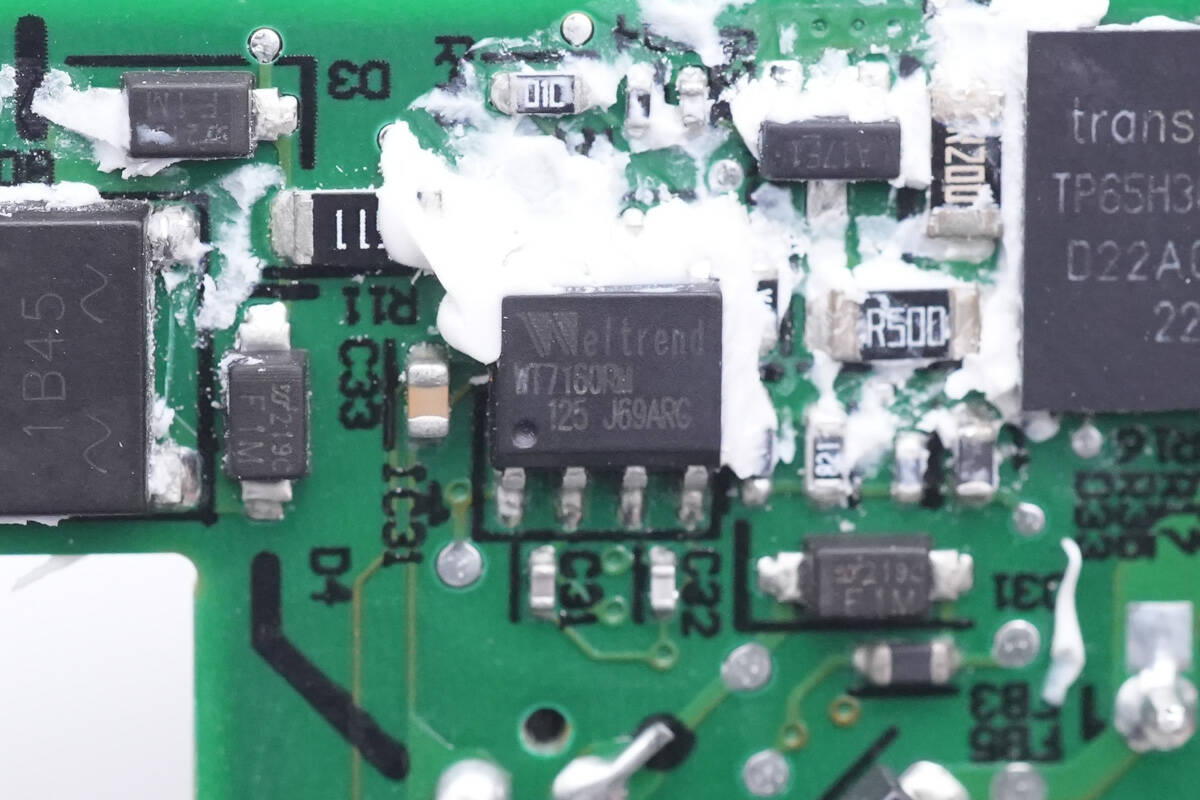
The primary controller is from Weltrend WT7160, which is a multi-mode Flyback controller. It integrates X-capacitor discharge and high-voltage startup features. And it can support a wide range of output voltage, external thermistor for overheating protection, multiple protection functions, and it adopts SOP8 package.
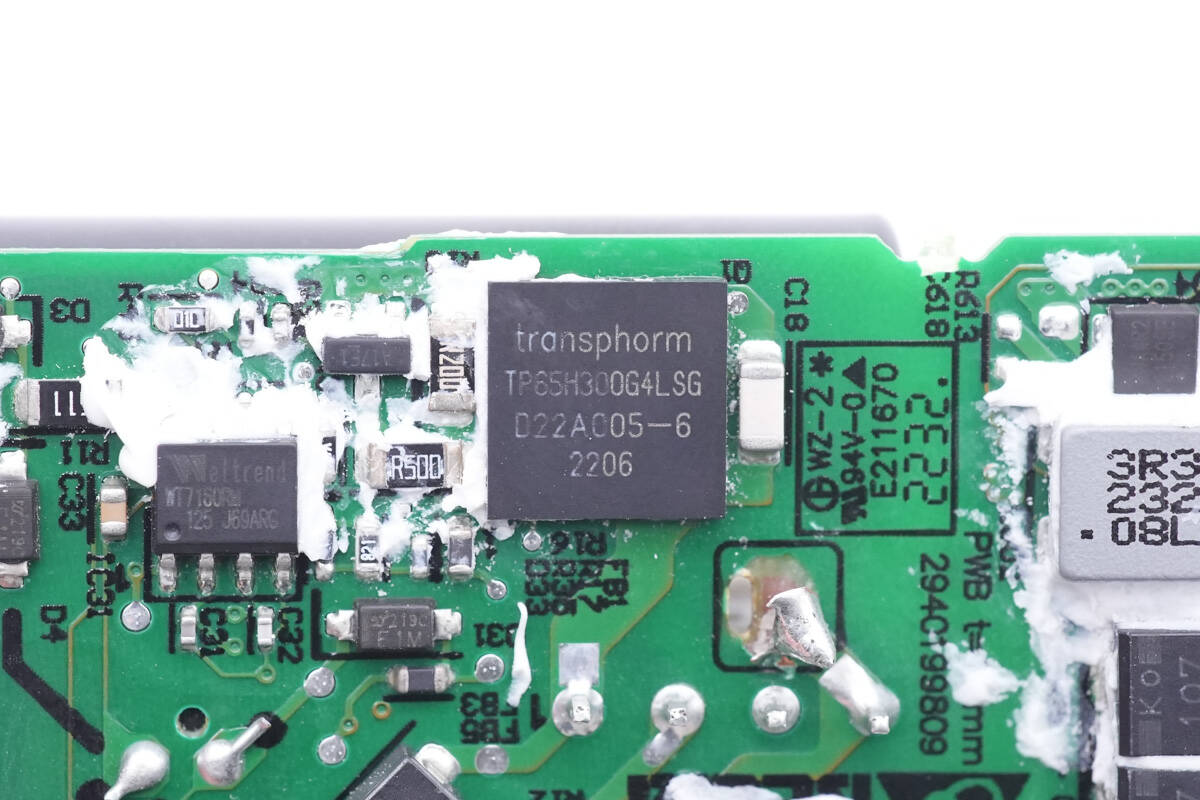
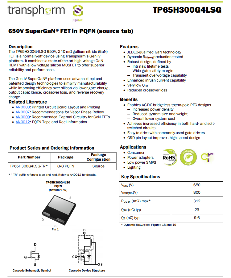
The GaN FET is from Transphorm TP65H300G4LSG, and adopts DFN8*8 package.
It has an extremely low reverse recovery charge and can reduce crossover loss. Compared with traditional silicon components, it can provide better energy efficiency, switching frequency and power density, less system size, weight and lower system cost. And it's suitable for fast-charging sources and LED lighting, etc. 650V 240mΩ.
ChargerLAB learned that Transphorm has also launched four SMD GaN components, which adopt TOLL 10x12 package for harsh environments. Dozens of products such as ASUS ROG 1600W Titanium Power Supply, Romoss 65W PD GaN Charger, HELPERS LAB 65W GaN Charger, etc, have also adopted its products. Customers have recognized the performance and quality of those products.
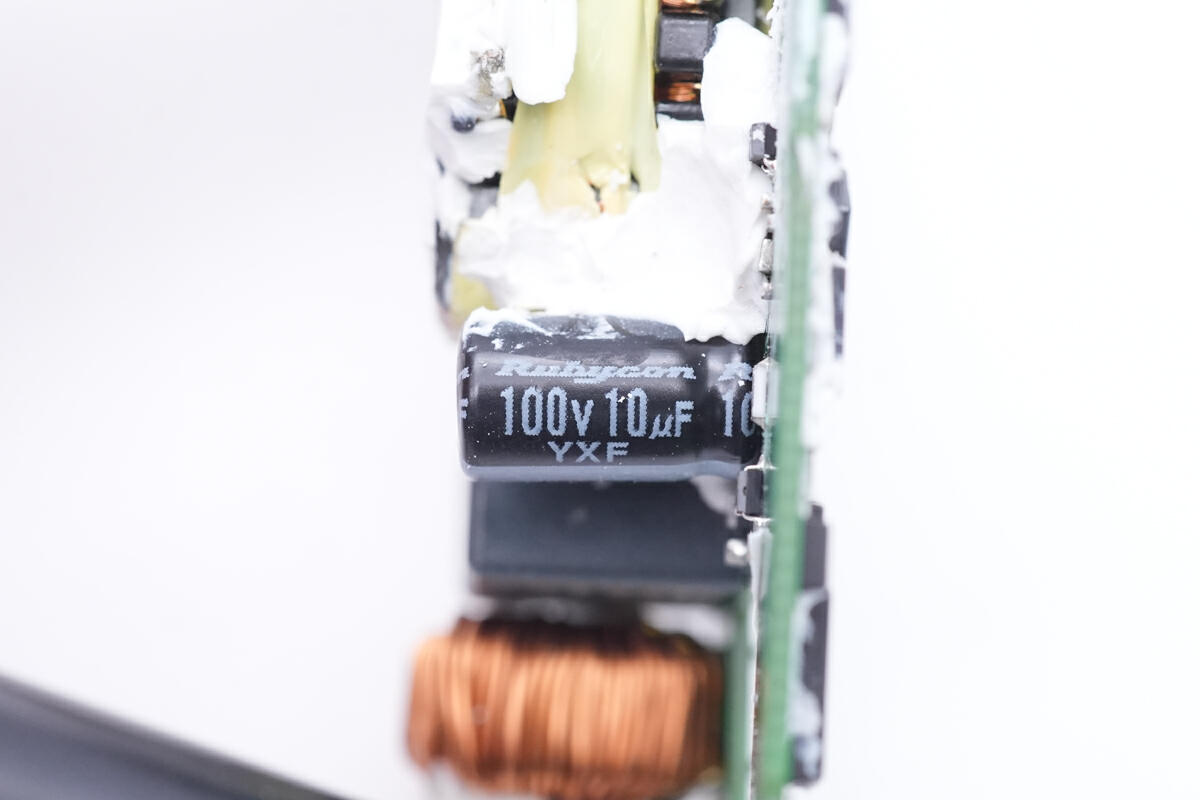
The electrolytic capacitor that powers the primary controller is from Rubycon. 100V 10μF.
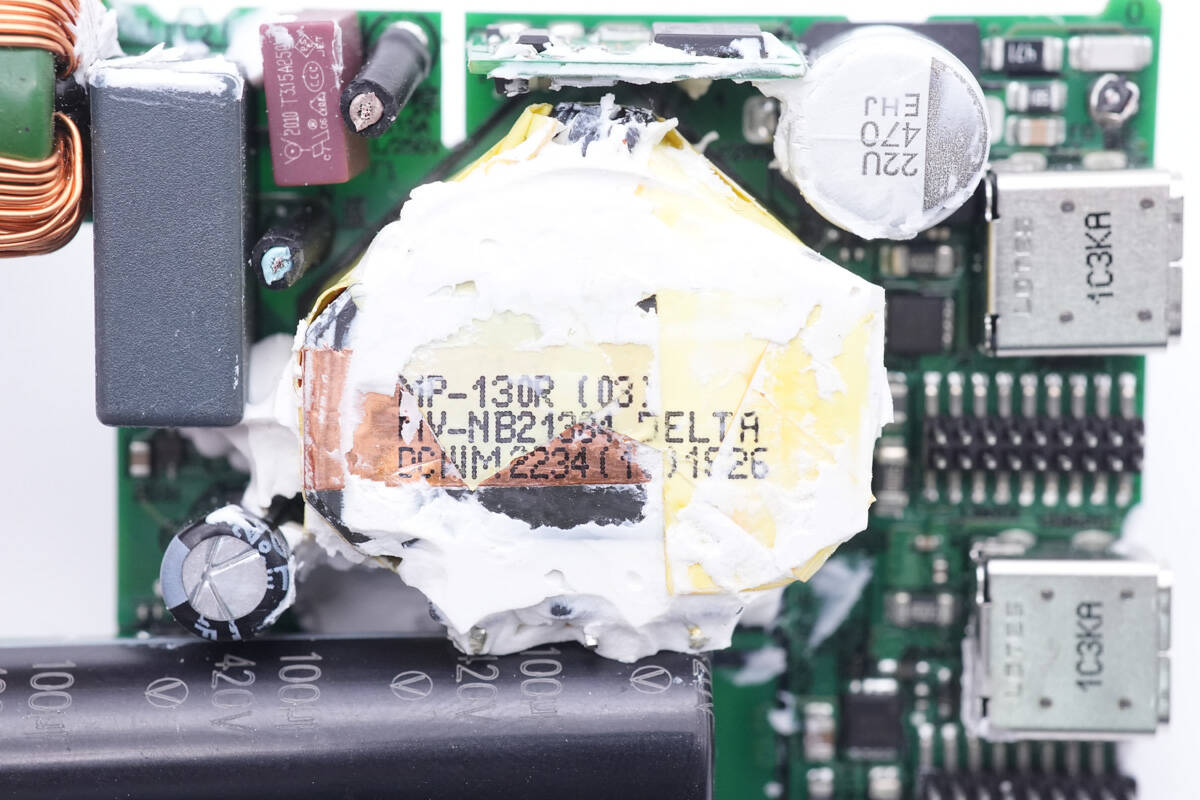
The transformer is from Delta, and the magnetic core is shielded with copper foil.
Close-up of two SMD Y capacitors connected in series.
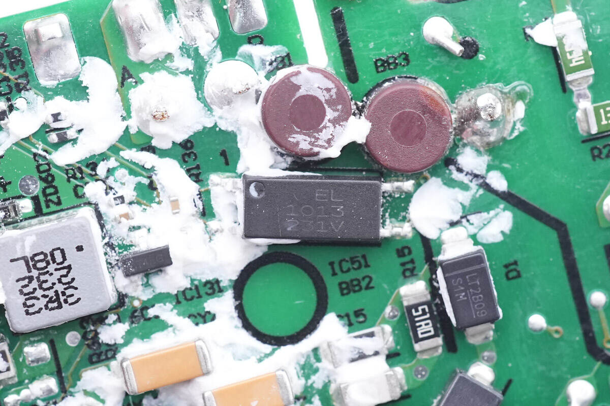
This EL1013 optocoupler is used for output voltage feedback.
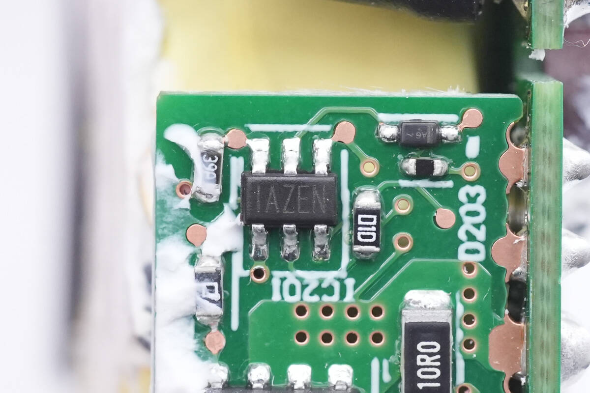
The synchronous rectifier controller marked with AZE is from MP, the model is MP6908, and it's a fast turn-off controller. And it supports DCM, CCM and QR operation modes, high-side and low-side rectifications and works with standard and logic level synchronous rectifier MOSFETs.
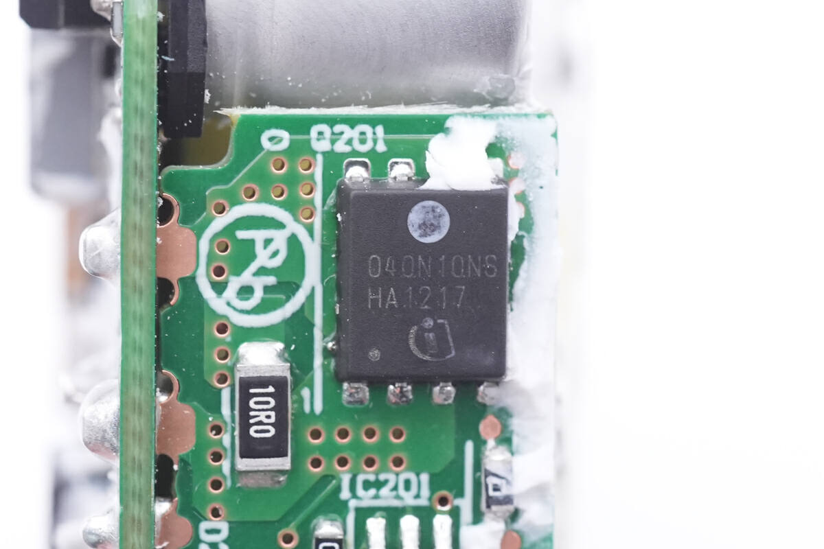
This synchronous rectifier is from Infineon, the model is BSC040N10NS5. 100V 4mΩ.
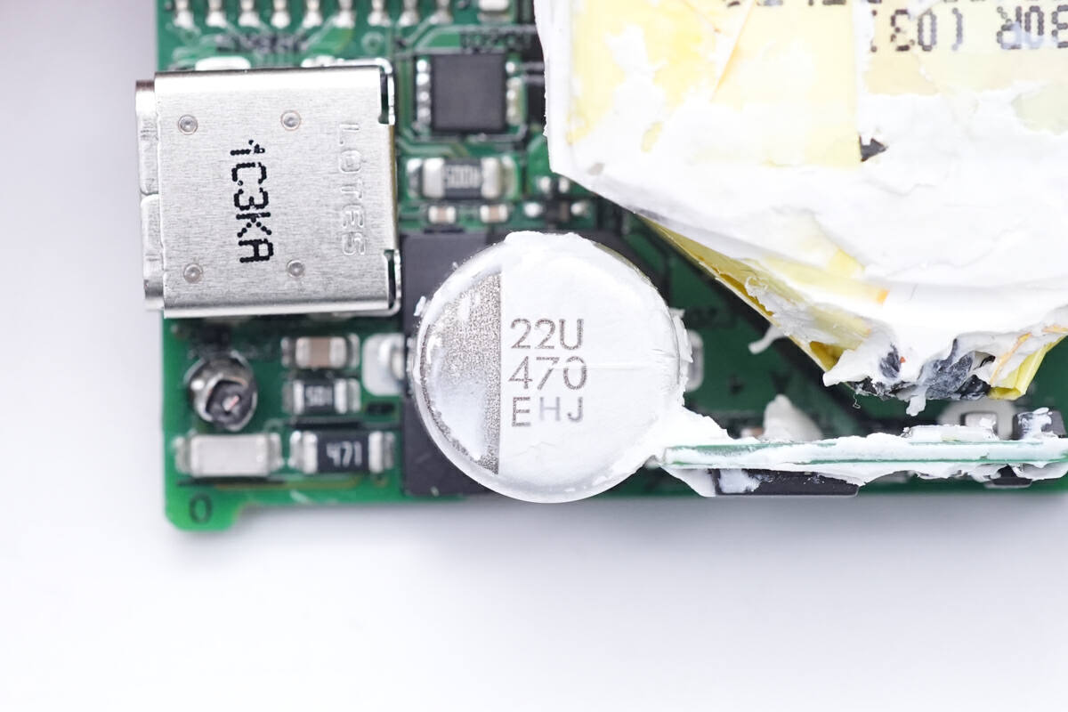
And this capacitor is used for output filtering. 25V 470μF.
The output protocol chip is soldered on this small PCB.
And it's connected to the main PCB through two connectors.
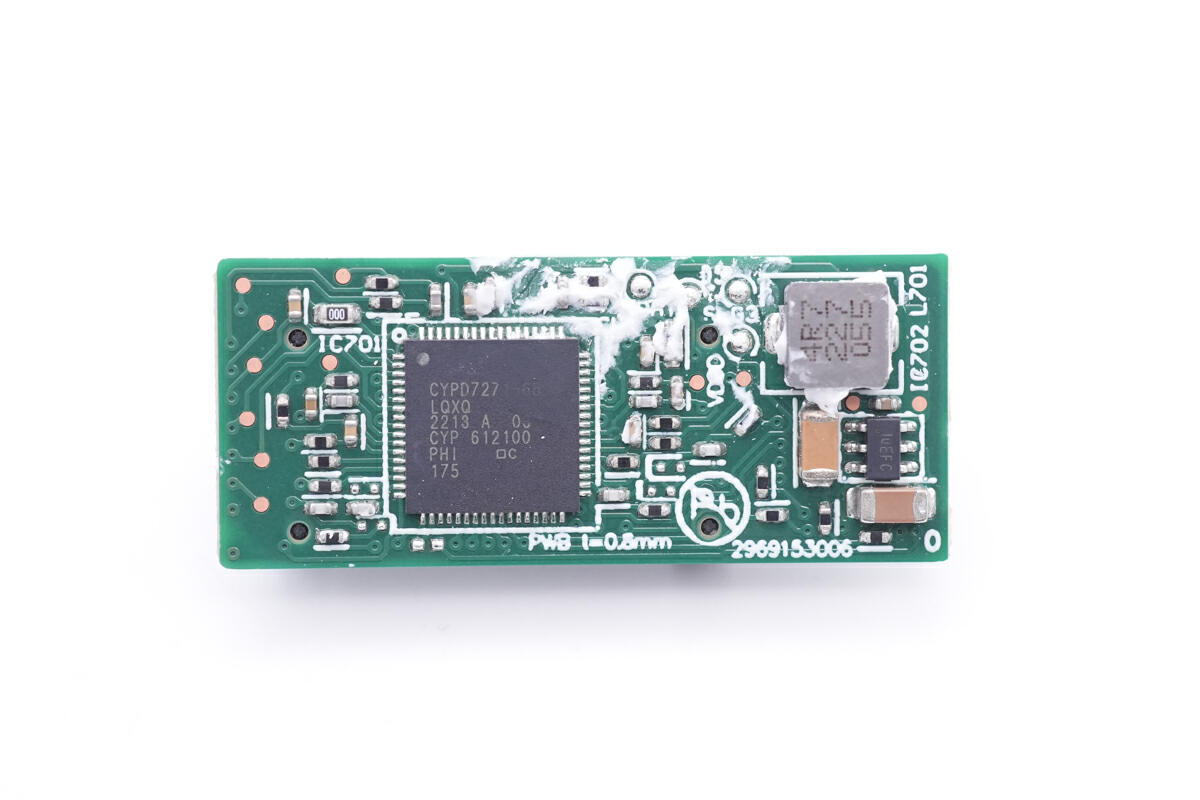
The output protocol chip and a buck circuit are soldered on the front of the small PCB.
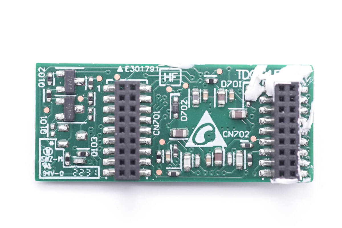
And two pin sockets are on the back.
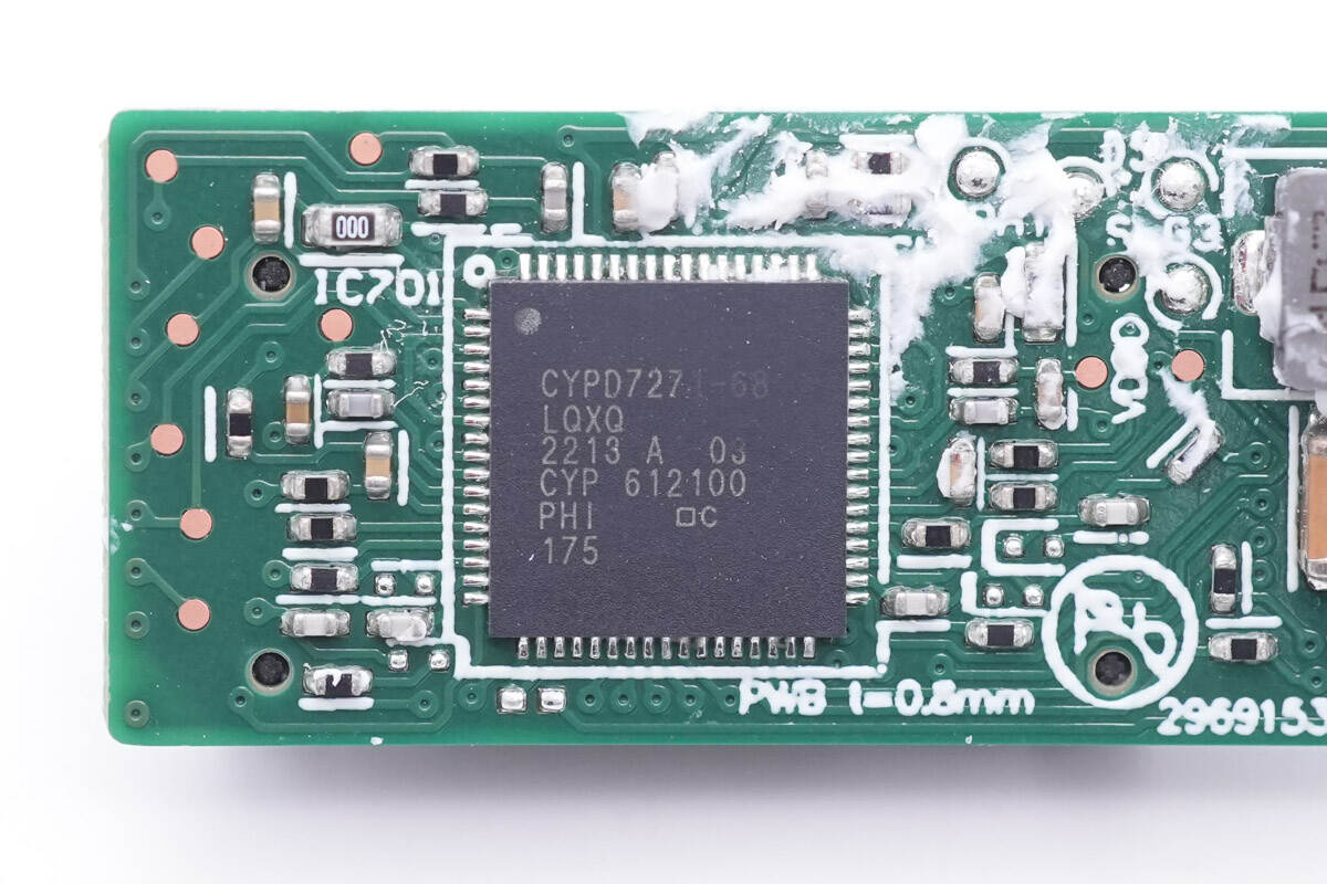
The protocol chip is from Infineon CCG7DC series, model is CYPD7271. It's a highly integrated USB Type-C power delivery (PD) solution with integrated buck-boost controllers for multi-port consumer charging applications. And it also integrated NMOS drivers to control VBUS MOSFET and hardware-controlled protection features. It supports a wide input voltage range from 4V to 24V and programmable switching frequency.
The chip integrates a built-in 32-bit M0 core processor, 128KB Flash, 16KB RAM and 32KB ROM, and it also includes analog and digital peripherals. It can support system function customization, such as dynamic load sharing.
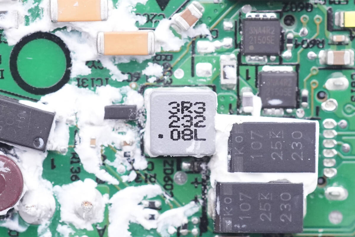
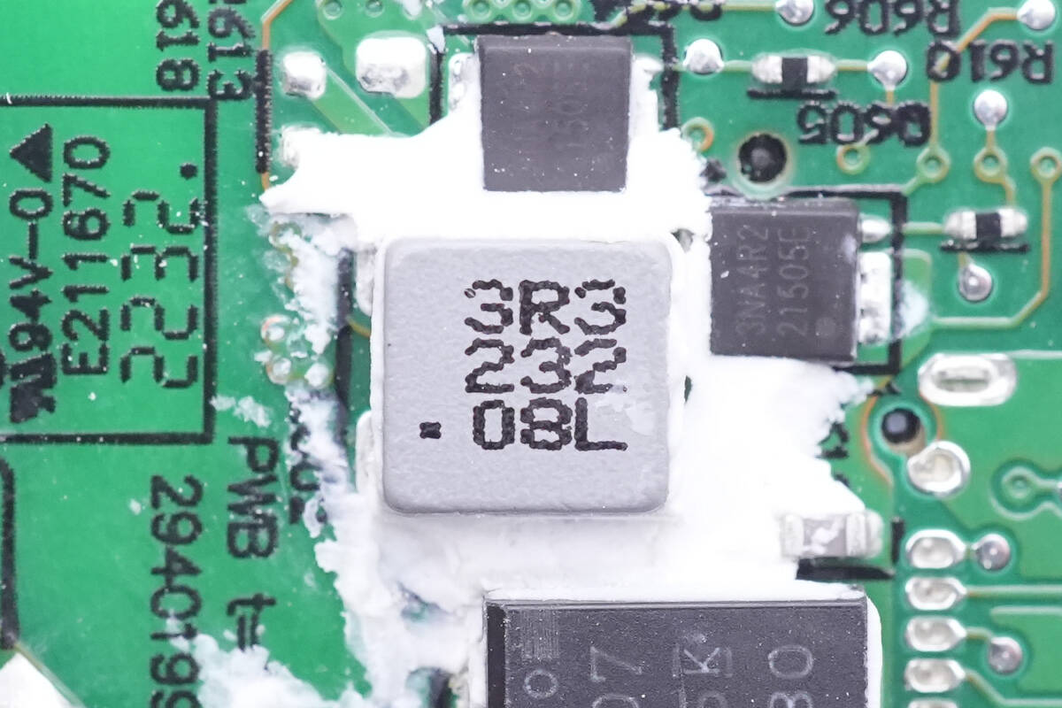
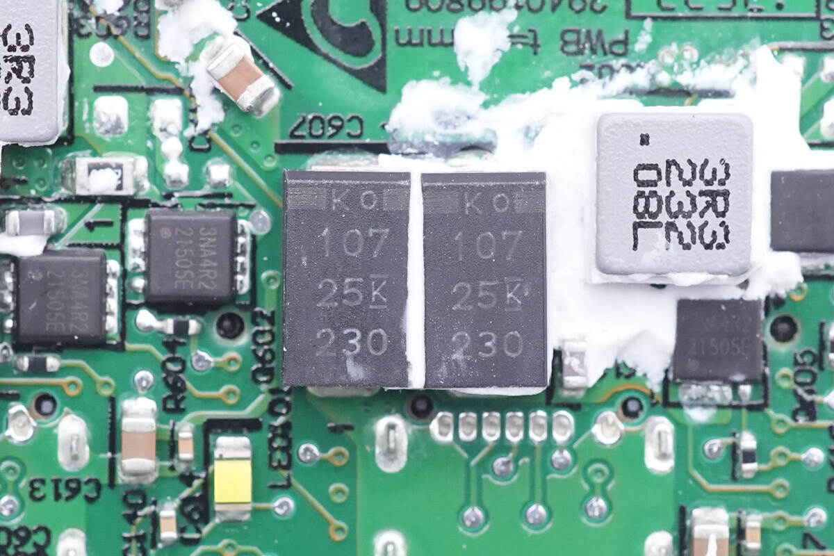
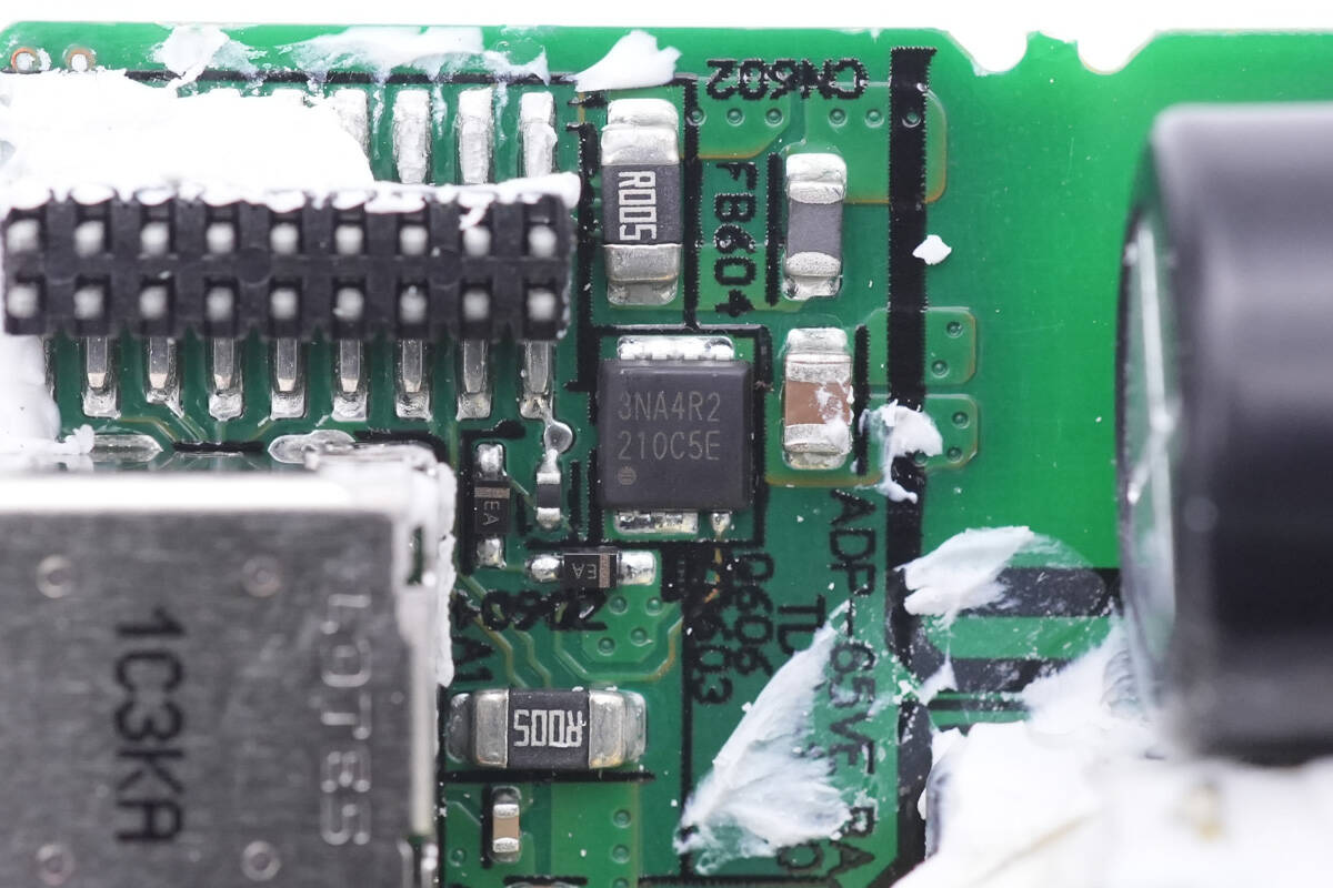
This is a 3.3µH alloy inductor for the buck output.
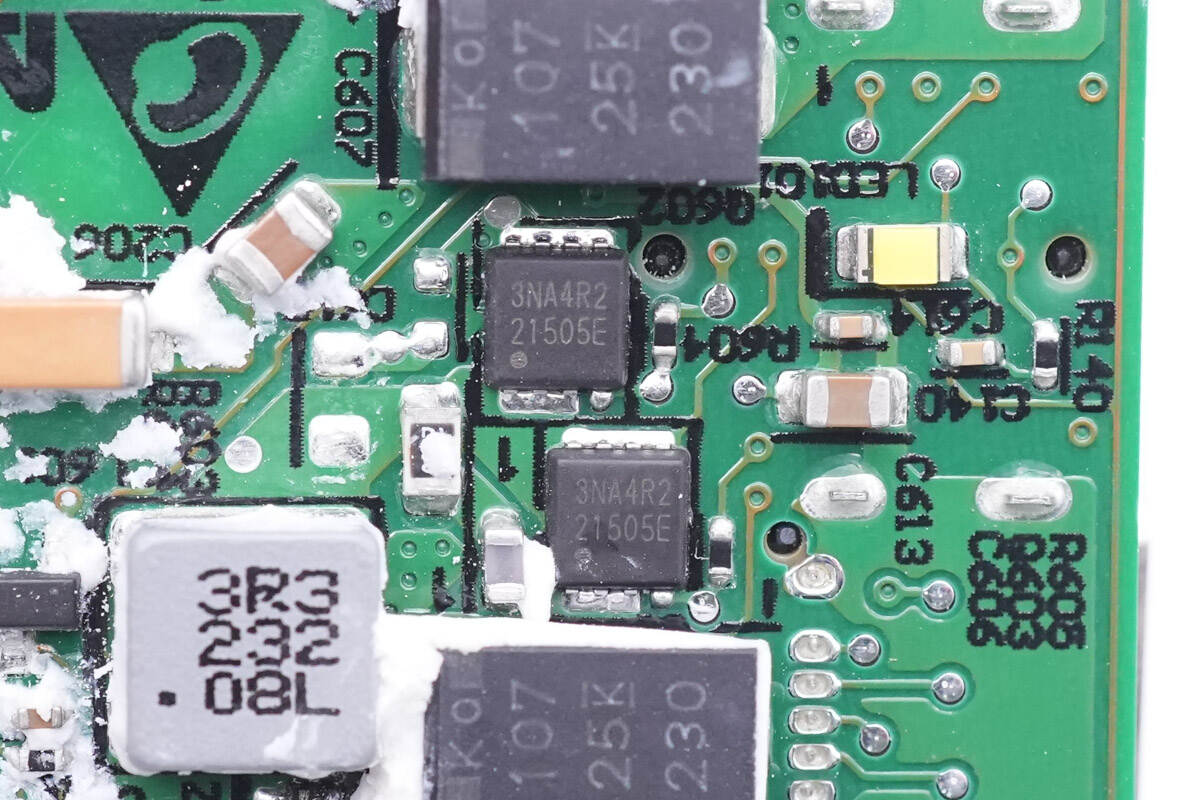
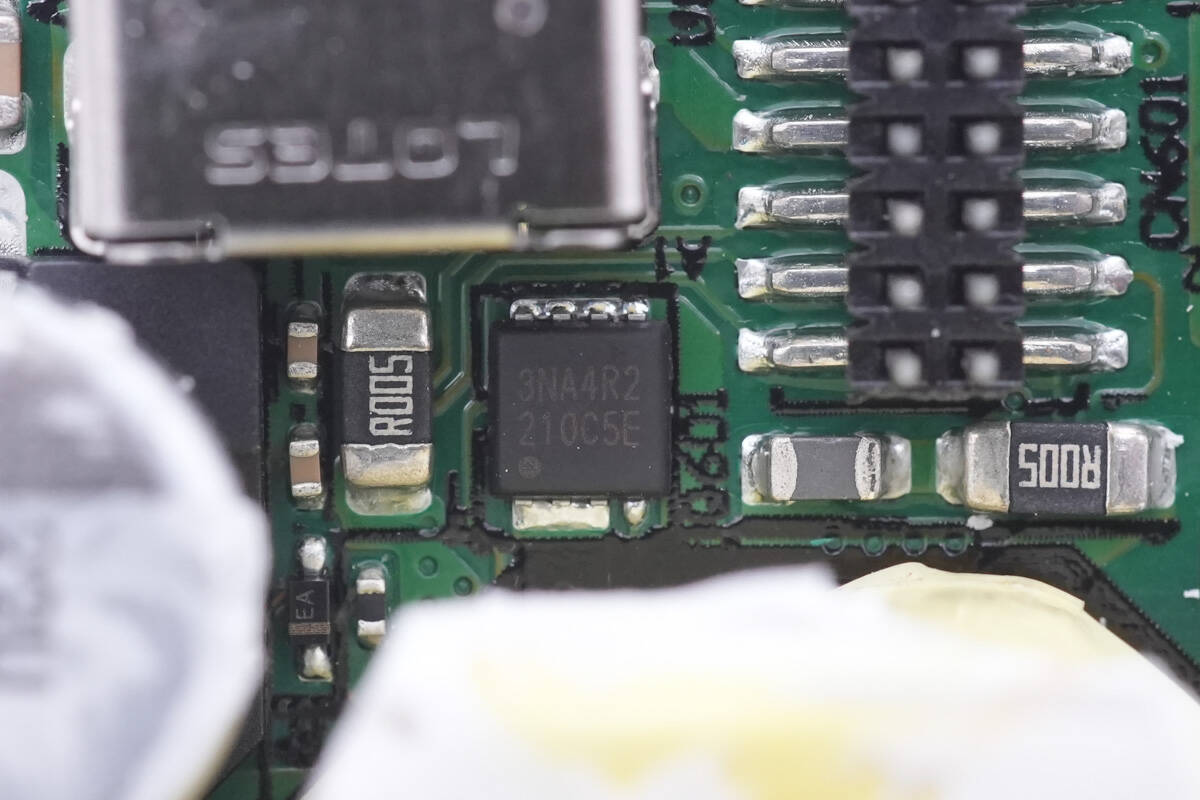
These two synchronous buck MOSFETs are from APEC, the model AP3NA4R2YT, and adopt PMPAK3*3 package. 30V 4.2mΩ.
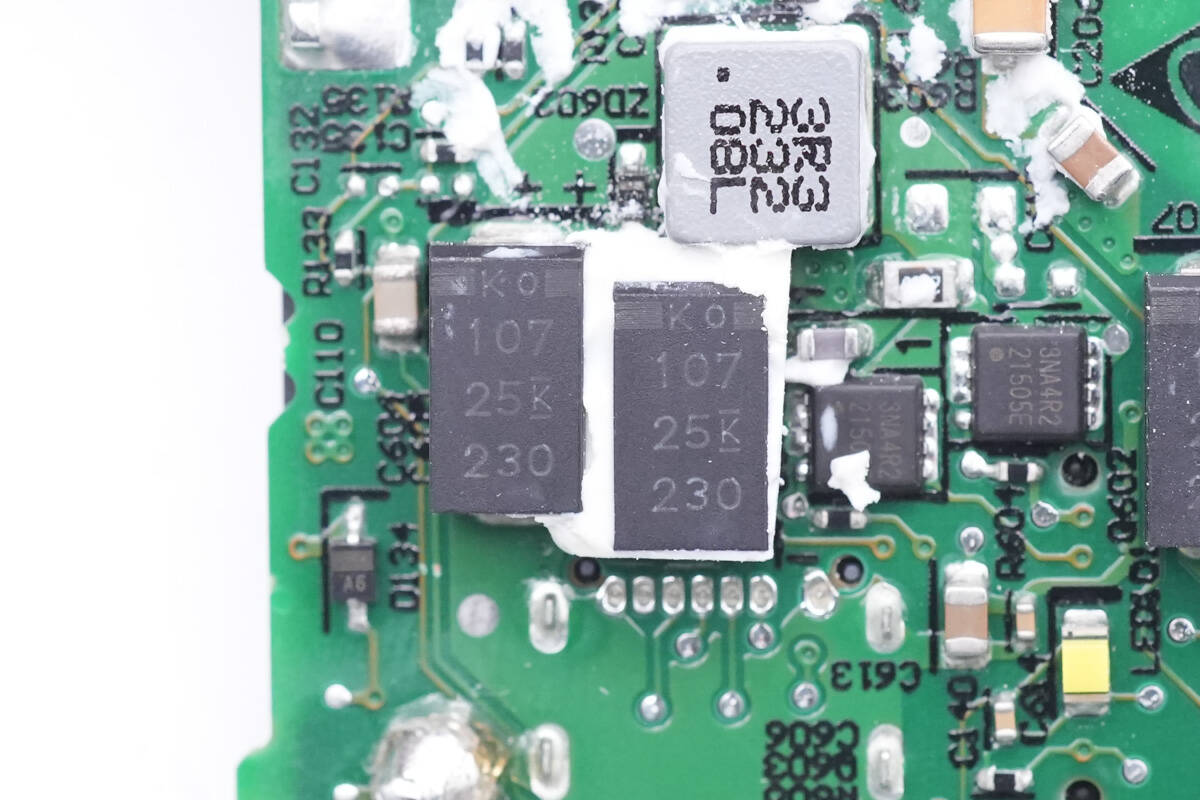
Those two capacitors for output filtering are from KEMET. 100μF 25V.
This is the buck inductor for the output of another circuit.
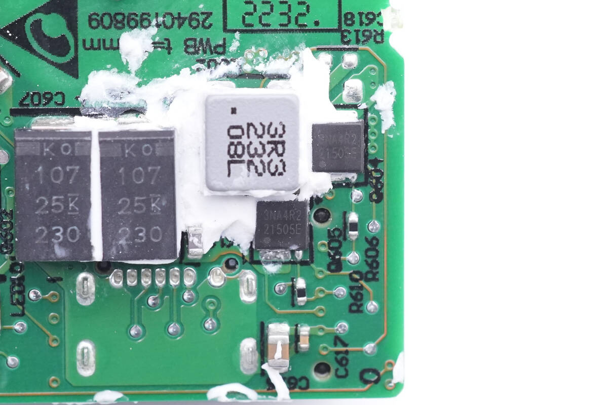
On the right side of that inductor is the buck MOSFET.
Those two capacitors for output filtering are also from KEMET. 100μF 25V.
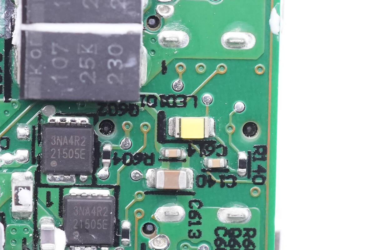
Close-up of the indicator light.
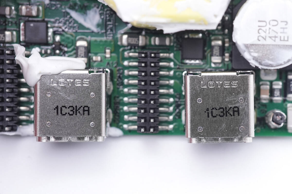
Below the small PCB are two USB-C sockets, which come from LOTES.
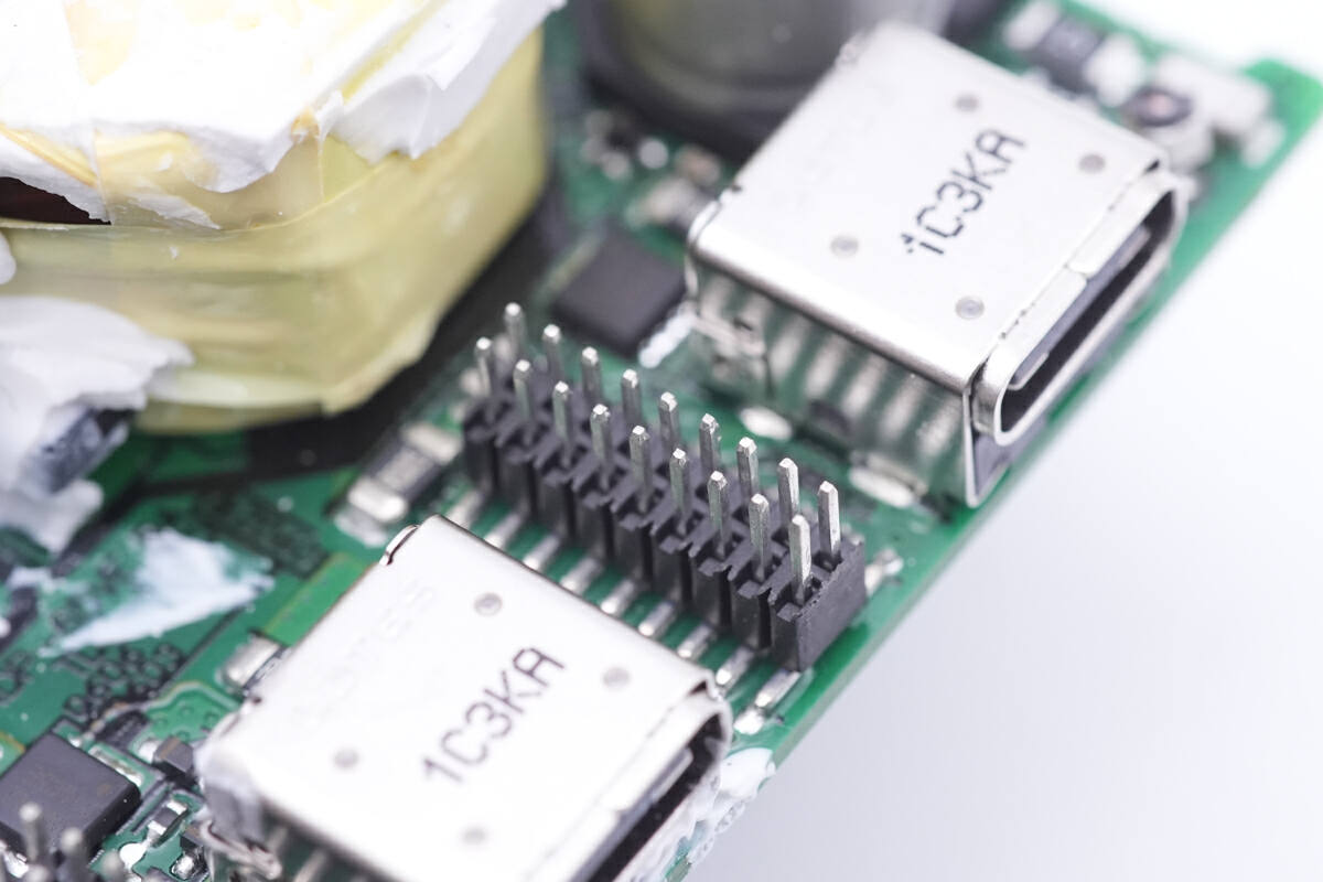
Close-up of the pins connected to that small PCB.
The model of the VBUS MOSFET is the same as the buck MOSFET.
Another VBUS MOSFET of the same model.
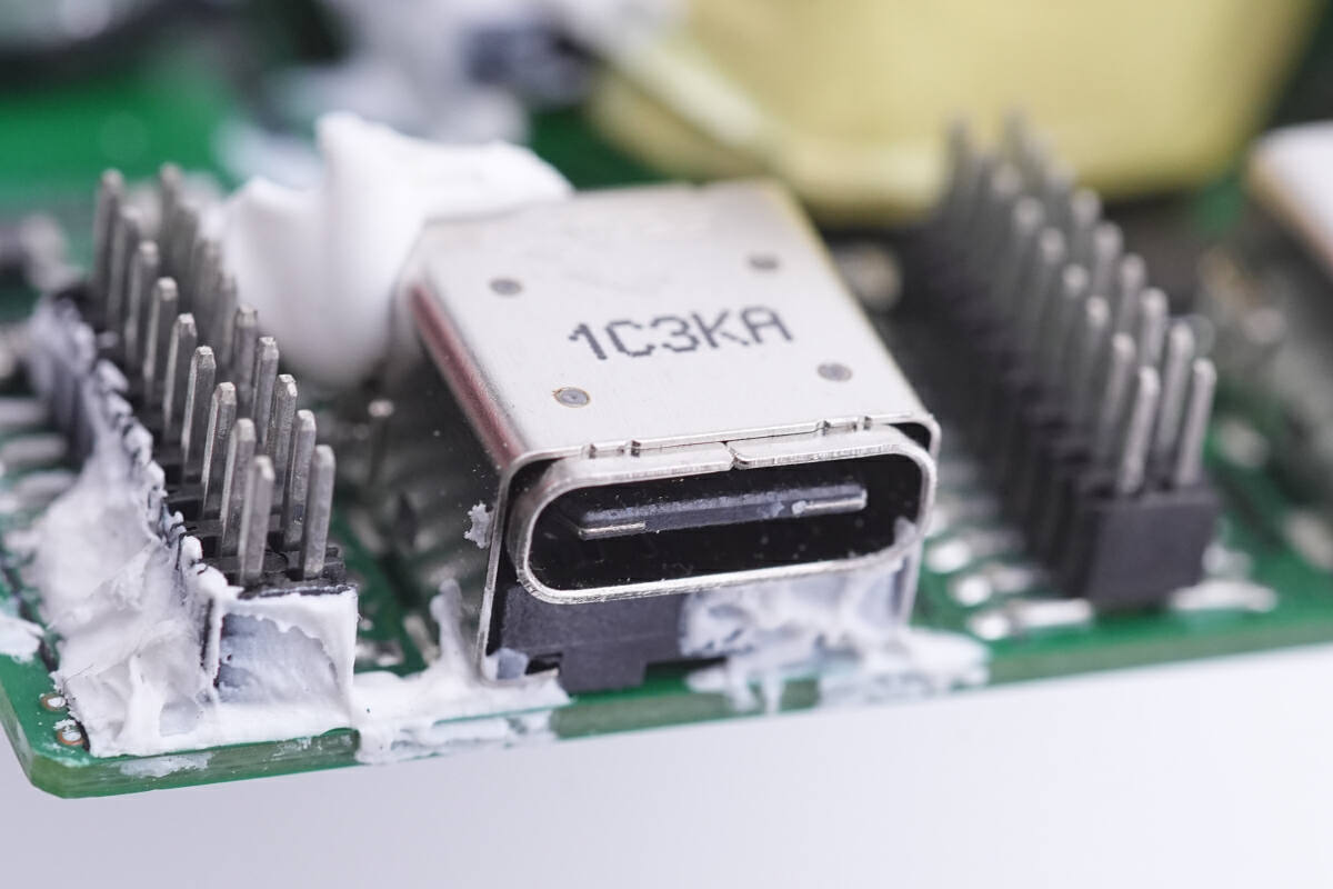
The USB-C socket is wrapped with a steel sleeve.
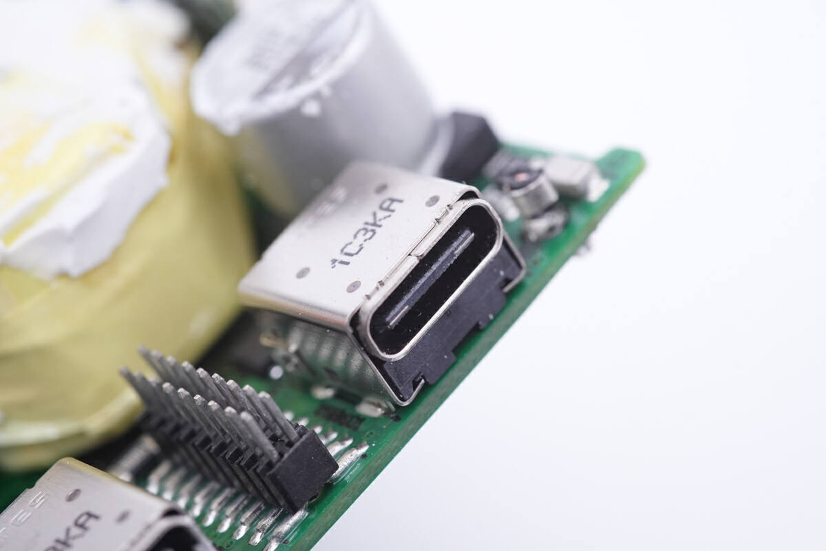
And the sheet is black.
That's all for the teardown.
Summary of ChargerLAB
This HP 65W dual USB-C GaN power adapter adopts a black matte design with two detachable cables. The grounding prong inside the input socket can protect the user from electric shock.
After taking it apart, we found the PCBA module is wrapped with copper sheet for better heat dissipation performance. It uses Transphorm GaN FET, and the primary controller is from Weltrend. The protocol chip is from Infineon CCG7DC series.
The GaN component can effectively increase the efficiency of the adapter and reduce heat generation during fast charging. Compared with 170 mΩ GaN of other companies, it adopts 240 mΩ GaN from Transphorm and still achieves high efficiency.