Introduction
Recently, ChargerLAB got a 45W power adapter from the well-known company Google. Compared with common chargers, Google's design is quite recognizable, with prongs on a disc base and a rounded body, and it uses GaN technology. It has a USB-C port and supports PD3.0 and PPS fast charging. Next, let's take it apart to see its internal components and structure.
Product Appearance
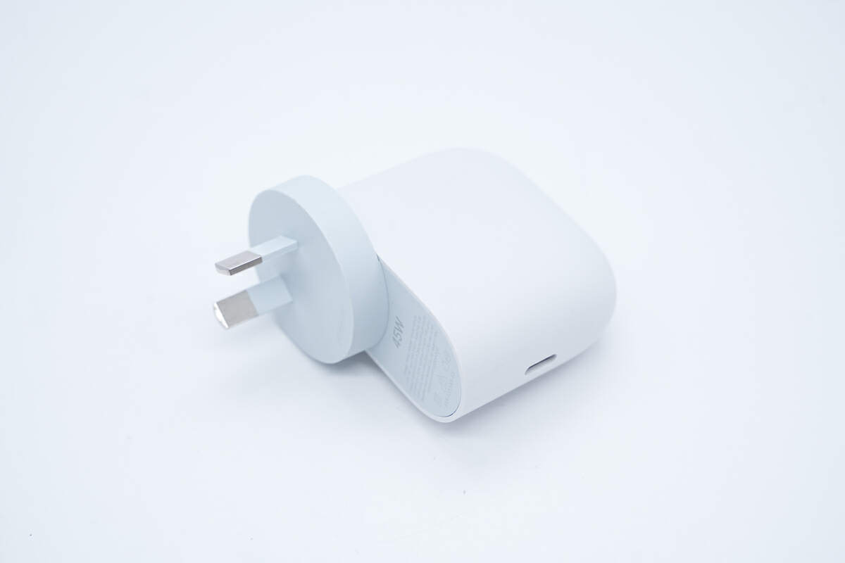
The Google 45W GaN Power Adapter's gray case is made of fire retardant PC. The surface of the case is matte, and the sides and edges are rounded.
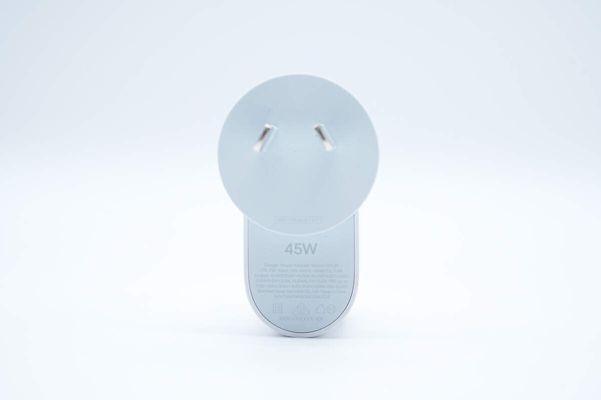
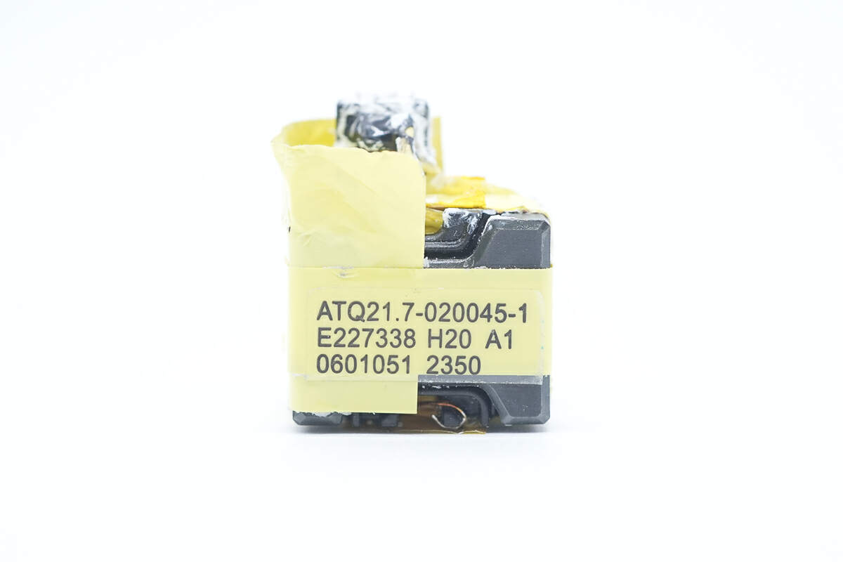
To improve stability, the prongs are on a disc base, and the specs info is printed under the disc.
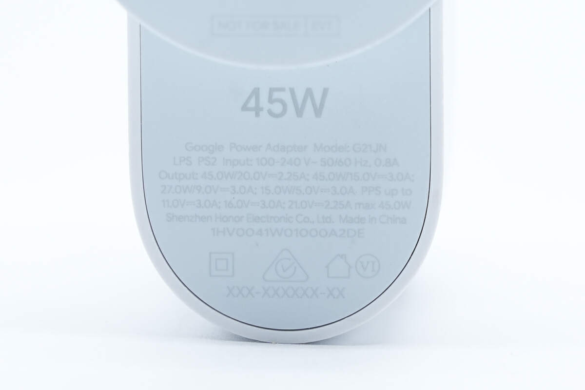
Model is G21JN. It can support input of 100-240V~50/60Hz 0.8A. The maximum output power is 45W. It has three sets of PPS, which are 5-11V3A, 5-16V3A, and 5-21V2.25A. It is certified for Level VI energy efficiency.
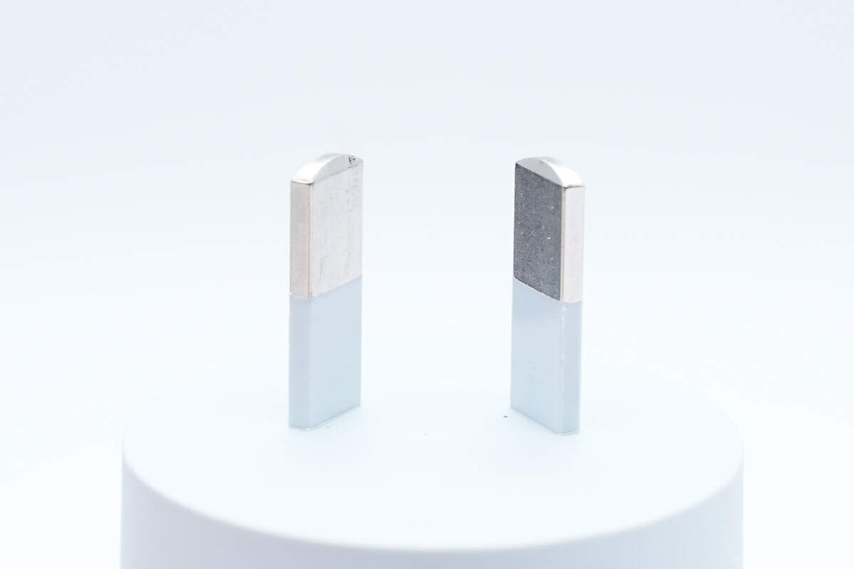
It adopts the Australian standard plug.
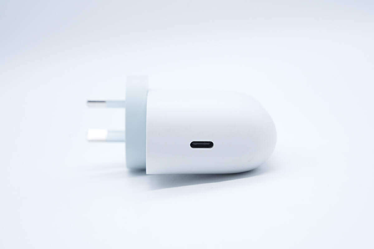
It only has a single USB-C port.
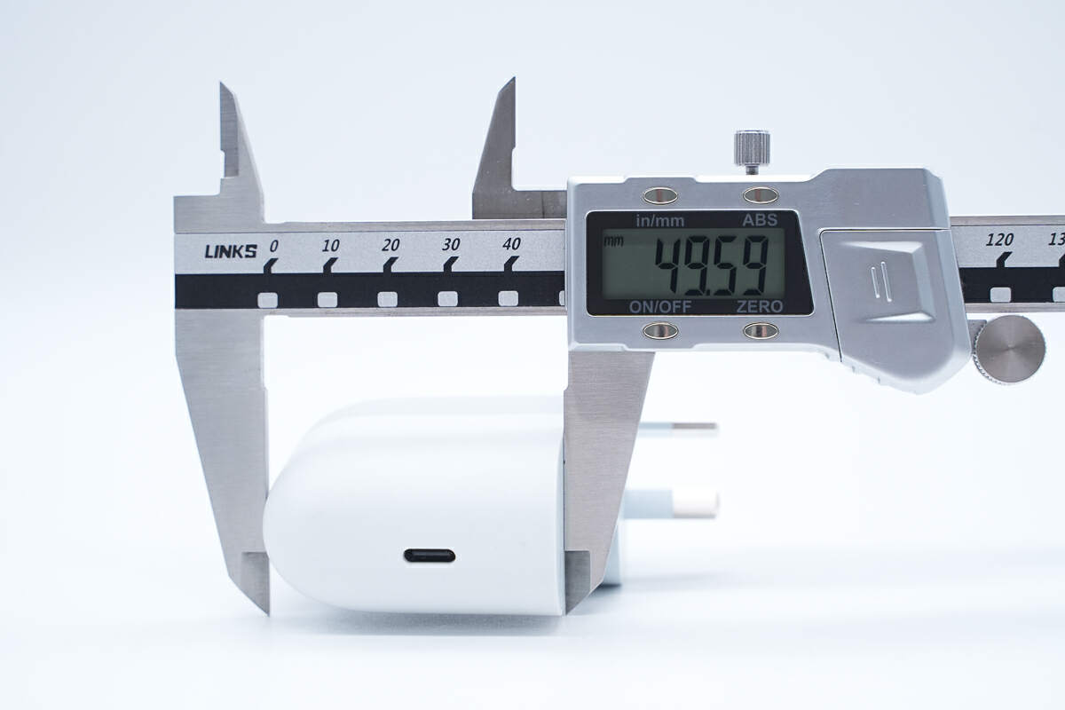
The length of it is about 49.6 mm (1.95 inches).
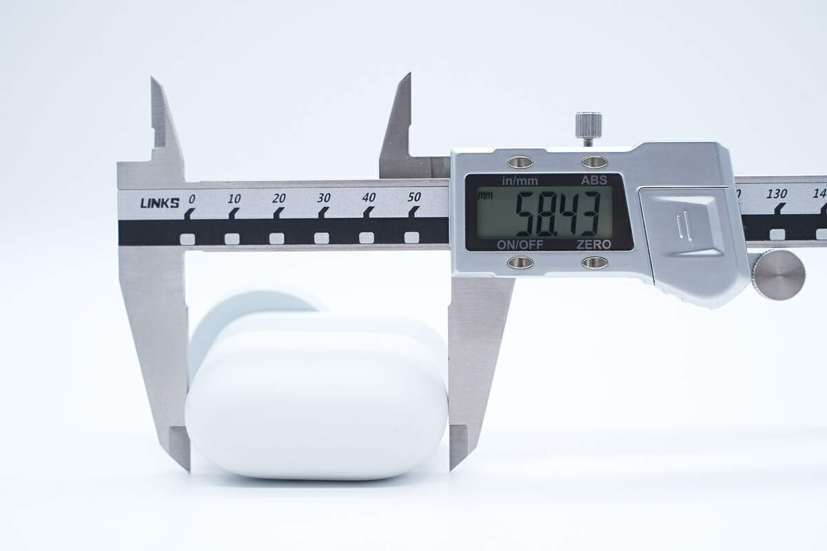
The width is about 58 mm (2.28 inches).
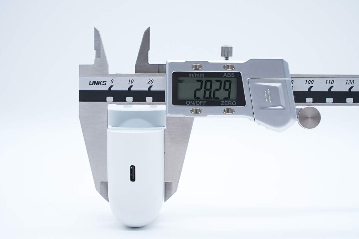
The thickness is about 28 mm (1.1 inches).
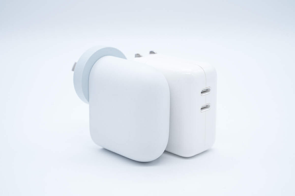
Compared with the Apple 35W charger, it is smaller.
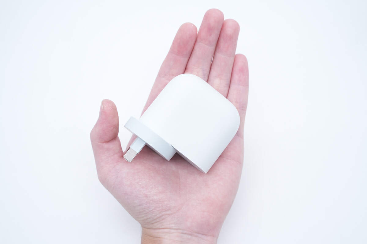
That's how big it is in the hand.
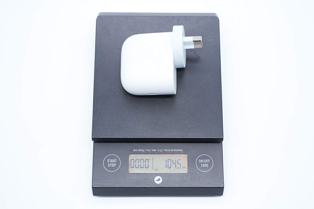
The weight is about 105 g (3.7 oz).
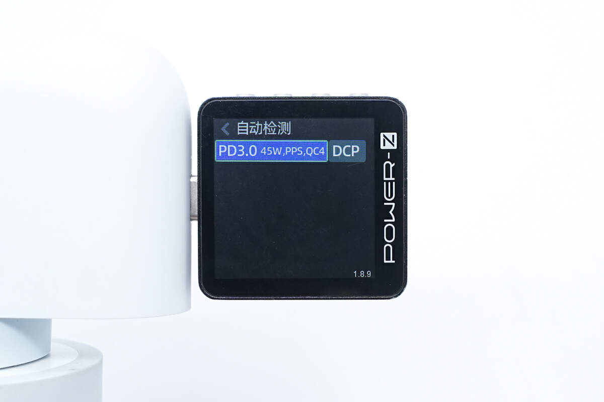
ChargerLAB POWER-Z KM003C shows the USB-C port can support PD3.0, PPS, QC4, and DCP charging protocols.
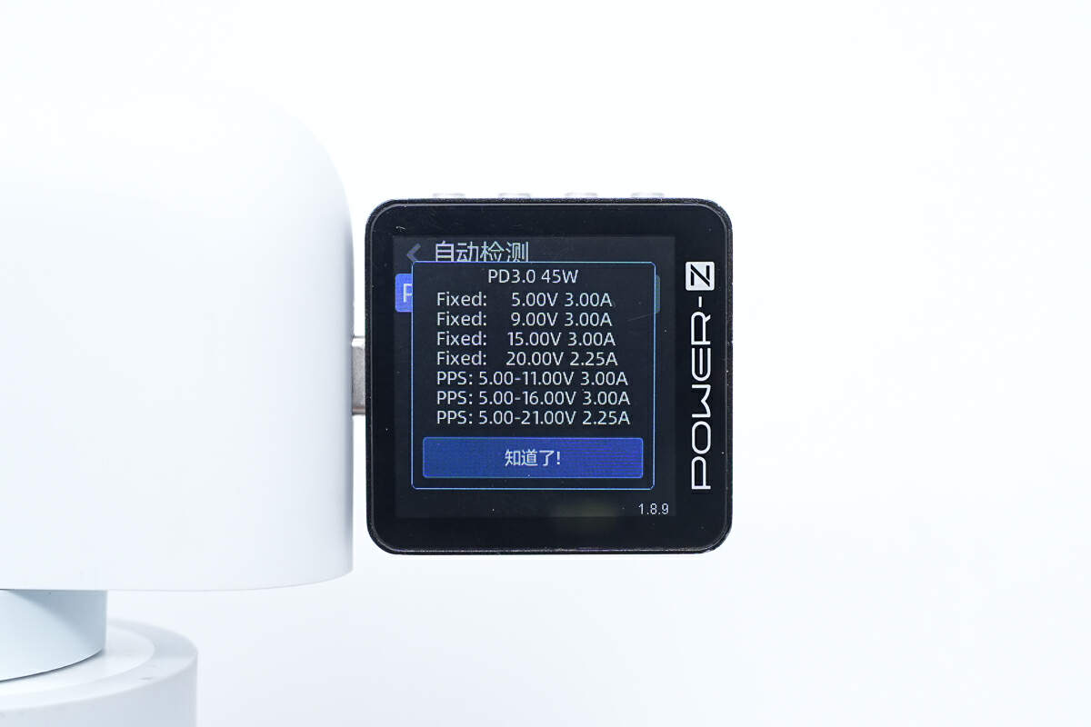
And it has four fixed PDOs of 5V3A, 9V3A, 15V3A, 20V2.25A, and three sets of PPS, which are 5-11V3A, 5-16V3A, and 5-21V2.25A.
Teardown
Next, let's start to take it apart and take a look at the internal components.
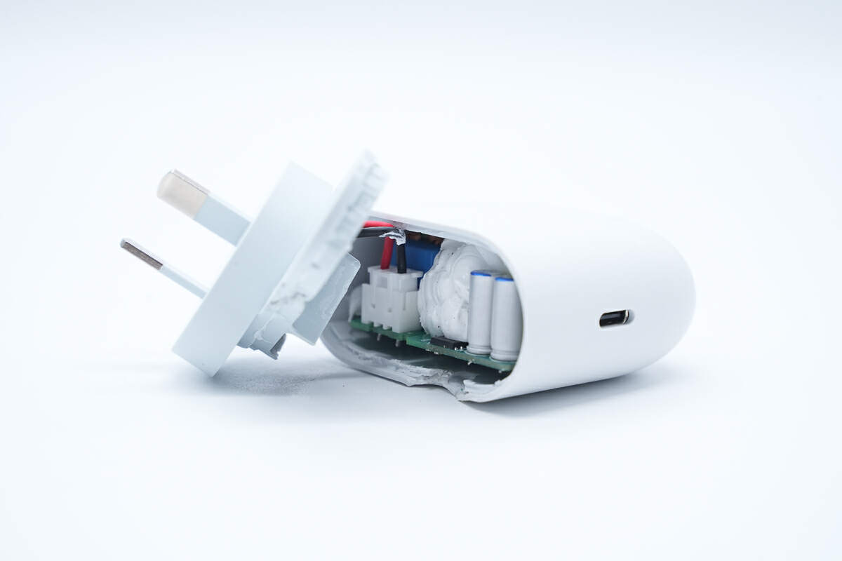
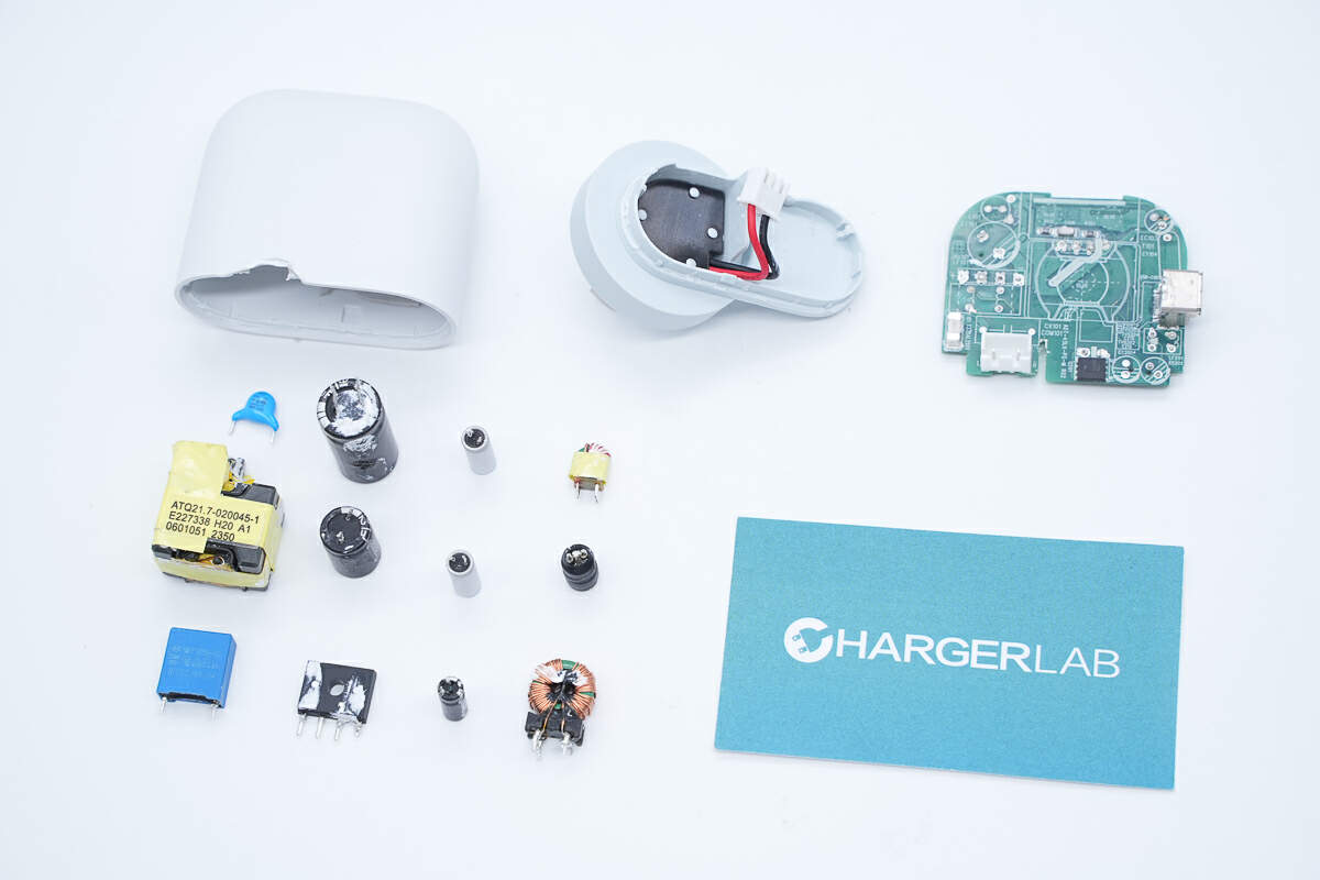
First, pry off the bottom case along the gap, which uses an ultrasonic welding process. The plug is connected to the PCBA module through wires.
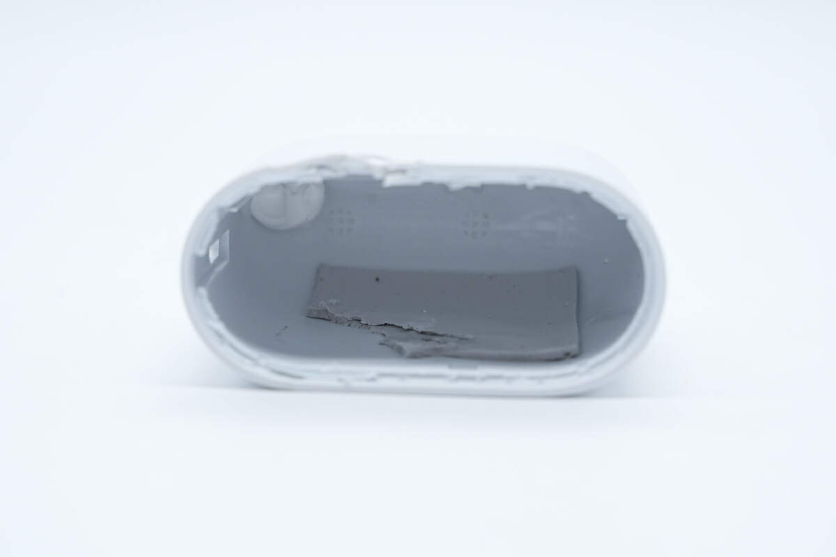
Take out the PCBA module, and there is a thermal pad inside the case to help dissipate heat.
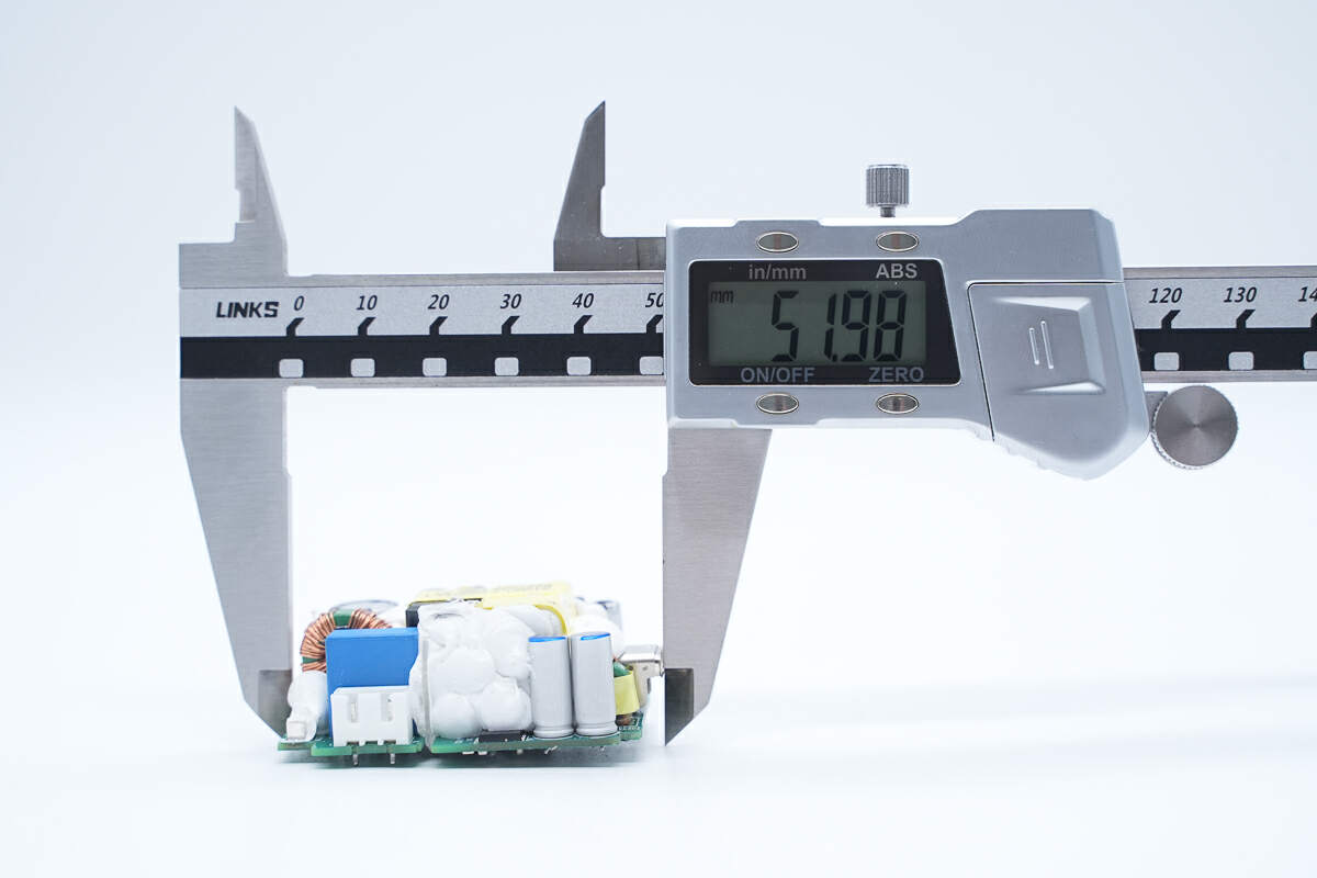
The length of the PCBA module is about 52 mm (2.047 inches).
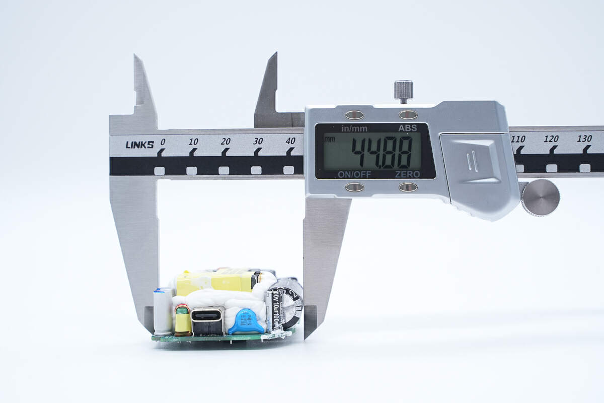
The width is about 44.9 mm (1.77 inches).
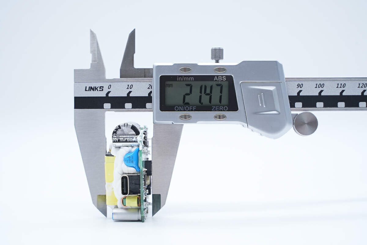
The thickness is about 21.5 mm (0.85 inches).
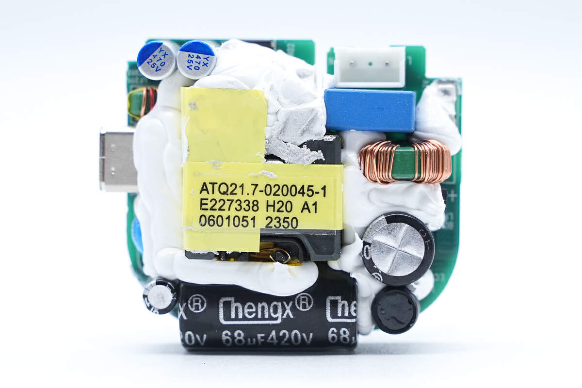
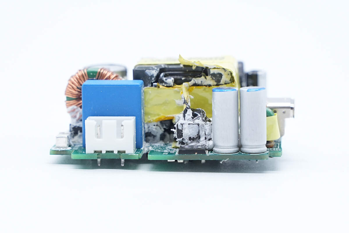
The gaps between components on the front side of the PCBA module are reinforced by filling with potting compound.
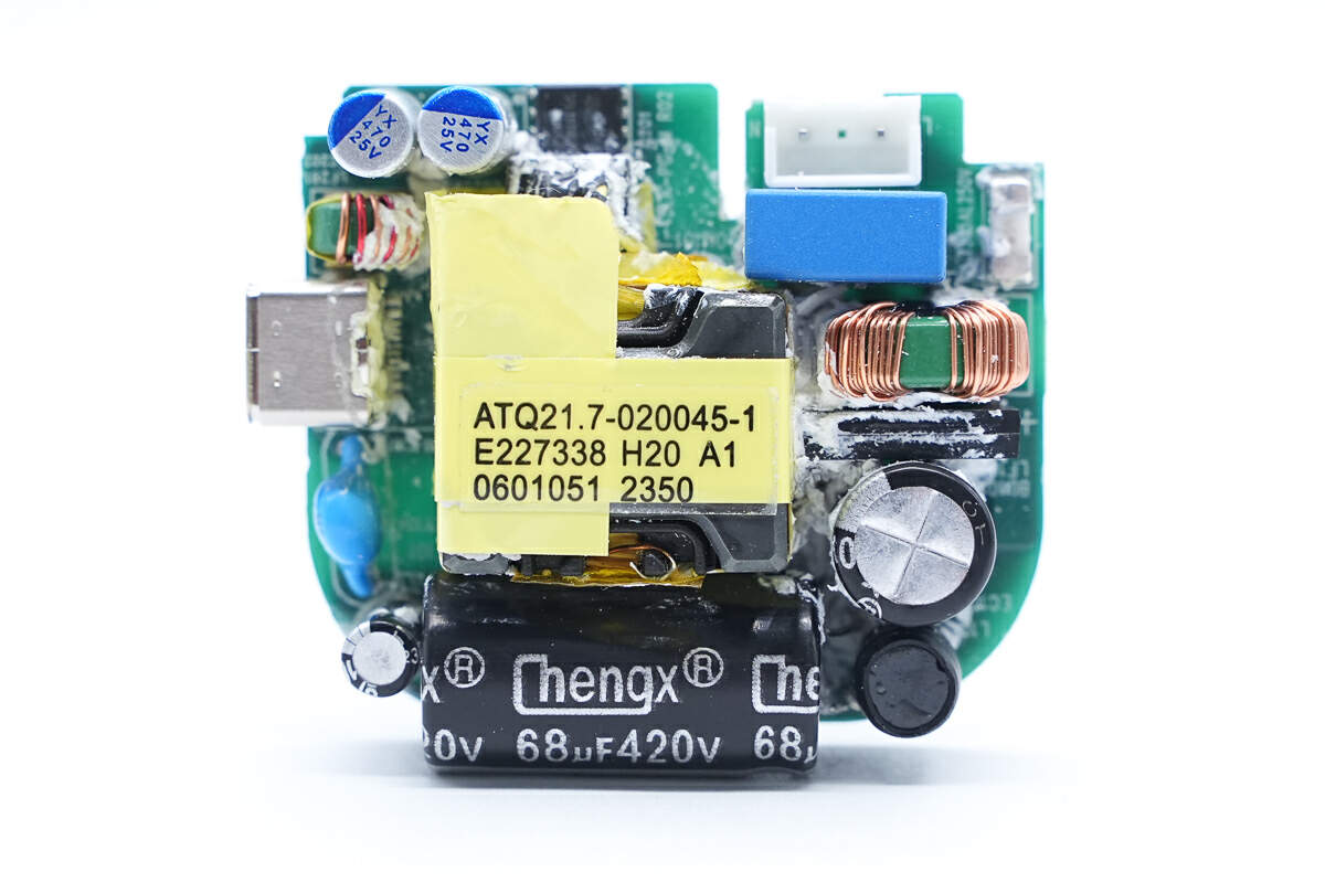
Clean up the potting compound.
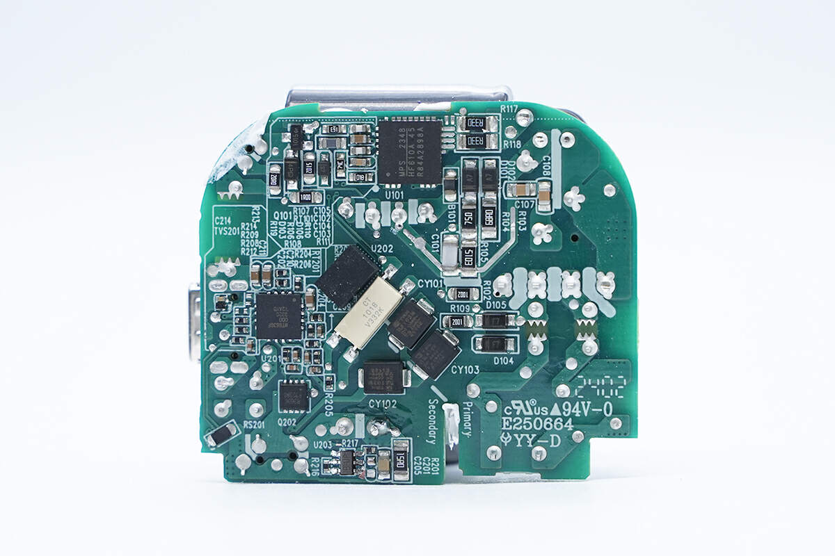
The master control chip, optocoupler, SMD Y capacitor, protocol chip, and output VBUS MOSFET are on the back of the PCBA module.
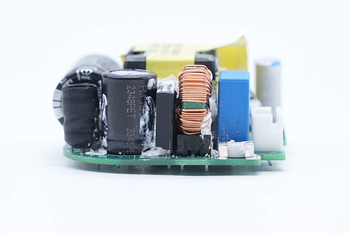
The input end is equipped with an SMD fuse, safety X2 capacitor, common mode choke, bridge rectifier, electrolytic capacitor for input filtering, and an I-shaped inductor.
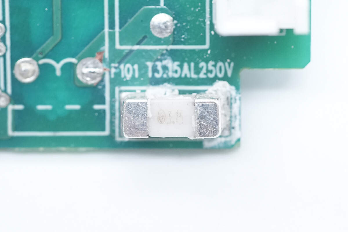
There is the SMD fuse. 3.15A.
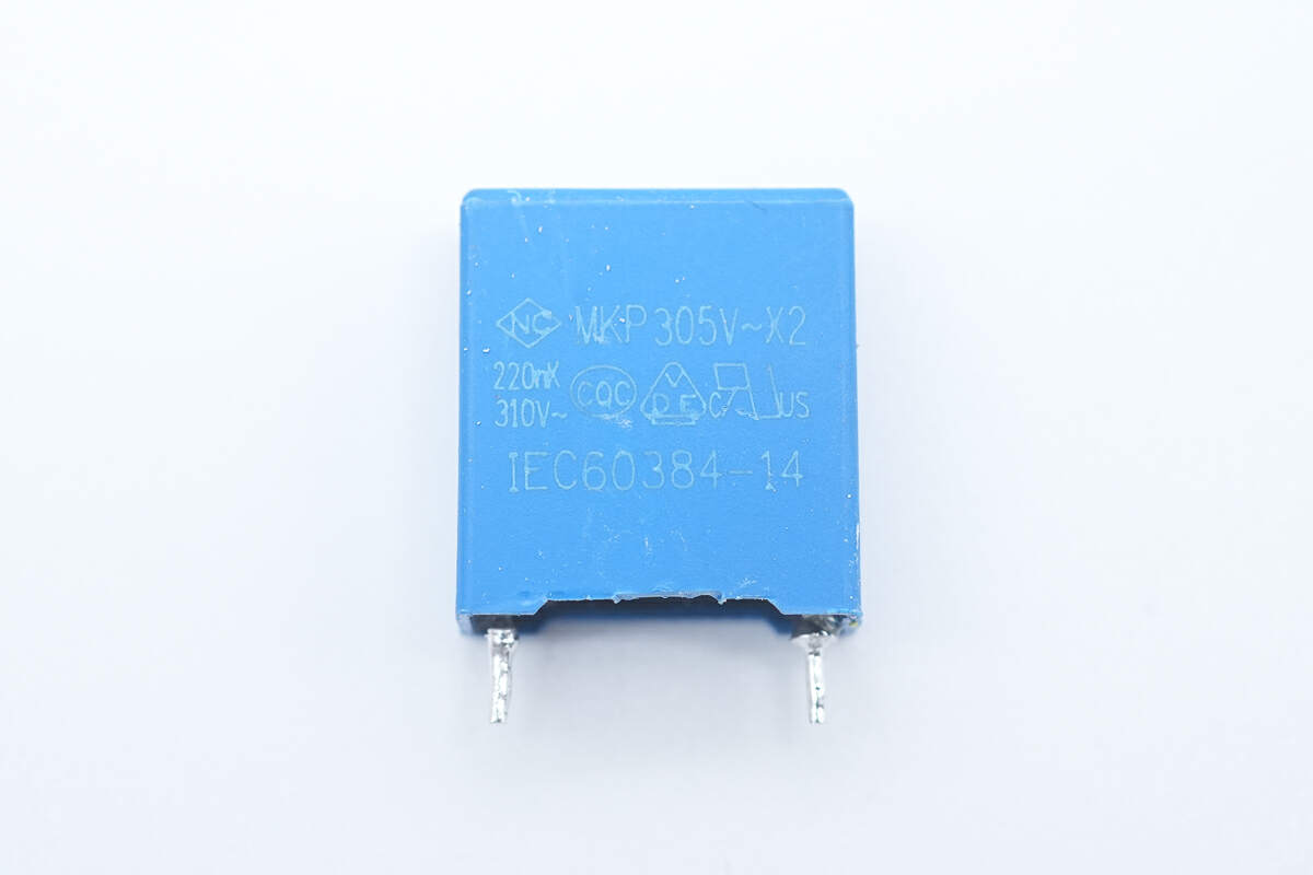
There is the safety X2 capacitor.
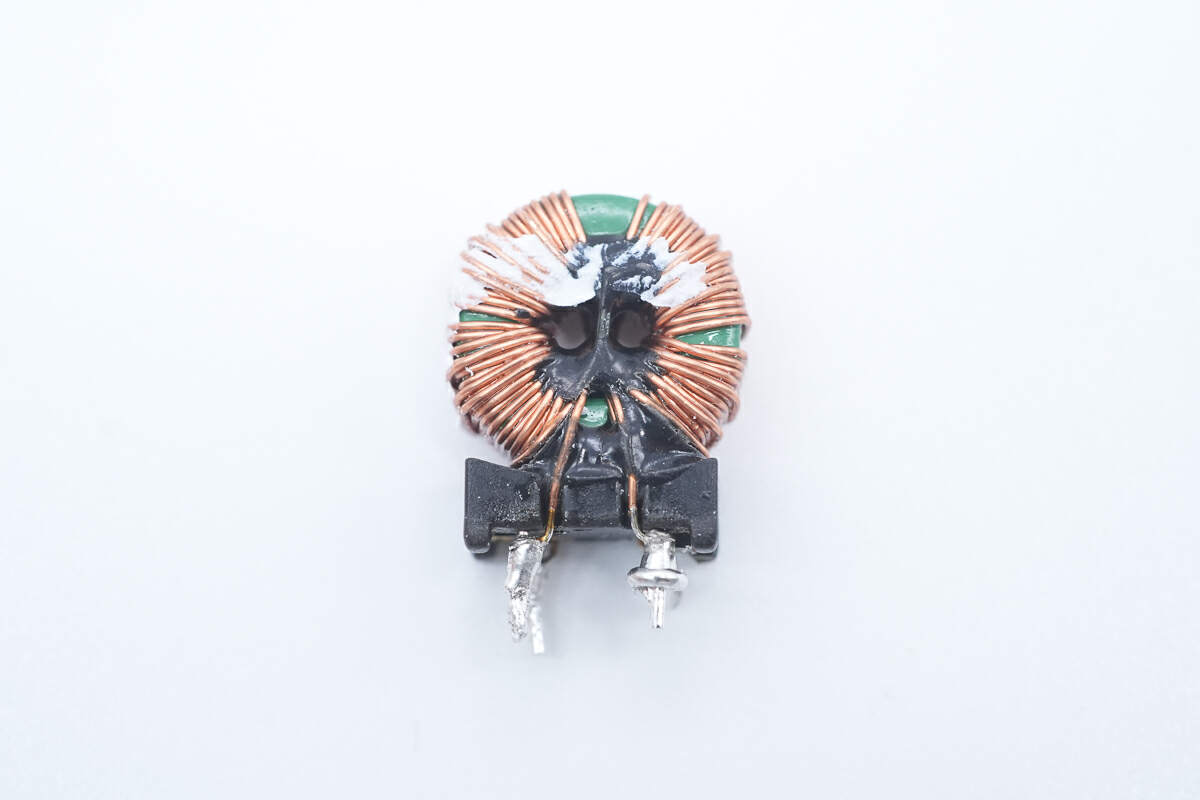
This is the common mode choke used to filter out EMI interference.
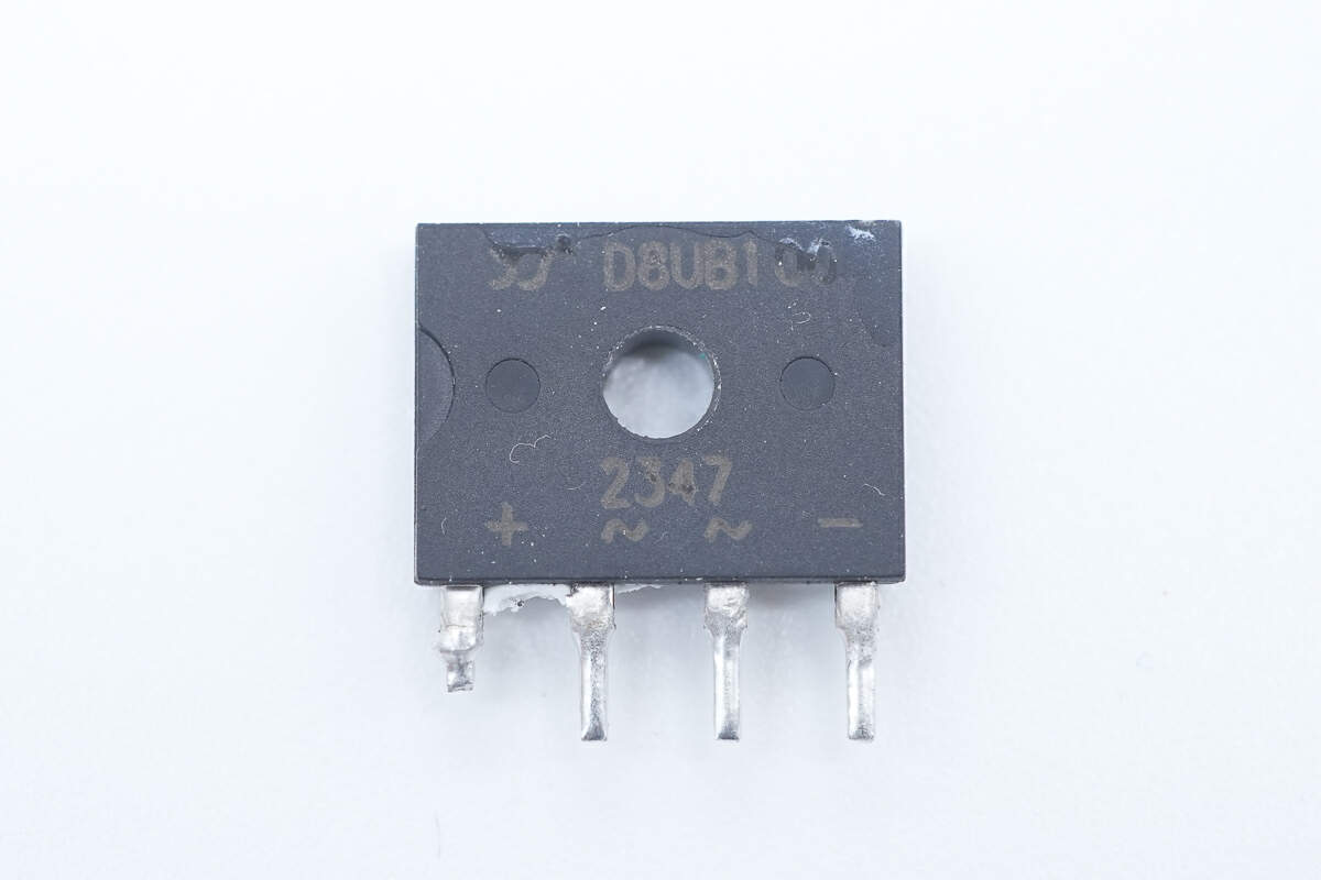
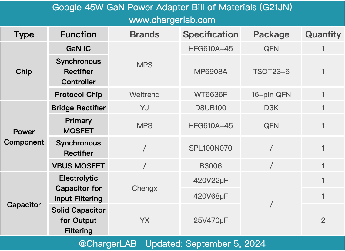
The bridge rectifier is from YJ and adopts D3K package. Model is D8UB100. 8A 1000V.
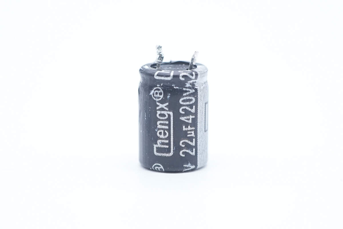
The electrolytic capacitor for input filtering is from Chengx. 420V 22μF.
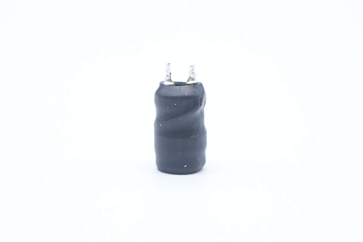
The I-shaped inductor is wrapped with an insulating tube.
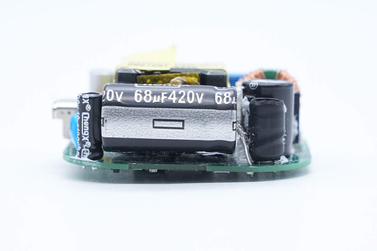
This side has another electrolytic capacitor for input filtering and the capacitor that powers the master control chip.
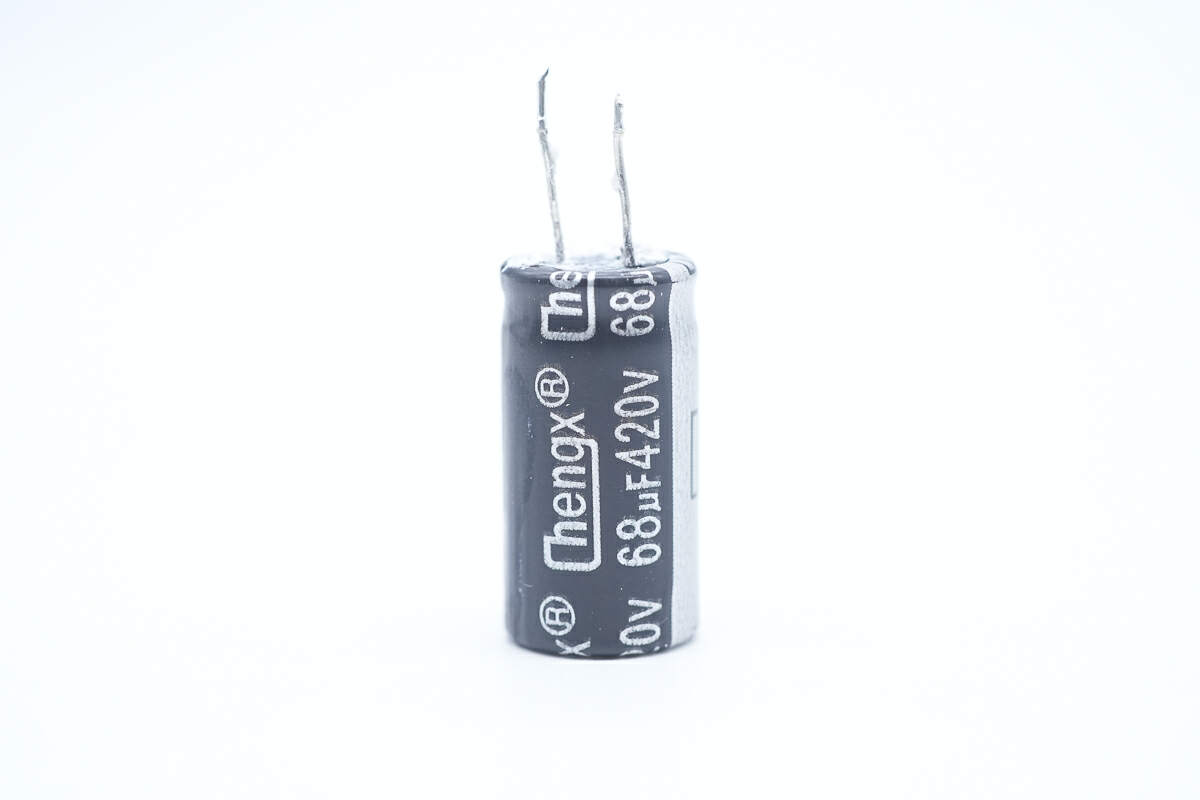
The other electrolytic capacitor for input filtering is also from Chengx. 420V 68μF.
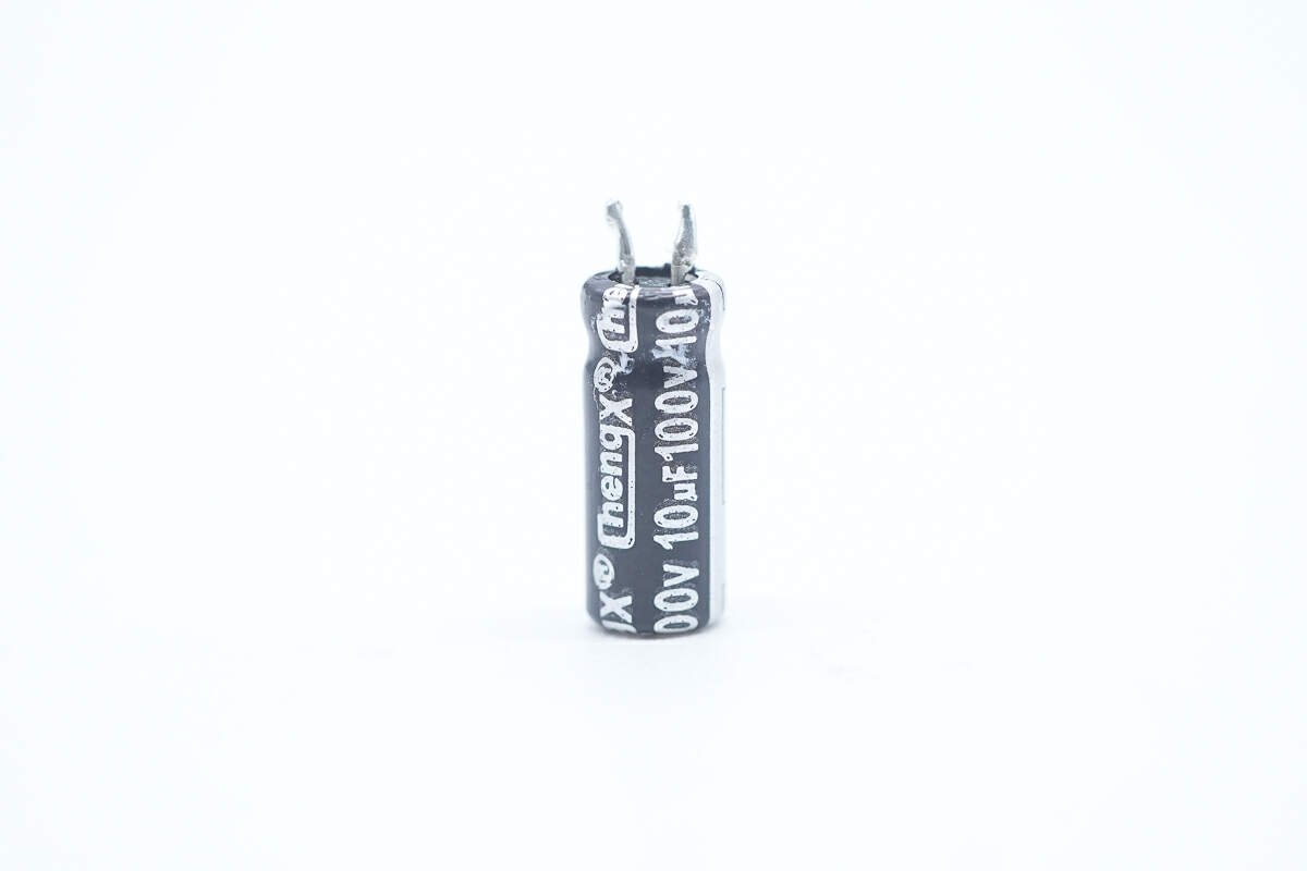
The capacitor that powers the master control chip is from Chengx. 100V 10μF.
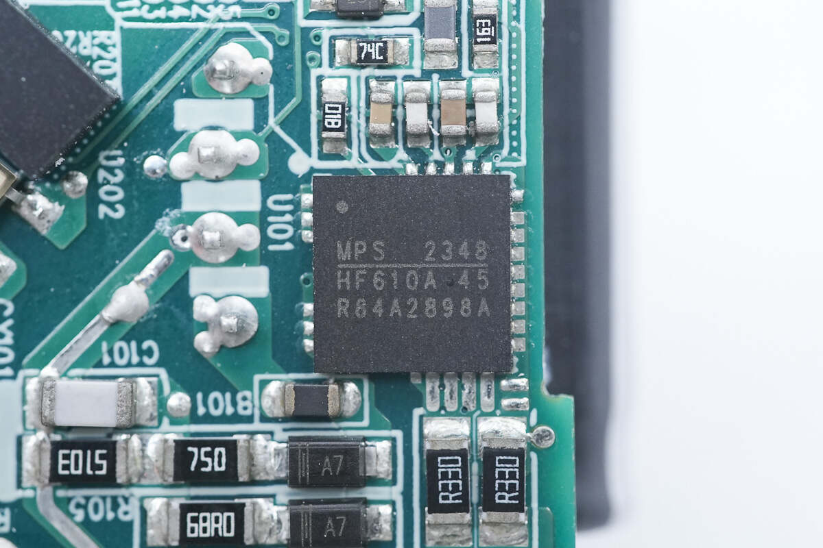
The GaN IC is from MPS and adopts QFN package. It is a QR flyback regulator GaN FET, which is suitable for high performance and high frequency design. It has integrated the 700V/270mΩ GaN FET. It adopts novel patented QR control to eliminate audible noise. It also adopts frequency foldback and burst mode for low light load power consumption.
The ultra-wide VCC range is to support USB-PD applications. It has built-in X-Cap discharger and high voltage start circuit. The standby power consumption is less than 30mW. It adopts peak current mode control, line compensation, and leading edge blanking. Model is HFG610A-45.
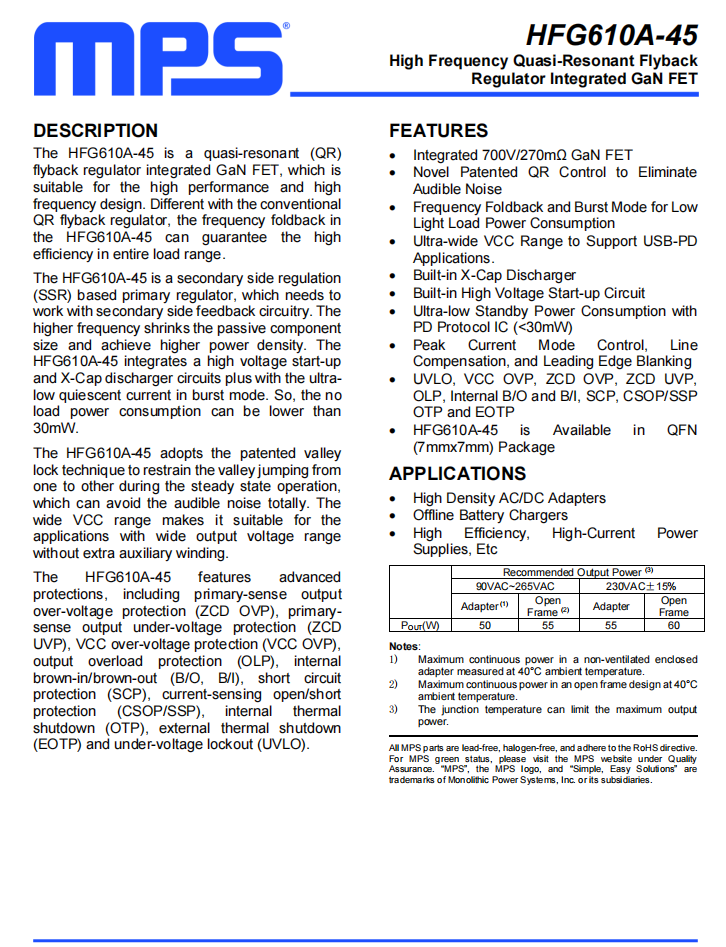
Here is all the information about the MPS HFG610A-45.
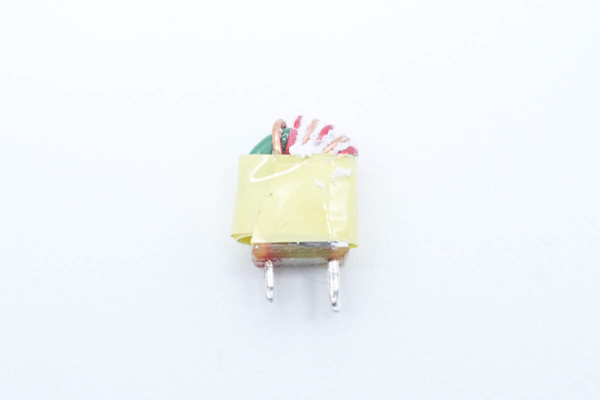
Here is the transformer.
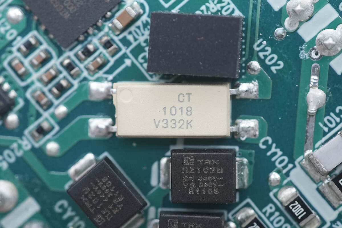
The CT 1018 optocoupler is used for output voltage feedback.
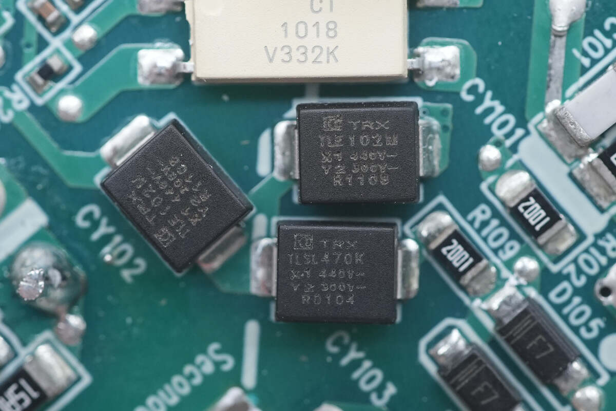
The three SMD Y capacitors are from TR. They are small in size and light in weight, making them very suitable for use in high-density power products such as GaN fast charging. The material numbers are TBY2102ME and TBY2470KSL, respectively.
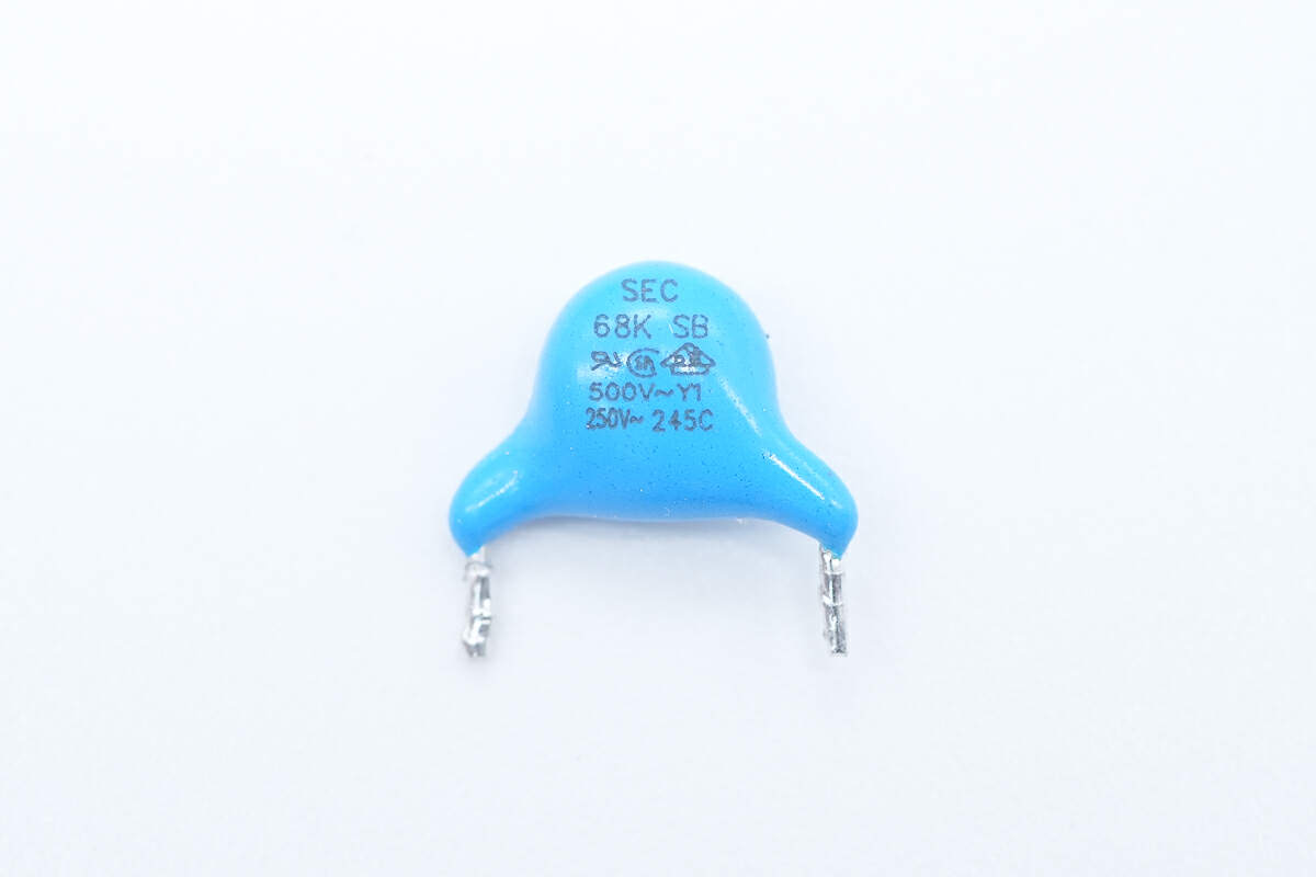
The Blue Y capacitor is from SEC.
The other side of the PCBA module is equipped with a synchronous rectifier and two solid capacitors for output filtering.
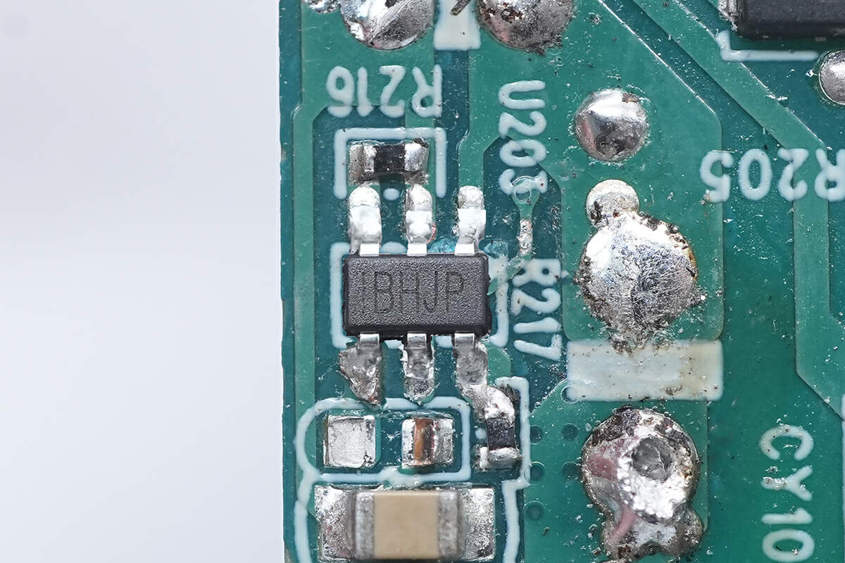
The synchronous rectifier controller marked with IBHJP is from MPS. The maximum operating frequency is 600KHz. It supports multiple working modes, including DCM, CCM, QR, and ACF, supports high-side and low-side applications, and has ringing detection to prevent false activation. Model is MP6908A.
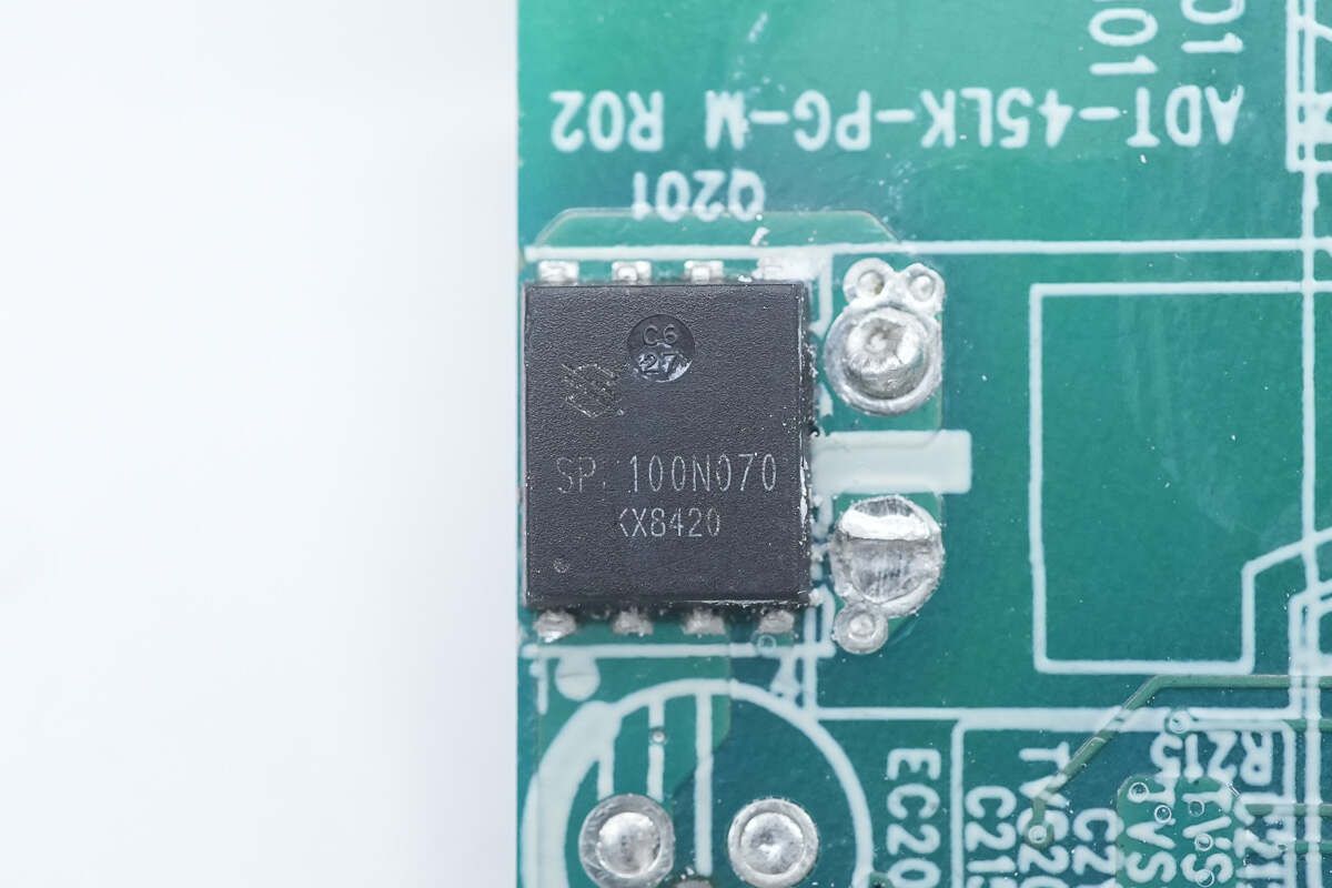
The synchronous rectifier is marked with SPL100N070.
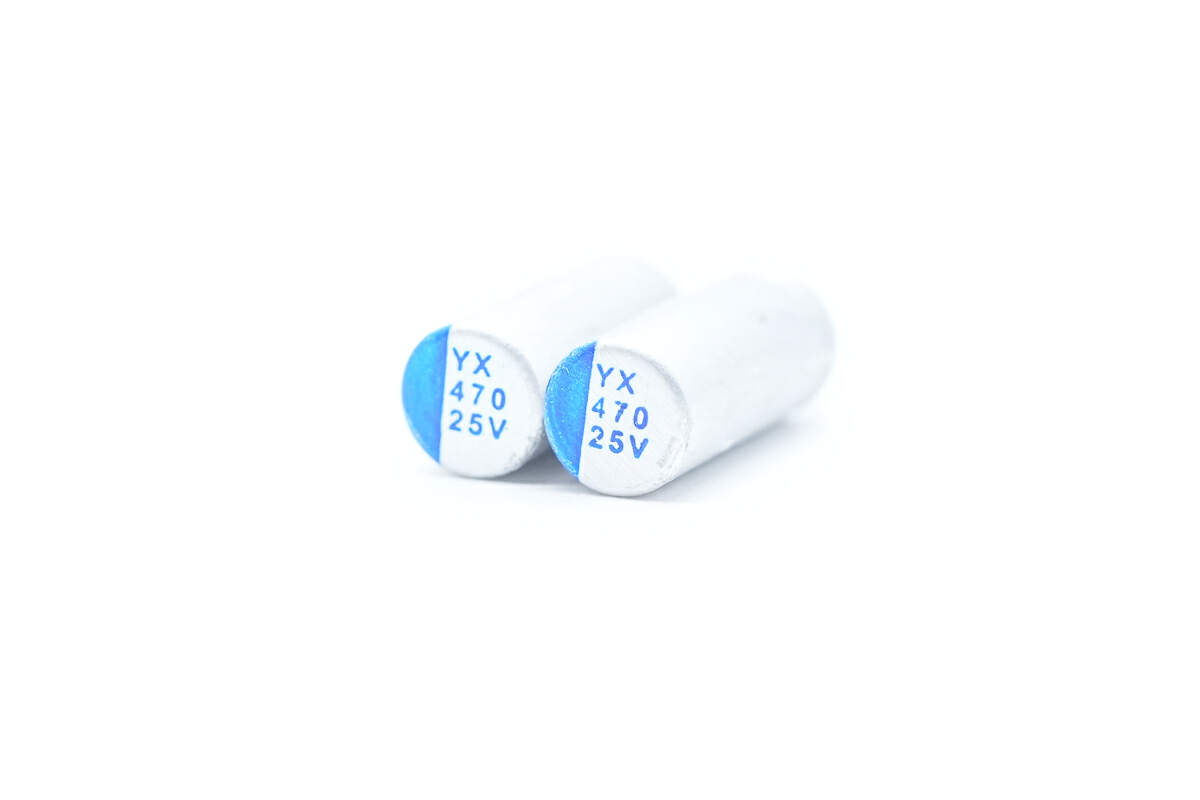
The two solid capacitors for output filtering are from YX. 25V 470μF.
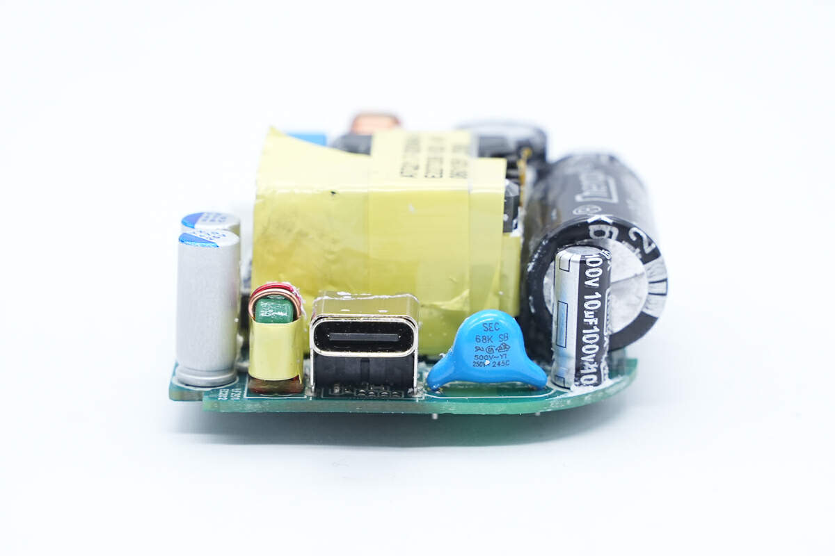
On the output end, the USB-C socket is reinforced with a steel sleeve, the filter inductor on the left is wrapped with tape for insulation, and a Blue Y capacitor is installed on the right.
Here is the filter inductor.
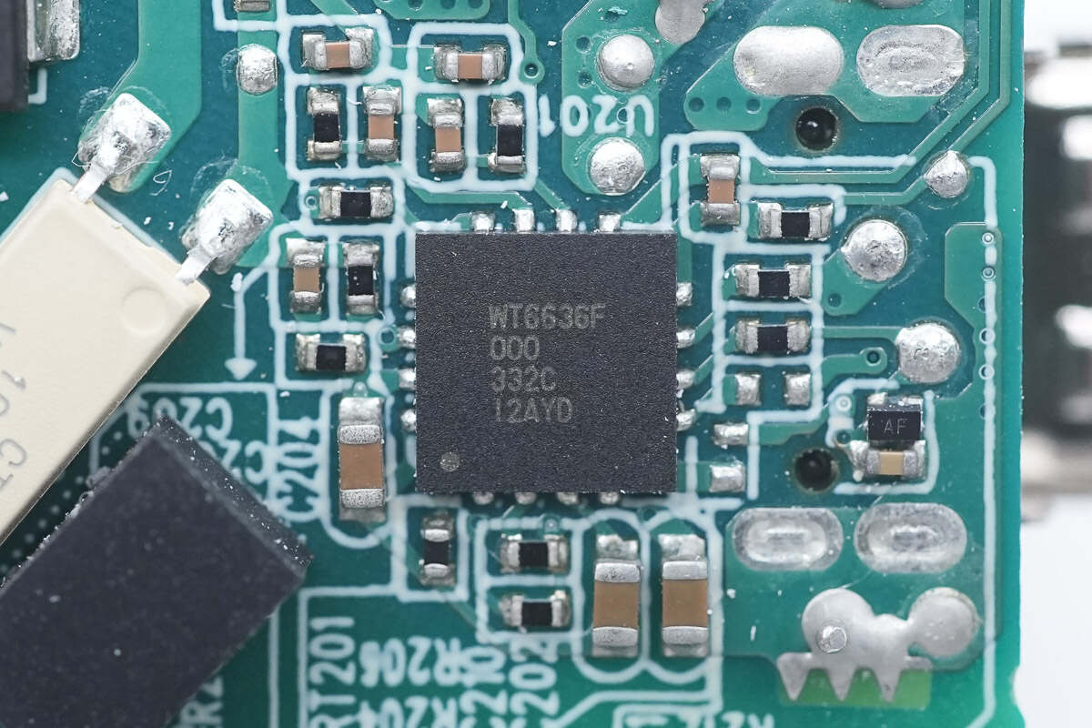
The protocol chip is from Weltrend. It has passed the USB PD3.0 (PPS) certification of the USB-IF Association and has passed the Qualcomm QC4+ certification. It supports USB PD3.0 and PPS, supports line loss compensation, and supports multiple protection functions. It has an integrated 10-bit ADC for voltage and current detection, a built-in 8051 core microcontroller, and a built-in discharge MOSFET. Model is WT6636F.
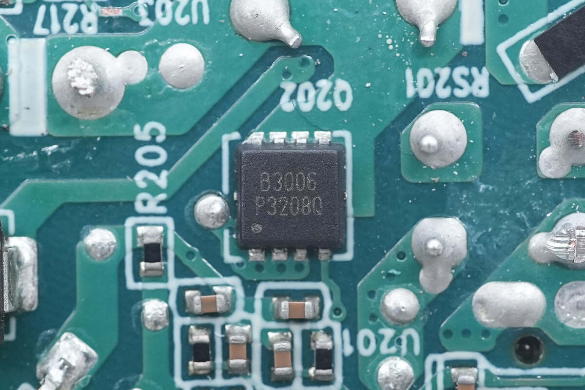
The VBUS MOSFET is marked with B3006.
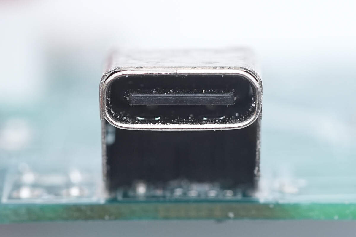
The USB-C port has a black plastic sheet.
Well, those are all components of the Google 45W GaN Power Adapter.
Summary of ChargerLAB
Here is the component list of the Anker 200W desktop GaN charger for your convenience.
It adopts an Australian standard plug, and its appearance design is quite recognizable. And it supports charging protocols such asPD3.0 and PPS. It has four fixed PDOs of 5V3A, 9V3A, 15V3A, 20V2.25A, and three sets of PPS, which are 5-11V3A, 5-16V3A, 5-21V2.25A. Therefore, it is compatible with devices that support PD and PPS fast charging.
After taking it apart, we found the plug is connected to the PCBA module by wires, the gaps between components are filled with potting compound, and the USB-C socket is reinforced with a steel sleeve. The GaN IC is from MPS. It is a QR flyback regulator GaN FET, which is suitable for high performance and high frequency design.
Related Articles:
1. 5000mAh Battery & 23W Charging | Charging Review of Google Pixel 7 Pro
2. Charging Review of Google Pixel 8 Pro
3. Teardown of Unreleased Google 65W Mini Charger