Introduction
Those buying Nintendo Switch Docks should be very careful as fake docks that look just like the real thing have been spotted worldwide.
ChargerLAB has gotten a fake Nintendo Switch Dock, and let's take it apart.
Appearance

This fake Nintendo Switch Dock looks the same as the real one, which is hard to tell.

The dock has a black frosted shell with the NINTENDO SWITCH logo in the center of the front.

The left features an LED indicator as well as a display icon.

There are two black USB-A ports on the side.

There is a USB-C port to charge the Switch, and the whole dock can also serve as a stand.

There is a back cover, inside which is the cable organizer.

Inside the back cover is a square base on the right side.

The square base has one USB-A and one USB-C port on the side, as well as an HDMI output port.

These are the imprints of AC ADAPTER, USB, and HDMI OUT.

The bottom is equipped with non-slip pads. The parameters on the shell show it supports 15V2.6A input and 15V1.2A output and the NOM, NYCE, VCCI, EAC, and CE certifications. However, since it is a fake, the above parameters and certifications are questionable.


Its size is about 172.45 X 102.3 X 50.68 mm (6.78 X 4.02 X 1.99 inches).

The net weight is about 303g (10.68oz).

The ChargerLAB POWER-Z KT002 shows that the USB-A port supports Samsung 5V2A and DCP protocols.

The other USB-A port also supports Samsung 5V2A and DCP protocols.
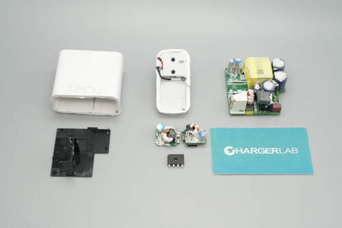
Teardown

The fake dock adopts the same Y-shaped triangle screws as the original.

Take it apart.

These are air intakes for losing heat.

The PCB board is for power supply, HDMI output and USB transfer.

The flat cable socket connecting to the console is at the bottom of the small PCB board.

These are the very few components on the front of the PCB board and the screen printings of chip model, AG9311 for HDMI converter and FE1.1 hub controller for USB HUB.

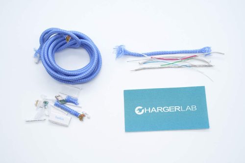
A cable inside the shell connects to the USB-C port, and a wire is for the indicator.

This is the USB-C port.

The cover is supported by springs on the left and right side of the port.

The small PCB board is fixed to the spring bracket at the bottom by screws to act as a cushion.

Here is the spring bracket.

A USB-C connector is soldered on the front of the small PCB board, and the flat cable socket is below.

The USB-C receptacle is fixed and soldered by the vias.

These are the flat cable plugs.

The indicator is connected to the small PCB board with red and black wires.

This is the indicator on the small PCB board.

There are no components on the back.

This is the flat cable plug.

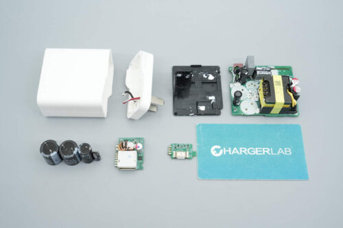
Two converter chips are soldered on the front of the small PCB board, and three buck chips at the bottom, outputting 5V, 3.3V and 1.2V, respectively.

The flat cable socket, capacitor, resistor and MOS tube are on the back. And the USB3.0 is led directly from the host controller.

Here is the flat cable socket connected to the USB-C port.

The ALGOLTEK AG9311 for DP to HDMI output supports DP1.2 input to HDMI1.4 output. It is a USB-C to HDMI solution, supporting 4K30Hz output.

The 27.000 MHz crystal is used to provide the clock signal for the AG9311.

The USB HUB is from CoreChips, Shenzhen, with the model SL2.2s. It is a USB2.0 HUB chip that supports four USB ports and BC1.2 mode. The 12.000MHz crystal is used to provide the clock signal.

The USB-C receptacle is fixed and soldered by the vias for input.

The USB-C input is transmitted to the synchronous buck circuit through a VBUS switch.

The VBUS switch is from AOS, with model AO4805. It is a dual PMOS with 30V withstand voltage and 10mΩ thermal resistance in an SO8 package.

Synchronous buck converter for 5V buck output has a screen printing of 3683 in the SOT23-6 package, with a 4.7μH inductor on the right.

The Synchronous buck converter, JW5250A from Joulwatt, for 3.3V buck output has screen printing of JWM3L, which has an input of 6V and output of 1A. It adopts the SOT23-6 package, below which is a 4.7μH inductor.

The 1.2V and 3.3V synchronous buck converters have the same model, both from Joulwatt.

This is the USB3.0 receptacle, fixed and soldered by the vias.

The HDMI receptacle is alos fixed and soldered by the vias.

The USB2.0 receptacles are the same as the previous two.

It is the outlet that connects to the indicator.

The MLCC filter capacitor for the USB 3.0 port is in the 1210 package.

That's all for the teardown.
Summary of ChargerLAB
This fake Nintendo Switch Dock looks just like the real one, and it's difficult to tell from the appearance. After taking it apart, ChargerLAB found that this dock uses only a DP to HDMI converter to convert the DP signal into HDMI signal output and a built-in HUB chip for USB2.0 expansion.
Compared to the original dock, the overcurrent protection chip of the USB-A port is omitted, while the buck circuit can not meet the needs of connecting high-power devices. Besides, many other chips are also not saved. So the security can not be guaranteed.
Related Articles:
1. Charging Compatibility Test of Nintendo Switch OLED Model (20-100W)
2. Charging Compatibility Test of Nintendo Switch TV mode (20-100W)
3. Teardown of Seagate Firecuda Gaming Dock With 4TB External Hard Drive