Introduction
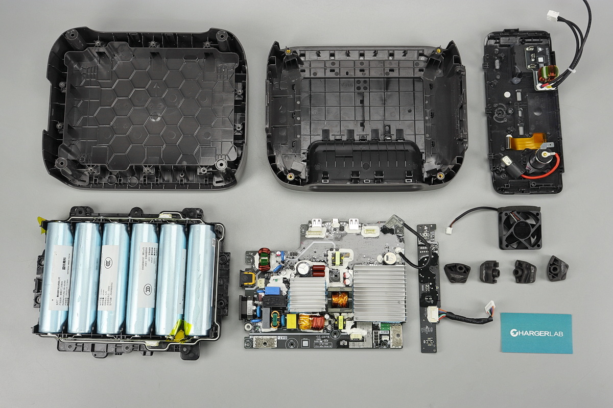
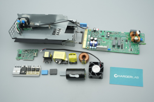
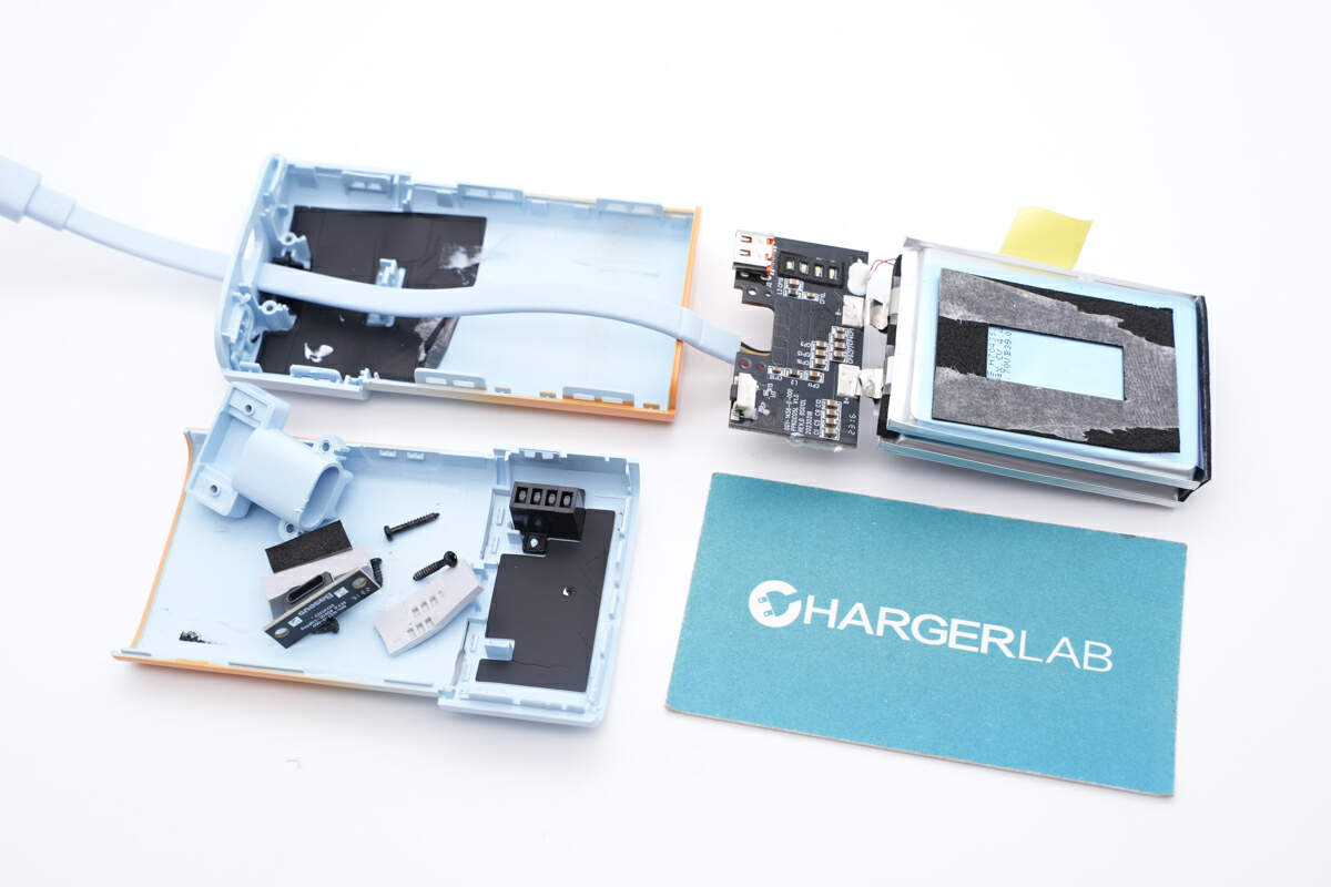
ECOFLOW has launched a new RIVER 3 series power station. This power station applies GaN technology. Its size and weight have significant advantages over traditional products, and the conversion efficiency has been greatly improved. Not only is it lighter and easier to carry, but the discharge capacity is also stronger, and the discharge time for different loads is significantly extended.
The ECOFLOW RIVER 3 power station weighs only 3.5 kg. It only takes 43 minutes to charge from 0 to 80% using an AC power source, making emergency use easier. It also supports solar and car charger input. It has a built-in automotive-grade full-ear lithium iron phosphate battery.
The battery pack is dustproof and waterproof with IP54 protection. The built-in inverter supports 300W output power and 600W up-conversion drive. The USB-C port supports 100W fast charging output to meet the charging needs of laptops and phones. Next, let's take it apart to see its internal components and structure.
Product Appearance
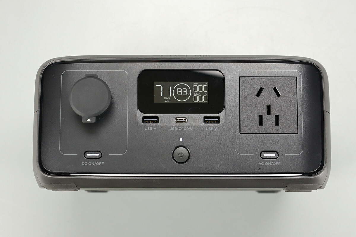
The ECOFLOW RIVER 3 power station is compact and only 113mm in height, making it easy to carry. There are openings on the left and right sides for air intake of the cooling fan.
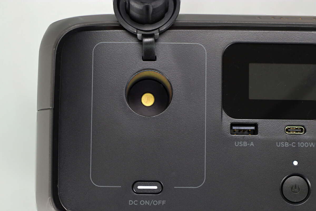
There is a cigarette lighter interface on the left side, with a cover to prevent dust and a switch button at the bottom. There is an indicator light on the button to indicate the output status.
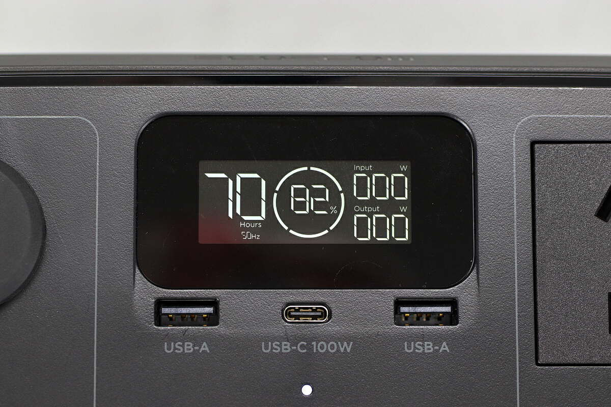
There is an LCD screen on the front that can display the remaining usage time, remaining power, input and output power. There are two USB-A ports and one USB-C port at the bottom.
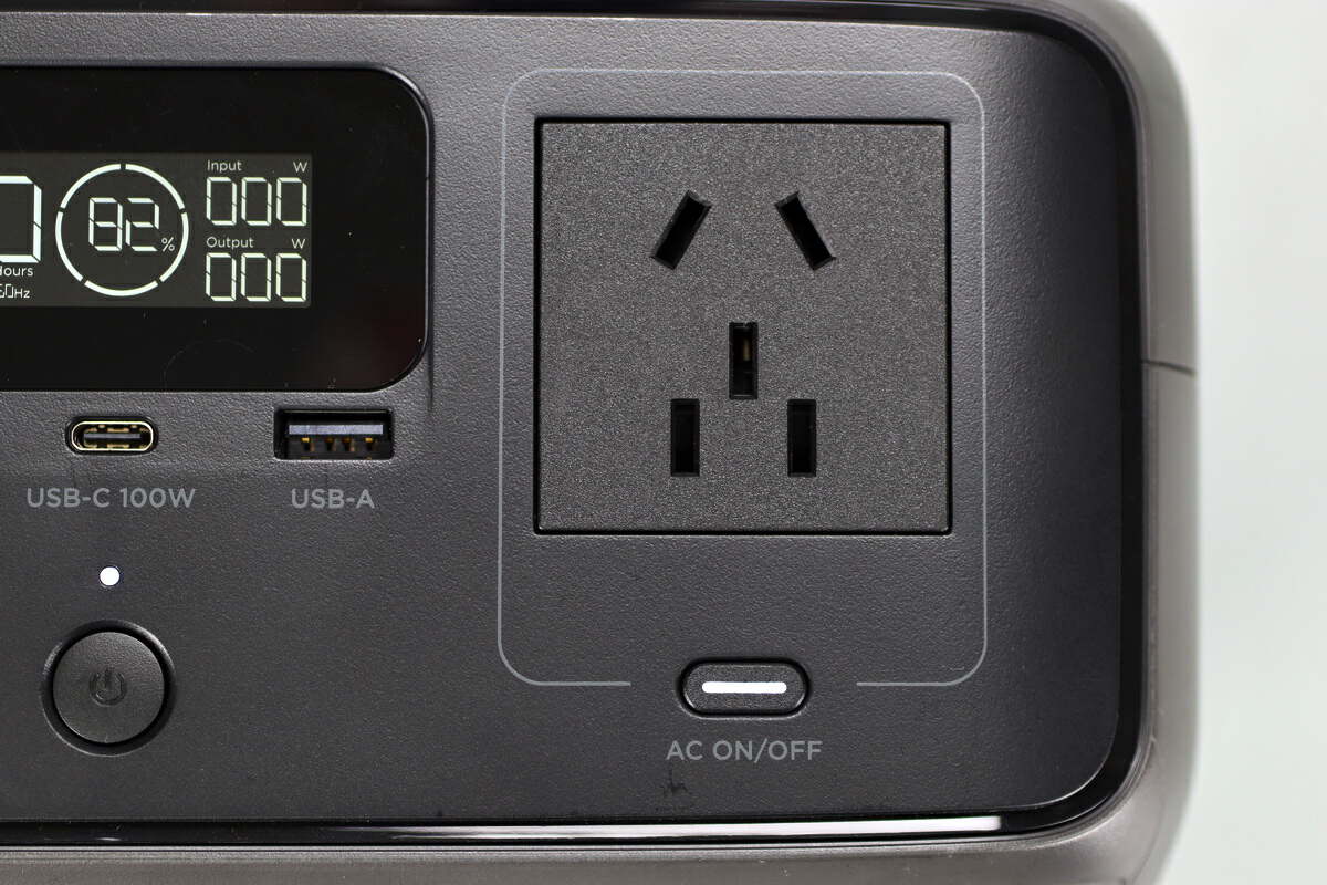
There is an AC outlet on the right and a switch button on the bottom.

The AC output voltage was measured to be 218.6V.
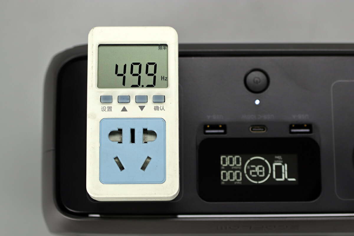
The output frequency is 49.9Hz.
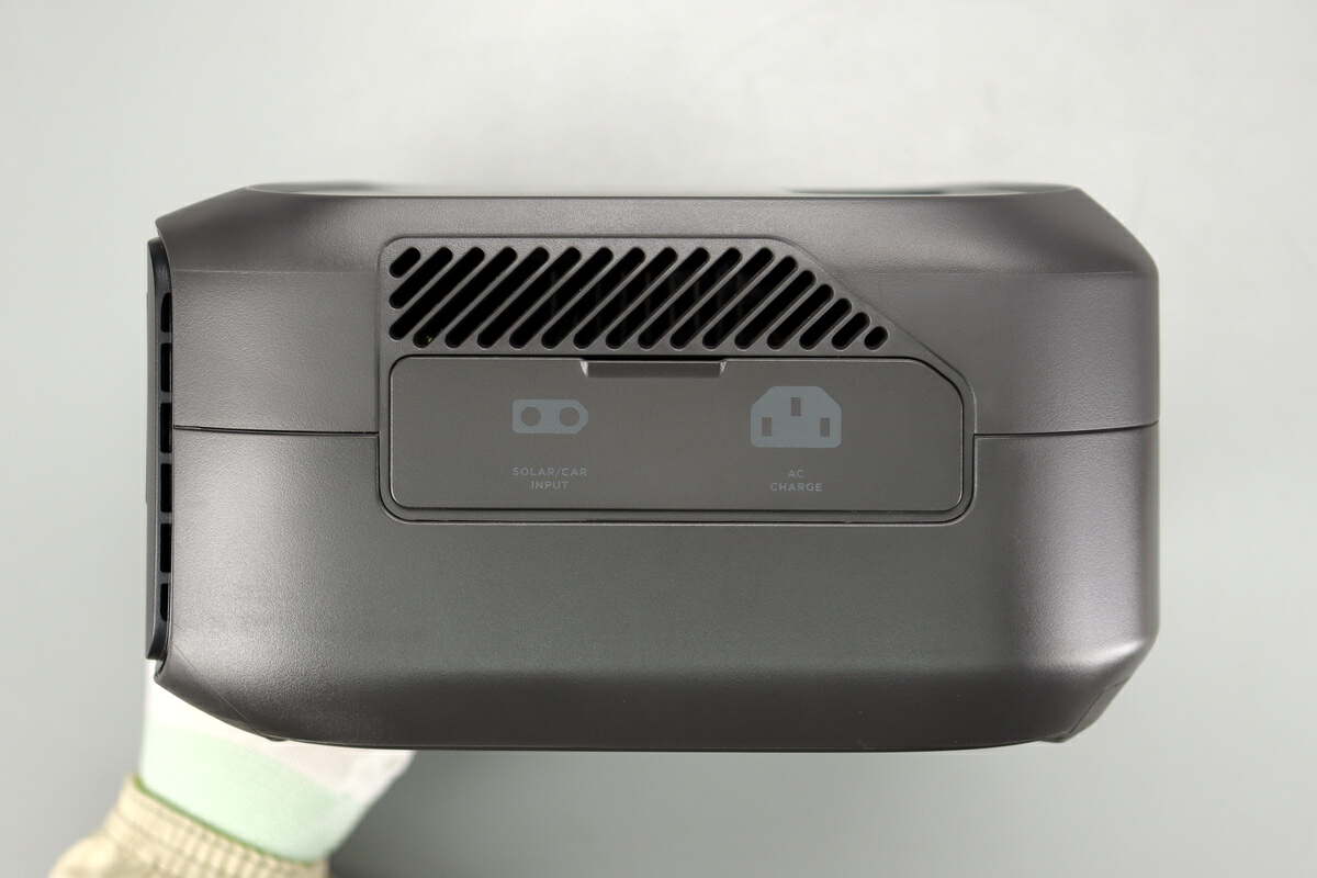
There are air intakes and a cover on this side.
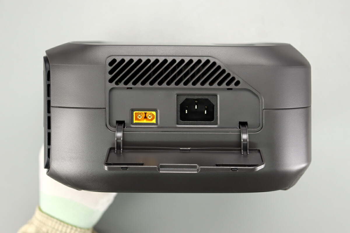
There is a DC input interface and an AC input interface inside the cover.
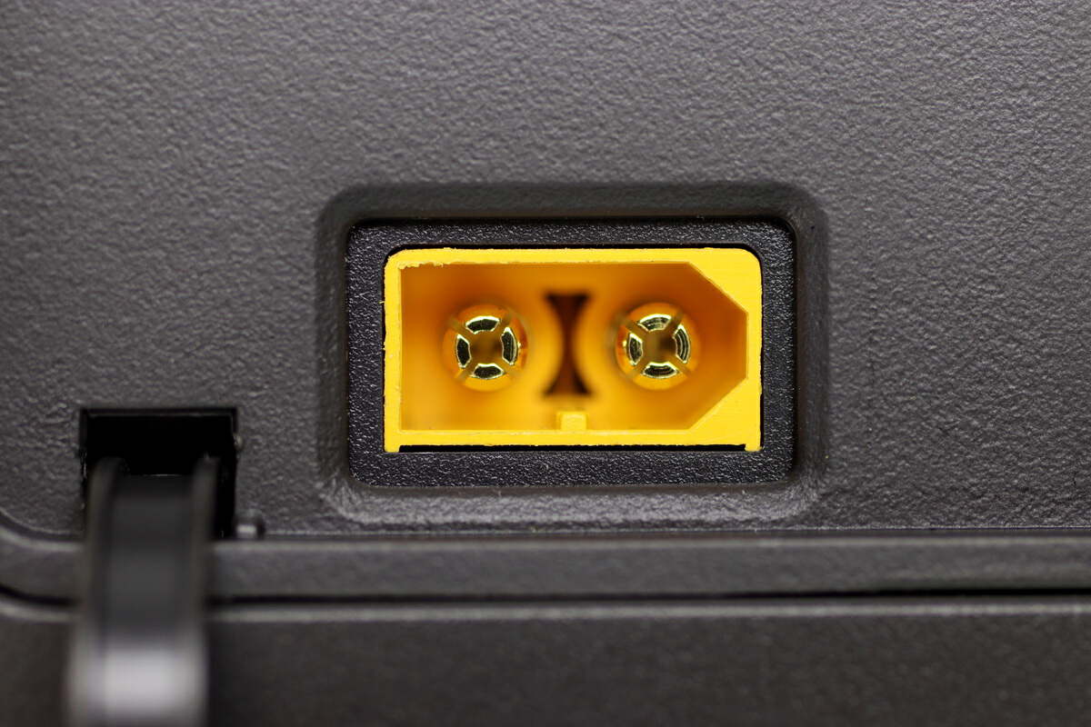
The DC input interface is an XT60 interface.
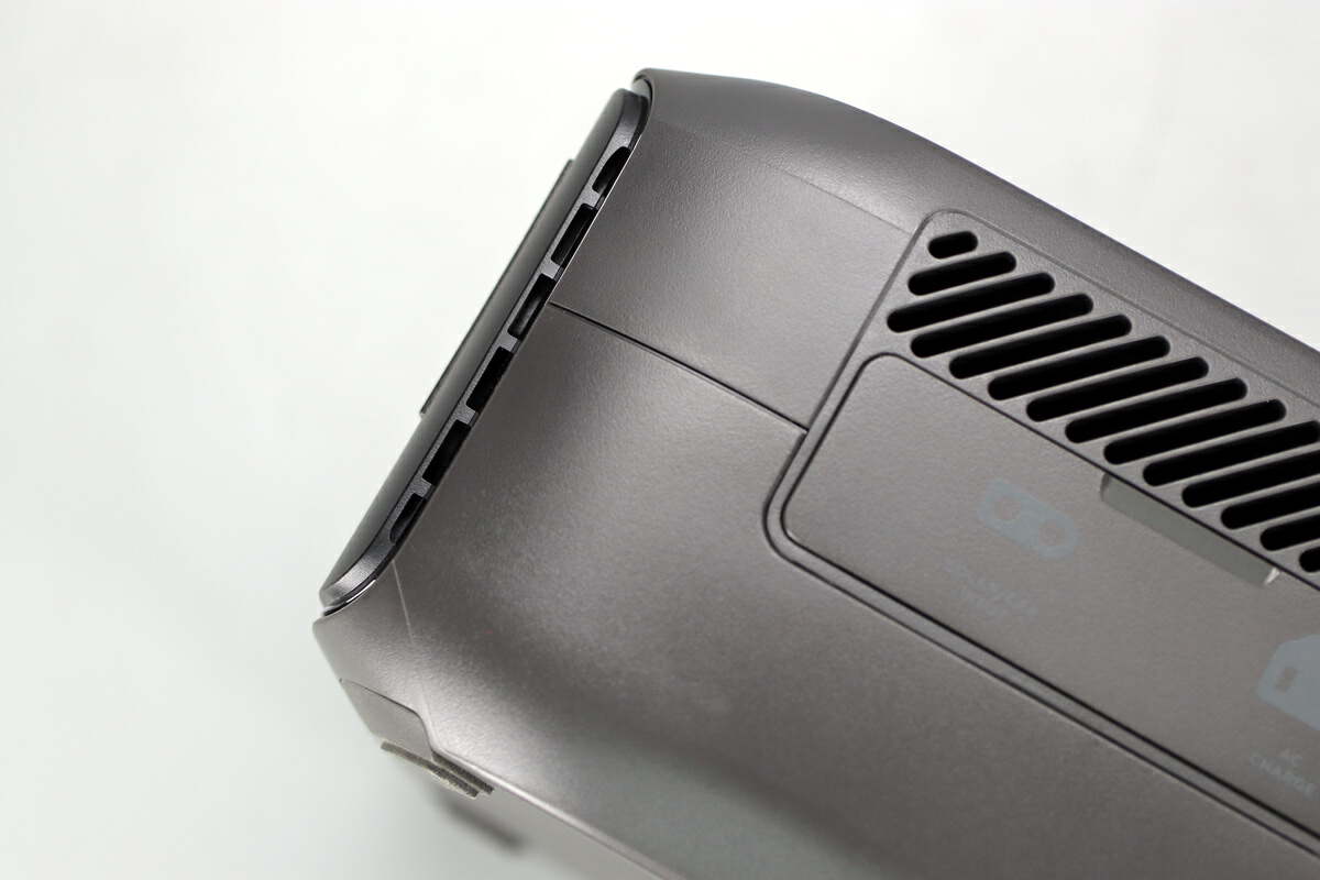
Close-up of the air intake.
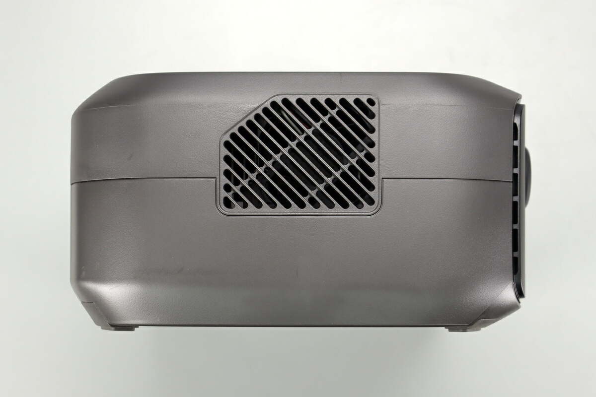
There is a cooling fan outlet on the other side.

Close-up of the air outlet.

The top is flat, and there is an integrated handle at the rear.

ECOFLOW is printed on the top front.

There is also an integrated carry handle at the rear.
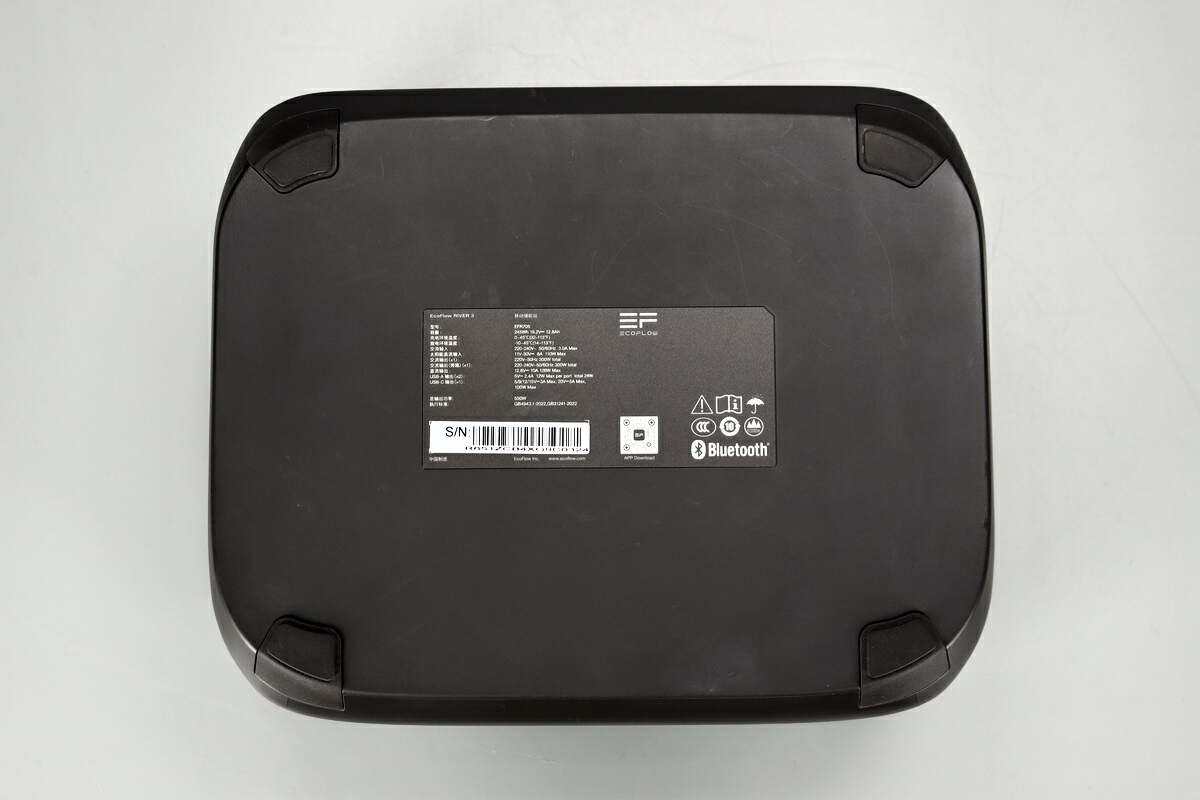
The bottom has non-slip mats and an information label.
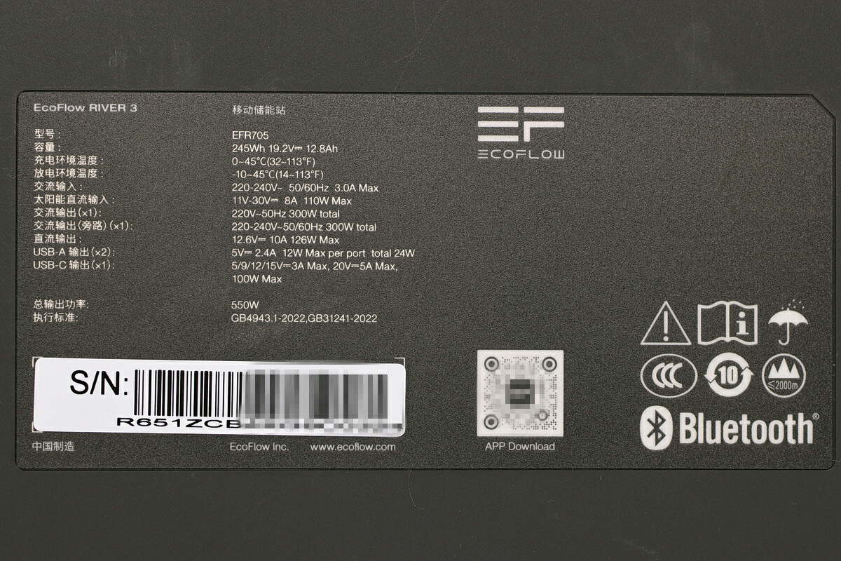
Model: EFR705
Capacity: 245Wh 19.2V 12.8Ah
Charging environment temperature: 0-45℃
Discharging environment temperature: -10-45℃
AC input: 220-240V~ 50/60Hz 3A Max
Solar DC input: 11V-30V 8A 110W Max
AC output (x1): 220V~50Hz 300W total
AC output (bypass) (x1): 220V-240V~50-60Hz 300W total
DC output: 12.6V 10A 126W Max
USB-A output (x2): 5V 2.4A 12W Max per port total 24W
USB-C output (x1): 5/9/12/15V3A, 20V5AMax, 100W Max
Total output power: 550W
Teardown
Next, let's take it apart to see its internal components and structure.
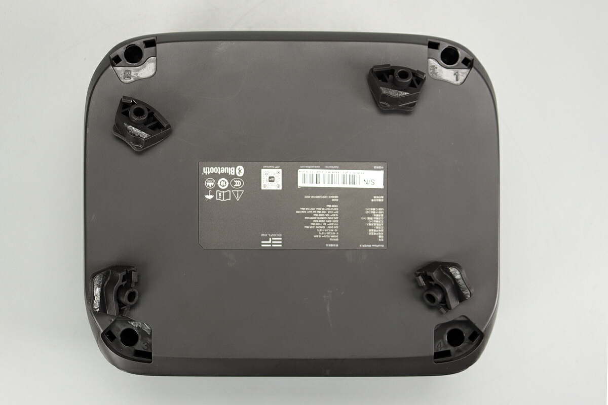
First remove the non-slip pads at the four corners and unscrew the internal fixing screws.
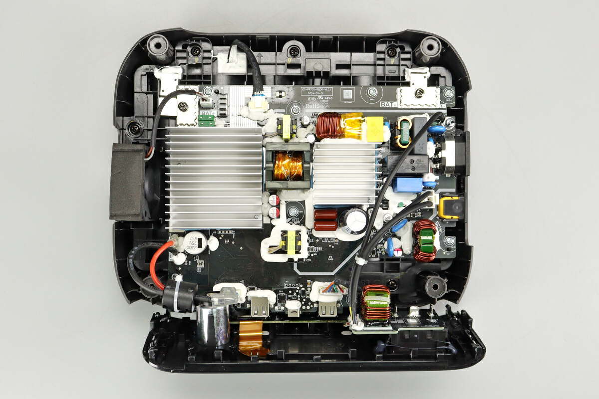
Open the cover, there is a bidirectional inverter module inside and a cooling fan on the left.
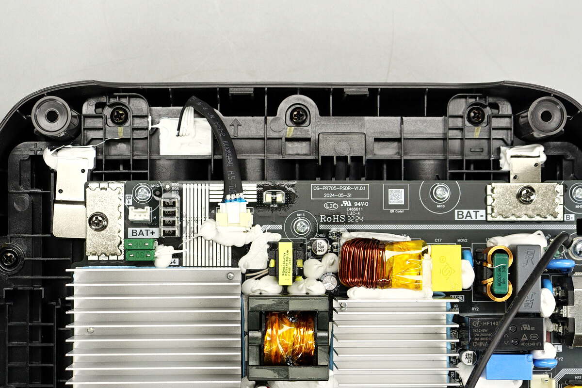
The bidirectional inverter module is fixed with screws.
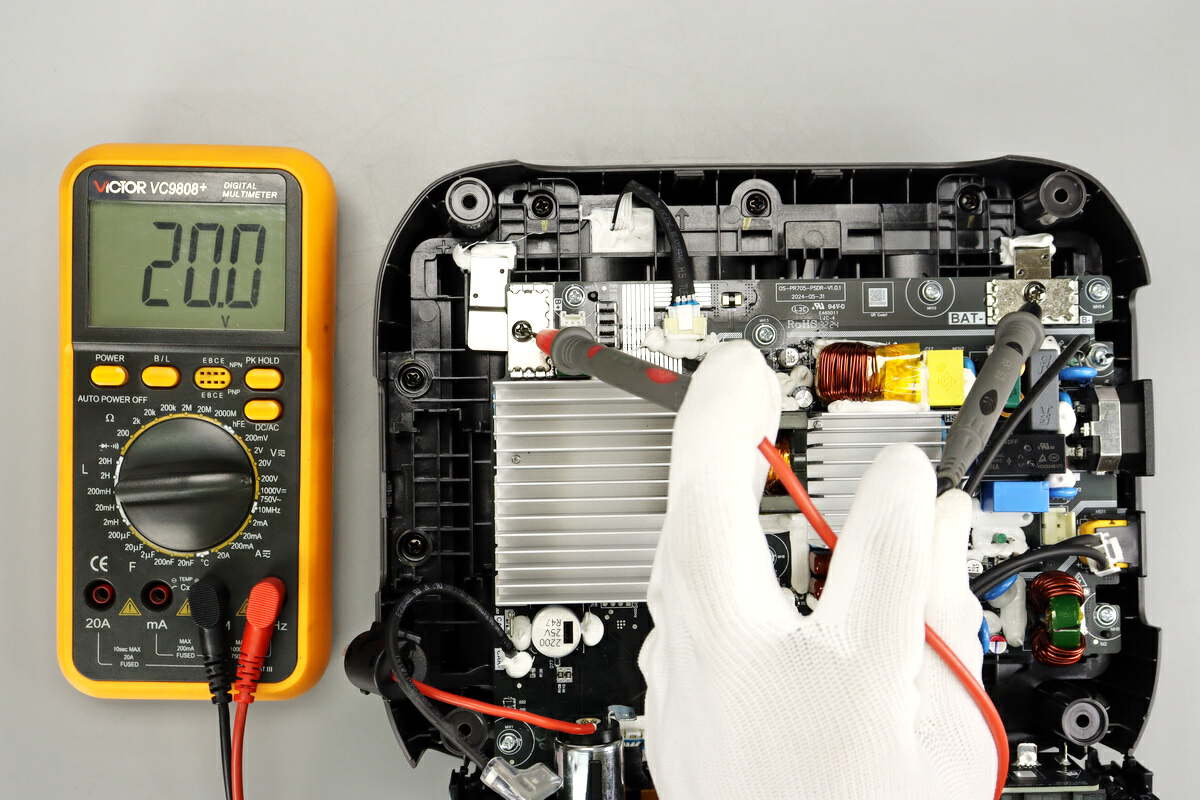
The battery pack voltage was measured to be approximately 20V.
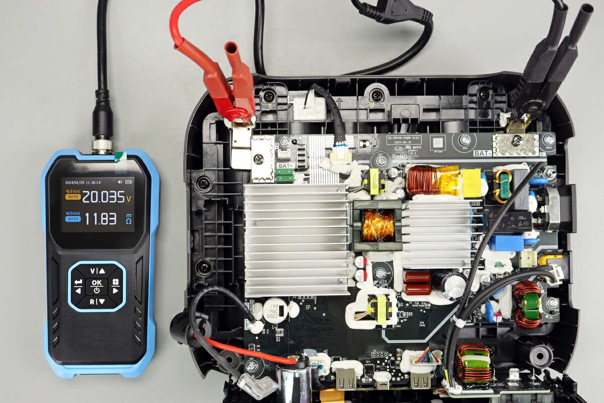
The internal resistance of the battery pack is about 11.83mΩ.
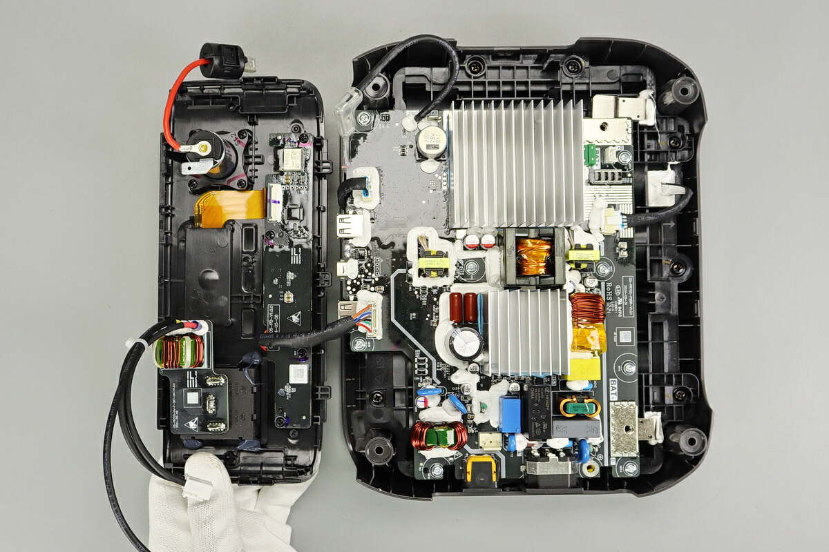
Disconnect the connector of the cigarette lighter interface and the AC socket, it can be seen that the PCBA module is inside.
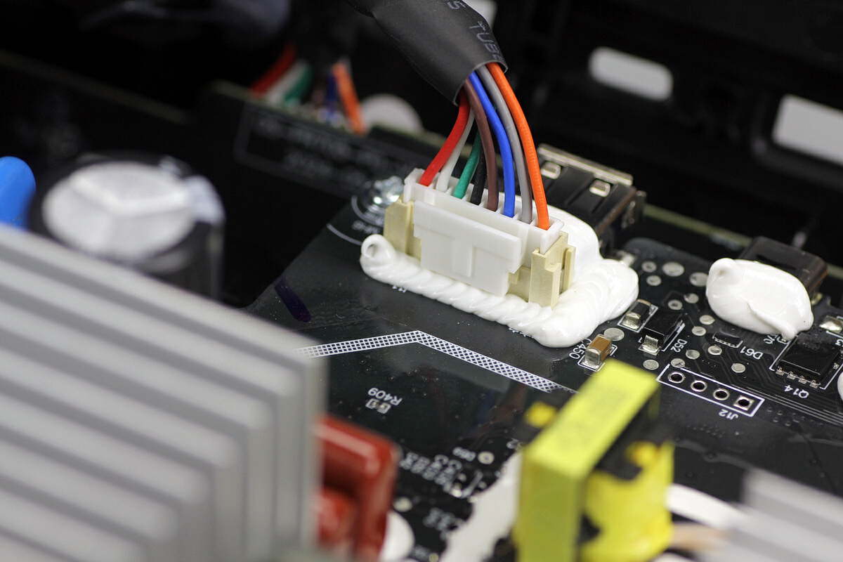
The connector and USB-A port are reinforced with glue.
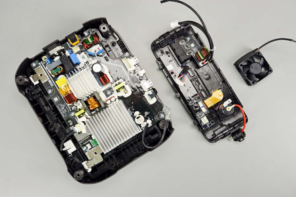
Disconnect the connector and remove the front panel and cooling fan.
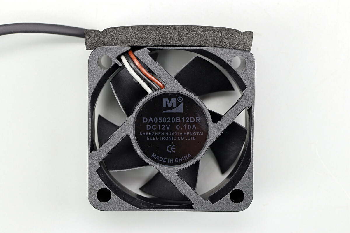
The cooling fan is from Huaxia Hengtai. 12V 0.1A. Model is DA0502B12DR.
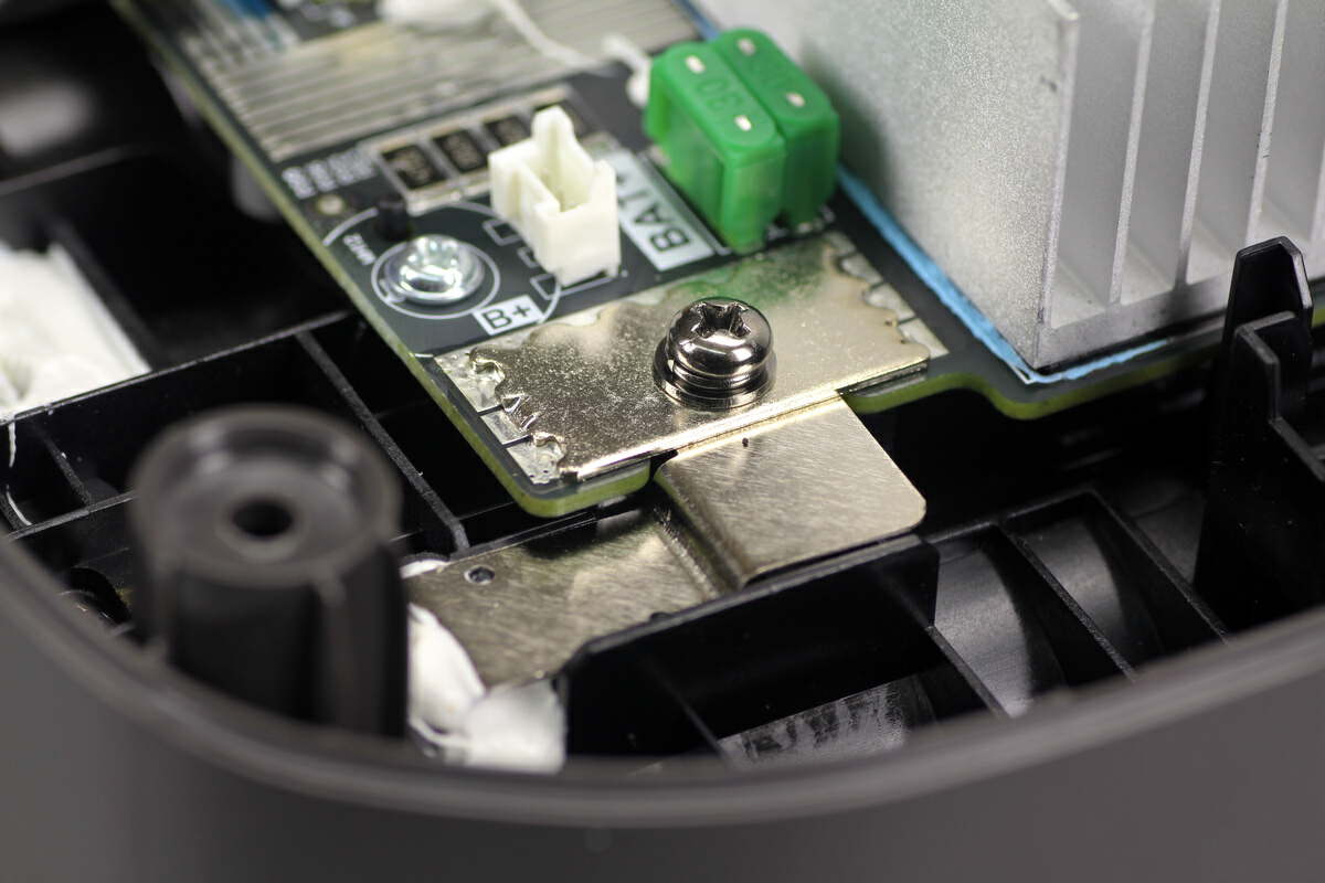
The positive nickel sheet of the battery pack is fixed with a screw.
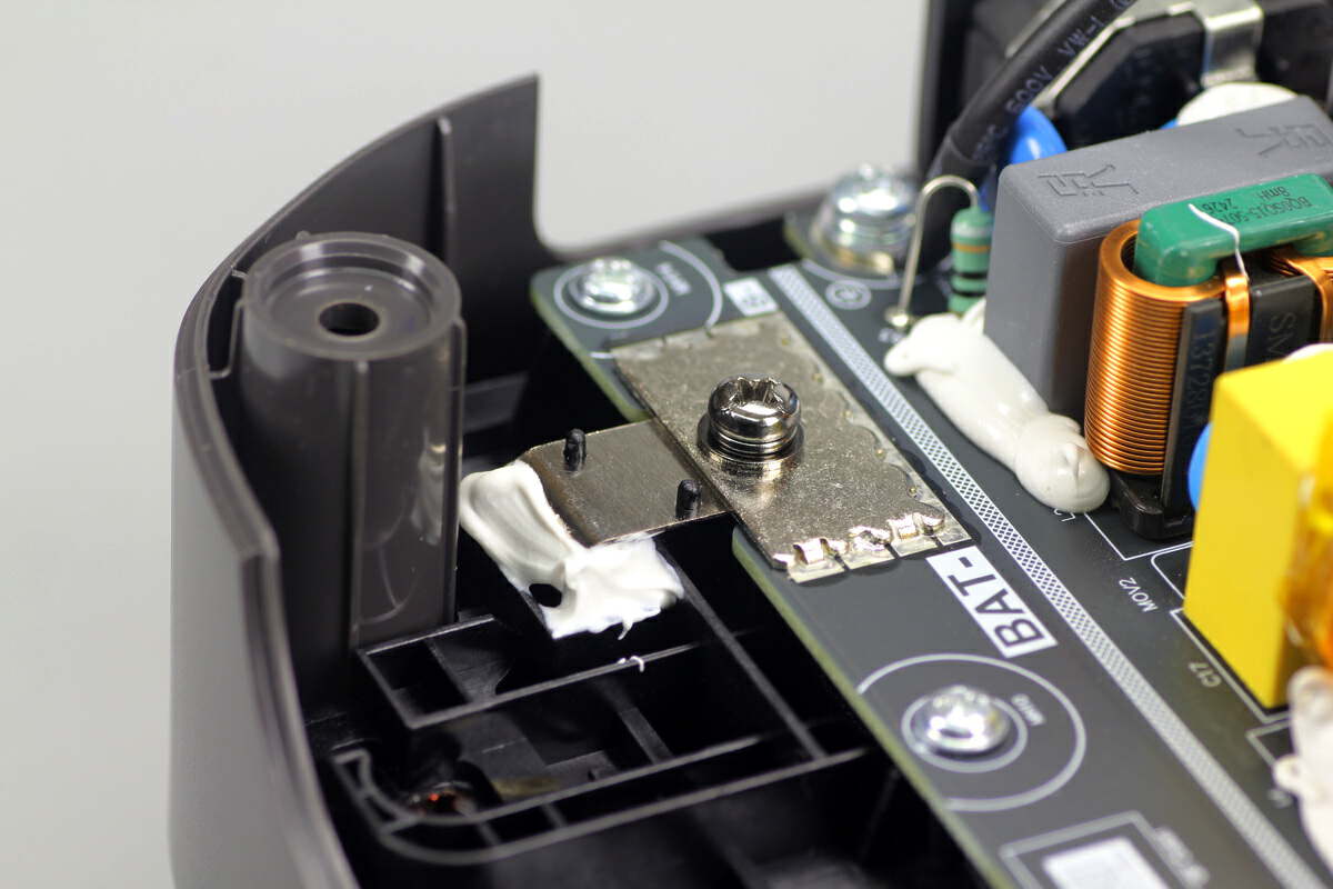
The negative nickel sheet of the battery pack is also fixed with a screw.
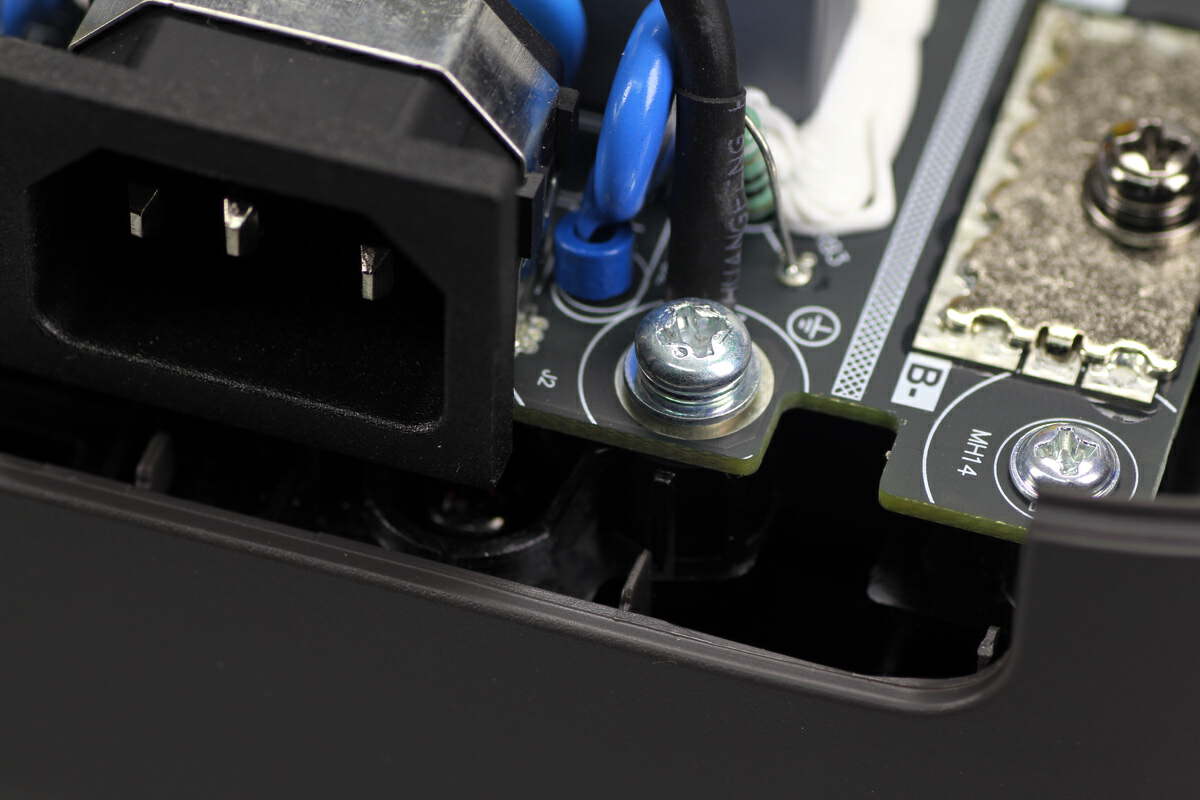
The PCBA module is fixed with screws.
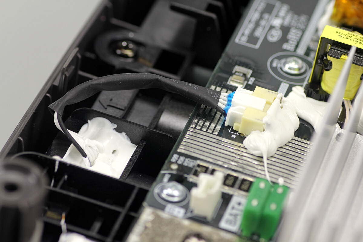
This is the cable used to detect the battery split voltage and battery temperature.
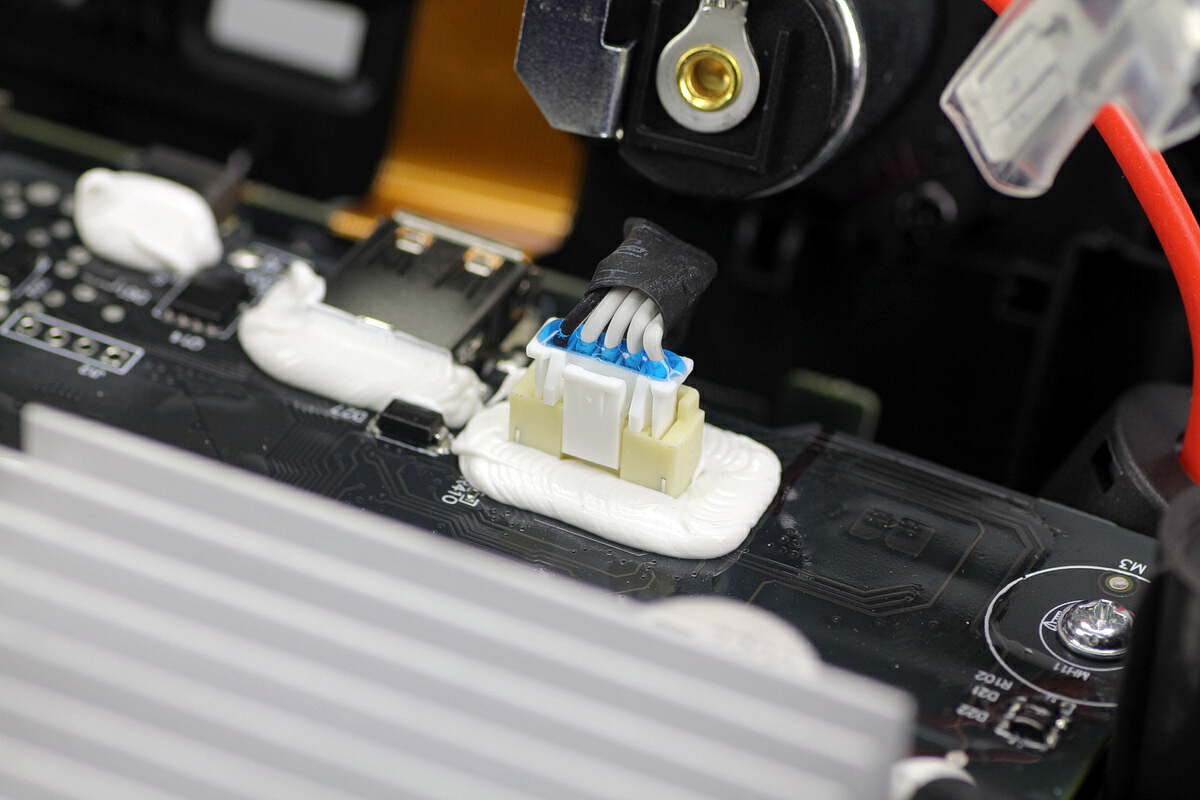
Another cable is also used to detect the battery split voltage and battery temperature.
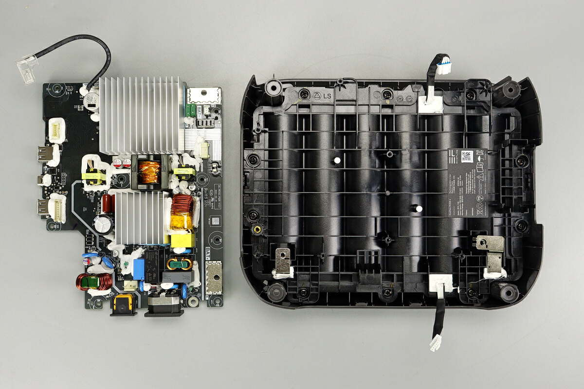
Unscrew the fixing screws and remove the PCBA module. The bottom is the battery pack with an information label attached.
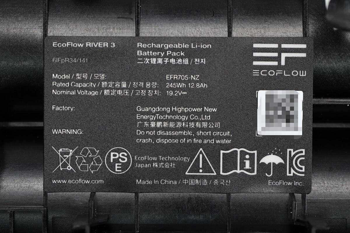
Model is: EFR705-NZ
Rated capacity: 245Wh 12.8Ah
Rated voltage: 19.2V
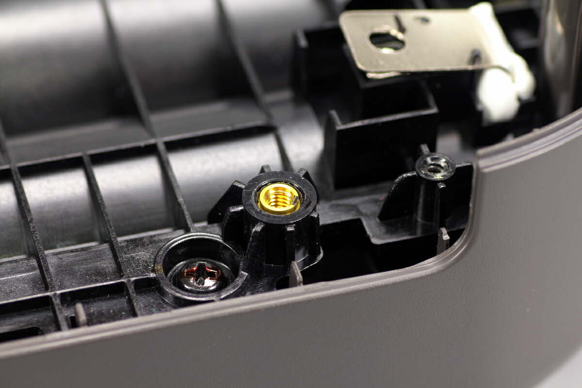
This is the injection molded copper screw used to fix the bidirectional inverter module.
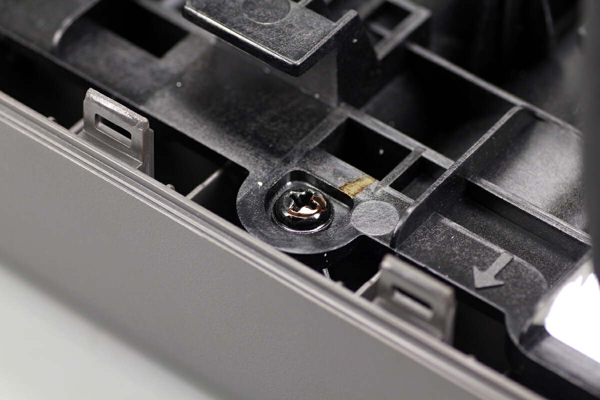
The battery pack cover is fixed with screws.
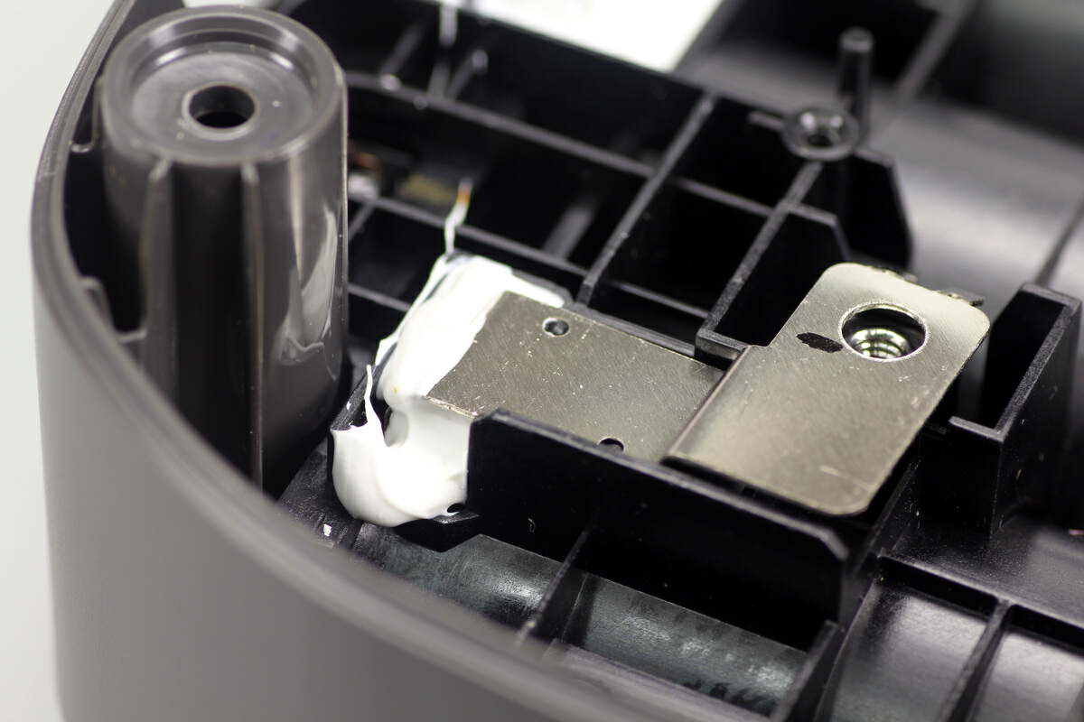
The connection between the positive nickel sheet of the battery pack and the cover is sealed with glue.
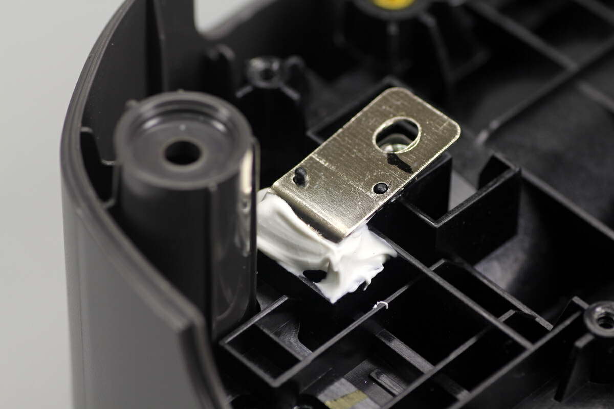
The connection between the negative nickel sheet of the battery pack and the cover is sealed with glue.
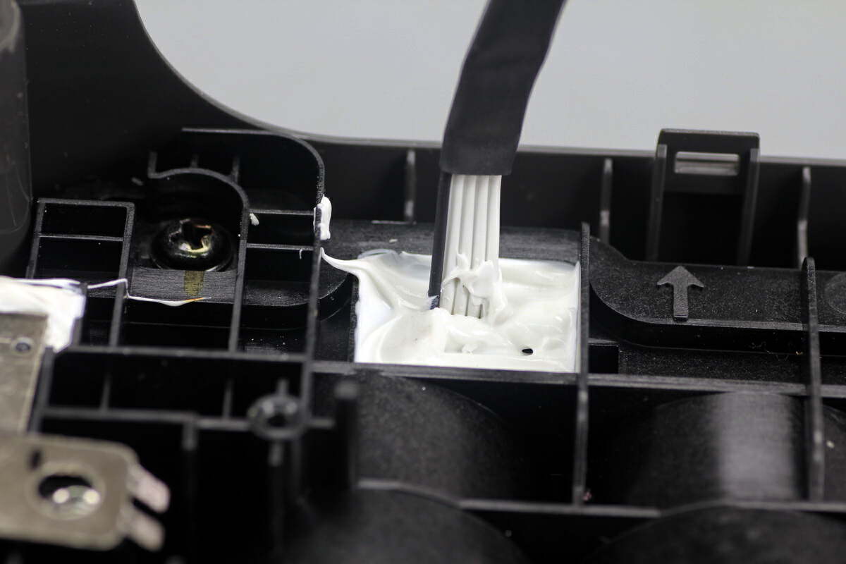
The connection between the cable used to detect the battery split voltage and battery temperature and the cover is sealed with glue.

The other cable is also sealed with glue.
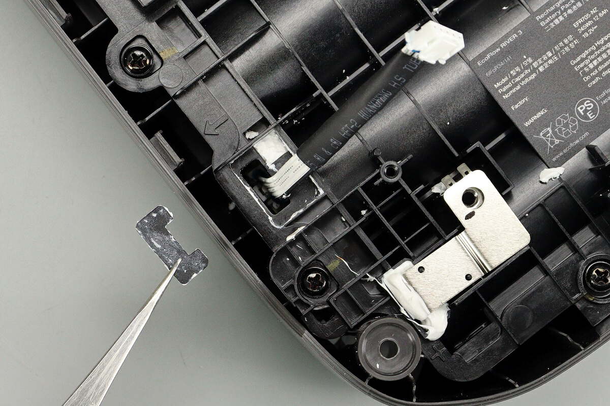
The battery pack voltage sampling wires are fixed by plastic sheets and glue.
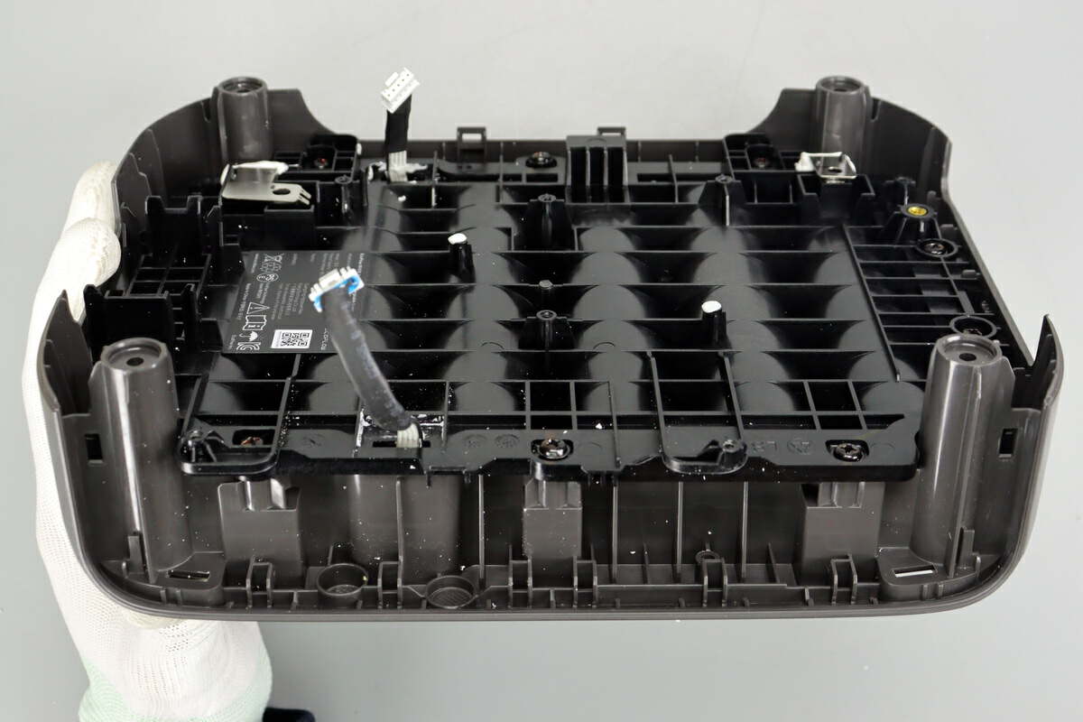
The battery pack cover is fixed to the housing by screws.
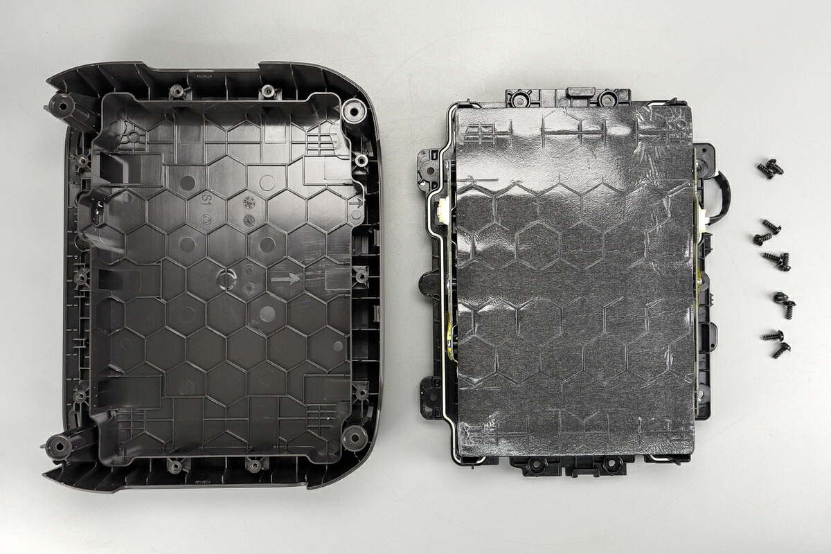
Unscrew the fixing screws and remove the battery pack from the shell. The battery pack is fixed with double-sided foam tape, and there are hexagonal reinforcement ribs inside the shell.
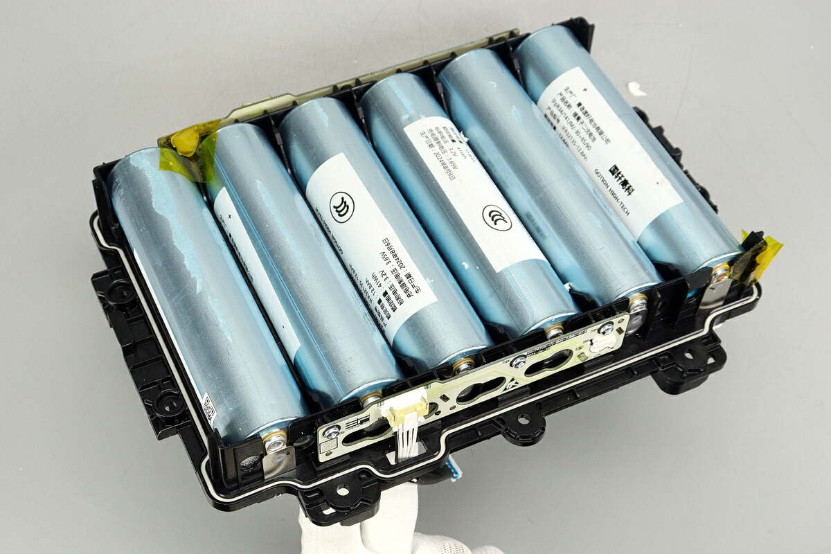
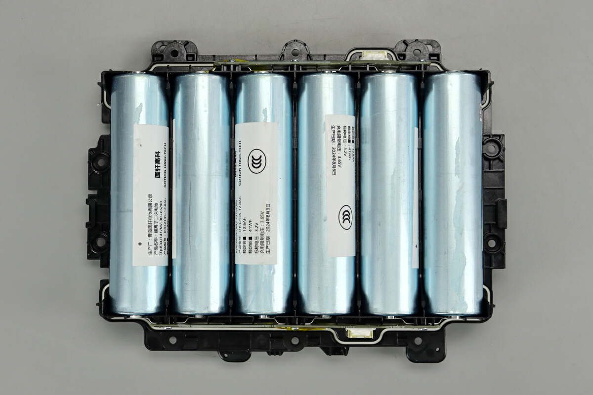
The battery pack is composed of six lithium-iron phosphate batteries connected in series.
The batteries are insulated by plastic frames.

The battery pack sealing rubber rings are used to prevent dust and water.
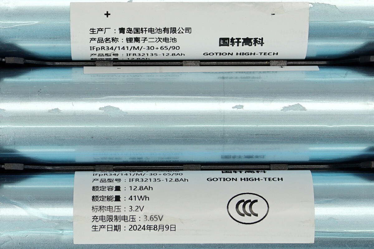
The lithium iron phosphate batteries are from Gotion High-tech. The nominal voltage is 3.2V, the charging limit voltage is 3.65V, the rated capacity is 12.8Ah, and the rated energy is 41Wh. Model is IFR32135-12.8Ah.
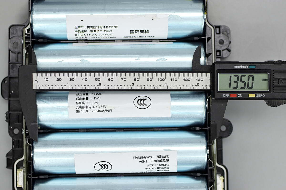
The length of the battery is about 135 mm (5.31 inches).
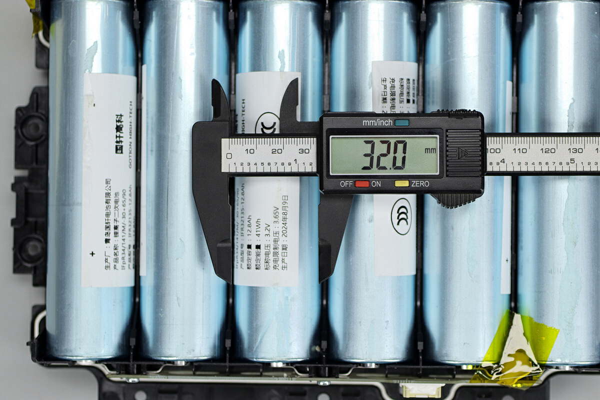
The diameter is about 32 mm (1.26 inches).
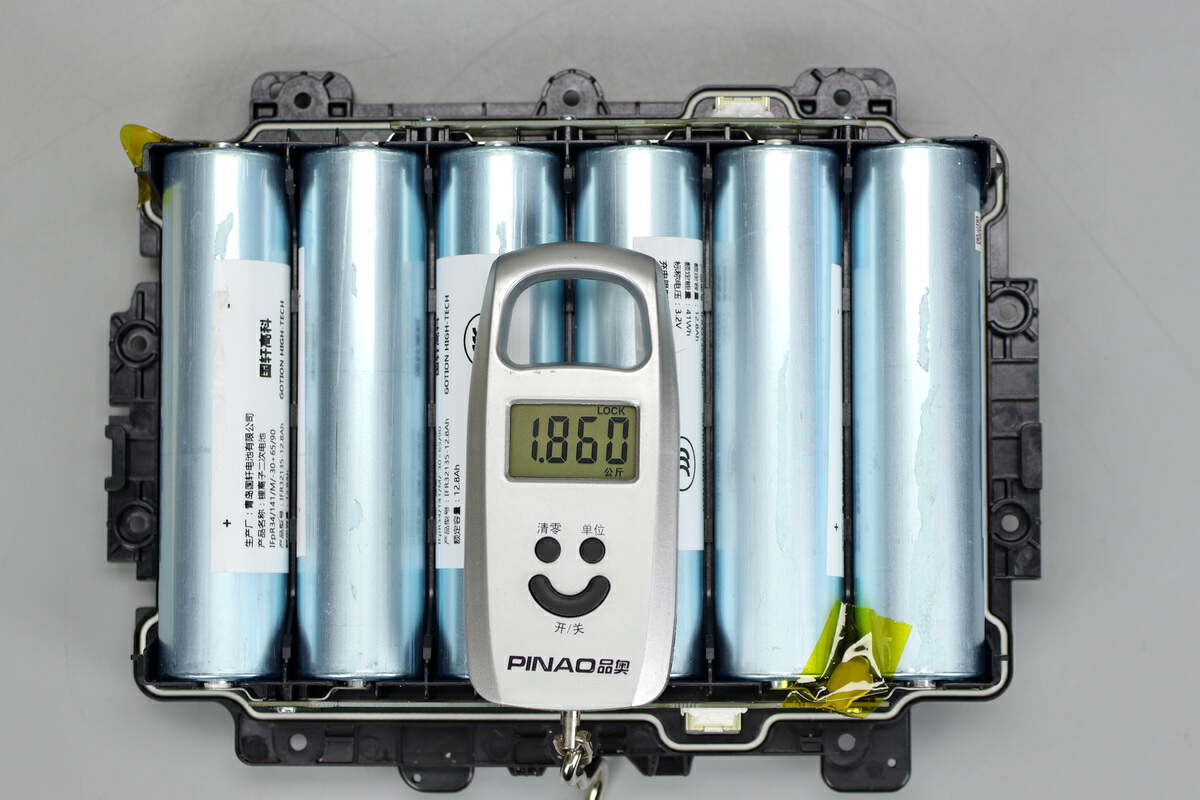
The weight of the battery pack is about 1.86 kg (4.1 pounds).
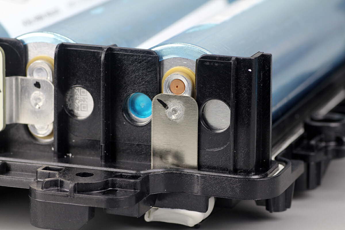
The positive and negative electrodes of the battery pack are connected and led out through nickel strip spot welding.
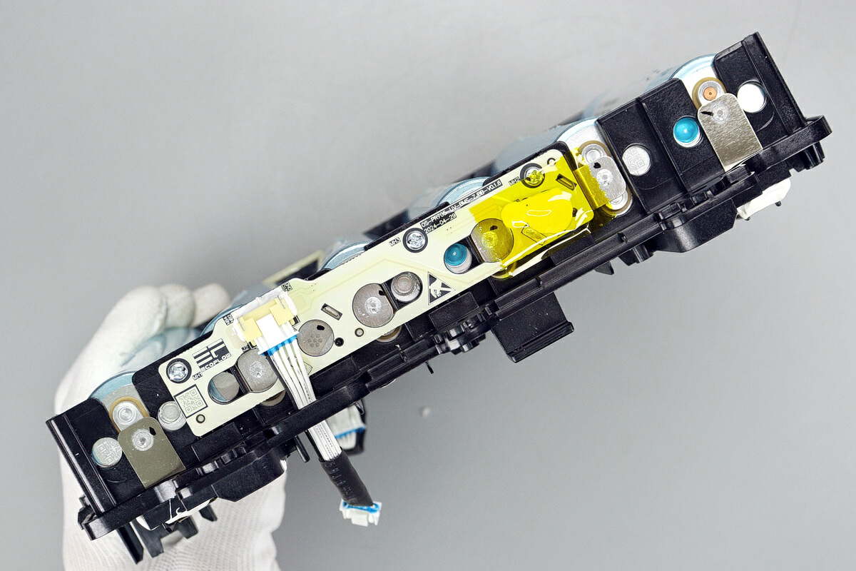
The battery nickel sheet is welded on the side of the battery pack, and a split voltage sampling wire is provided. The thermistor for detecting the battery temperature is glued and insulated with tape.
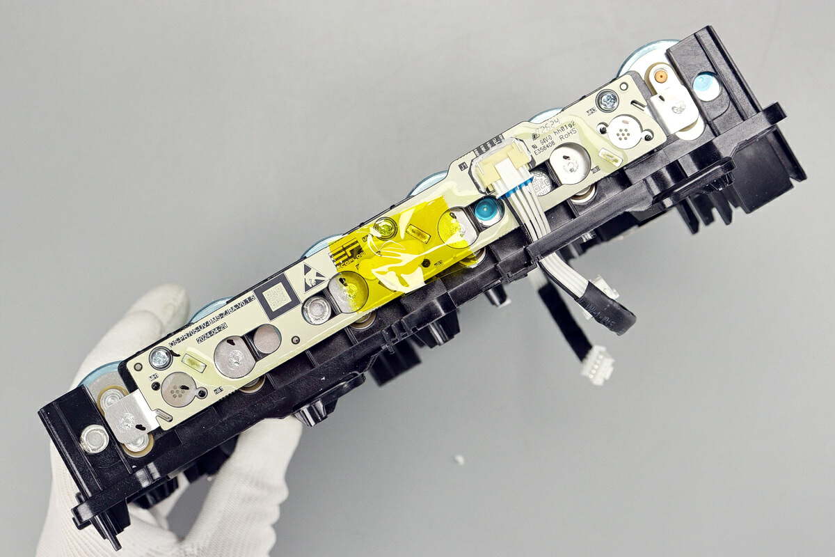
There is also a thermistor on the other side.
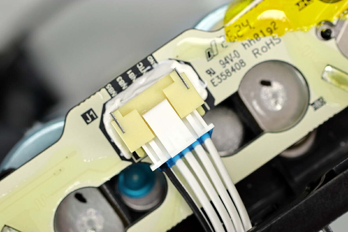
This is the socket for the wire used to detect the battery split voltage.
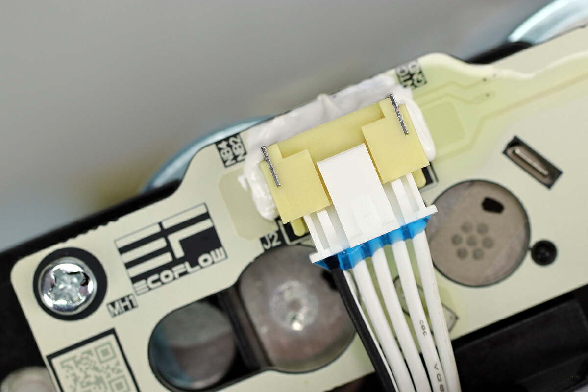
There is also a socket on the other side.
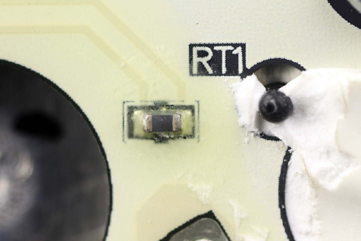
The thermistor is covered with glue and is used to detect the battery pack temperature.
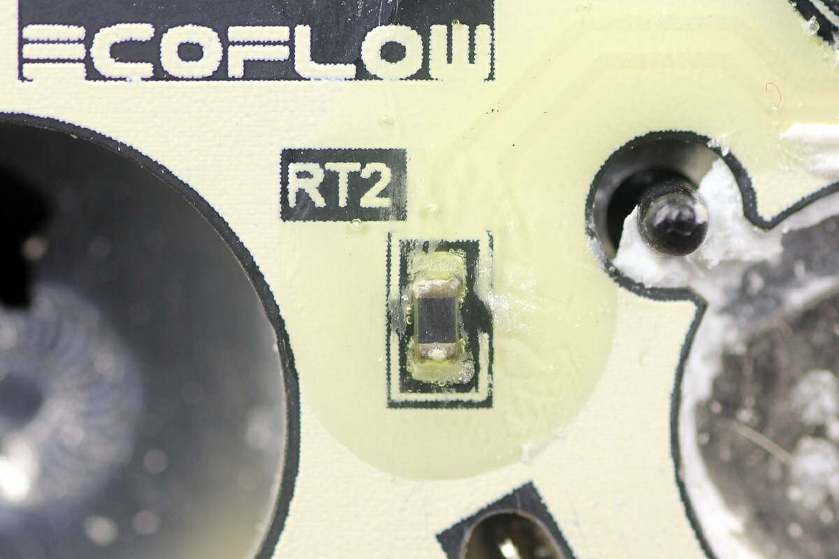
There is also a thermistor on the other side.
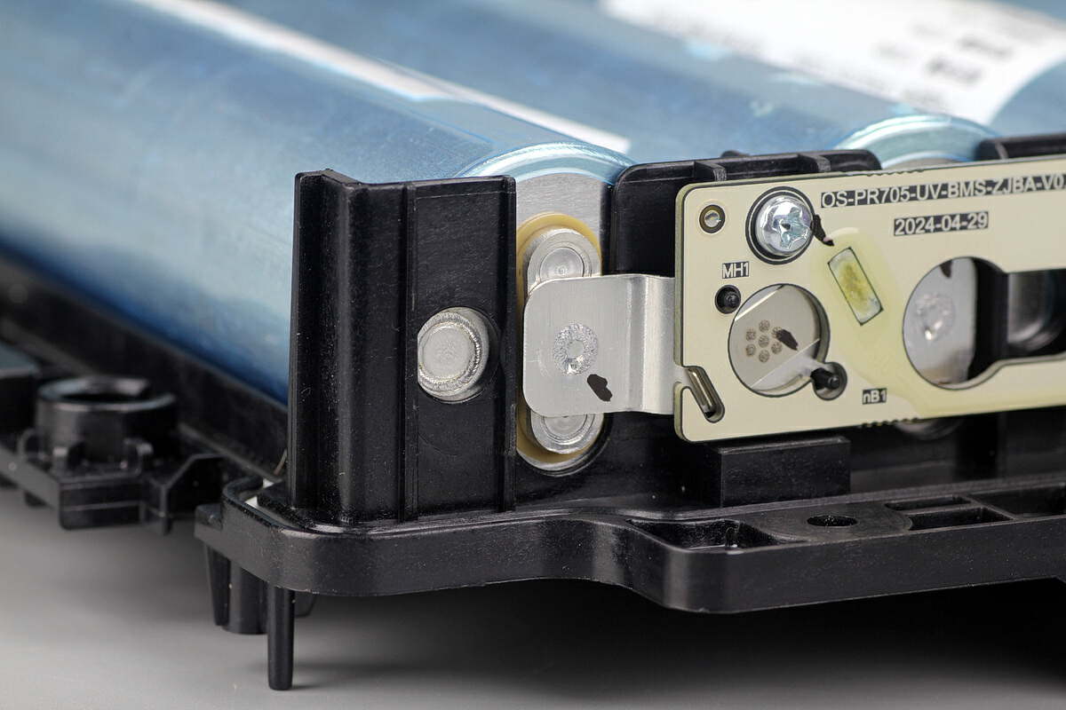
The cells are connected via nickel ribbon spot welding.
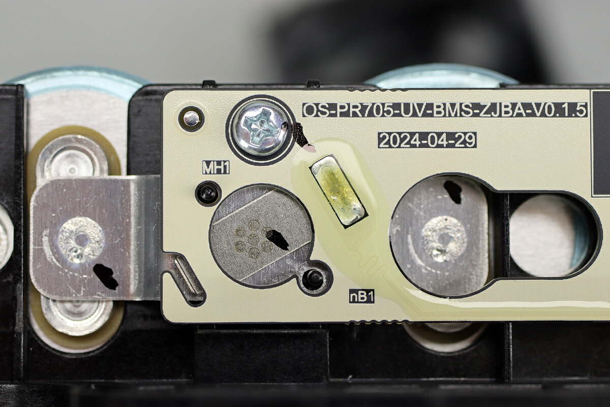
The small plates are fixed by screws and connected by spot welding.
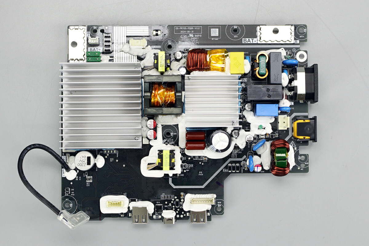
The front of the bidirectional inverter module has the positive and negative terminals of the battery pack and the fuse. There is a large heat sink on the left side to dissipate heat for the MOSFET. There is a transformer on the right side of the heat sink. There are heat sinks, filter inductors, filter capacitors, and relays for switching input and output on the right side of the transformer. There is an AC input interface and a DC input interface on the right side.
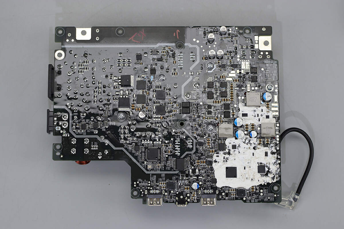
On the back are components such as a current detection chip, digital isolator, master control chip, battery protection chip, GaN power chip, GaN FET, etc.
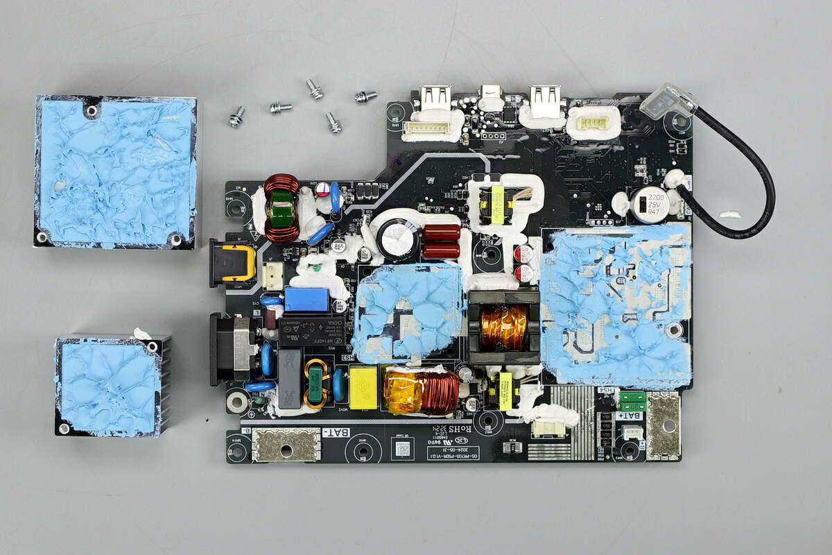
Unscrew the fixing screws of the heat sinks. The back of the heat sinks are coated with blue thermal gel.
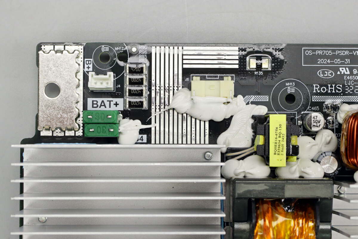
The battery input end has components such as a fan interface, fuse, battery cell voltage sampling socket, and current detection resistor.
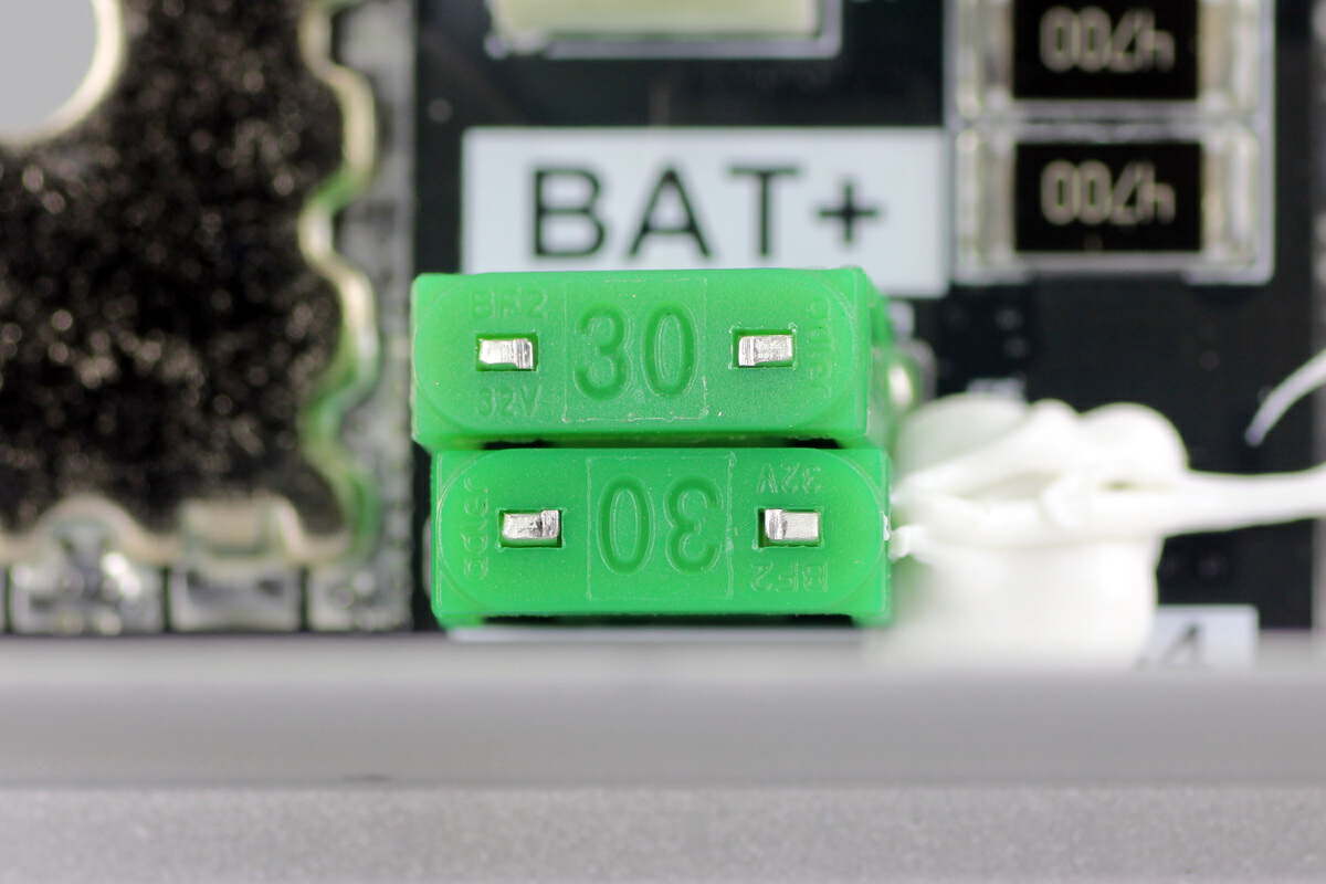
Two fuses are connected in parallel for overcurrent protection at the battery end. 30A.
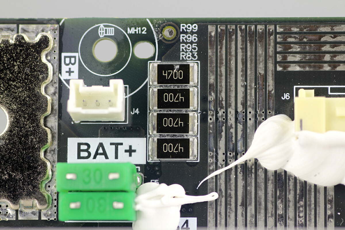
These four resistors are connected in parallel. 470Ω.
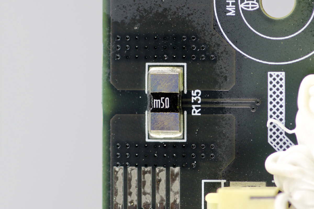
The sampling resistor is used to detect the battery current. 0.5mΩ.
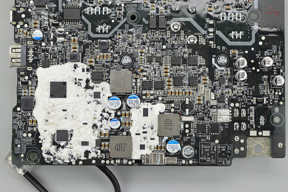
On the left side of the low-voltage circuit are the master control chip and battery protection chip. On the right side of the master control chip is the current sampling chip and protocol chip. In the middle are the synchronous buck-boost converter and synchronous buck converter, as well as the corresponding SMD inductor.
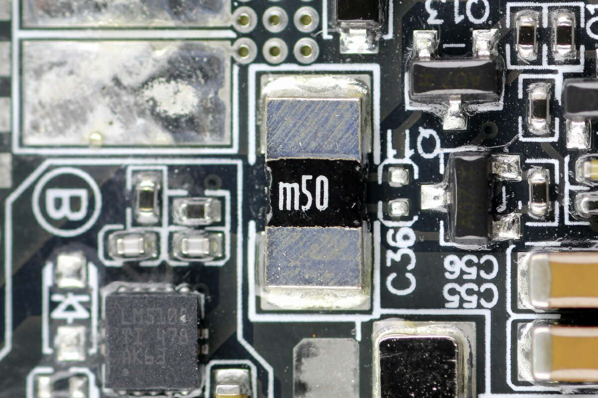
The sampling resistor is used for positive current detection. 0.5mΩ.
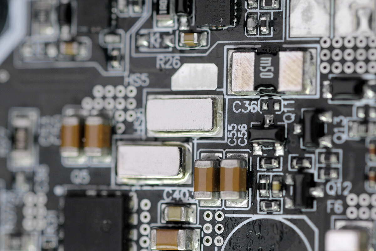
The PCB increases current carrying capacity by soldering copper sheets.
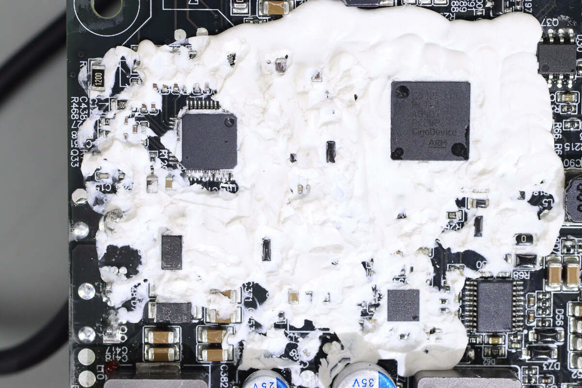
This is the battery protection chip and MCU.
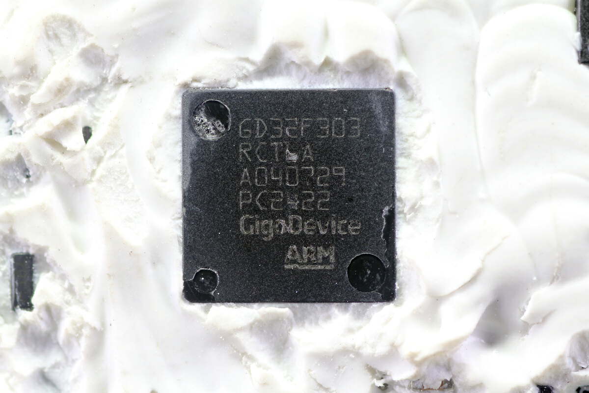
The MCU is from GigaDevice and adopts LQFP64 package. It has a main frequency of 120MHz, a built-in Cortex-M4 core, 256KB FLASH, and 48KB SRAM, and supports PWM signal output. Model is GD32F303RCT6A.
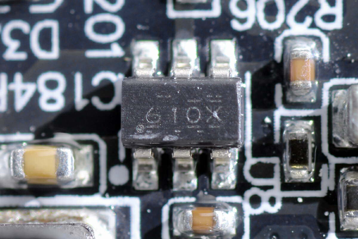
The synchronous buck chip marked with 610X is from TI and adopts SOT23-6 package. It has a 4-65V input voltage range, an output current of 1A, and a switching frequency of 400kHz. Model is LMR51610X.
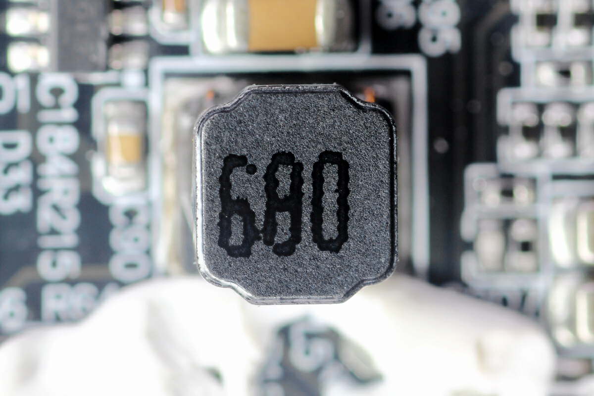
This is the buck inductor. 68μH.
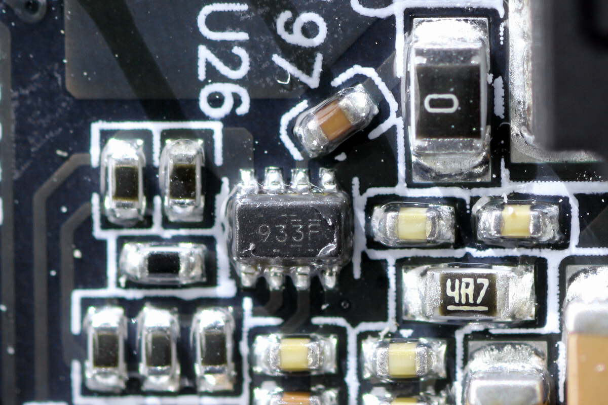
The synchronous buck chip marked with 933F is from TI and adopts SOT583 package. It supports 30V input voltage and 22V output voltage, with a continuous output current of 3A. Model is TPS62933F.

This is the buck inductor. 10μH.
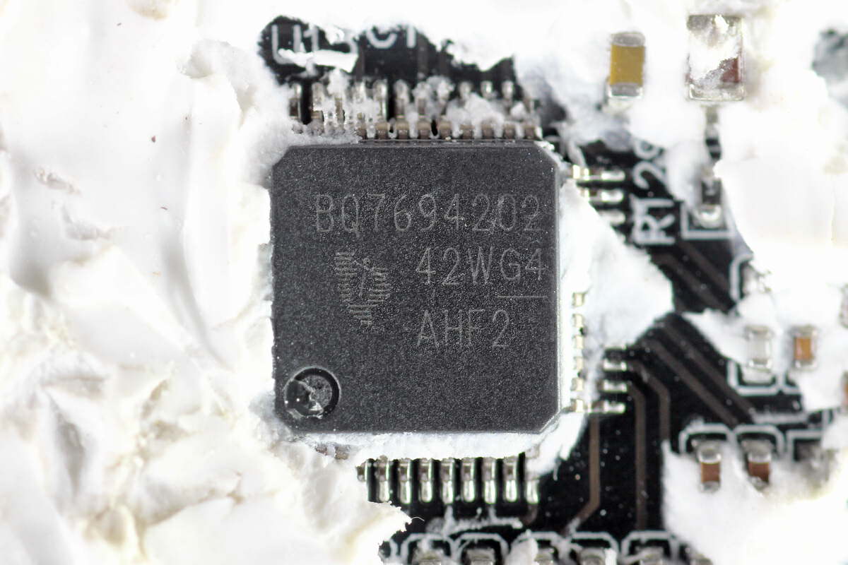
The battery protection chip is from TI and adopts TQFP48 package. It supports 3-10 series lithium battery and lithium iron phosphate battery applications. It integrates the NMOS driver, dual-channel programmable LDO, and I2C communication interface, integrates two independent ADCs, and supports voltage and current synchronous sampling. Model is BQ7694202.
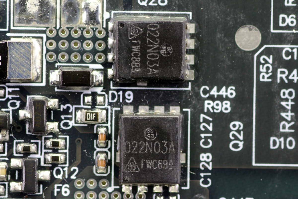
The two MOSFETs for power supply control are from CR MICRO and adopt PDFN5*6 package. 30V 1.6mΩ. Model is HGQ022N03A.
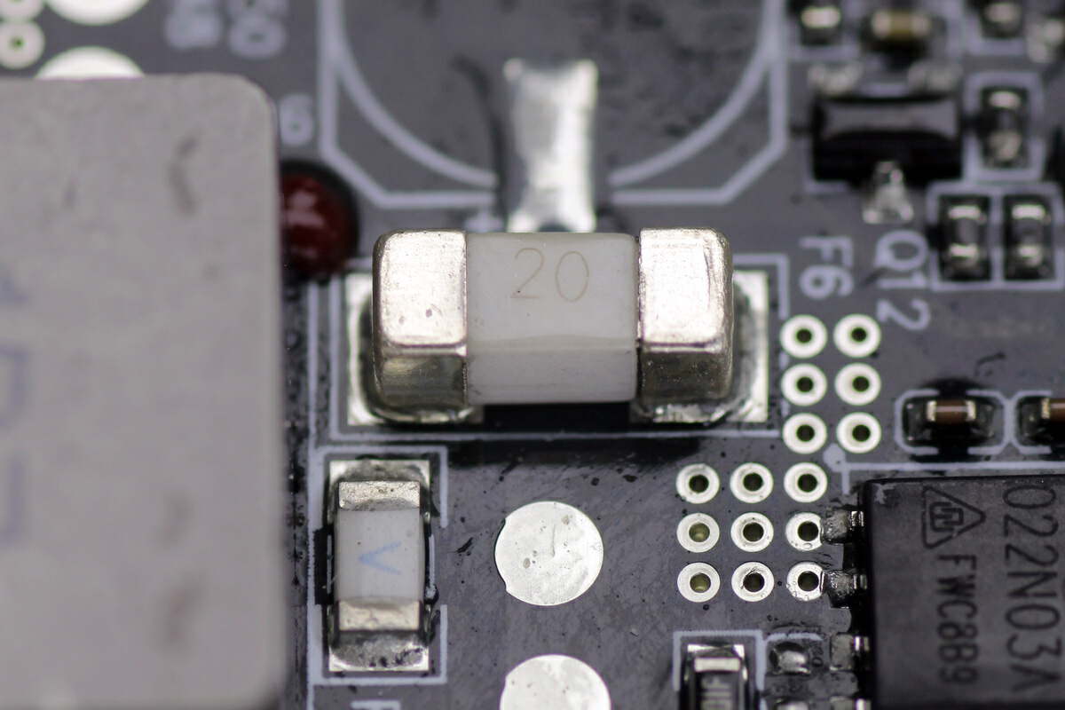
This is an SMD fuse. 20A.
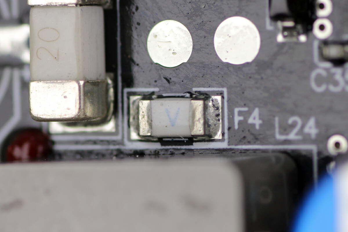
This is an SMD fuse marked with V.
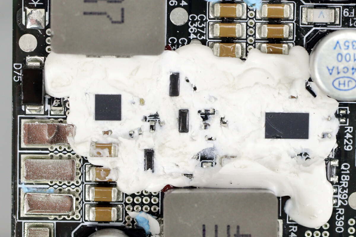
This is the synchronous buck converter and the synchronous buck-boost converter.
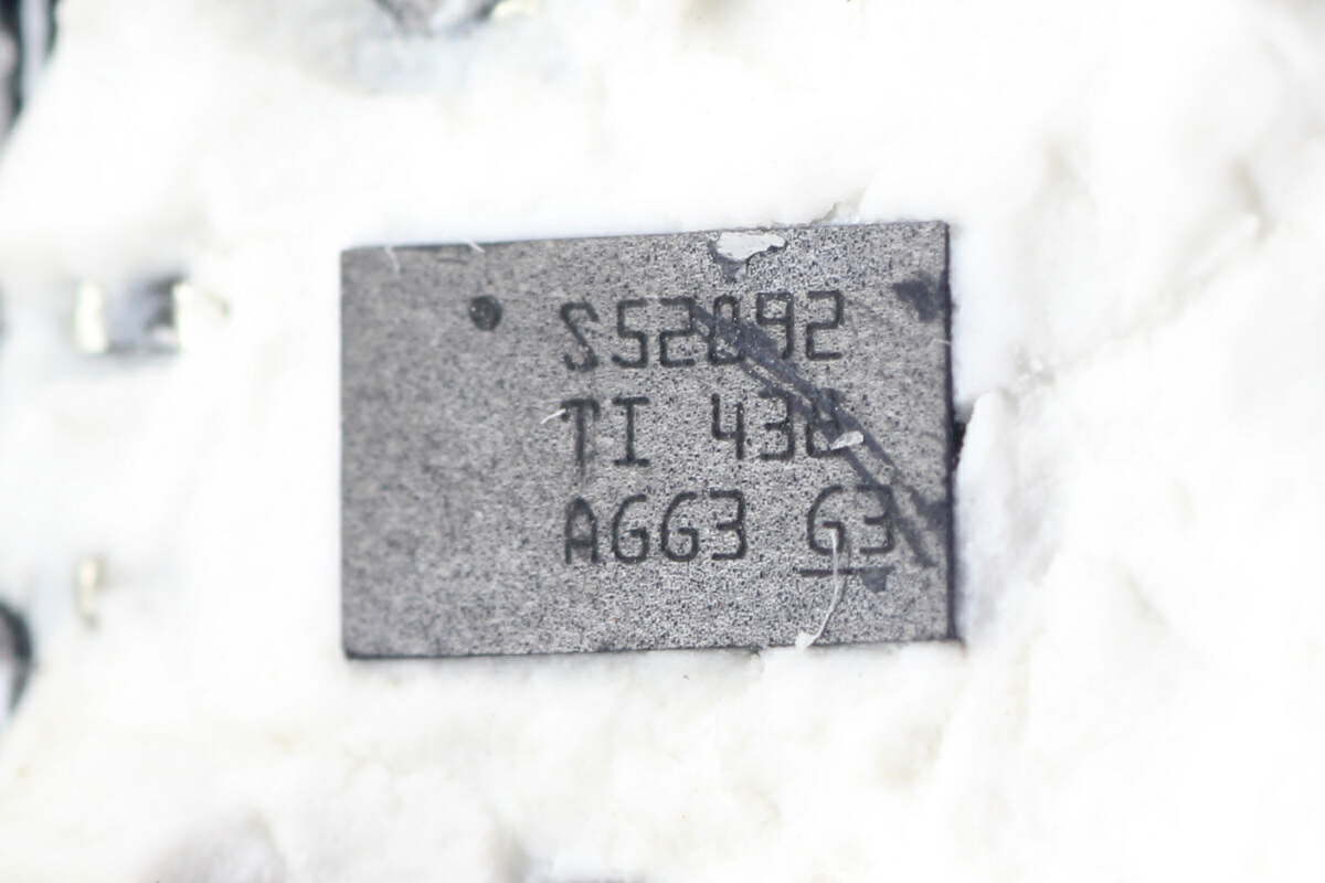
The synchronous buck-boost chip marked with S52892 is from TI and adopts VQFN-21 package. It has an integrated MOSFET, supports 36V input voltage and 22V output voltage, and supports 200kHz-2.2MHz switching frequency. Model is TPS552892.
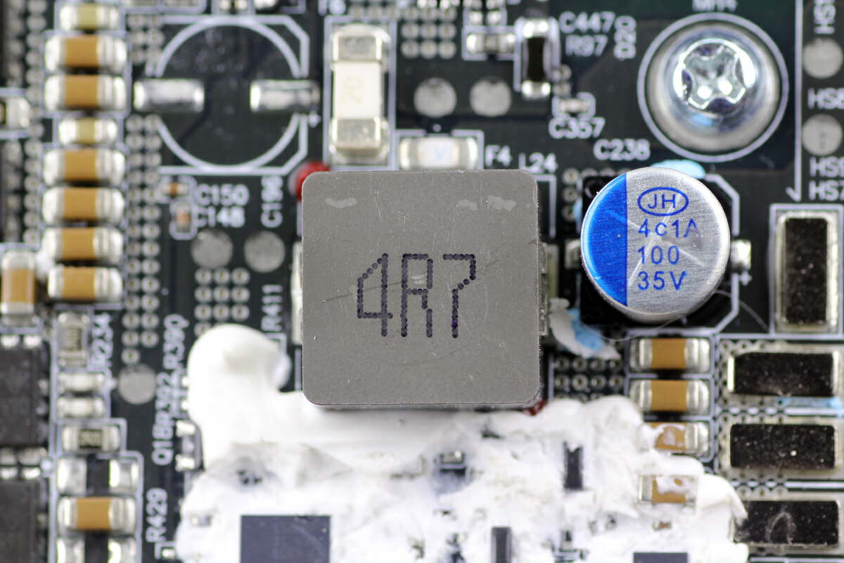
The alloy inductor is used for buck-boost voltage conversion. 4.7μH.
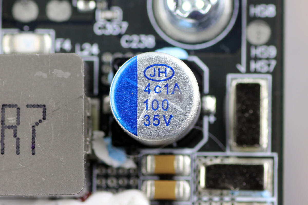
The filter capacitor is from Jianghai. 100μF 35V.
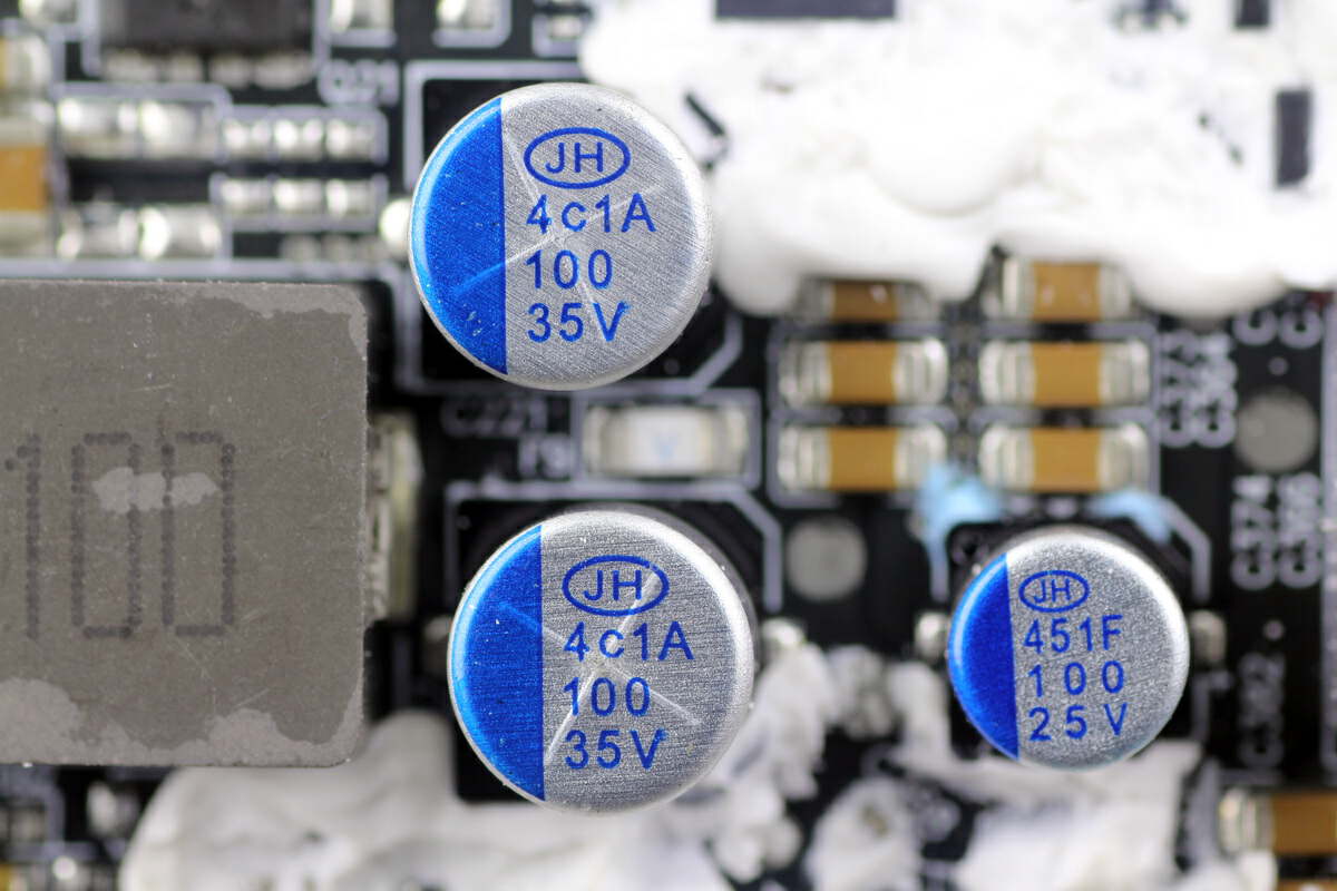
This filter capacitor has the same specifications as the previous one.
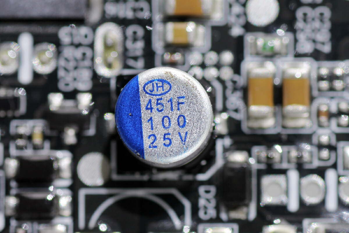
The specification of this filter capacitor is 100μF 25V.
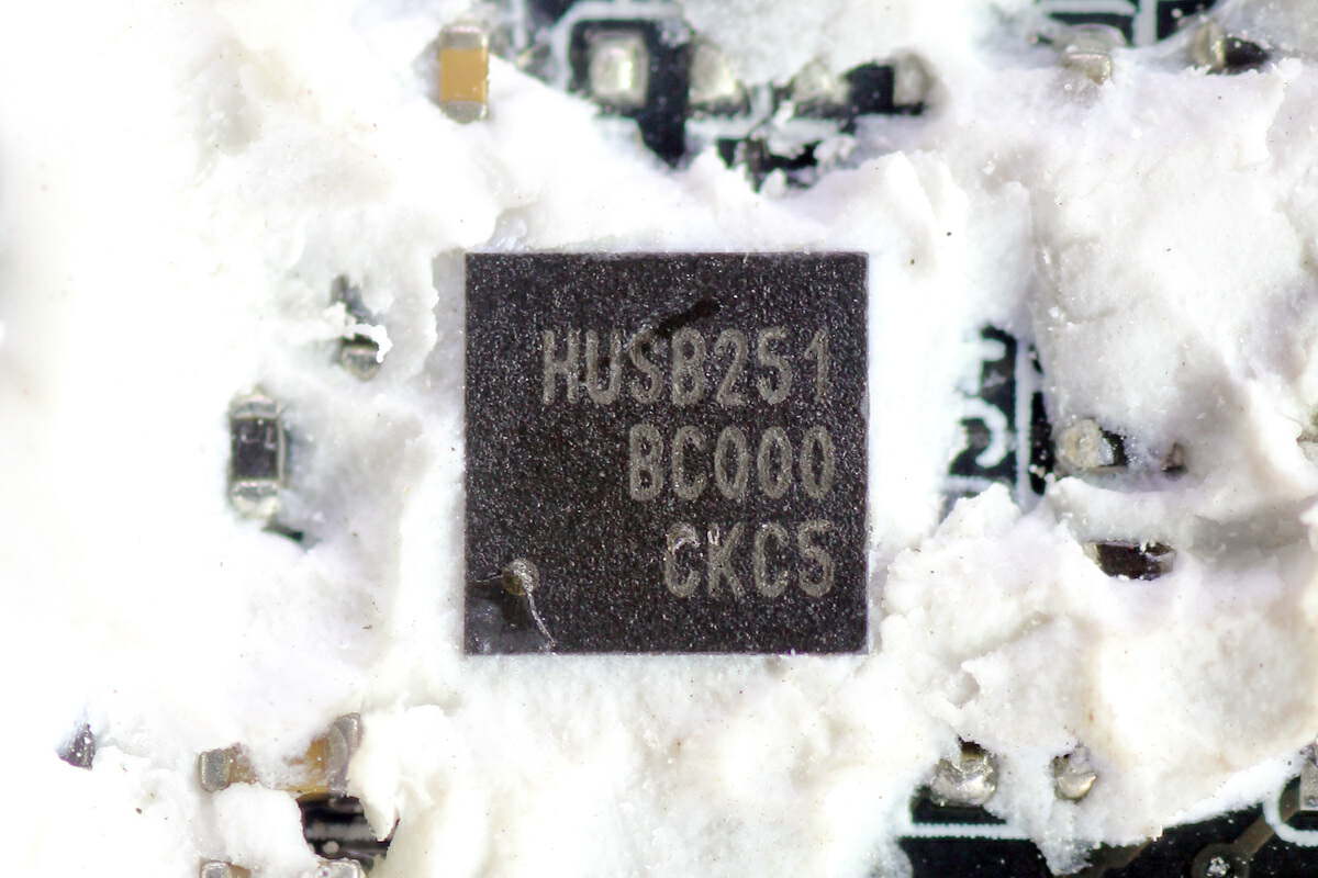
The USB-C protocol chip is from Hynetek and adopts QFN24 package. It is a PD protocol chip that supports USB Type-C DRP. It supports PPS PDO and EPR PDO, supports QC2.0, QC3.0, AFC, FCP, and UFCS fast charging modes, and has very good fast charging compatibility. Model is HUSB251.
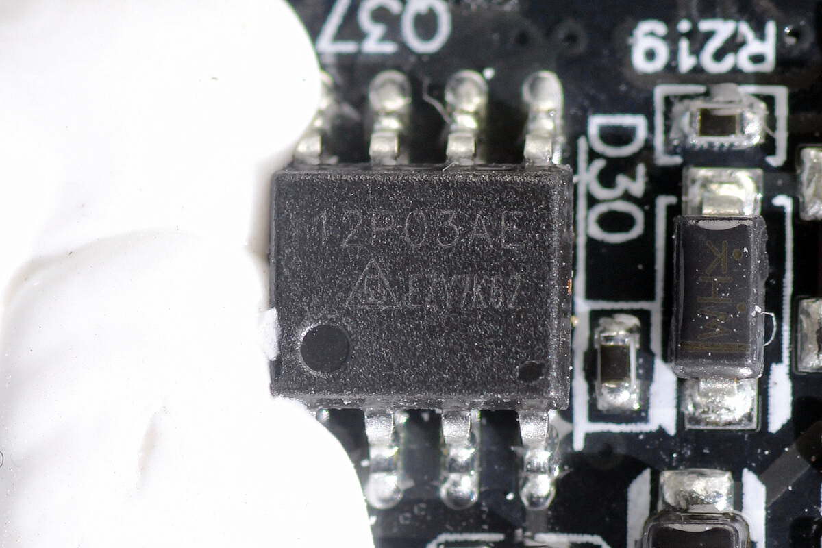
The MOSFET is from CR MICRO and adopts SOP-8 package. PMOS, withstand voltage -30V, conduction resistance 11mΩ. Model is CS12P03AE.
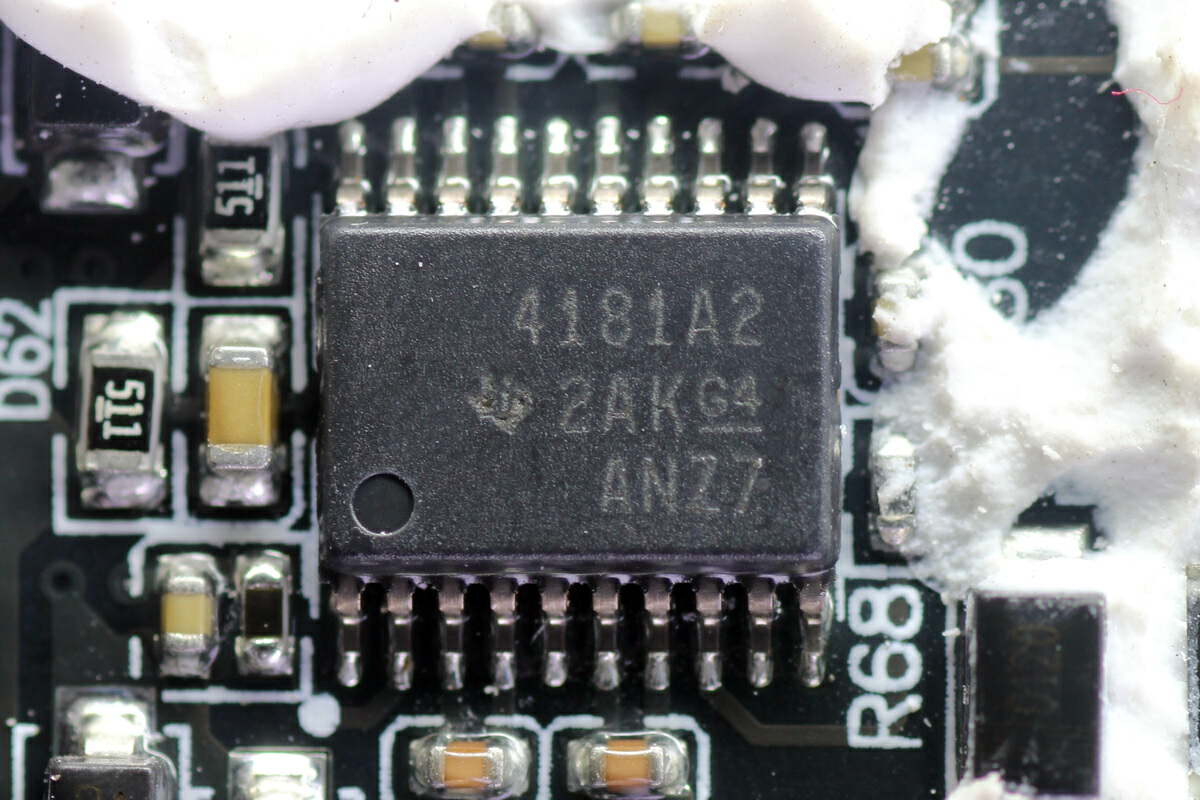
The current detection chip marked with 4181A2 is from TI and adopts TSSOP-20 package. It is a bidirectional low-side and high-side voltage output current detection amplifier. It has four built-in detection channels for USB-C, USB-A interface, and DC output interface current detection. Model is INA4181A2.
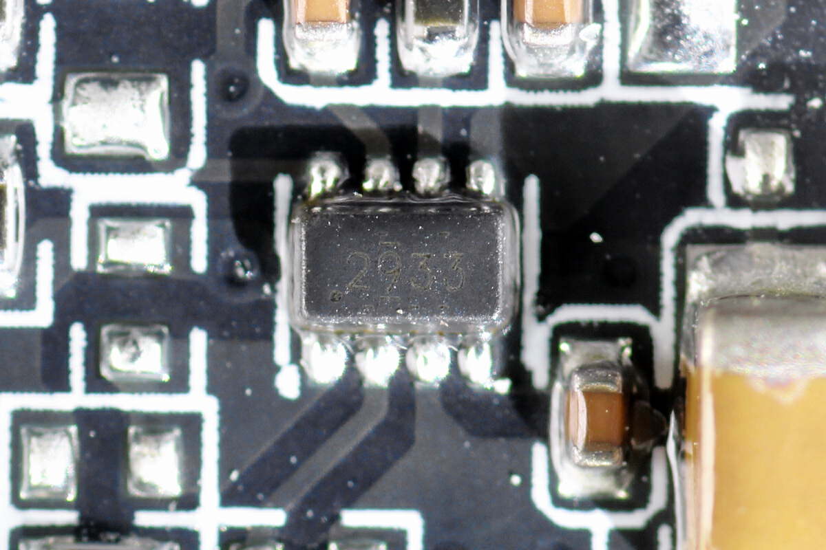
The synchronous buck chip marked with 2933 for the USB-A is from TI and adopts SOT583 package. It is a synchronous buck converter that supports 30V input voltage, 3A output current, and 22V output voltage. Model is TPS62933.
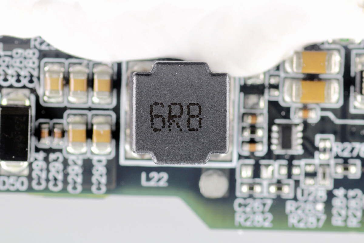
This is the buck inductor. 6.8μH.
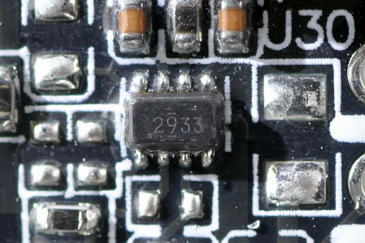
This is another synchronous buck chip. Model is TPS62933.
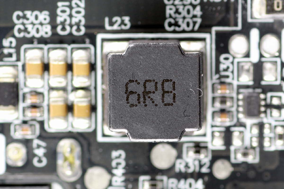
This is the buck inductor. 6.8μH.
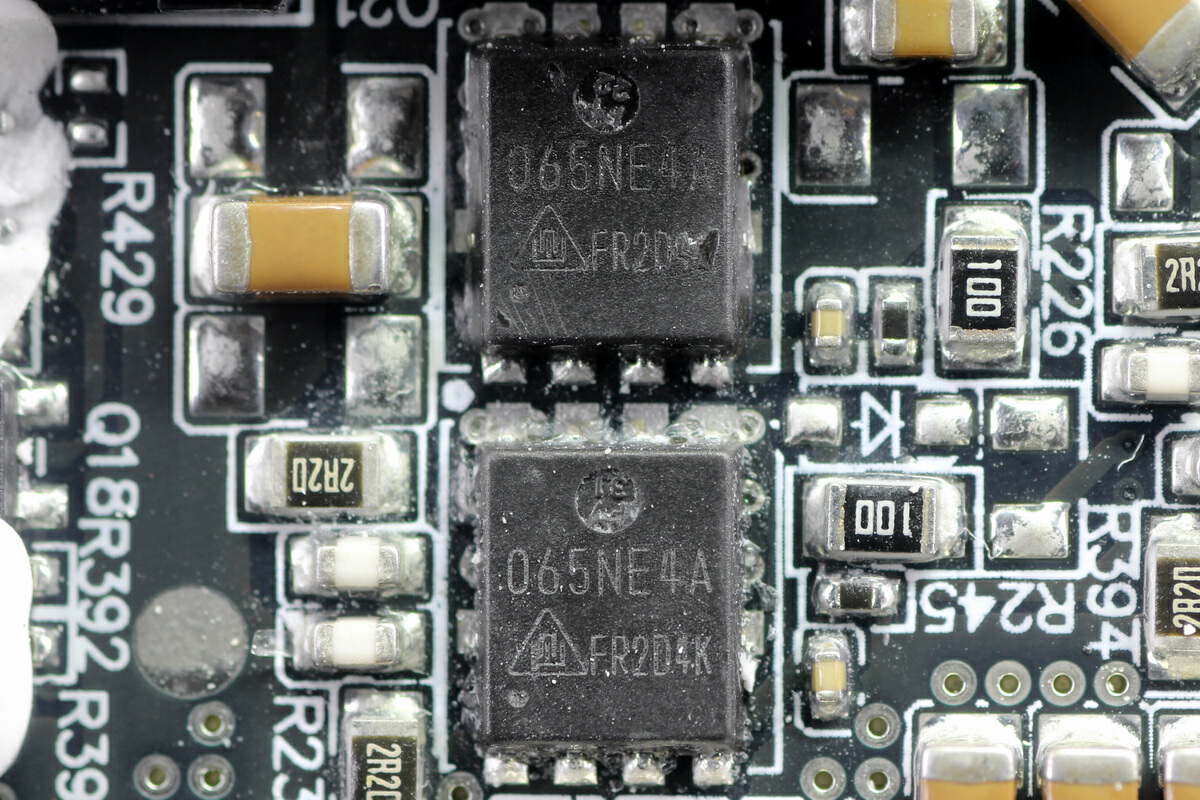
These two MOSFETs are from CR MICRO and adopt PDFN5*6 package. 40V 5.2mΩ. Model is HGQ065NE4A.
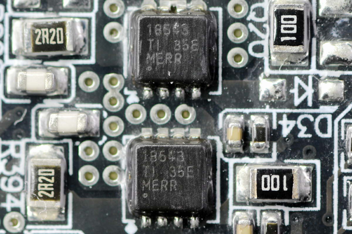
These two MOSFETs marked with 18543 are from TI and adopt SON3.3*3.3 package. 60V 8.1mΩ. Model is CSD18543Q3A.
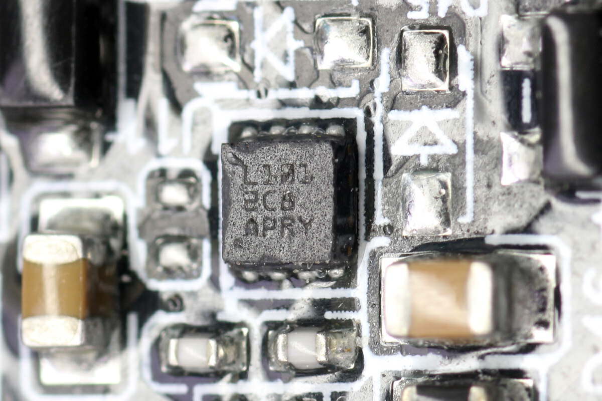
The half-bridge driver marked with L101 is from TI and adopts WSON8 package. It supports dual NMOS drivers with 0.5A source current and 0.8A sink current capability. Model is LM2101.
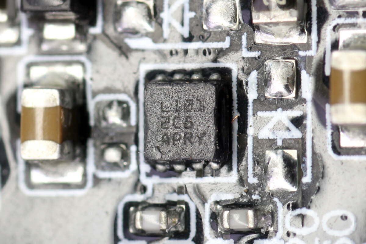
The other drive has the same model.
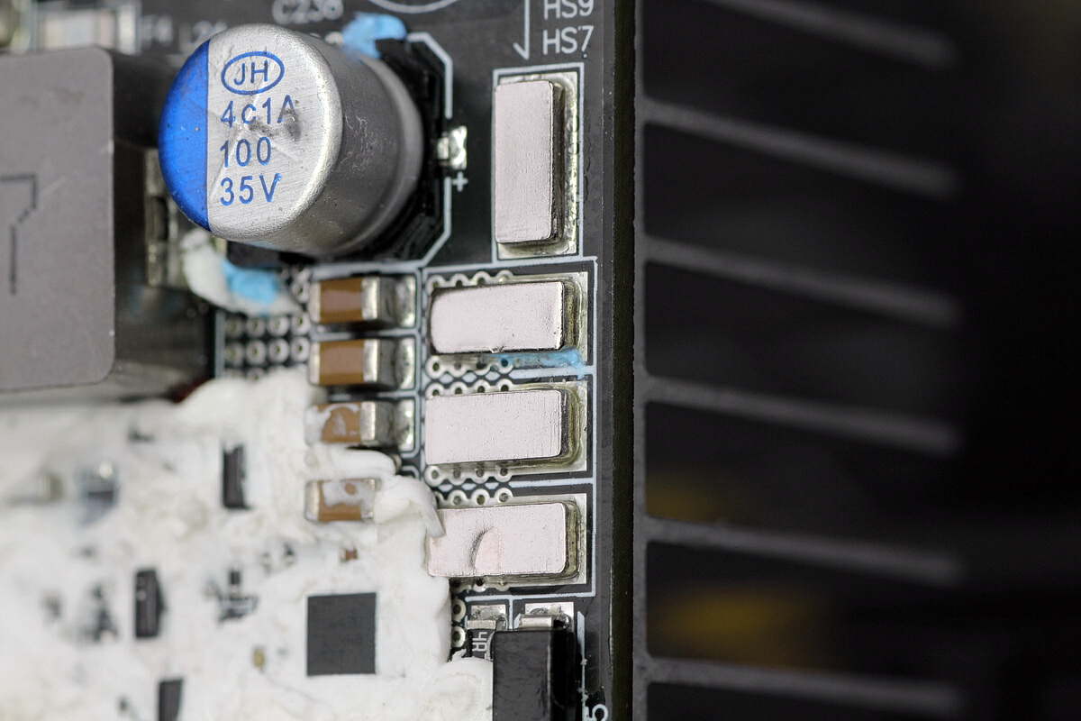
This is the copper strip that enhances current carrying.
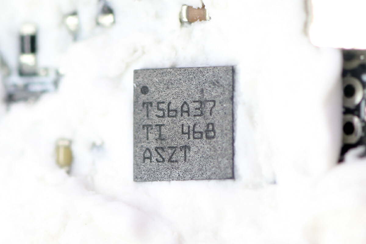
The synchronous buck chip marked with T56A37 is from TI and adopts QFN-10 package. It supports 28V input voltage and 13V output voltage. It has an internal integrated MOSFET, supports 10A output current, a switching frequency of 500kHz, has a normal power status indication, and supports overvoltage, undervoltage protection, overcurrent protection, and overheating protection. Model is TPS56A37.
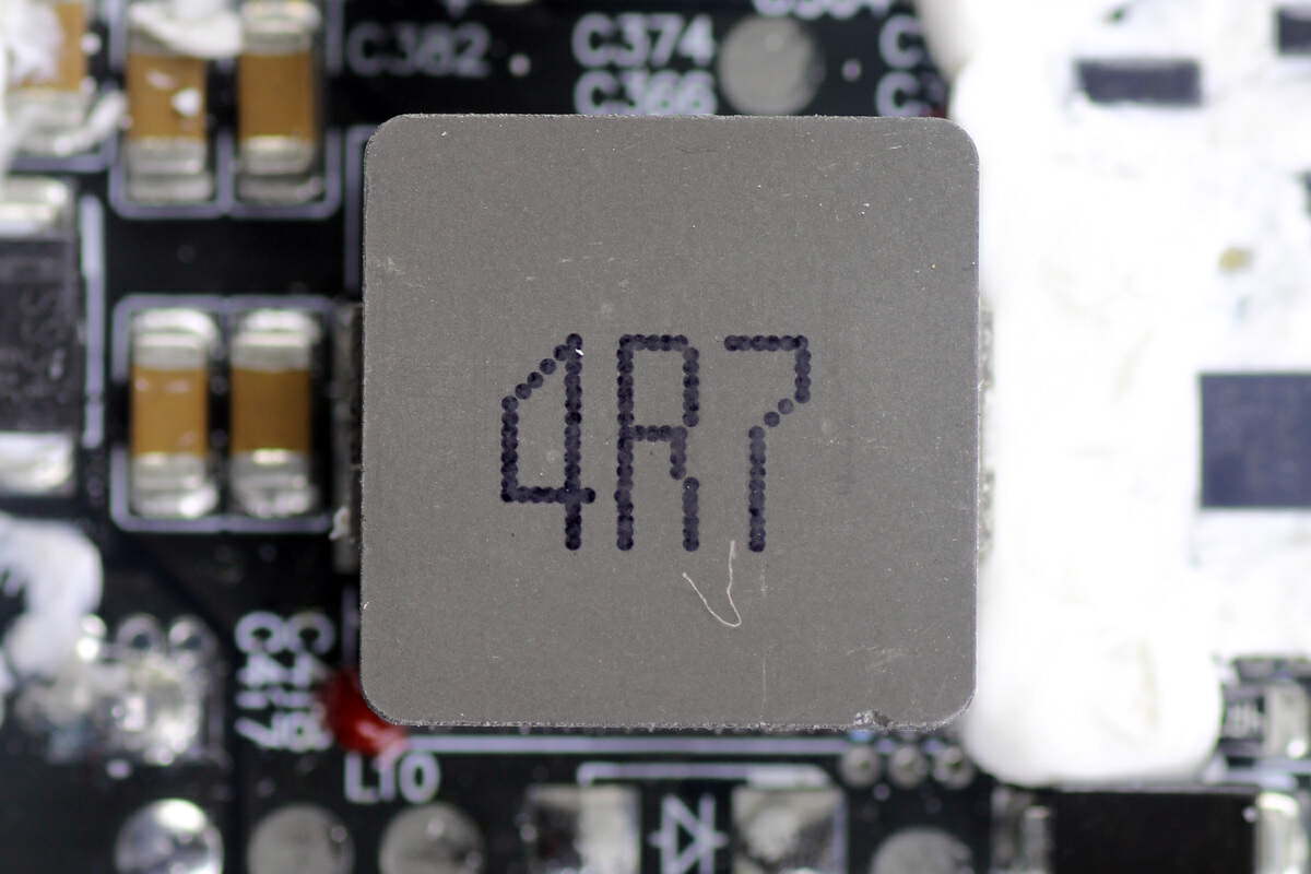
This is the buck inductor. 4.7μH.
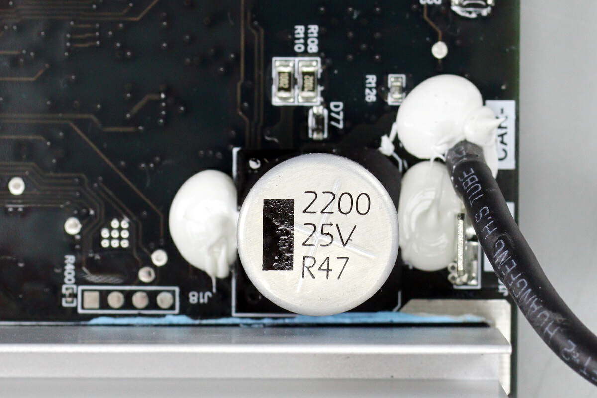
This is the output filter capacitor. 2200μF 25V.
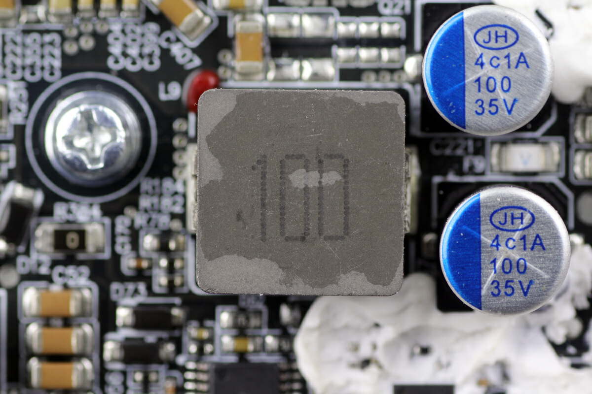
This is an alloy inductor. 10μH.
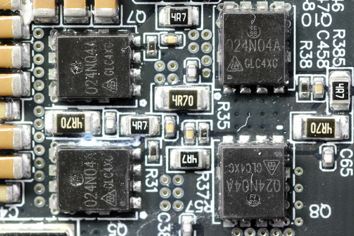
The MOSFET used for inverter boost and synchronous rectification is from CR MICRO and adopts PDFN5*6 package. 40V 1.6mΩ. Model is HGQ024N04A.
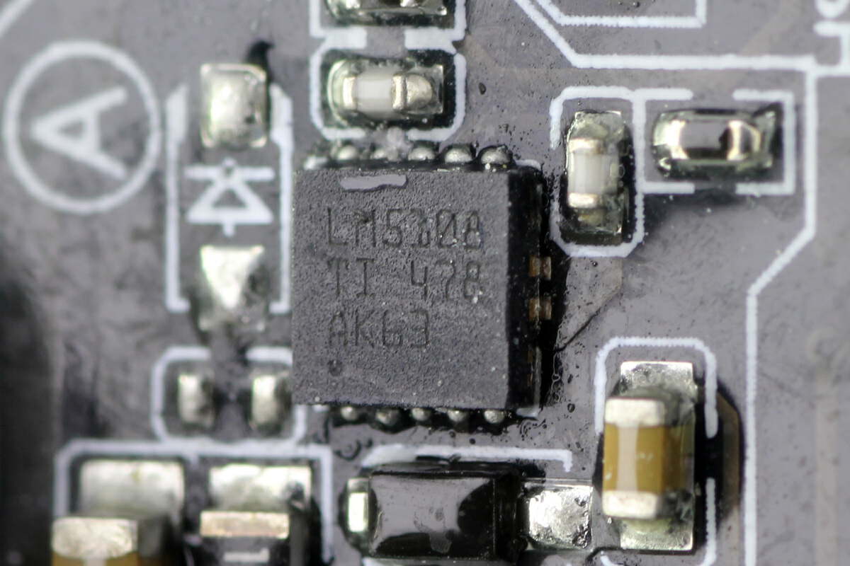
The low-voltage MOSFET driver is from TI and adopts SON10 package. It has a voltage resistance of 100V, 2.6A sink current and 1.6A source current output, and it has interlock protection and supports enable control. Model is LM5108.
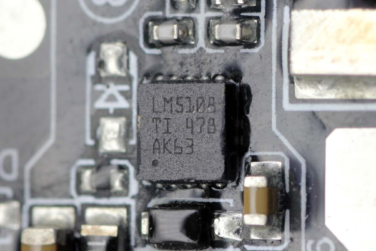
Another drive has the same model.
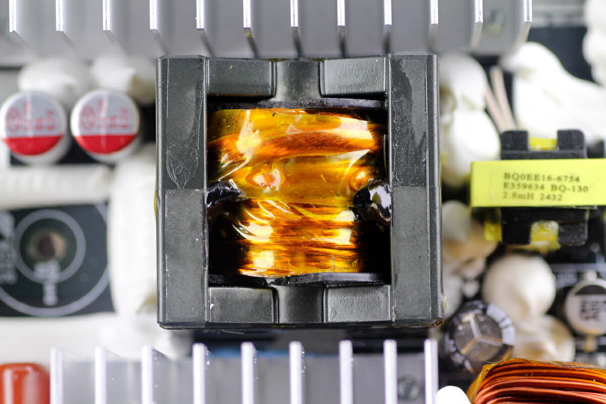
The primary and secondary of the step-up transformer are both wound with Litz wire to reduce losses.
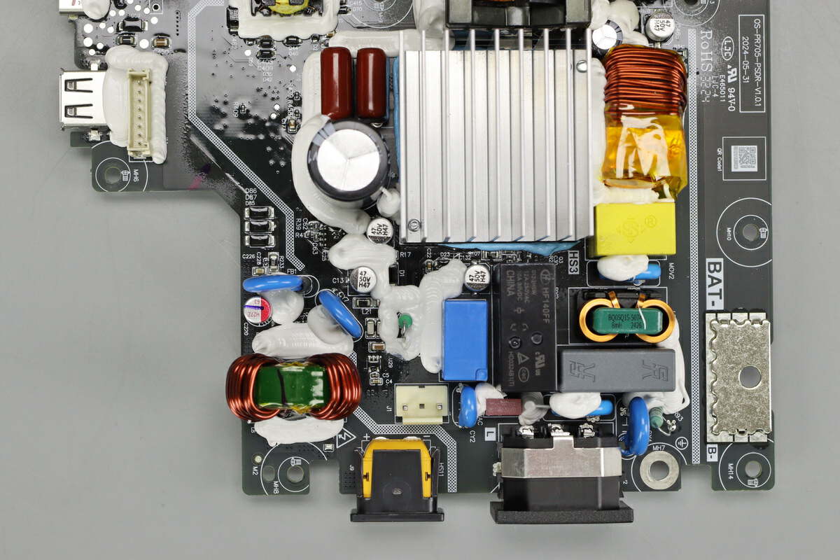
There are resonant capacitor and filter capacitor on the left side of the heat sink. There are filter inductor, common mode choke, and switching relay on the right side. There are DC input and AC input sockets at the bottom.
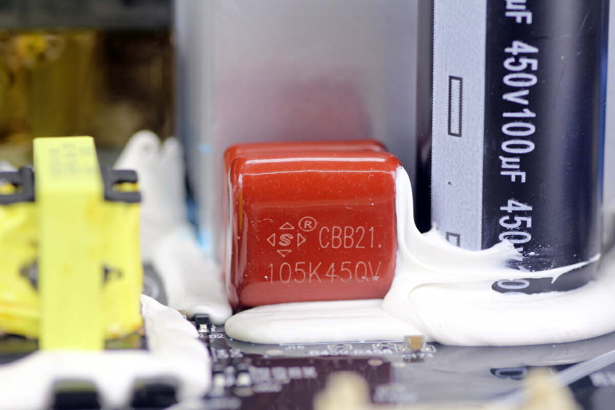
These two film capacitors are from STE. 1μF 450V.
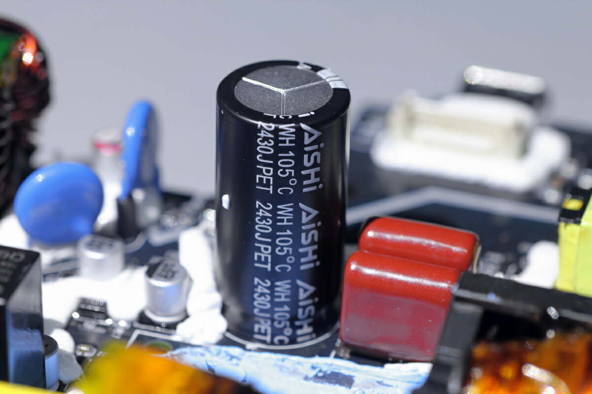
The high-voltage filter capacitor is from AiSHi, which is a WH series electrolytic capacitor. 450V100μF.
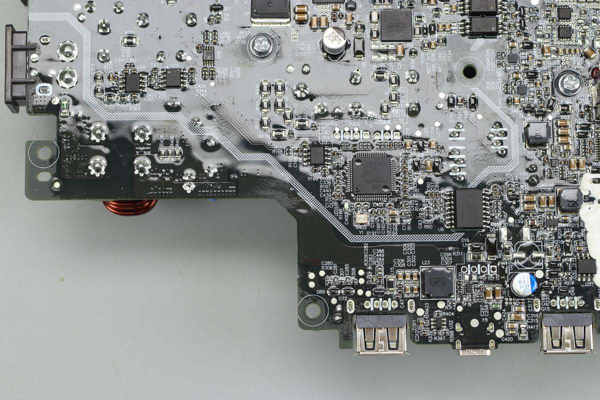
The high-voltage side of the bidirectional inverter module is equipped with a master control chip and a digital isolator.
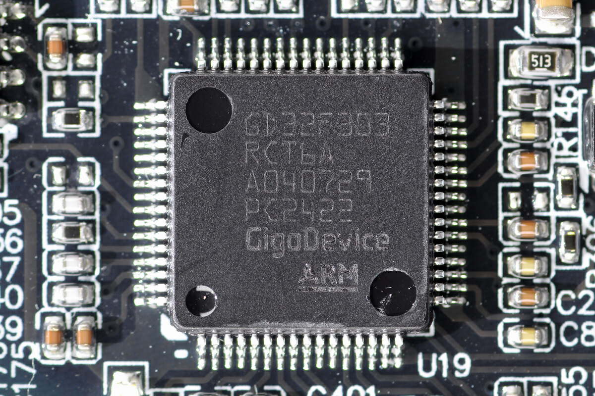
Another MCU for output modulation and PFC control is from GigaDevice. Model is GD32F303RCT6A.
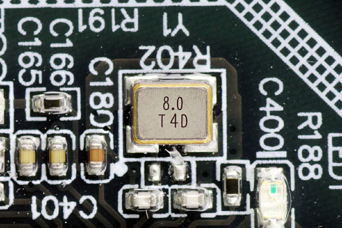
This is the clock crystal. 8.000MHz.
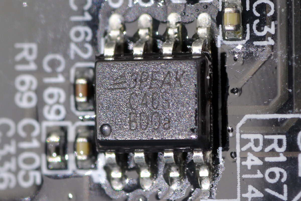
The dual voltage comparator marked with C46S is from 3PEAK and adopts SOIC8 package. It supports 1.8-5.5V operating voltage. Model is LMV393TP.
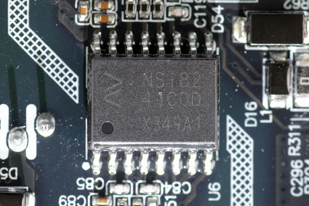
The digital isolator is from NOVOSENSE and adopts SOW16 package. It has three forward channels and one reverse channel, supporting DC-150Mbps data rate. Model is NSi8241C.
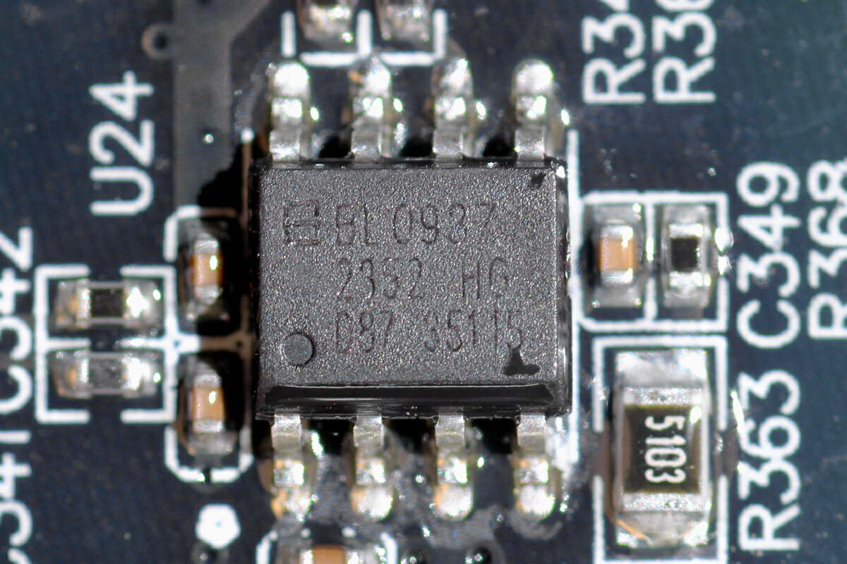
The single-phase energy metering chip for collecting voltage and current parameters of inverter output is from Belling and adopts SOP8 package. Model is BL0937.
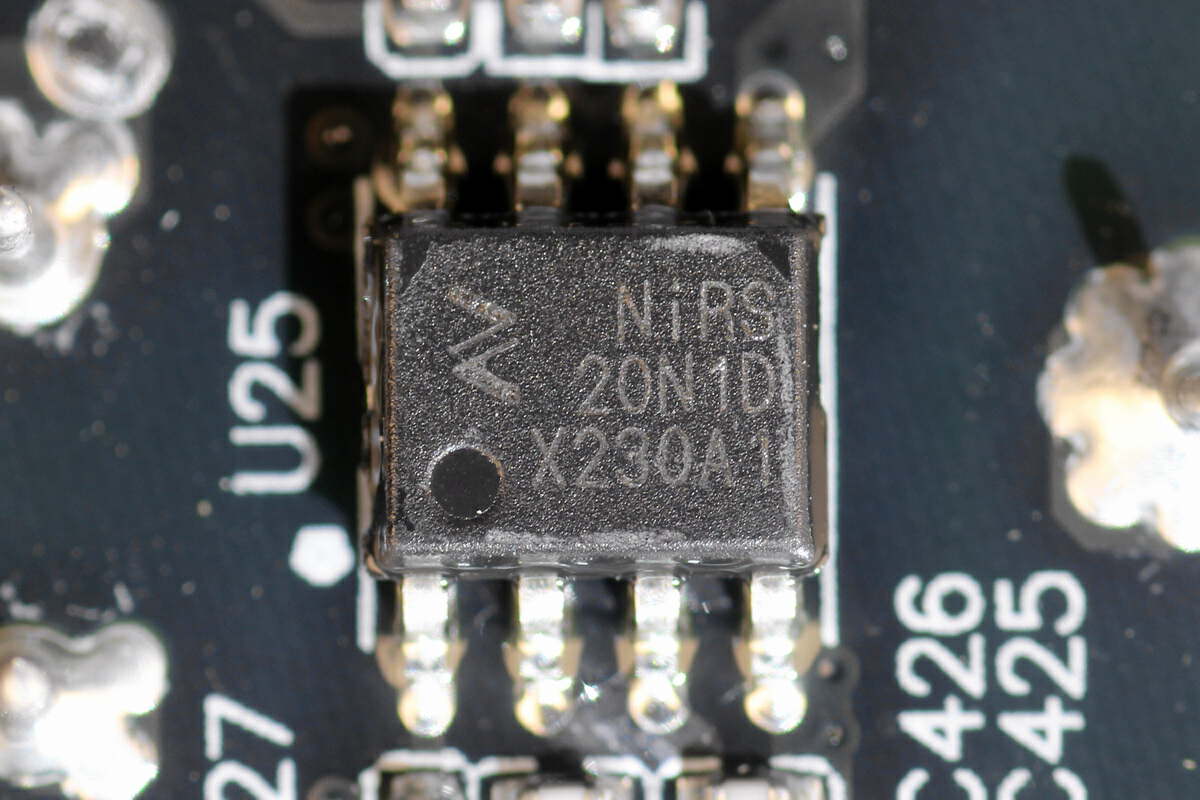
The digital Isolation Chip is from NOVOSENSE and adopts SOIC-8 package. It supports DC-500kbps data rate. Model is NIRS20N.
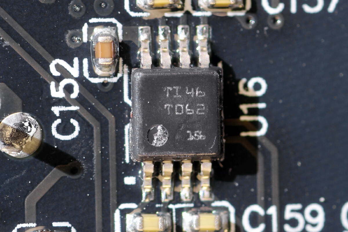
The Op-Amp marked with T062 is from TI and adopts VSSOP package. It is a rail-to-rail input and output dual op-amp that supports -40~125℃ operating temperature. Model is TLV9062.
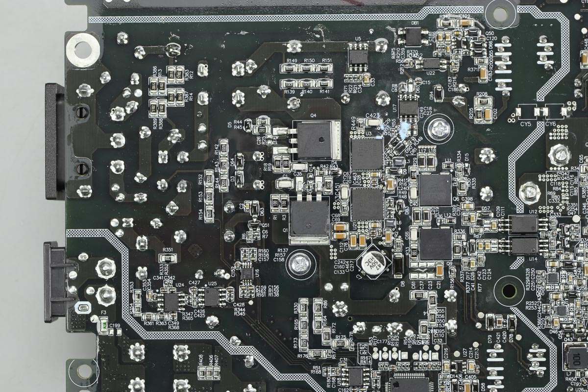
This is the IGBT and GaN power chip and GaN FET for output modulation.
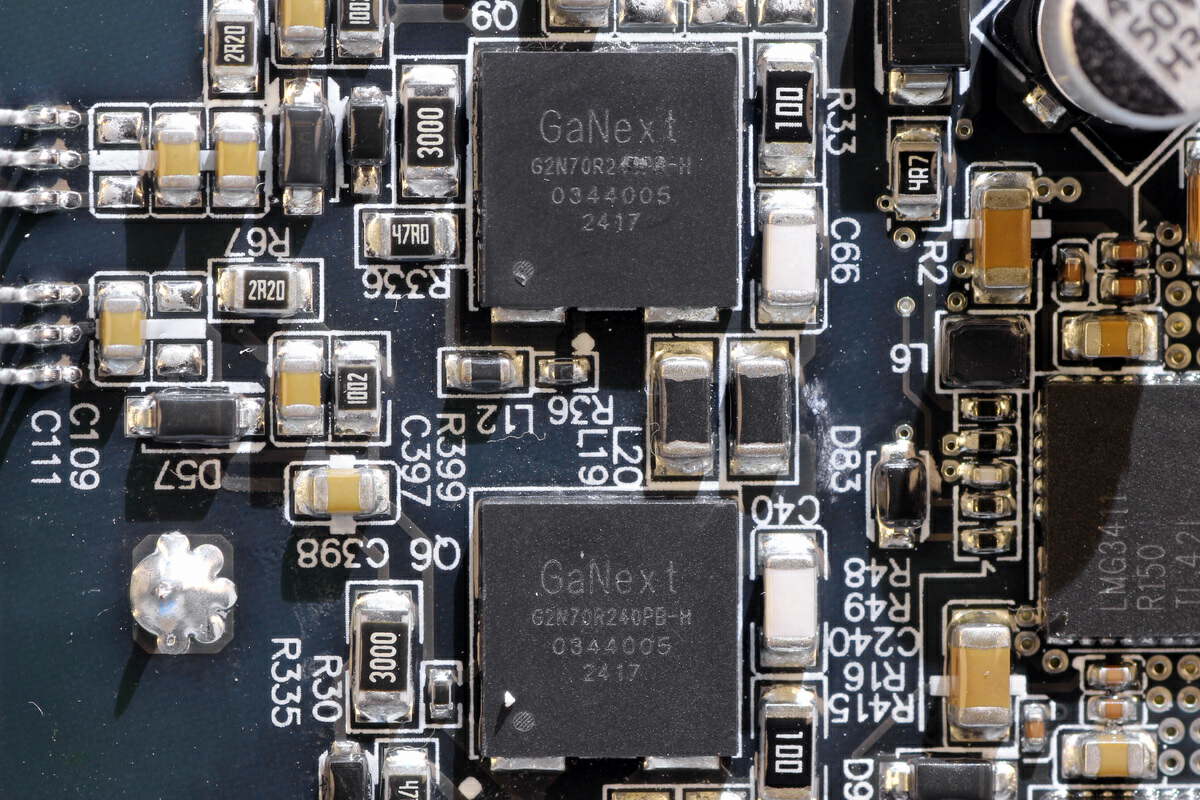
These two GaN FETs are from GaNext and adopt PQFN8*8 package. It is suitable for soft switching applications such as QR or ACF flyback topology, totem pole PFC, inverter and LLC. 700V 240mΩ. Model is G2N70R240PB-H.
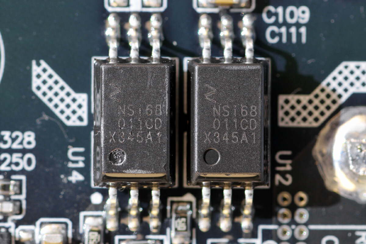
The isolation driver chip is from NOVOSENSE and adopts SOW6 package. It supports 1.5A/-2A drive current, is compatible with mainstream optically coupled gate drivers, has shorter propagation delay, higher ambient temperature, and higher reliability. Model is NSi68011C.
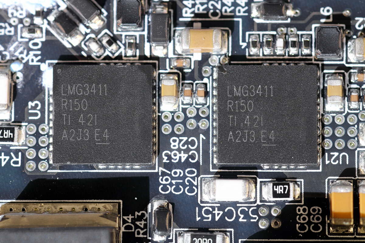
These two GaN FETs are from TI and adopt 8x8mm QFN package. It integrates driver and protection functions internally and has superior system performance compared to independent GaN FETs. It has a built-in 600V withstand voltage, 150mΩ conduction resistance GaN FET. The driver supports 12V supply voltage, the slew rate supports user adjustment, and has cycle-by-cycle overcurrent protection, overtemperature protection, and under-voltage lockout protection, and has a fault status signal output. Model is LMG3411R150.
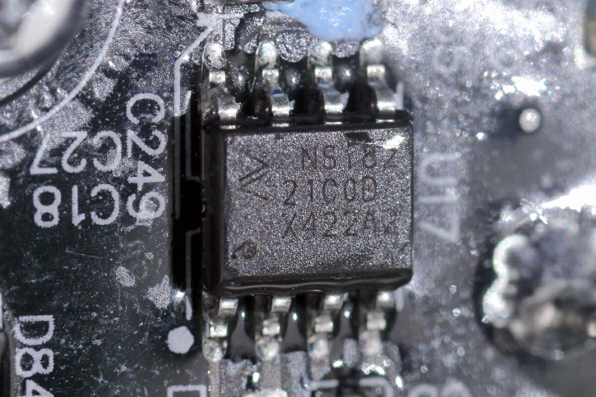
The digital isolator is from NOVOSENSE. Model is NSi8221C.
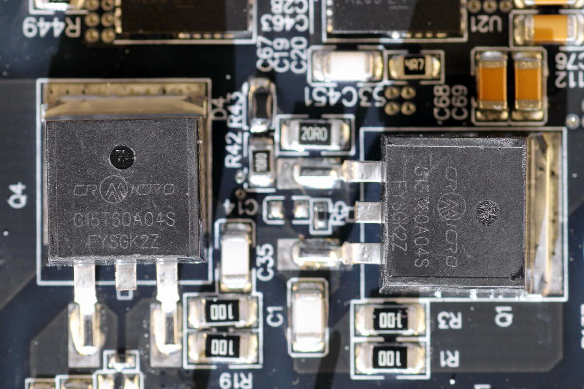
The two IGBTs are from CR MICRO and adopt TO263 package. 600V 15A. Model is CRG15T60A04S.
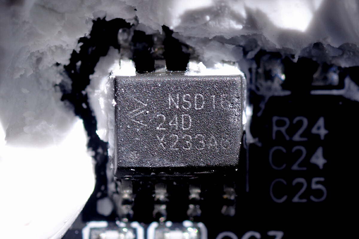
The half-bridge driver is from NOVOSENSE and adopts SOP8 package. It supports TTL and CMOS logic signal input to meet half-bridge, full-bridge, and LLC applications. Model is NSD1624D.
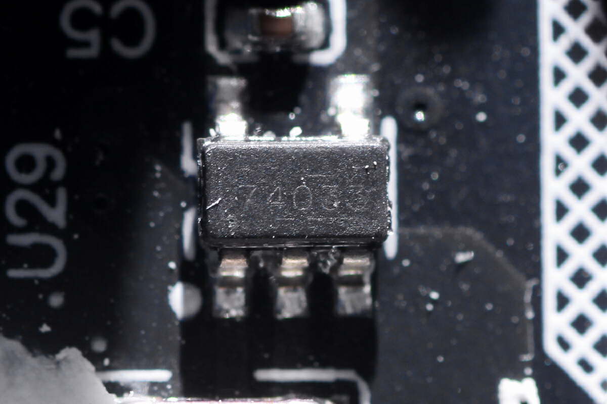
The voltage regulator chip marked with 74033 is from TI and adopts SOT23 package. Its output voltage is 3.3V, output current is 0.3A, and input withstand voltage is 5.5V. Model is TLV74033.
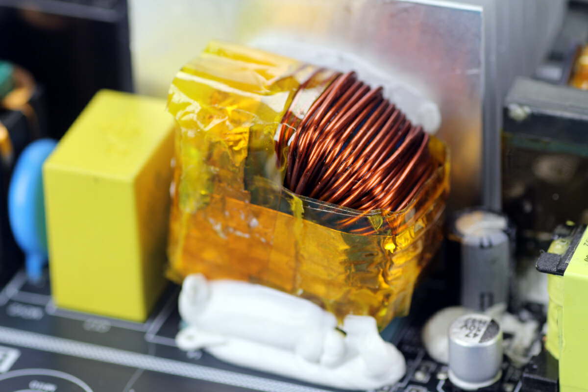
The filter inductor is made of magnetic ring, wrapped with high-temperature tape for insulation, and reinforced with glue.
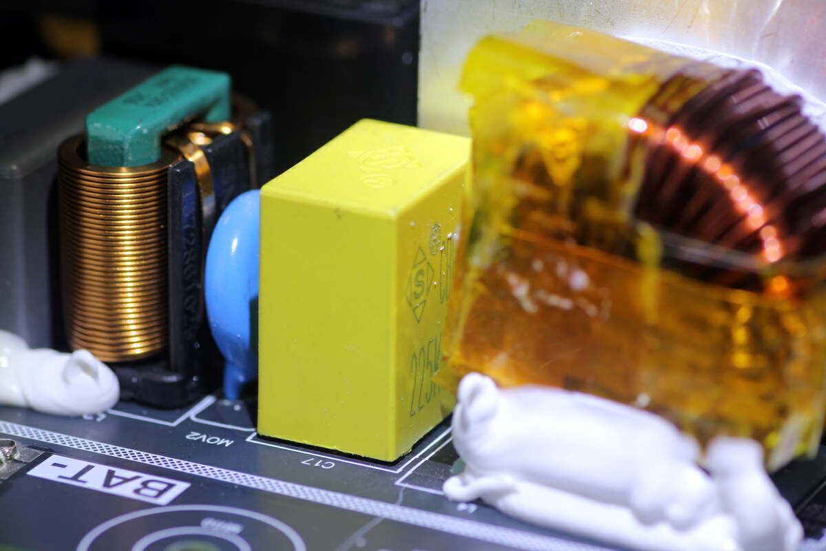
The film capacitor is from STE. 2.2μF.
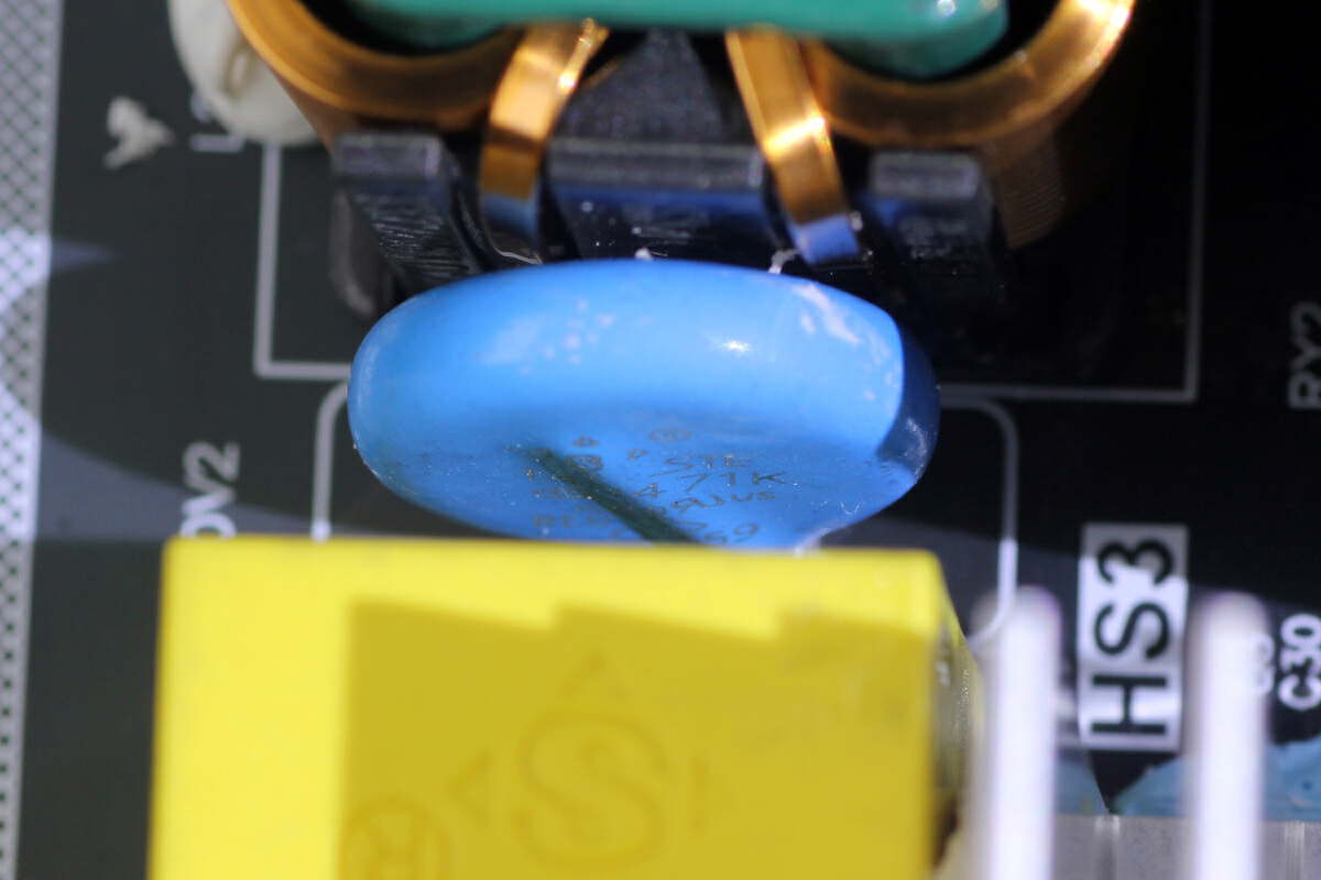
The varistor is used to absorb the overvoltage surge from STE. Model is 14D471K.
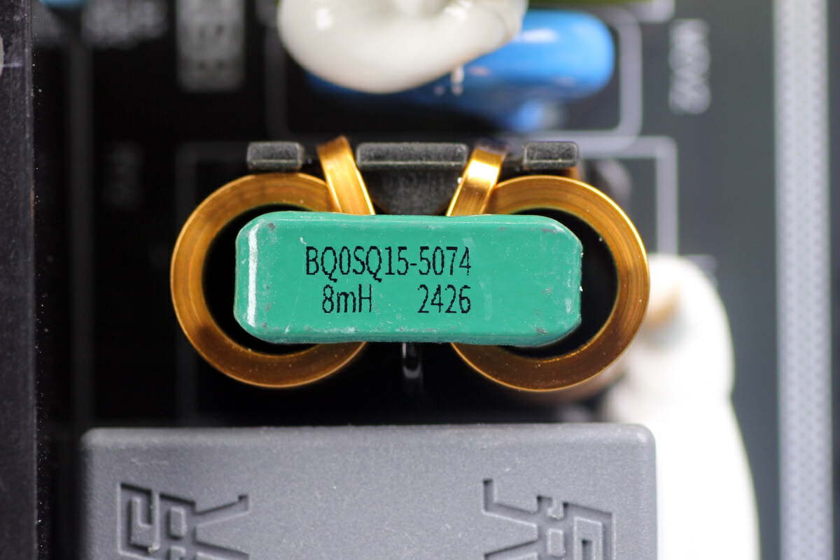
The common mode choke is wound with flat copper wire.
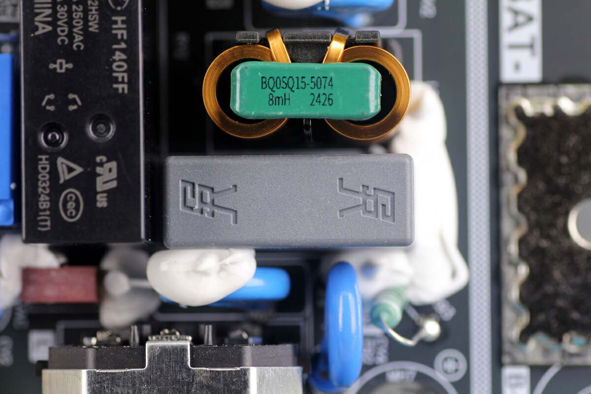
The safety X2 capacitor is from SINCERITY.
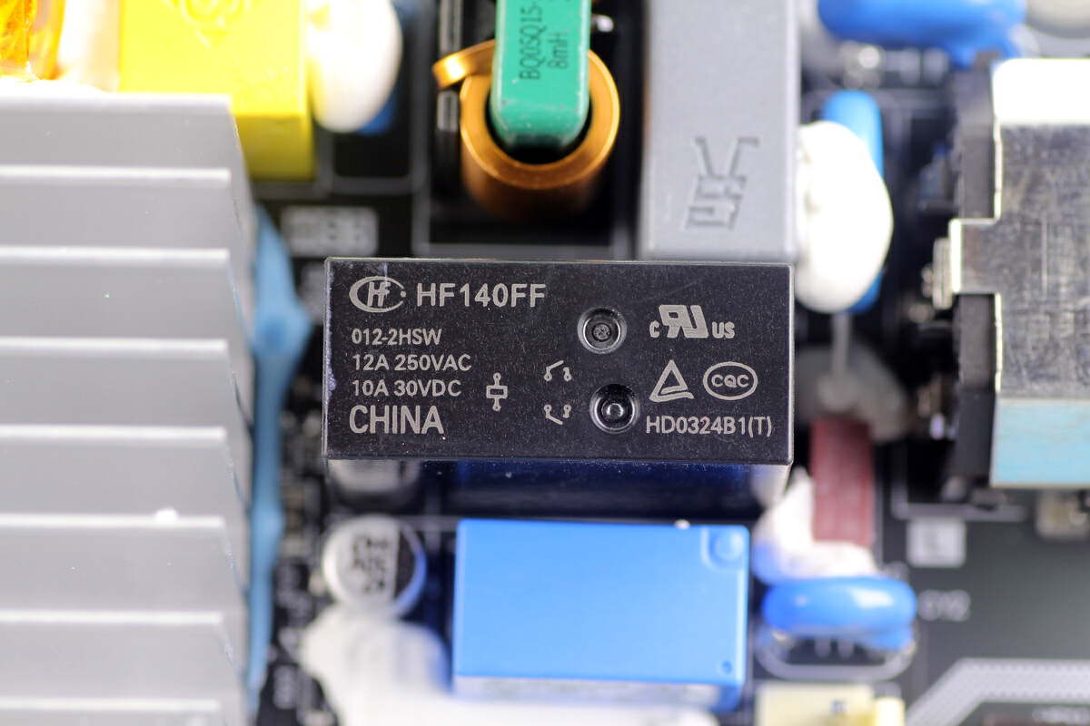
The relay for output switching is from HONGFA. It is a small-medium power relay with a coil voltage of 12V and two sets of normally open contacts built-in. Model is HF140FF/012-2HSW.
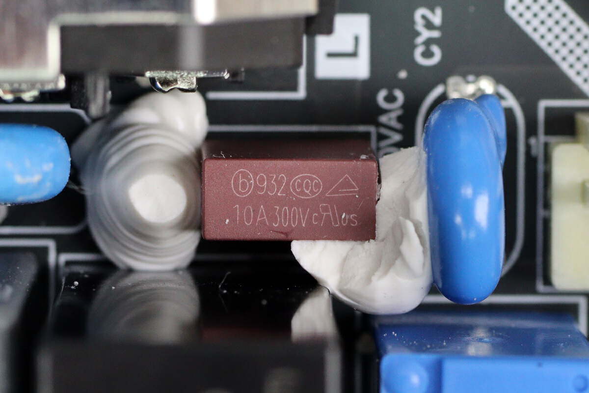
The input fuse is from Betterfuse. 10A 300V.
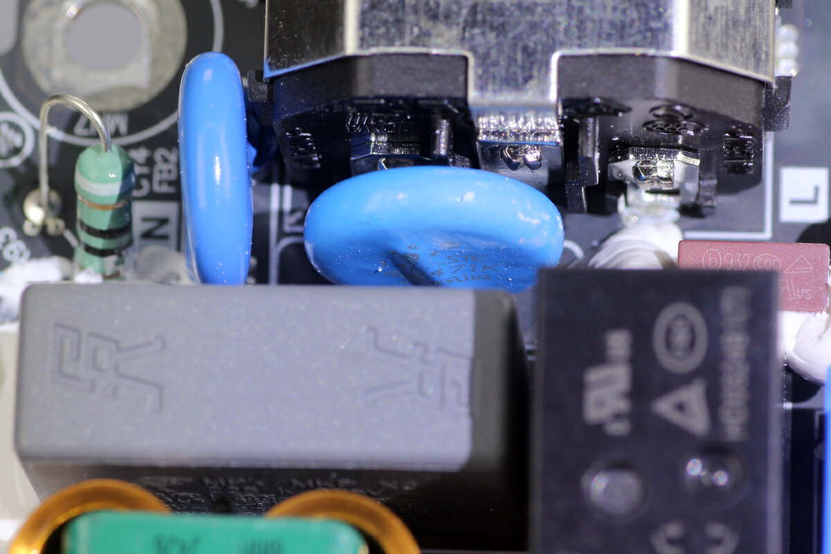
The varistor used to absorb overvoltage surge is from STE. Model is 14D471K,
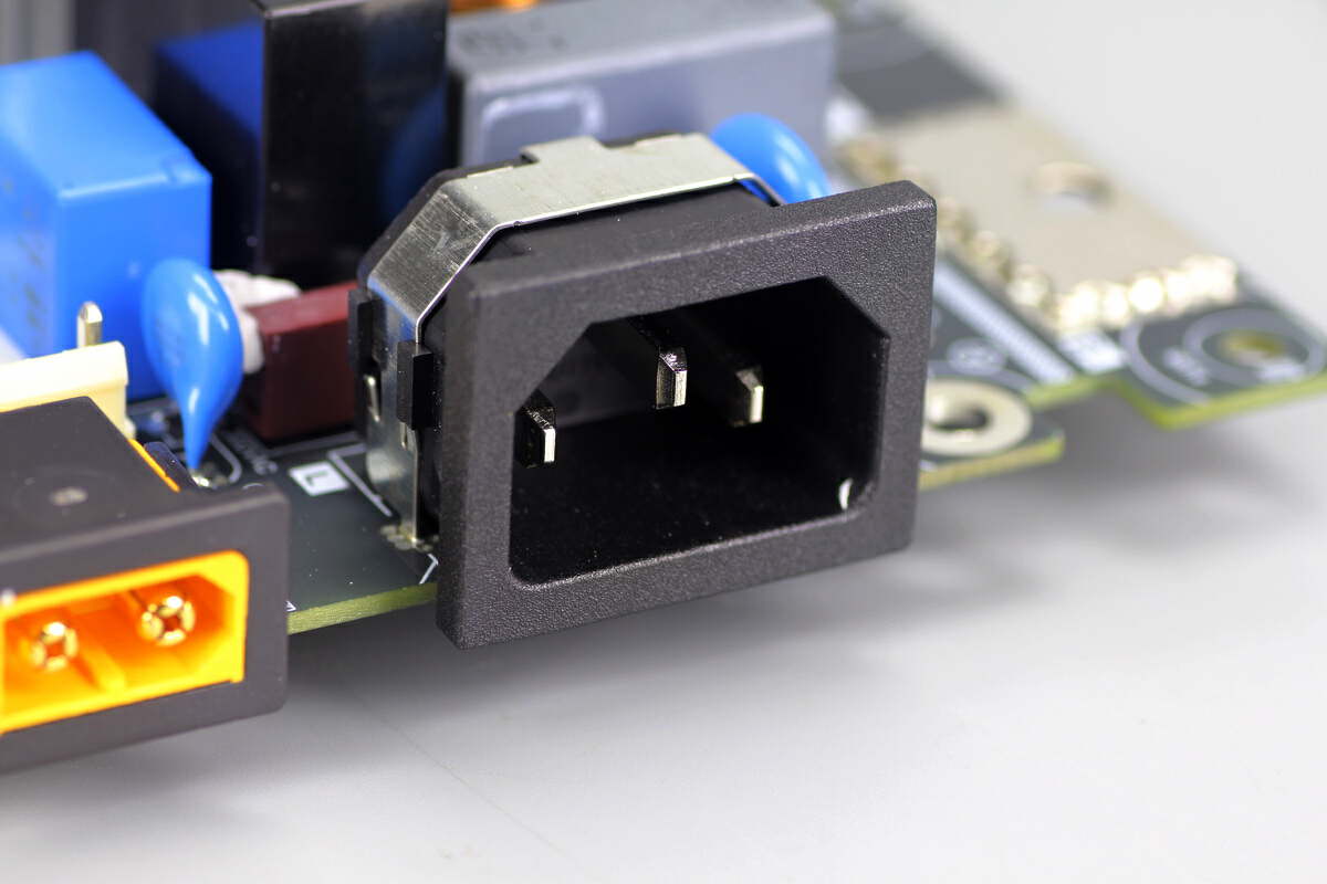
This is the AC input socket.
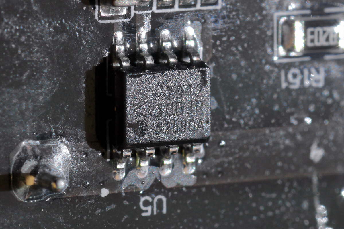
The current sampling chip is from NOVOSENSE and adopts SOIC8 package. It has a range of 30A and a supply voltage of 3.3V. Model is NSM2012-30B3R.
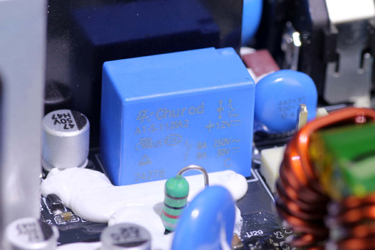
Another relay for AC output control is from Churod.

This is the inverter output socket.
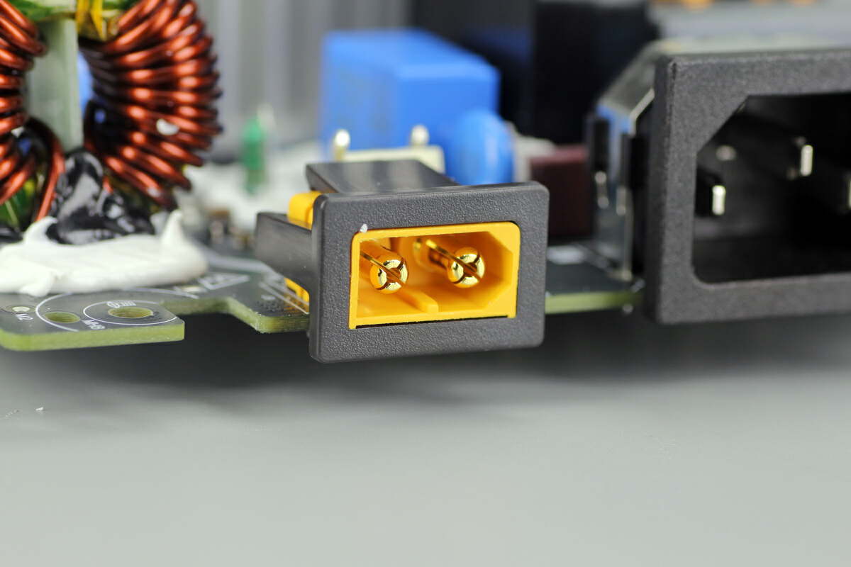
The DC input socket uses an XT60 connector.
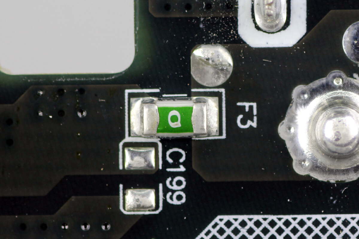
The SMD fuse is used for overcurrent protection.
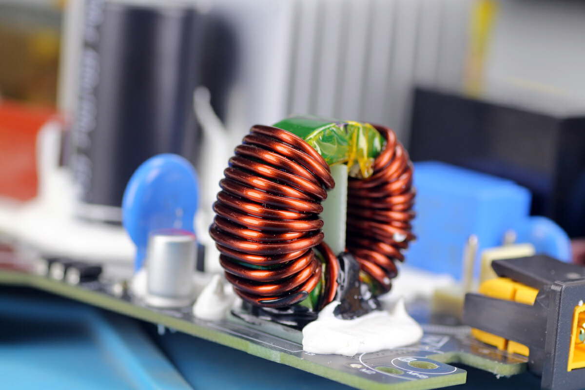
The filter inductor is made of magnetic ring, with bakelite insulation at the bottom and glue reinforcement.
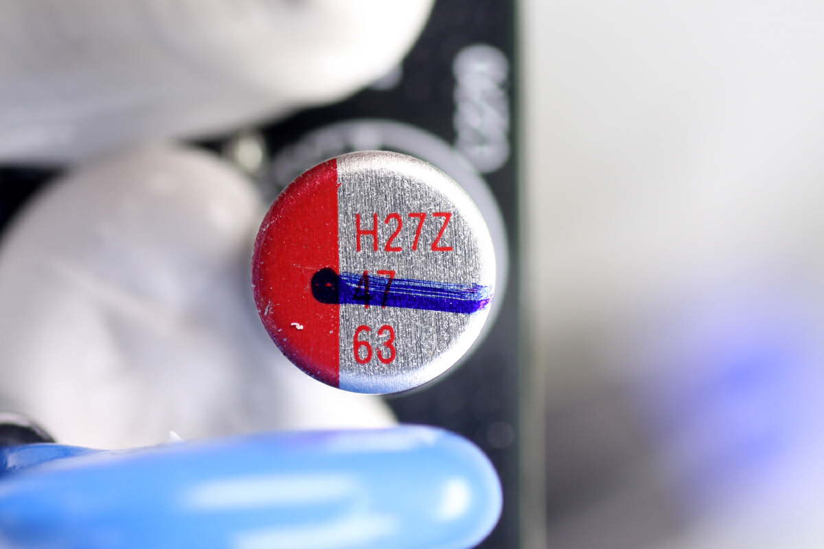
This is the filter capacitor. 47μF 63V.
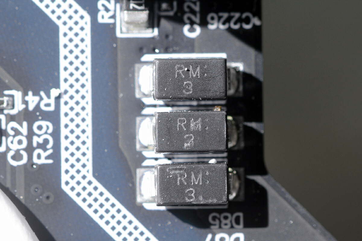
These are three TVS diodes marked with RM.
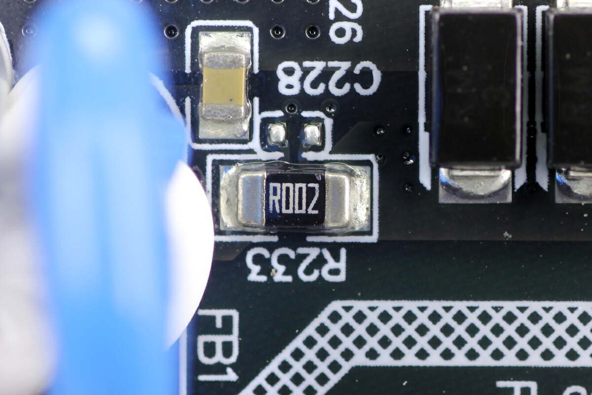
This is the sampling resistor used to sense the input current. 2mΩ.
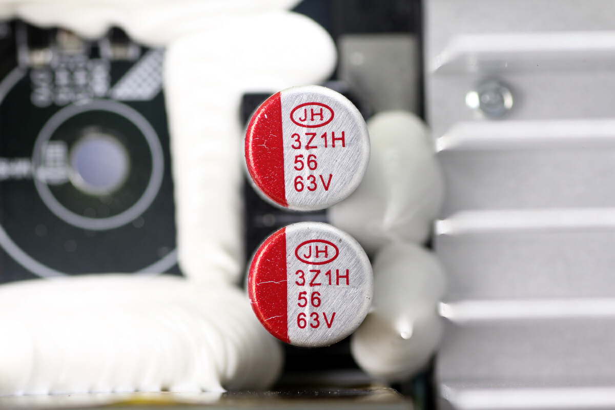
These two filter capacitors are from Jianghai. 56μF 63V.
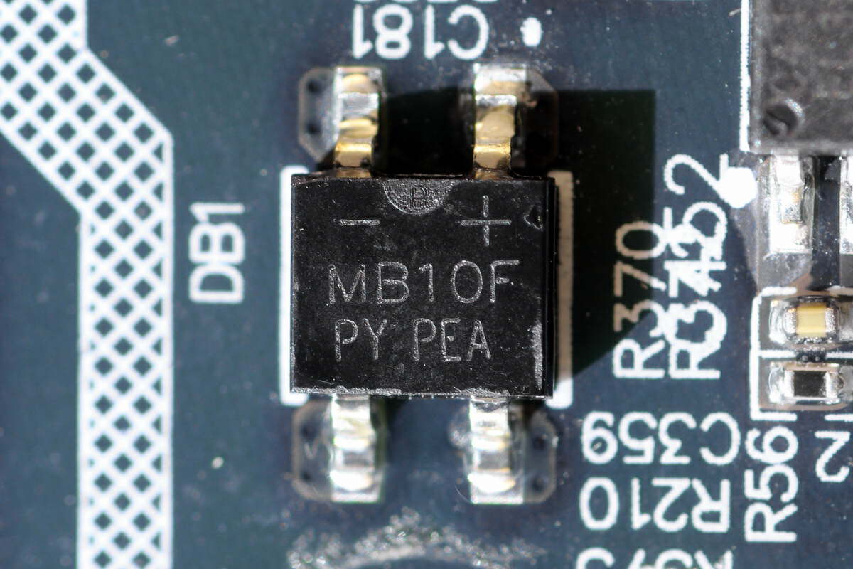
The auxiliary power supply rectifier bridge is from PY and adopts MBF package. 1A 1000V. Model is MB10F.
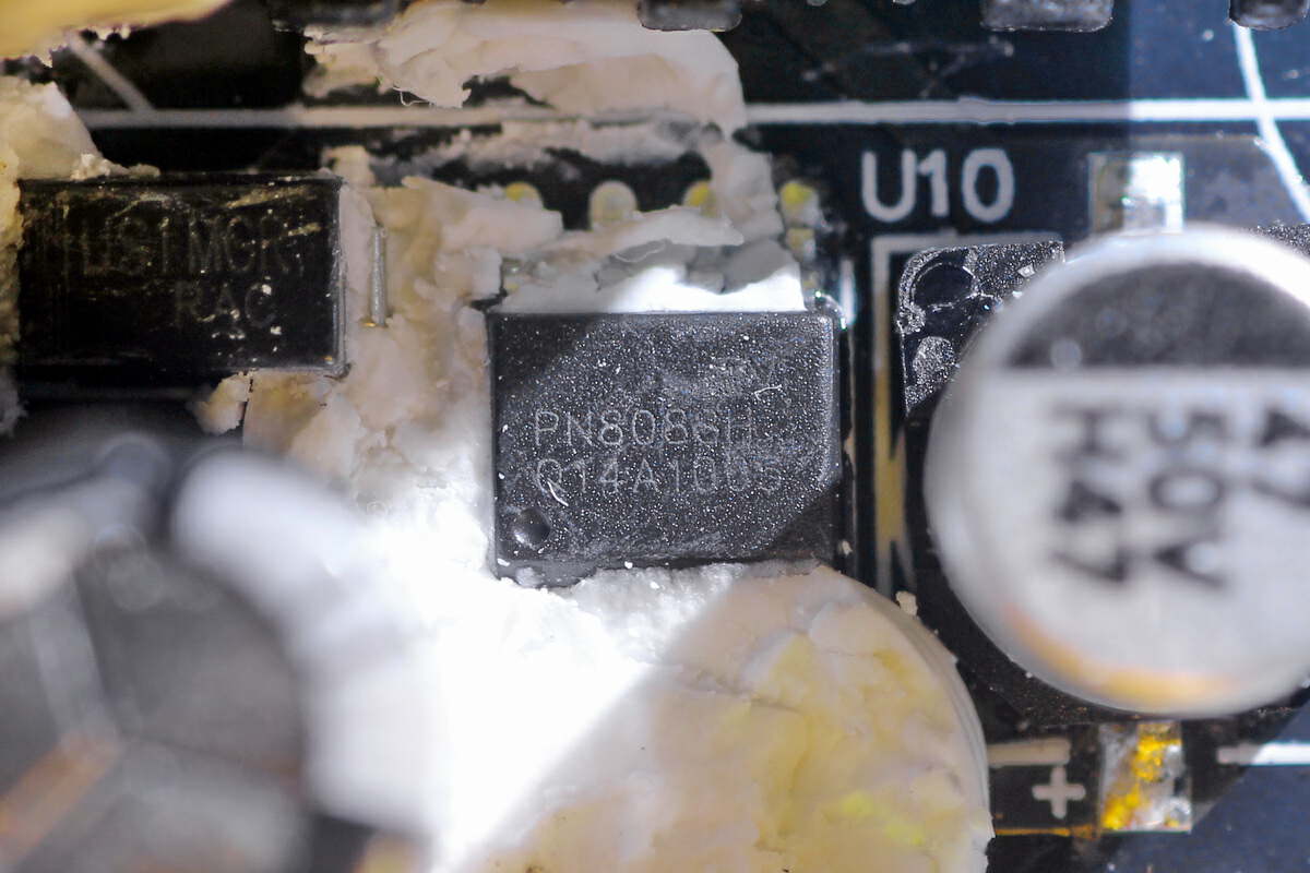
The auxiliary power chip is from Chipown and adopts SOP8 package. It is a low standby power switching power supply chip with an integrated 650V withstand voltage MOSFET for non-isolated flyback switching power supply applications, supporting PWM and burst mode. It has a built-in high-voltage startup, no startup resistor and current detection resistor are required, and it has comprehensive protection functions. Model is PN8083H.
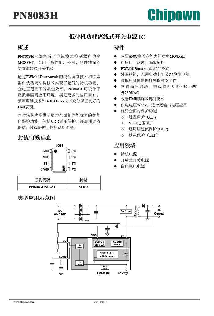
Here is the information about Chipown PN8083H.
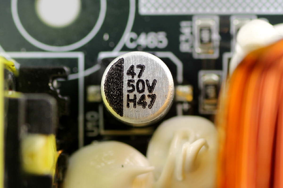
Here is the filter capacitor. 47μF 50V.
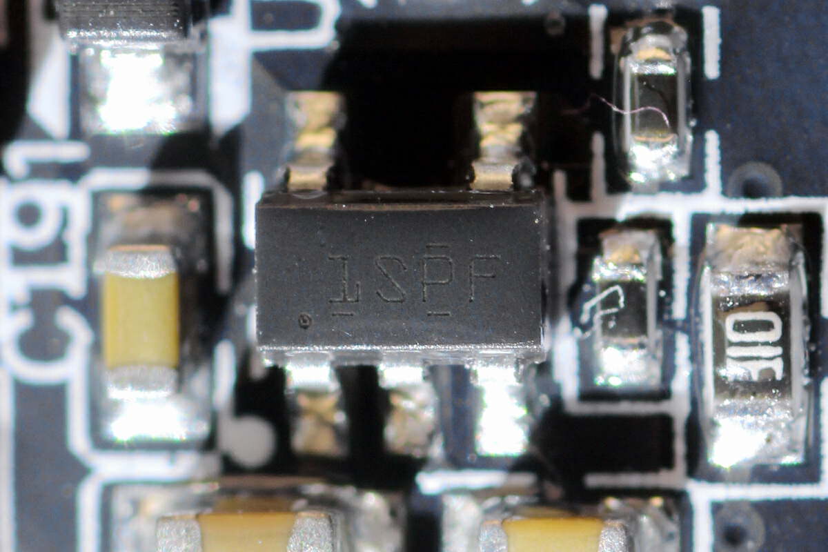
The single op-amp marked with 1SPF is from TI and adopts SOT23 package. Model is LM321LV.
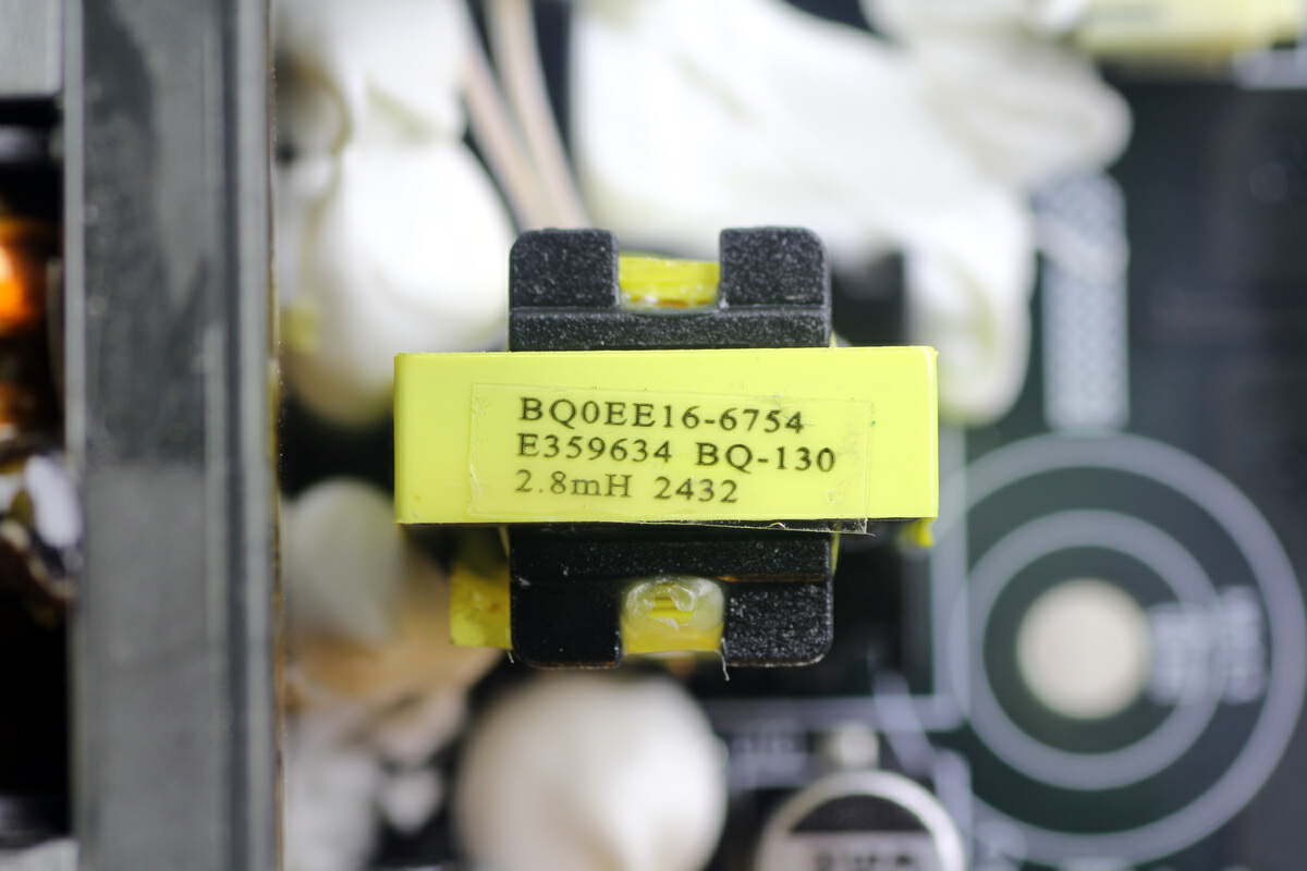
The auxiliary power transformer uses EE16 magnetic core.
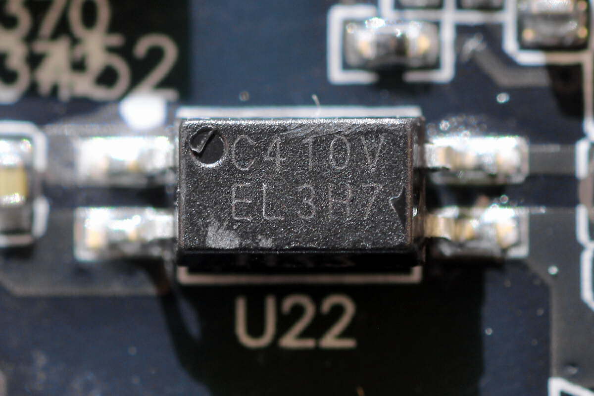
The EL3H7 optocoupler is used for output voltage feedback.
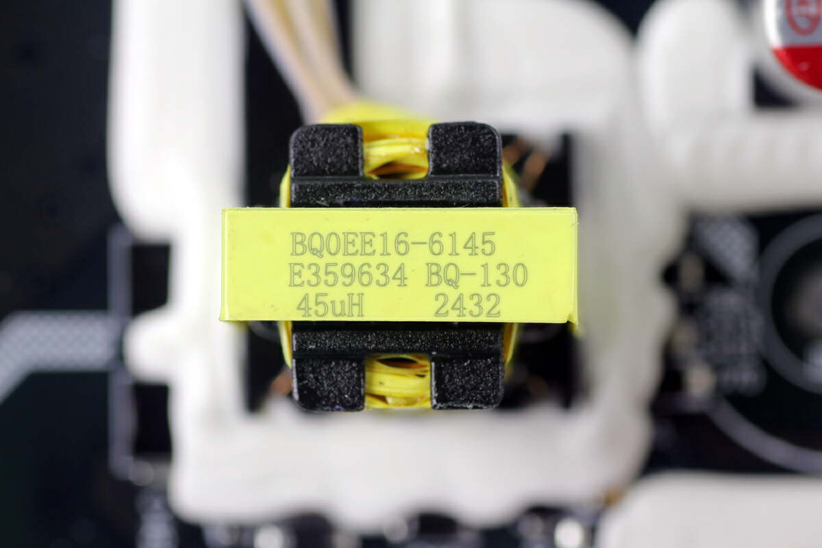
This is another transformer.
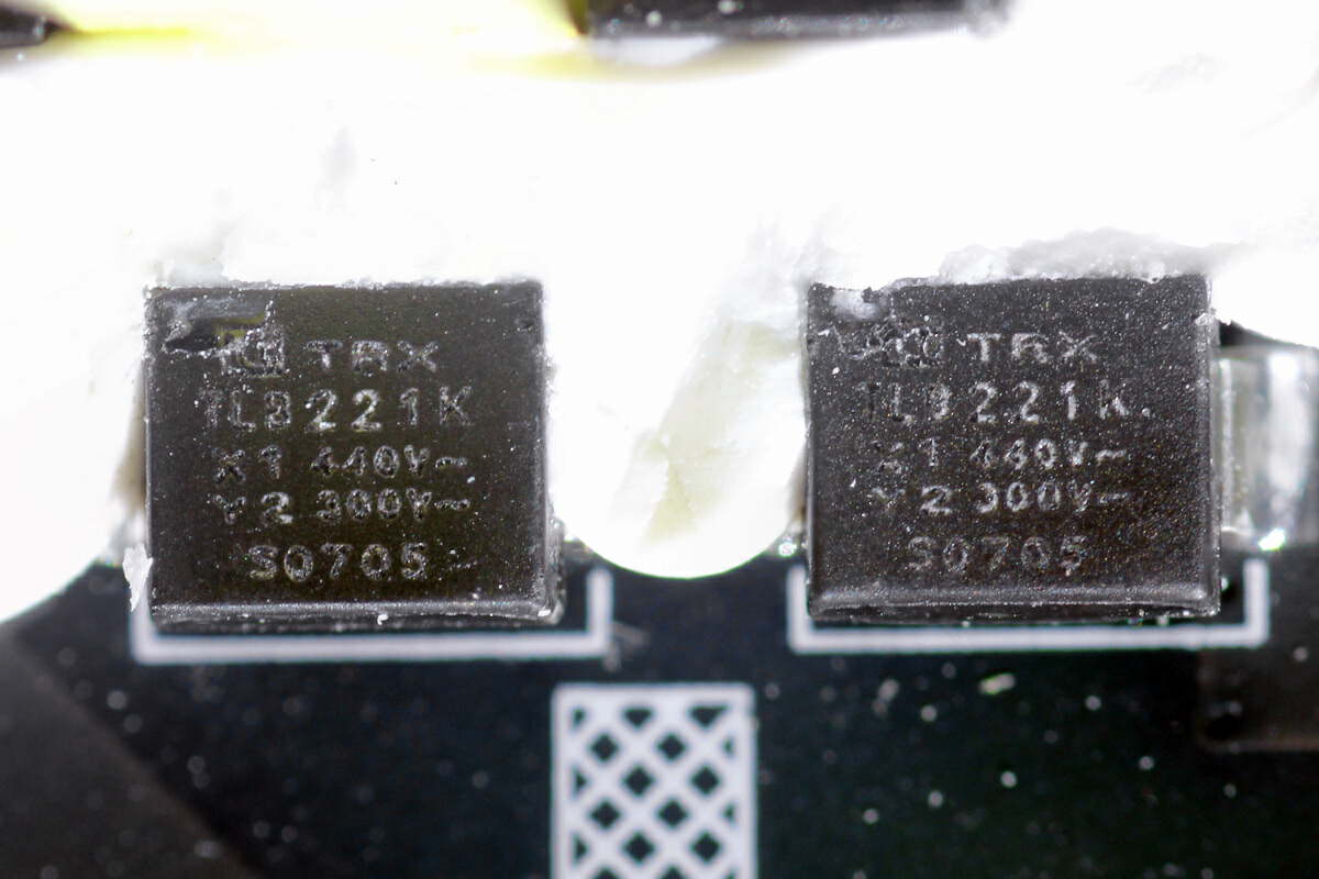
The SMD Y capacitor is from TRX. Its small size and light weight are suitable for high-density power products such as GaN fast chargers.
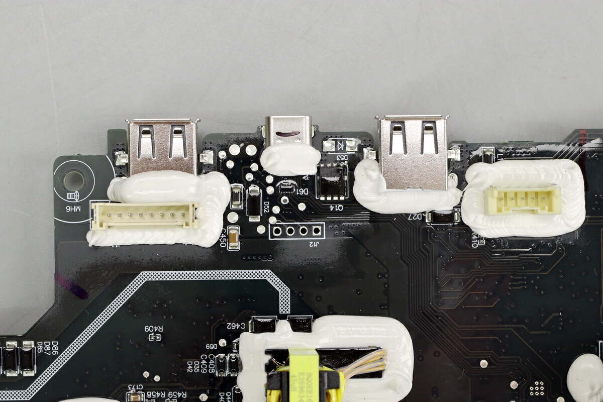
The USB-C and USB-A ports are reinforced with glue.
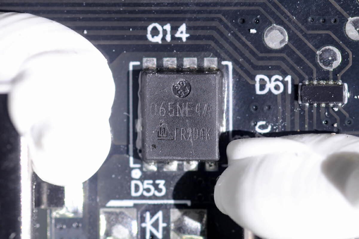
The VBUS MOSFET of the USB-C port is from CR MICRO. Model is HGQ065NE4A.
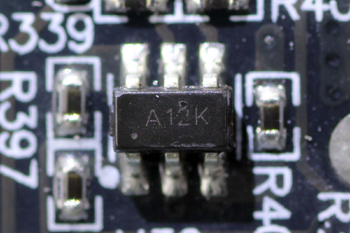
The chip marked with A12K is used for USB-A port protocol recognition.
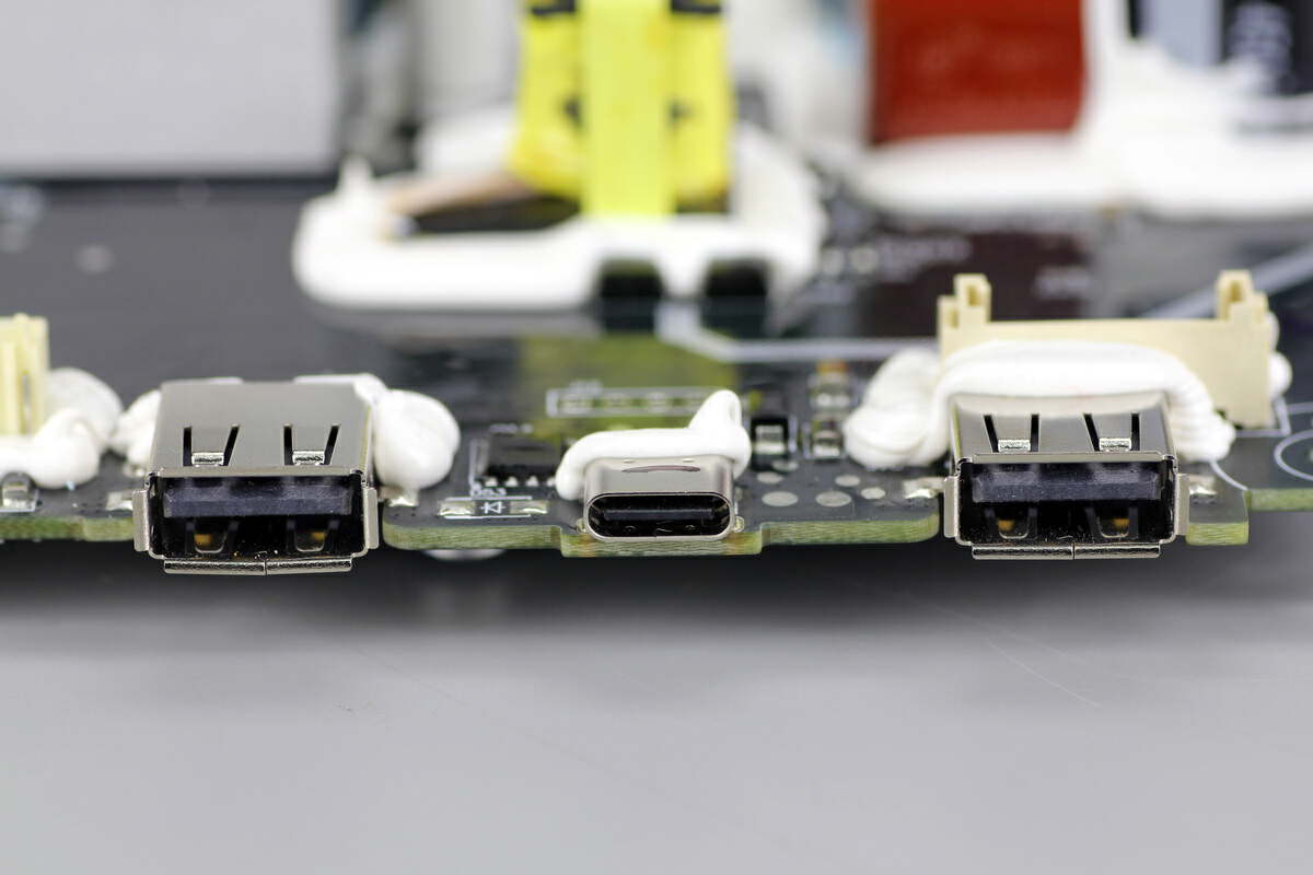
The USB-C and USB-A sockets are fixed by through-hole welding and reinforced with glue.
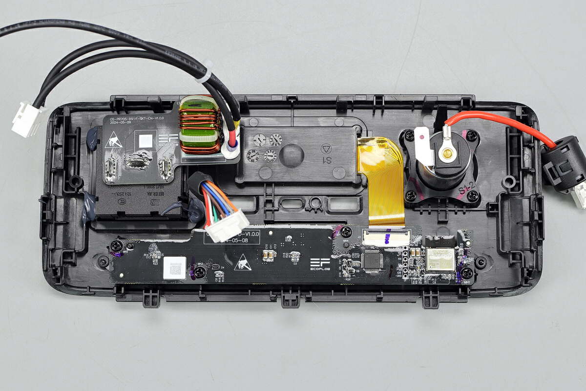
There is a small board inside the front panel for connecting the AC output. The DC output interface on the right is connected by wires. There is an LCD screen in the middle and a control board at the bottom.
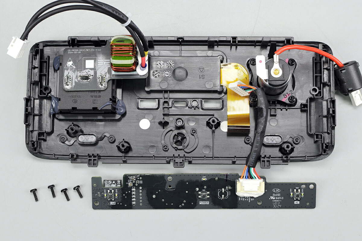
Unscrew the fixing screws and remove the control board.
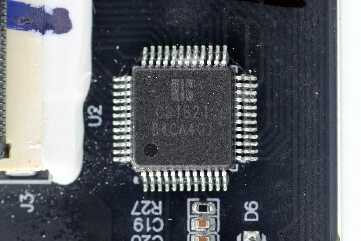
The display driver chip is from i-Core and adopts LQFP48 package. It supports 32 columns and 4 rows LCD drive control. Model is CS1621.
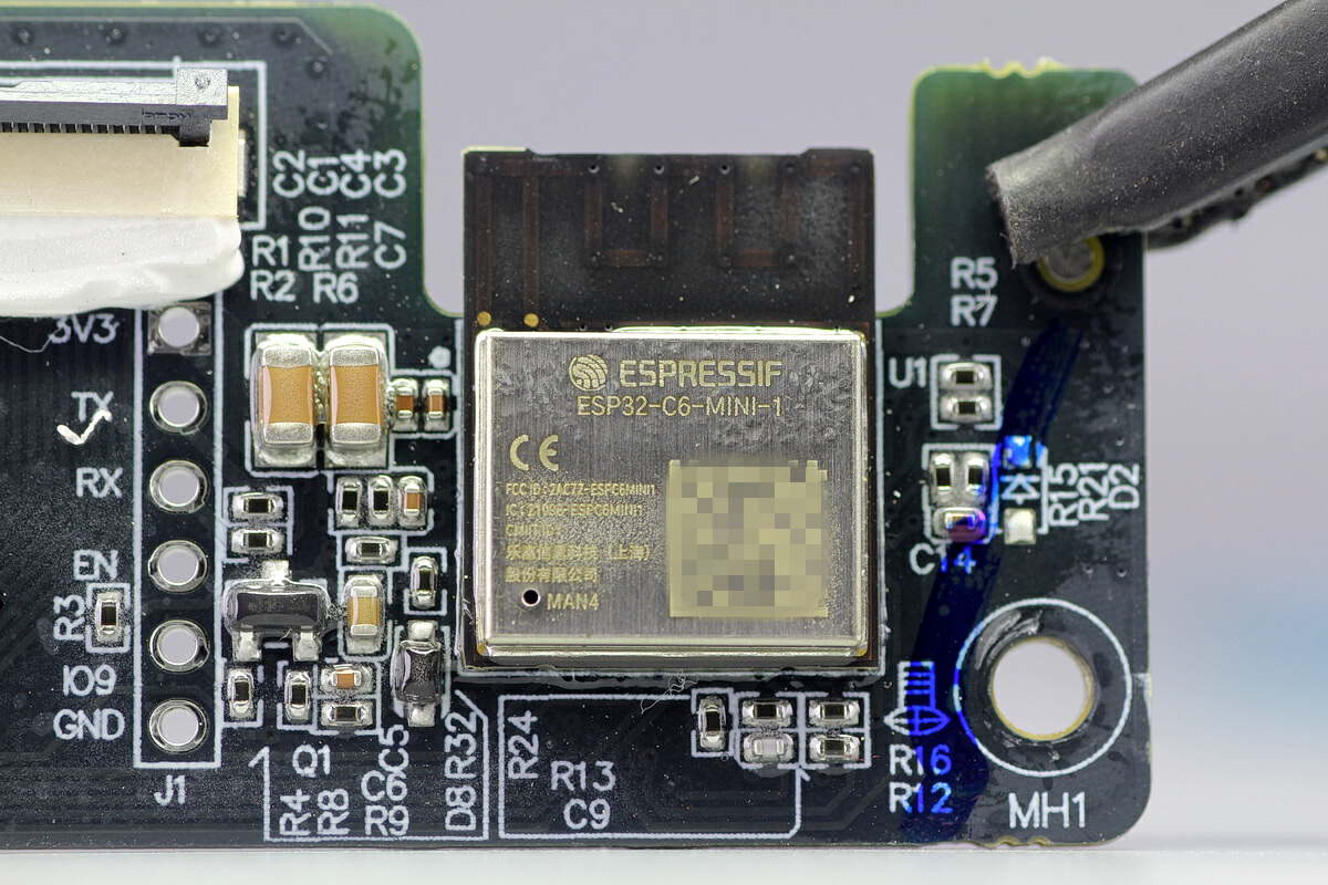
The wireless communication module is from ESPRESSIF. It has a built-in ESP32-C6 series chip, a built-in RISC-V 32-bit single-core processor, an onboard PCB antenna, and supports WiFi6 and Bluetooth BLE connections. Model is ESP32-C6-MINI-1.
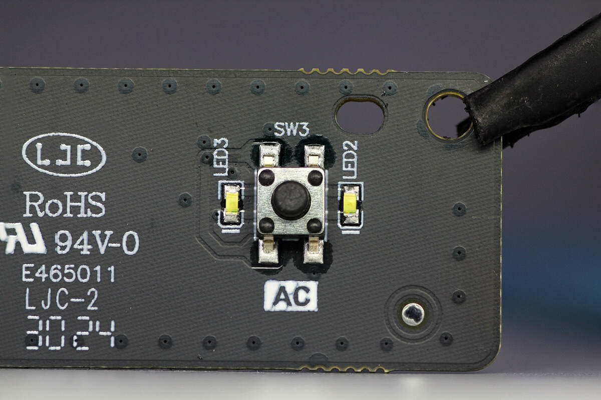
There are LED indicators on both sides of the micro switch.
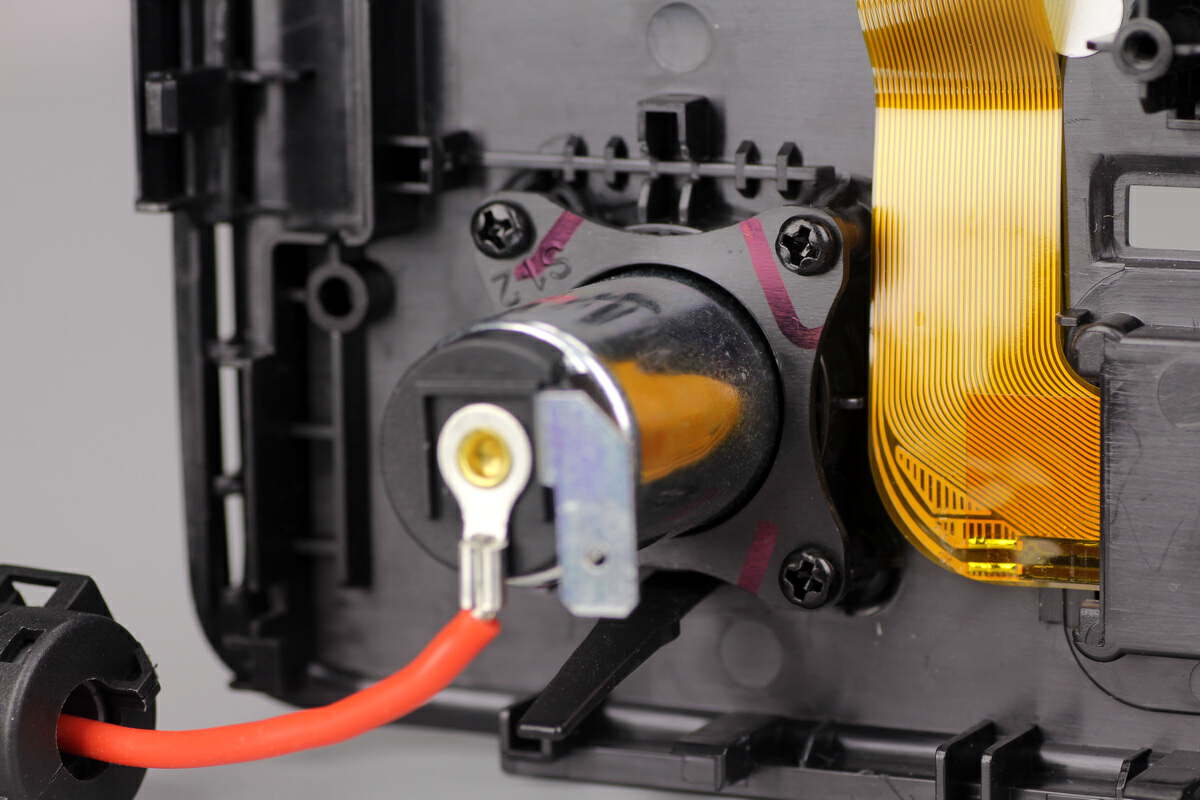
The positive wire of the car charger interface is connected by crimping.
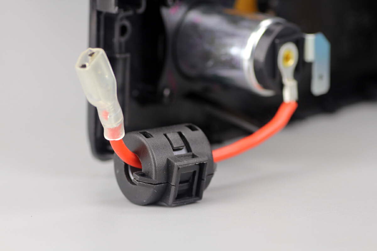
The wire passes through the magnetic ring to suppress interference.
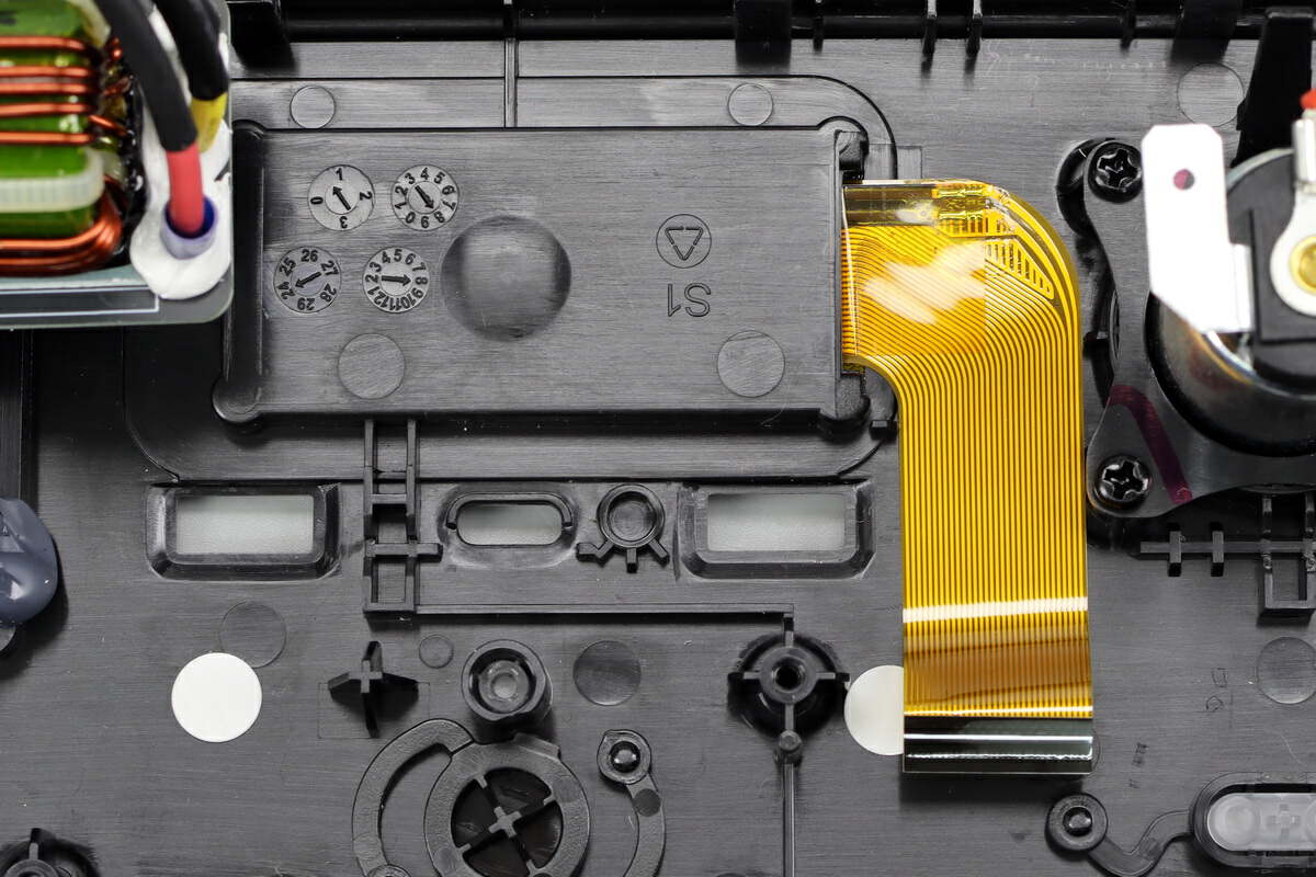
The LCD screen is connected via a cable.
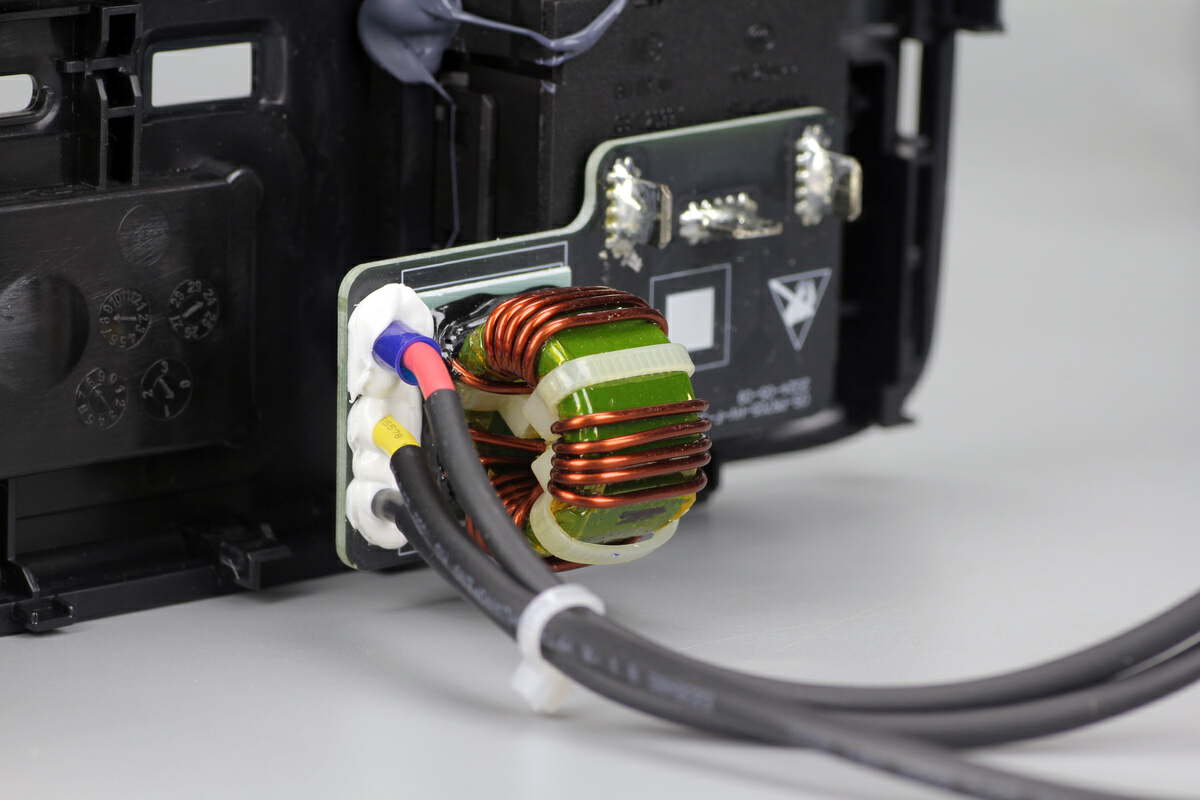
The AC output is filtered by a magnetic ring inductor.
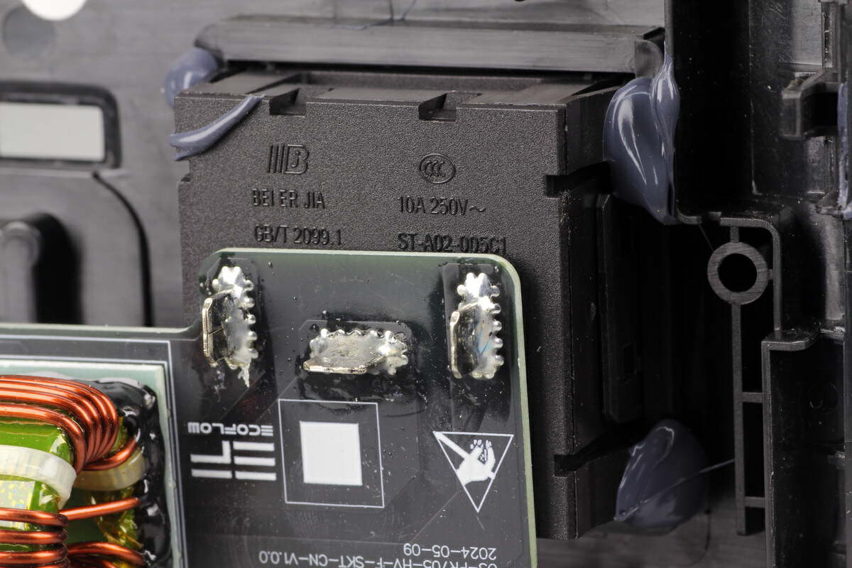
The AC output socket is connected by welding.
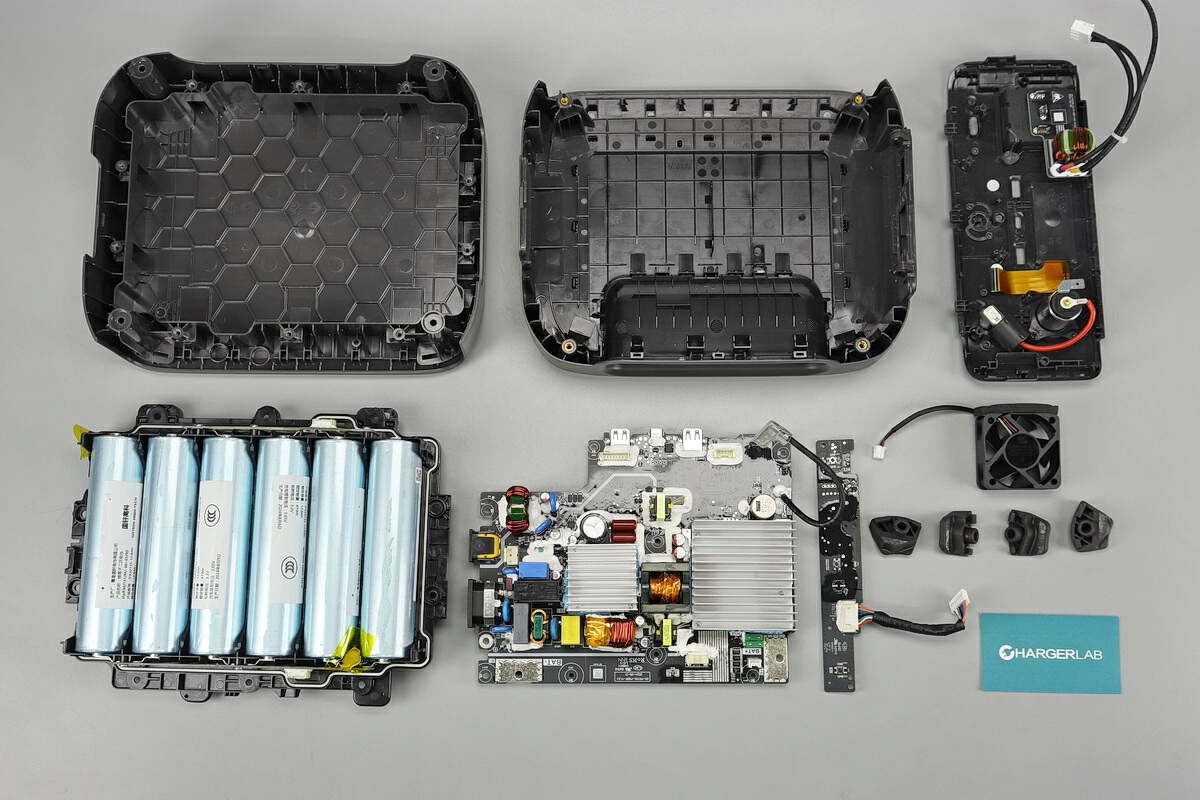
Well, those are all components of the ECOFLOW RIVER 3 300W 245Wh GaN Power Station.
Summary of ChargerLAB
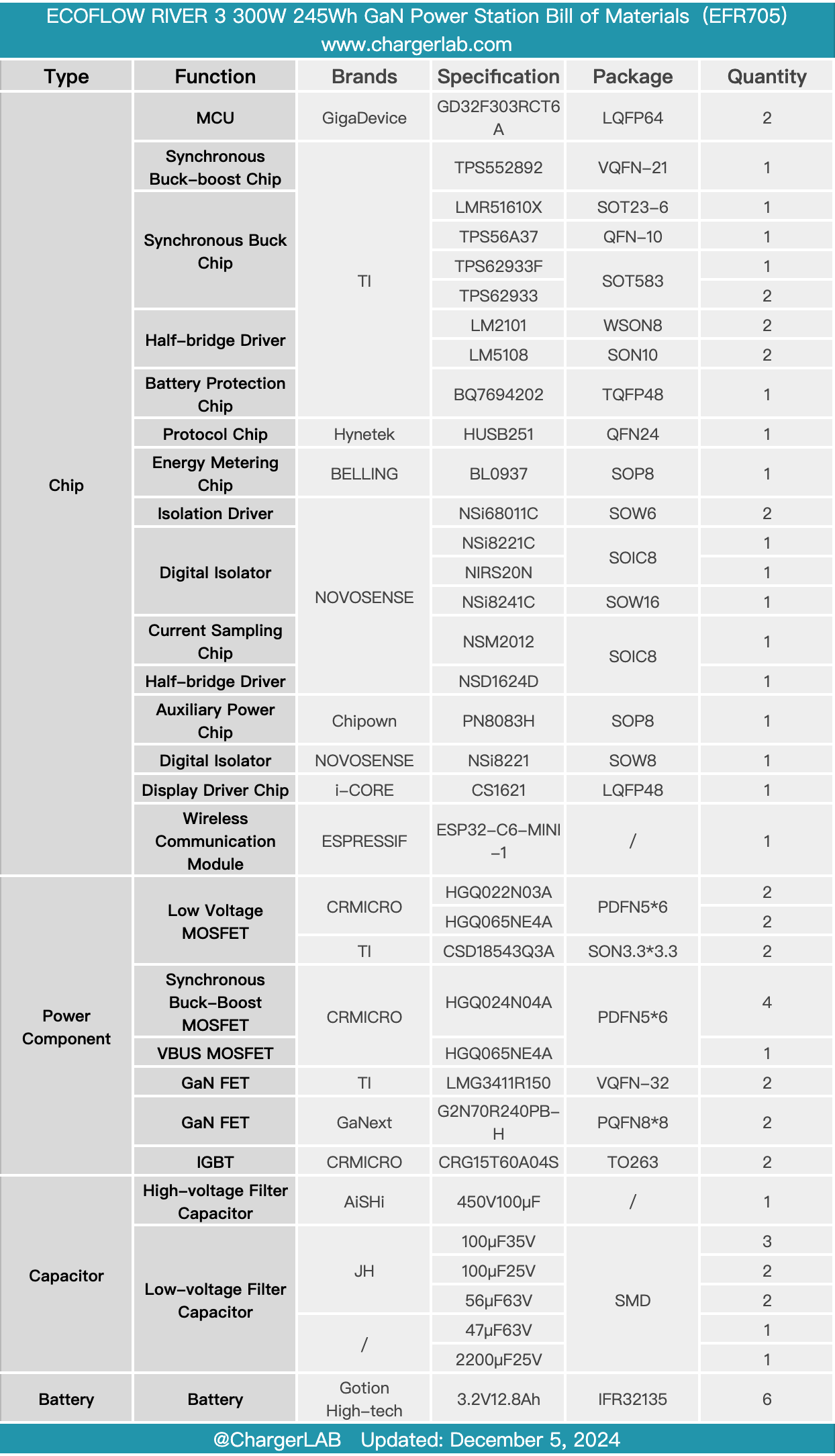
Here is the component list of the ECOFLOW RIVER 3 300W 245Wh GaN Power Station for your convenience.
The ECOFLOW RIVER 3 power station has a built-in 245Wh lithium iron phosphate battery. Its built-in bidirectional inverter module supports 300W charging power and 300W output power. The upgraded drive supports 600W power. It also supports DC input and can be charged with solar panels or car chargers. The USB-C port supports 100W PD fast charging. There is an LCD screen on the side to facilitate information such as remaining usage time, remaining power, and input and output power.
After taking it apart, we found it uses a modular design, the battery pack is dustproof and waterproof, with IP54 protection. The battery pack uses six strings of lithium-iron phosphate batteries. The batteries are connected by nickel strip spot welding, and a thermistor is set to detect the temperature.
It has a bidirectional inverter circuit, battery protection circuit, and fast charging circuit, realizing all functions. The PCBA module is covered with conformal coating and thermal conductive adhesive to prevent moisture and dust from affecting it and ensure operational reliability.
Related Articles:
1. EcoFlow Launches New DELTA Pro 3 Series with X-CORE 3.0 Technology for a Revolutionary Experience
2. Up to 6 kWh | Introducing the EcoFlow DELTA 2 Max Extra Battery Kit
3. EcoFlow Launched GLACIER Portable Refrigerator & WAVE 2 Portable Air Conditioner

