Did you remember that we have torn down the first Dell 90W GaN charger before? If you haven't seen it, you can click here to view it.
Recently, ChargerLAB got a new model, which is Dell 60W Power Adapter. It adopts ACF topology and integrates two GaN ICS (Navitas NV6115 and Navitas NV6117).
Compared to the 90W model, which still adopts the traditional size, this one is much smaller and easier to use. So, it’s more suitable for people who travel a lot.
Today, we will tear it down to see the internal structure and components.
1. Appearance

It continues the traditional design of Dell 90W charger.
Just like the mini version of 90W charger without the cable.

The DELL logo is on the front.

The indicator light is near the output.

The specs information is printed on the back.

Model is HA60NM200.
It supports input of 100-240V~50/60HZ 1.7A and output of 5V3A, 9V3A, 15V3A, 20V3A.
Manufactured by Chicony Power.
It also passed different safety certifications, such as CCC, CE, CP, EAC, UKCA, GS, UL, PSE, NOM, KC, TUV., etc.

Here is the standard 3-prong receptacle, including the ground wire.

And the other side adopts the detachable design, USB-C port.
So, you can even use your own USB-C cable.

The length of the adapter is 66mm (2.6 inches).

Width is 55mm (2.17 inches).

And thickness is 22mm (0.86 inches).

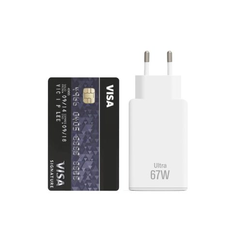
Compared to Apple 61W charger, the size is much smaller.

This is how you hold it.

The weight is about 101g (3.56 oz).

Then, let's use ChargerLAB POWER-Z KT002 to test the protocol.
USB-C only supports PD3.0

And it can support four PDOs of 5V3A, 9V3A, 15V3A, 20V3A.
2. Teardown

Let's use the cutting machine to open it.
The charger module is covered with copper heat sink.

And the insulating plate is between the heat sink and the components.

The heat sink is fixed by clips. And then we can remove it.

The length of the adapter is 60.89mm (2.4 inches).

Width is 49.58mm (1.95 inches).

And thickness is 18.26mm (0.72 inches).

The ground wire is protected by insulating tube and across the primary and secondary circuits.

Here is the front of the PCB. The transformer is in the middle. And the capacitor and inductor are on two sides.

Turn to the back, the primary circuit is on the right, and the synchronous rectifier circuit is on the lower-left corner.
The bridge rectifier, SMD Y capacitor, and optocoupler are in the middle.
ChargerLAB found this charger adopts the high-frequency ACF topology, and uses the protocol chip to control the output voltage.
Let's start to analyze the internal components.

Here is the input end. The time-delay fuse, safety X capacitor, and a common mode choke are on the left. And a small common mode choke and filter inductor are in the middle.

The specs of time-delay fuse are 3.15A 250V.

The capacity of safety X capacitor is 0.33μF.

This common mode choke is used to filter out EMI interference.

The other one is wound by two wires.

Here is the bridge rectifier, marked with MB30M.

And this is the filter inductor.

Turn to another side, here is an electrolytic capacitor for high-voltage filtering and the capacitor of the master control chip.

The electrolytic capacitor comes from SAMXON, 400V 100μF.

The capacitor of master control chip comes from LTEC.

35V 56μF.

The master control chip adopts Texas Instruments UCC28782, which is a high-density active clamp flyback (ACF) controller with EMI dithering, X-Cap discharge, and bias power management.
The maximum operating frequency can reach 1.5MHz, and the efficiency can beyond 93%.
It also supports over-heating, over-voltage, over-current, short circuit protection.

This is the half-bridge driver. Model is ON Semiconductor NCP51530.
It is a 700 V high side and low side driver with 3.5 A source & 3 A sink current drive capability for AC−DC power supplies and inverters.
It can offer best-in-class propagation delay, low quiescent current, and low switching current at high frequencies of operation.
It has two versions, A or B. Version A has a 60 ns delay, while version B only has a 25 ns delay.

Those two GaN ICs on the primary circuit come from Navitas and adopt the QFN 5*6mm Package.
This one is Navitas NV6115, which integrates the driver and complex logic control circuit.
So, it doesn’t need additional external components, saving space and reducing size. And switching frequency can be up to 2 MHz. The specs are 170mΩ, 650V.

Info of Navitas NV6115.

The other one is Navitas NV6117, which also integrates the driver and complex logic control circuit. And switching frequency can be up to 2 MHz. 120mΩ, 650V.

Info of Navitas NV6117.

Here is the transformer.

The optocoupler adopts EverLight EL1018, used to communicate and regulate output voltage.

Here are four SMD Y capacitors.

Then, let's take a look at the synchronous rectifier circuit.

The synchronous rectifier controller comes from MPS MP6908A.
The maximum switching frequency is 600 kHz.
It supports different working modes and can work with standard and logic level synchronous MOSFETs.
Programmable ringing detection circuitry prevents the MP6908A from turning on falsely at VDS oscillations during discontinuous conduction mode (DCM) and quasi-resonant operation.

The synchronous rectifier adopts Infineon BSC093N15NS5, which adopts G-TDSON-8 package.
Withstand voltage 150V, resistance 9.3mΩ.

Here is the 1R0 filter inductor.

Close-up of LED indicator light.

Here is the output. The solid capacitor is wrapped with insulating tape.

The specs of solid capacitor for output filtering is 25V 680μF.

The protocol chip is a customized model, marked with DPD021P.
The nearby thermistor can detect the internal temperature.

This is AOS output VBUS MOSFET, marked with 32308C.

Finally, the durable USB-C receptacle is protected by steel plate.

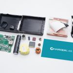
OK, that’s all for the Teardown of Dell 60W mini GaN charger. Let’s take a “family portrait.”
Summary of ChargerLAB
The detachable cable design is the most attractive feature, making this charger more like a phone charger than a laptop charger. And you can choose any USB-C cable you'd like.
It adopts the high-performance ACF topology. Its controller comes from Texas Instruments and MPS.
And the ON Semiconductor driver works with two Navitas GaN ICs (NV6115 and NV6117), which can prove the quality of Navitas GaN IC. The synchronous rectifier comes from Infineon.
All those components come from well-known brands.

