Introduction
ChargerLAB disassembled a Dell 60w USB-C GaN power adapter about two years ago.
We recently got the Dell 165W PD3.1 GaN Power Adapter.
This time, we are going to take it apart to see if there are any differences in built quality and how the internal components look like.
Product Appearance
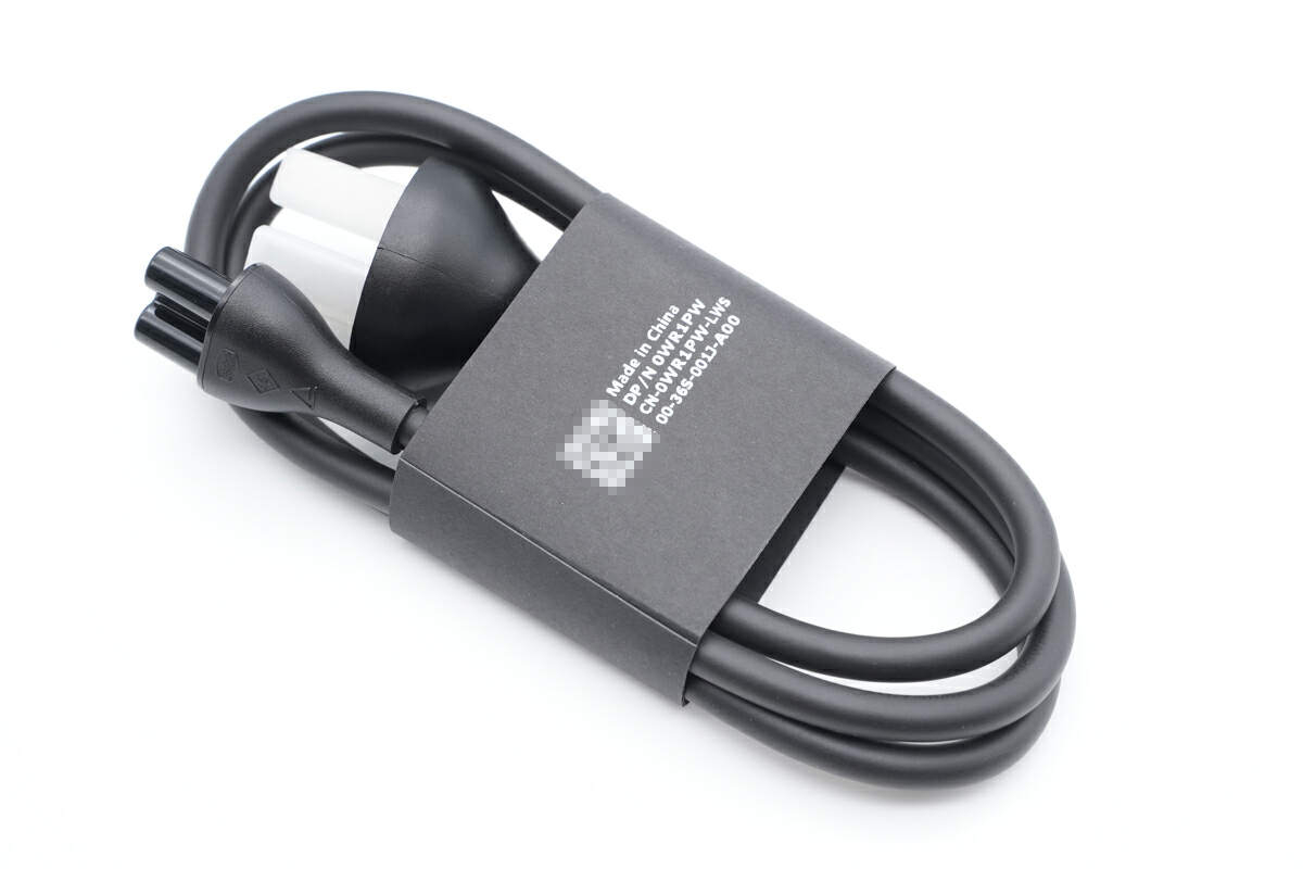
The input cable adopts a detachable design. The plug has a plastic cap for protection
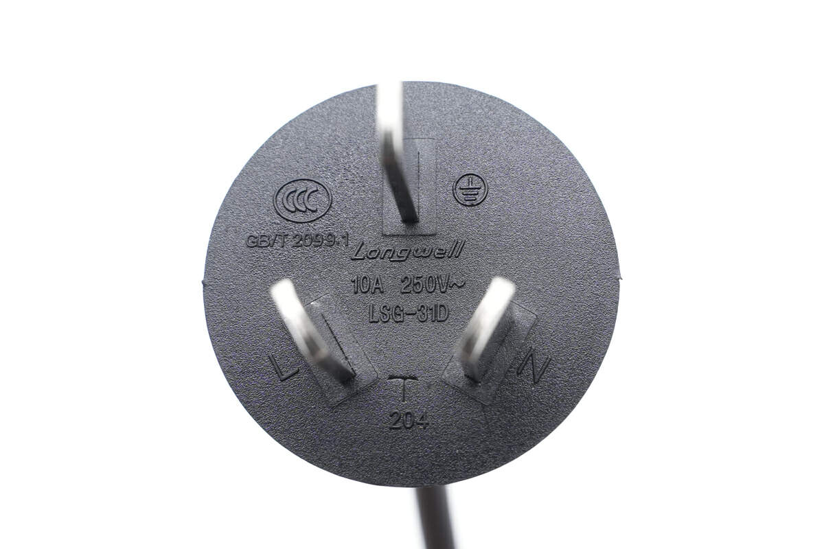
It adopts a three-prong design and is from Longwell, supports 10A 250V~.
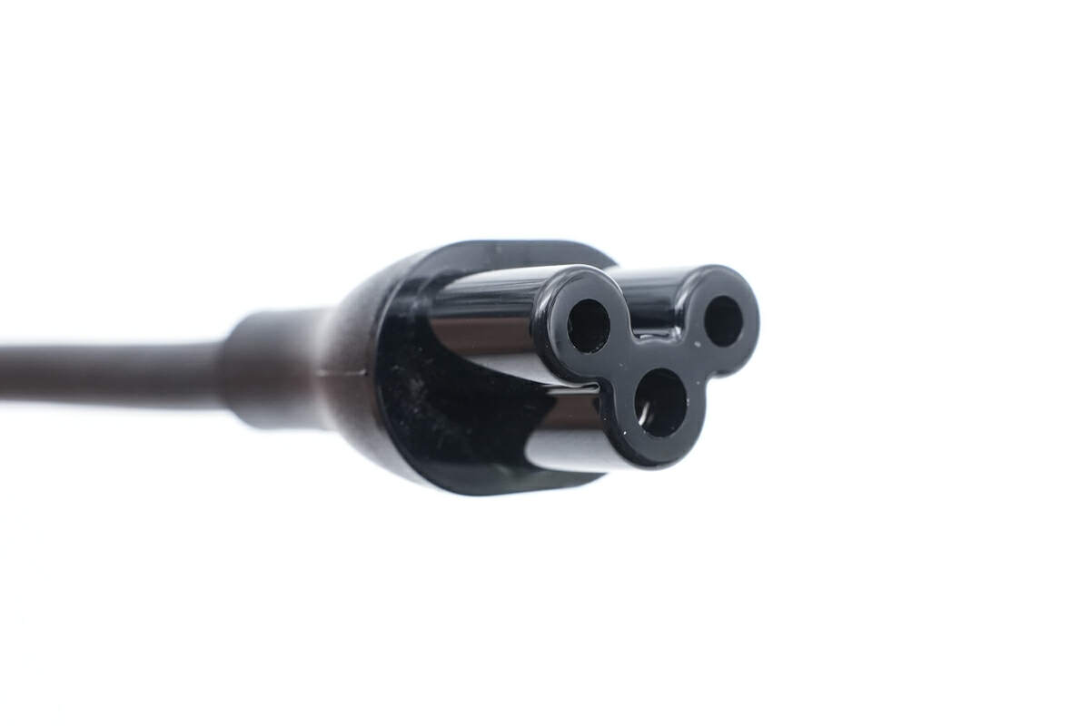
The other side also adopts a 3-prong design.
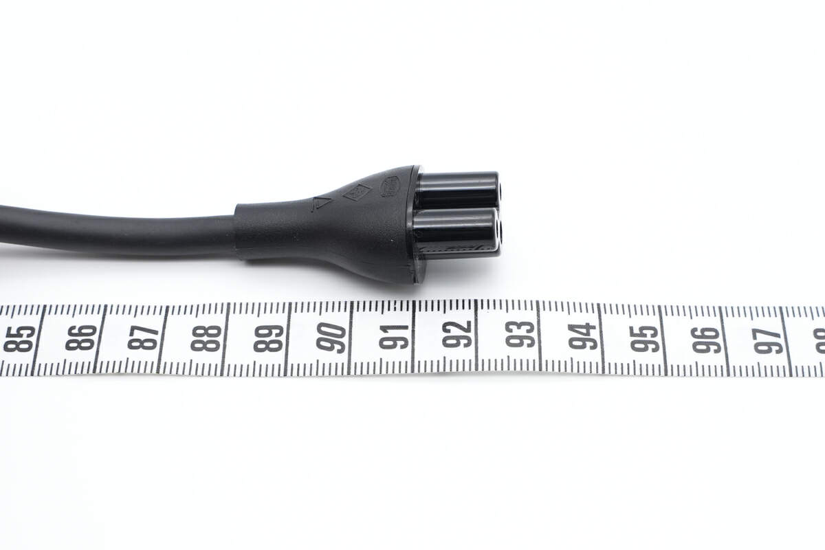
The length of the input cable is about 92cm (3.02 ft).
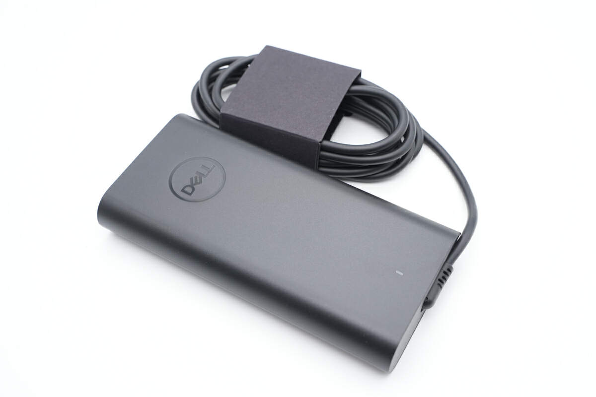
The power adapter is strip-shaped and comes with a detachable USB-C cable.
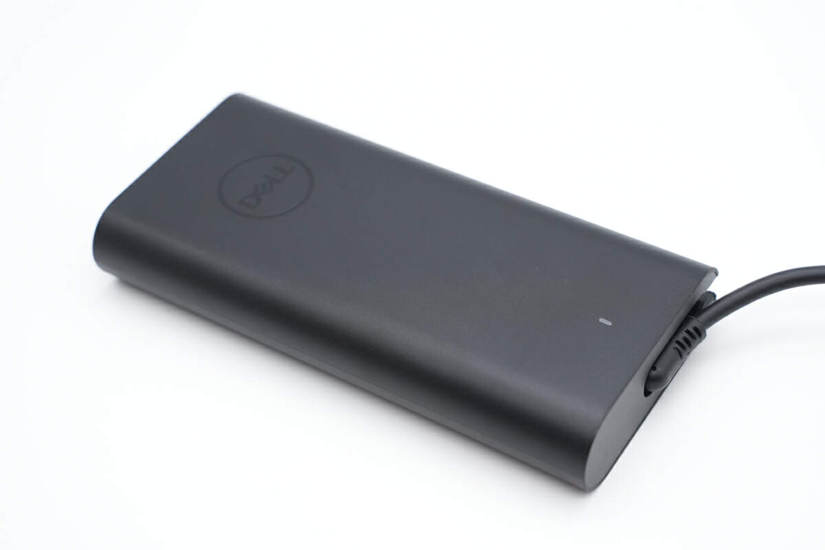
Its fireproof casing adopted a matte design.
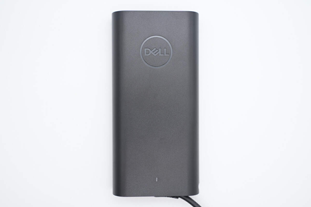
The DELL logo is on the front, and the indicator light is at the bottom.
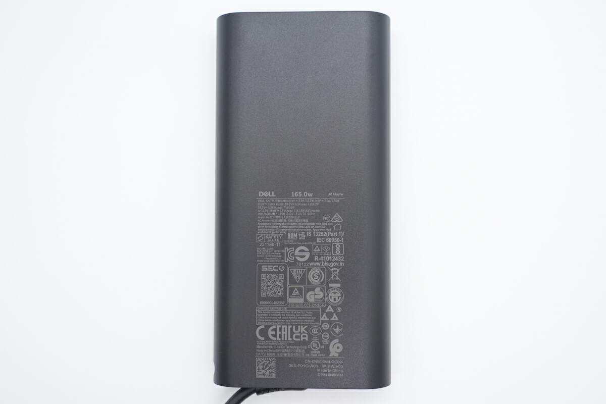
The specs info are printed on the back.
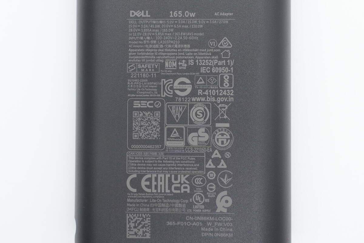
Model is LA165PM210. It can support input of 100-240V~50/60Hz 2.2A. The maximum output is 28V5.893A, which is 165W.
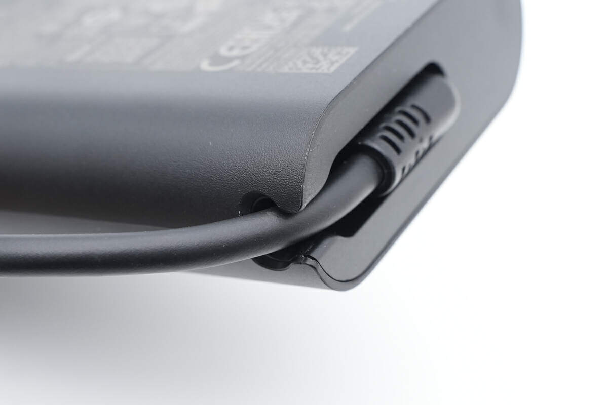
The groove near the output end can secure the USB-C cable.
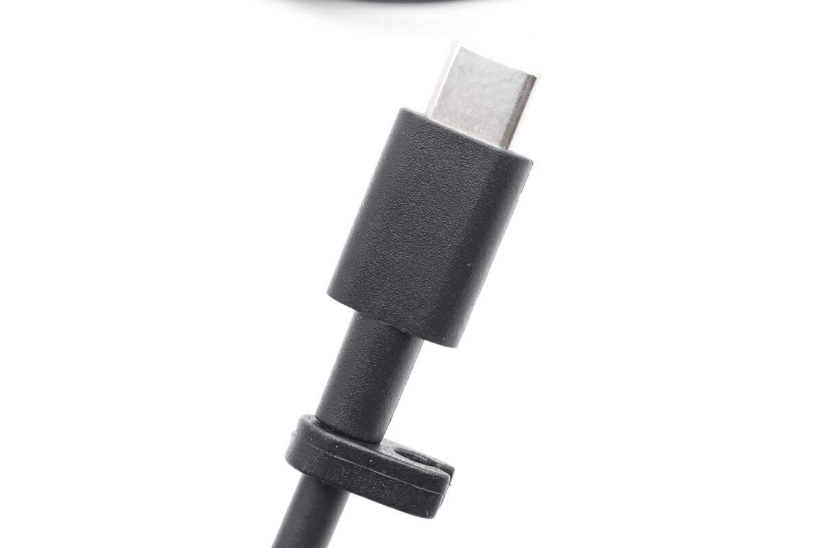
The USB-C cable has a sheath for cable management.
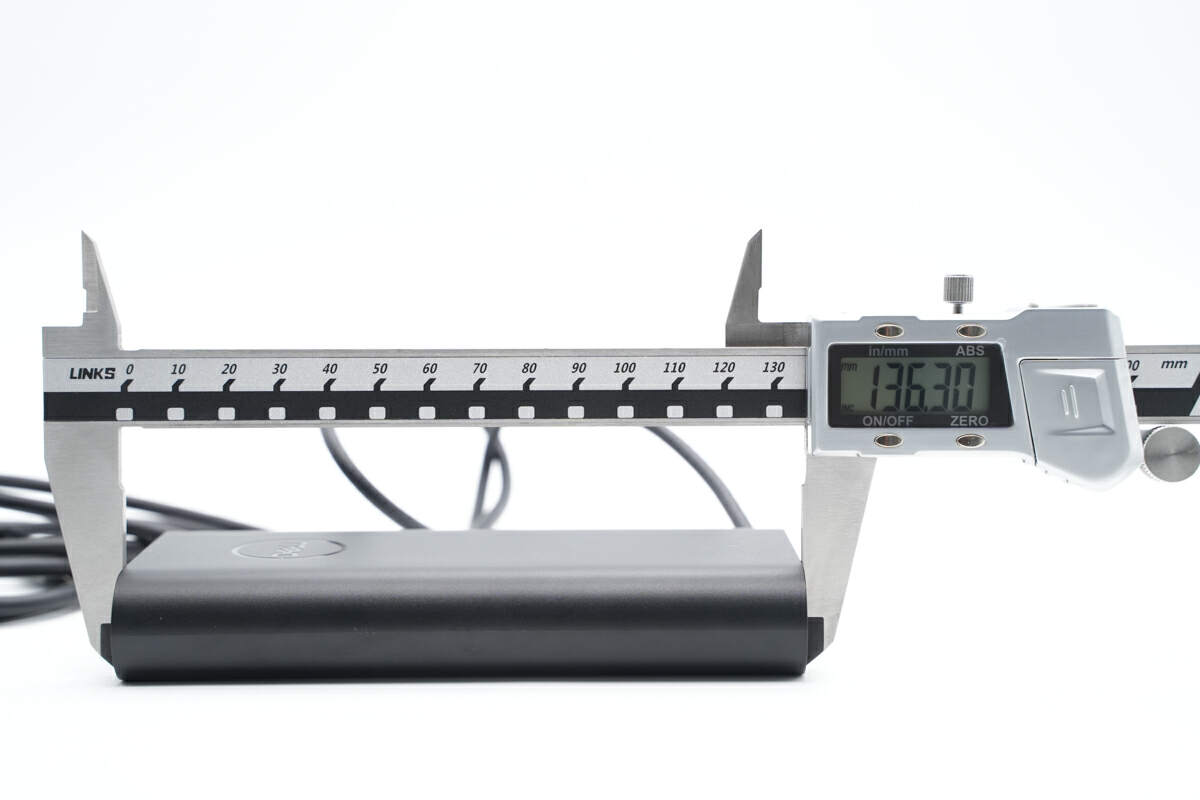
The length of the power adapter is about 136mm (5.35 inches).
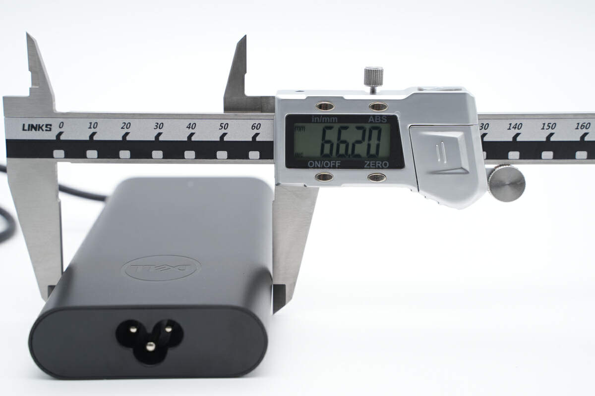
The width is about 66mm (2.6 inches).
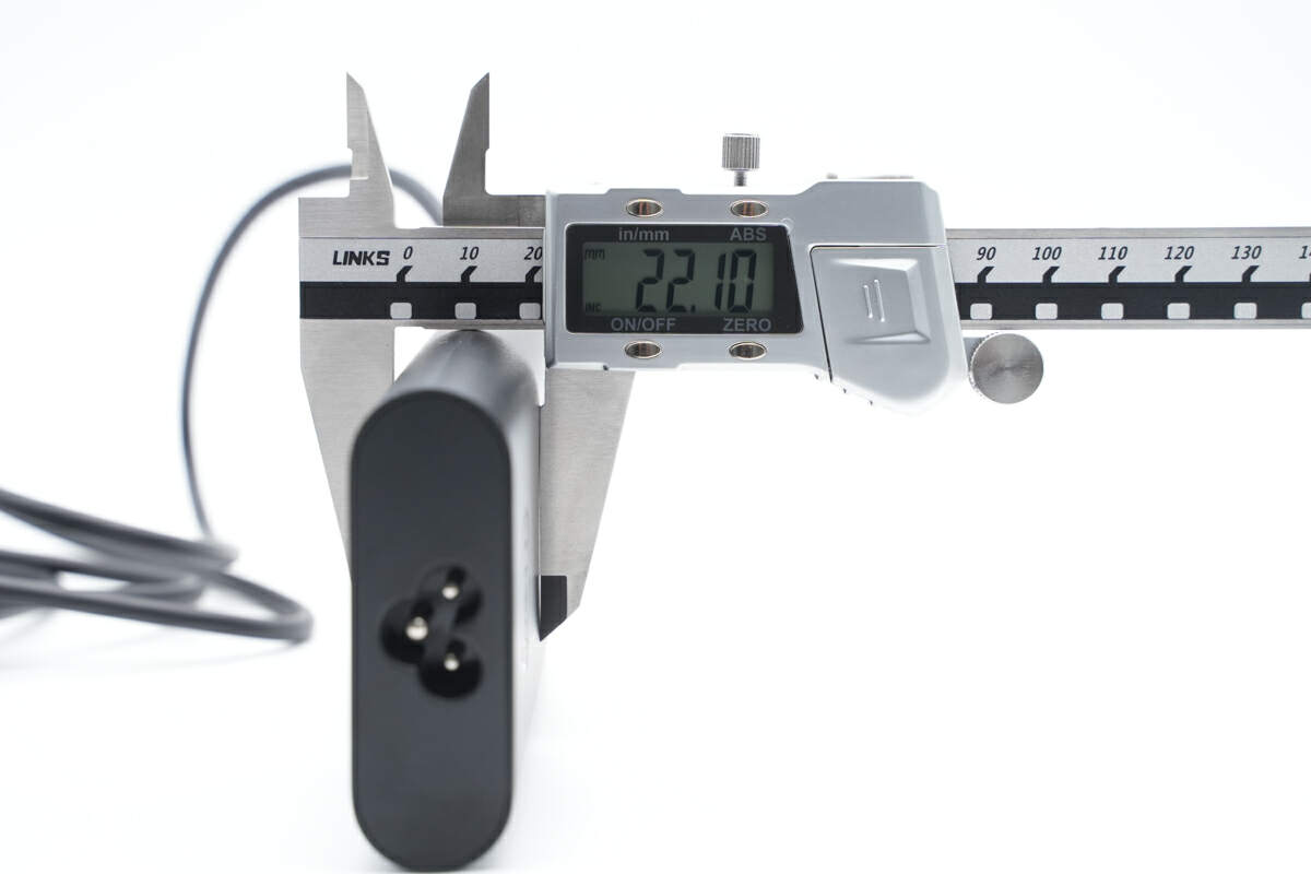
And the thickness is about 22mm (0.87 inches).
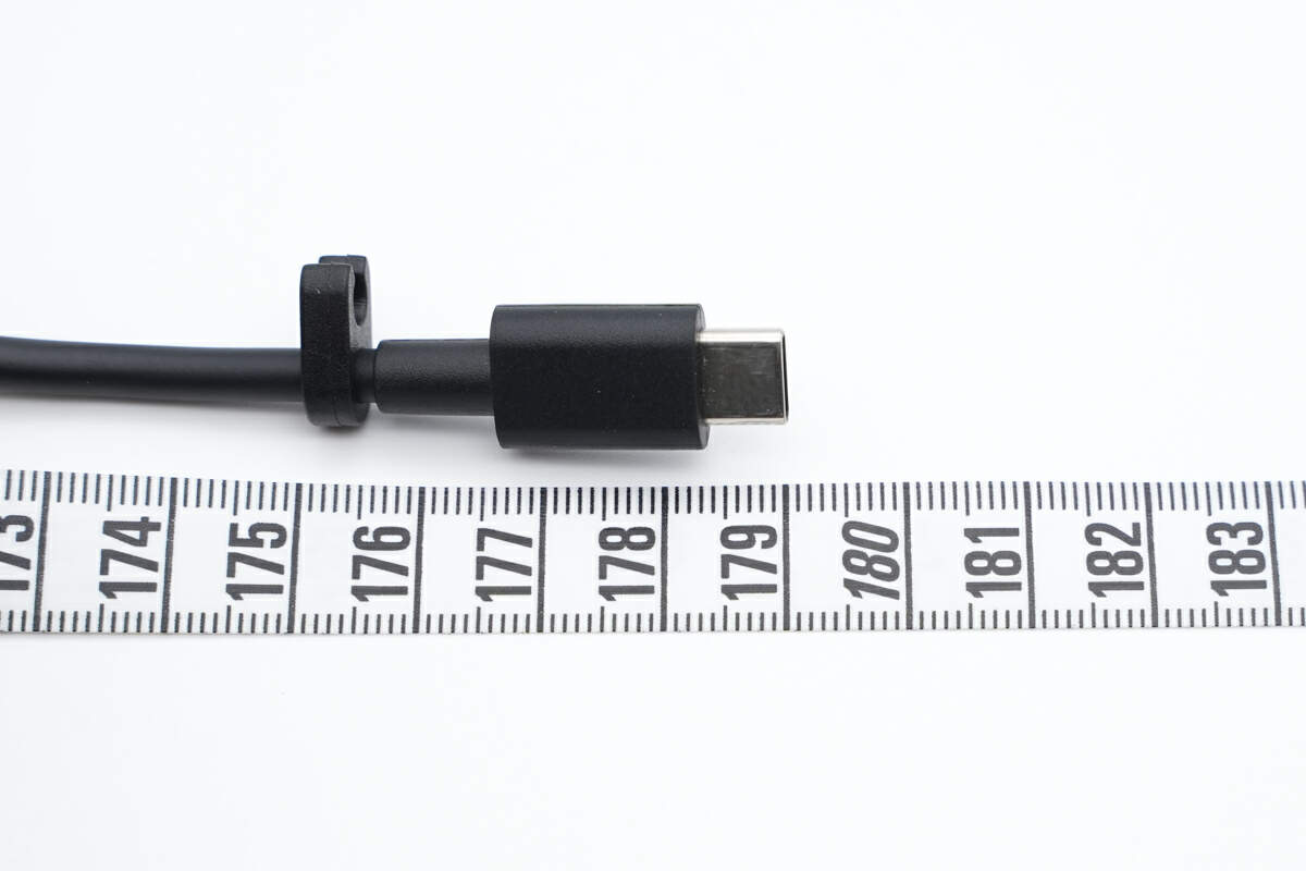
The length of the USB-C cable is about 179cm (5.87 ft).
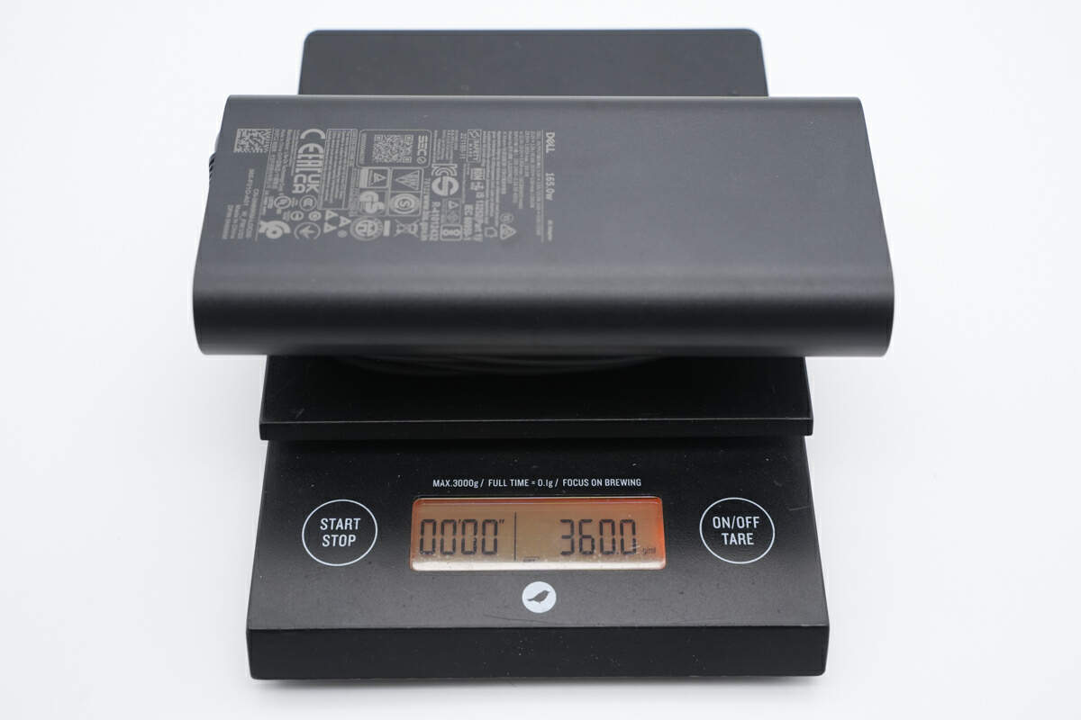
The weight of the power adapter is 360g (12.7 oz).
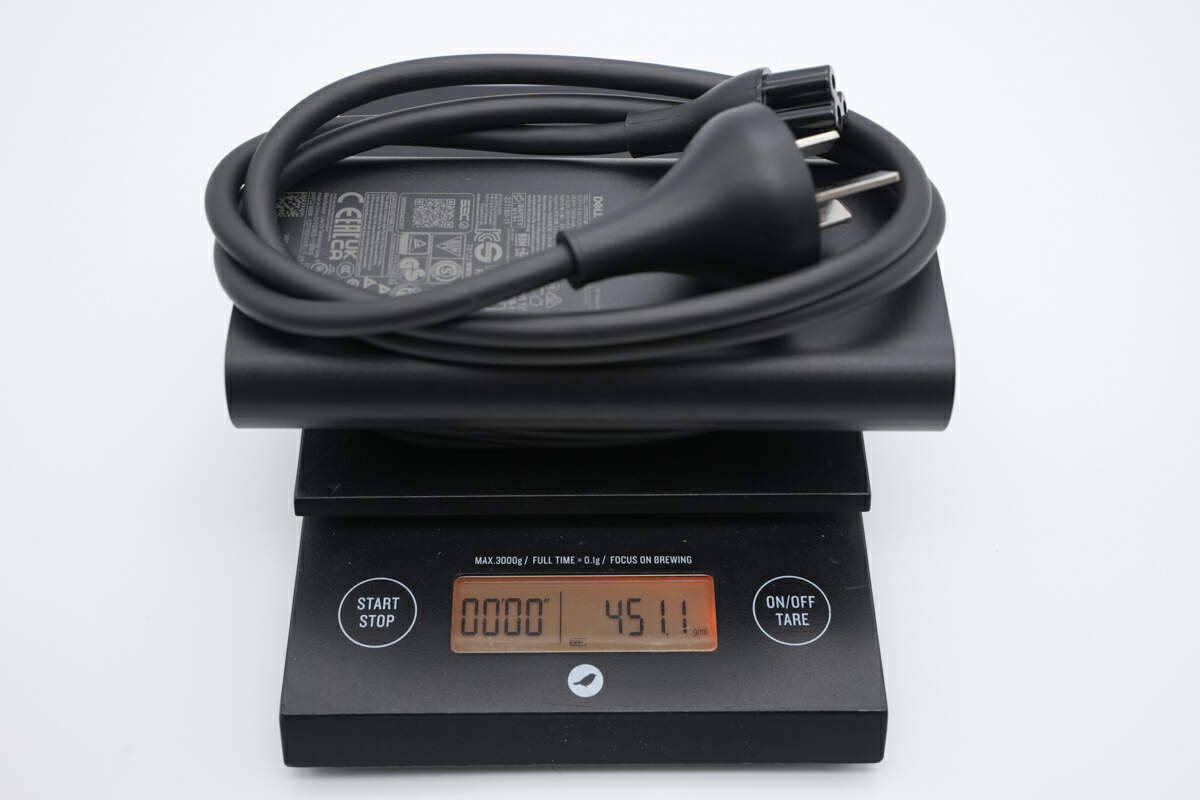
With the input cable, the weight becomes 451g (15.91 oz).
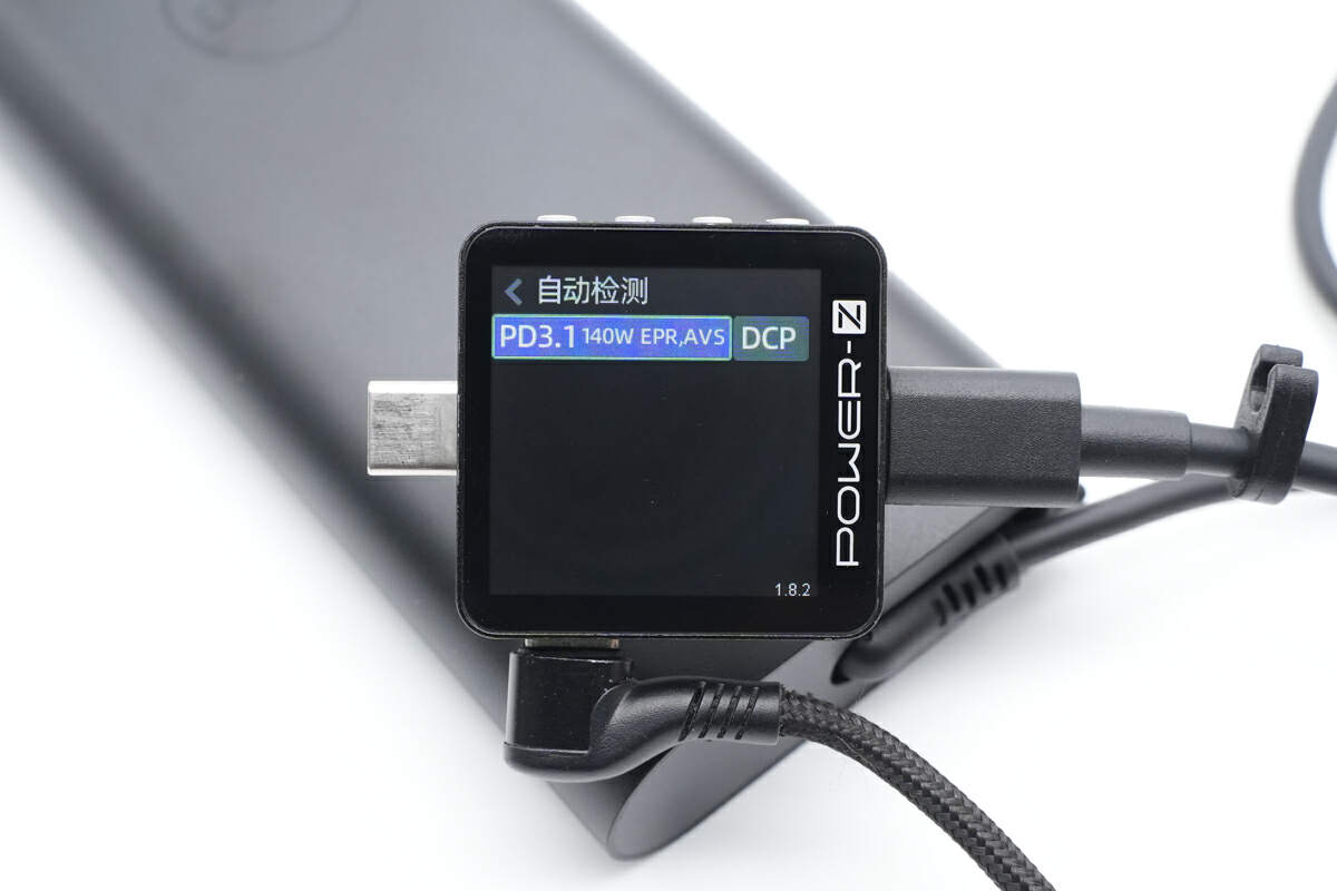
ChargerLAB POWER-Z KM003C shows it can support PD3.1 and DCP charging protocols.
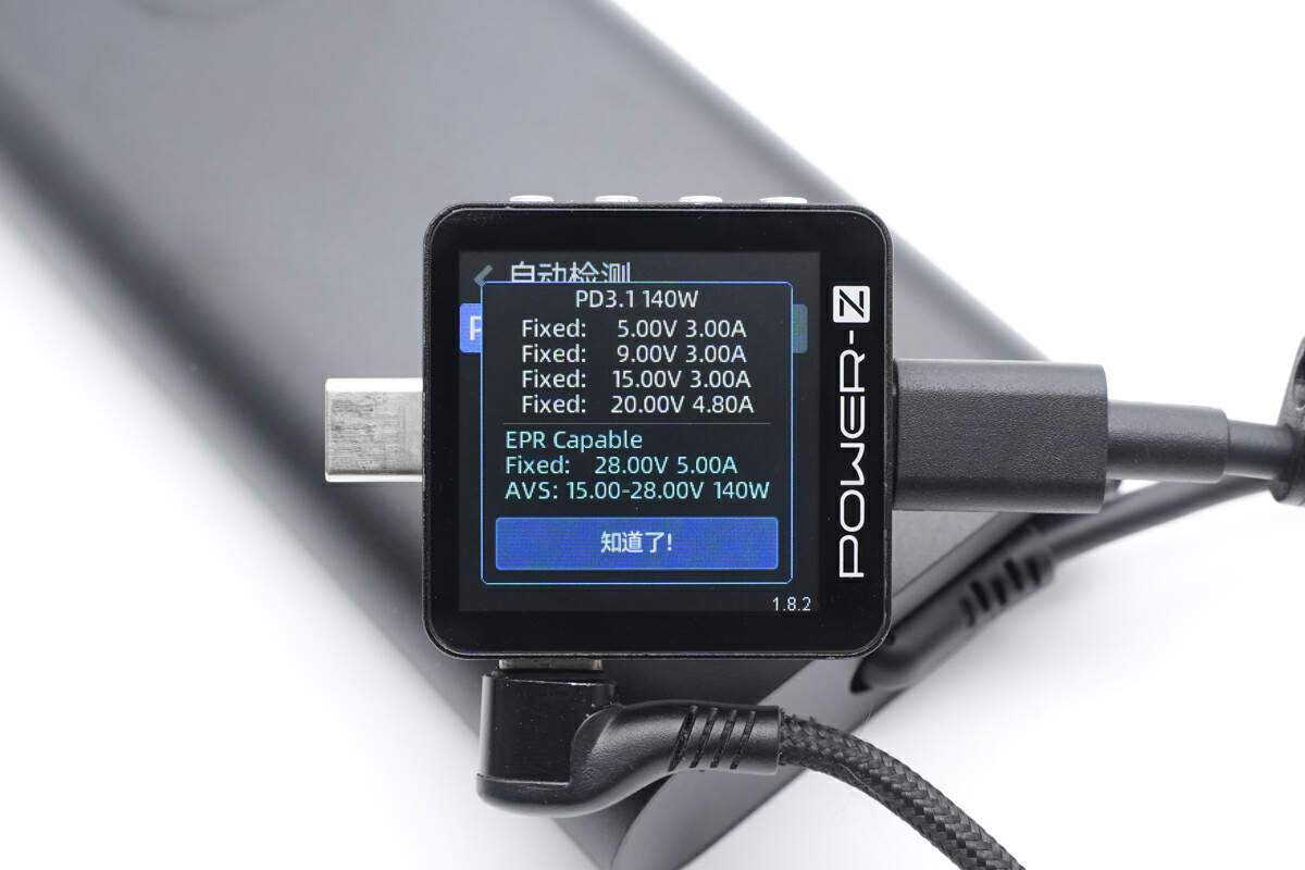
And it has five fixed PDOs of 5V3A, 9V3A, 15V3A, 20V4.8A, 28V5A, and a set of AVS, which is 15-28V 140W.
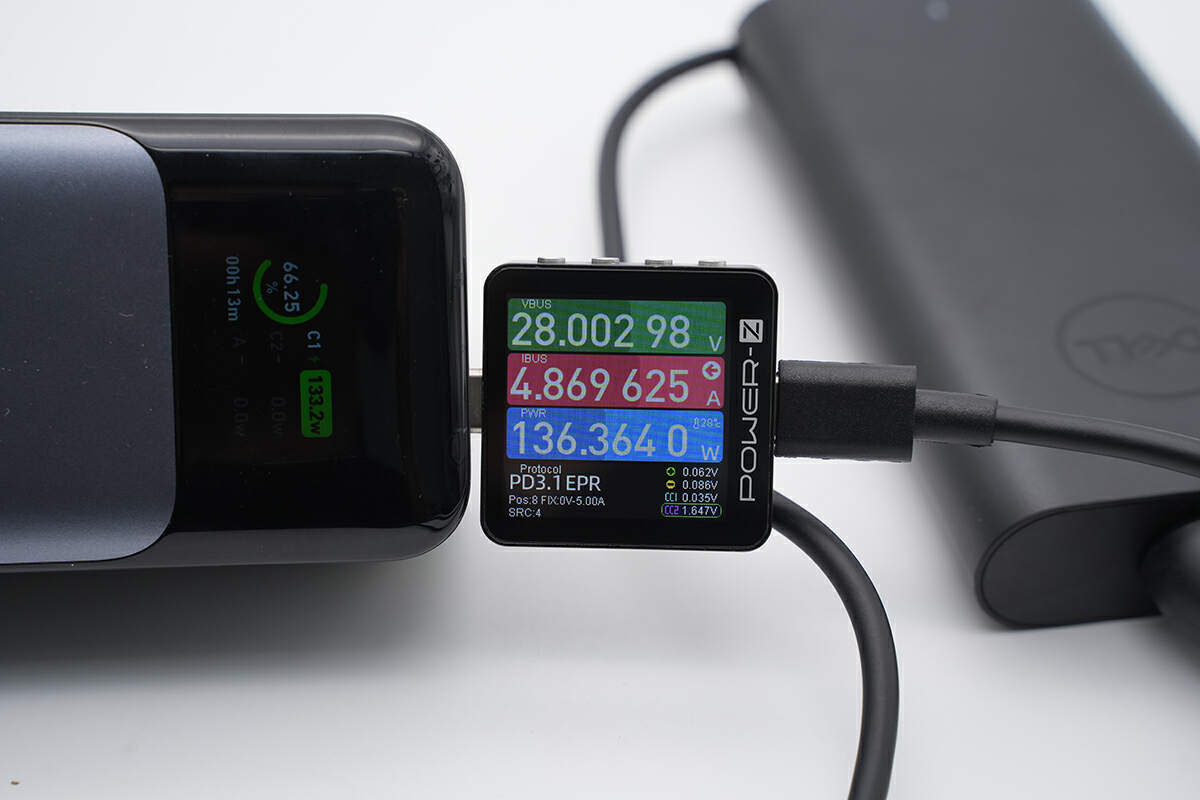
The power is 28V4.87A 136.36W when charging the Anker 140W power bank.
Teardown
Now comes the exciting part - the teardown.
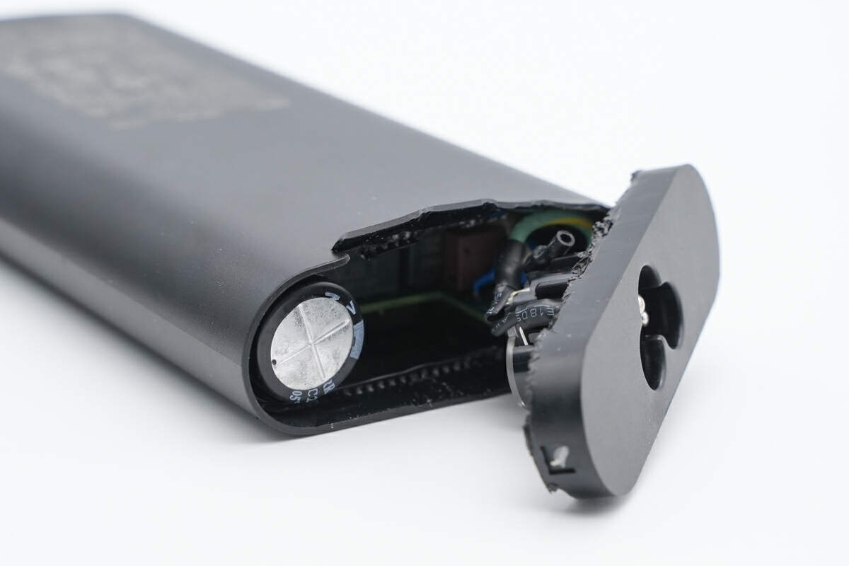
First, pry off the cover of the input end.
The transparent plastic plate is used to insulate the socket, and the solder joints are insulated by heat-shrinkable tubing.
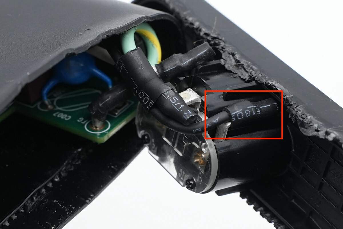
Then, cut off the input wires and take out the PCBA module.
The input wires are soldered to the PCBA and insulated by heat-shrinkable tubing.
The output wires are the same design.
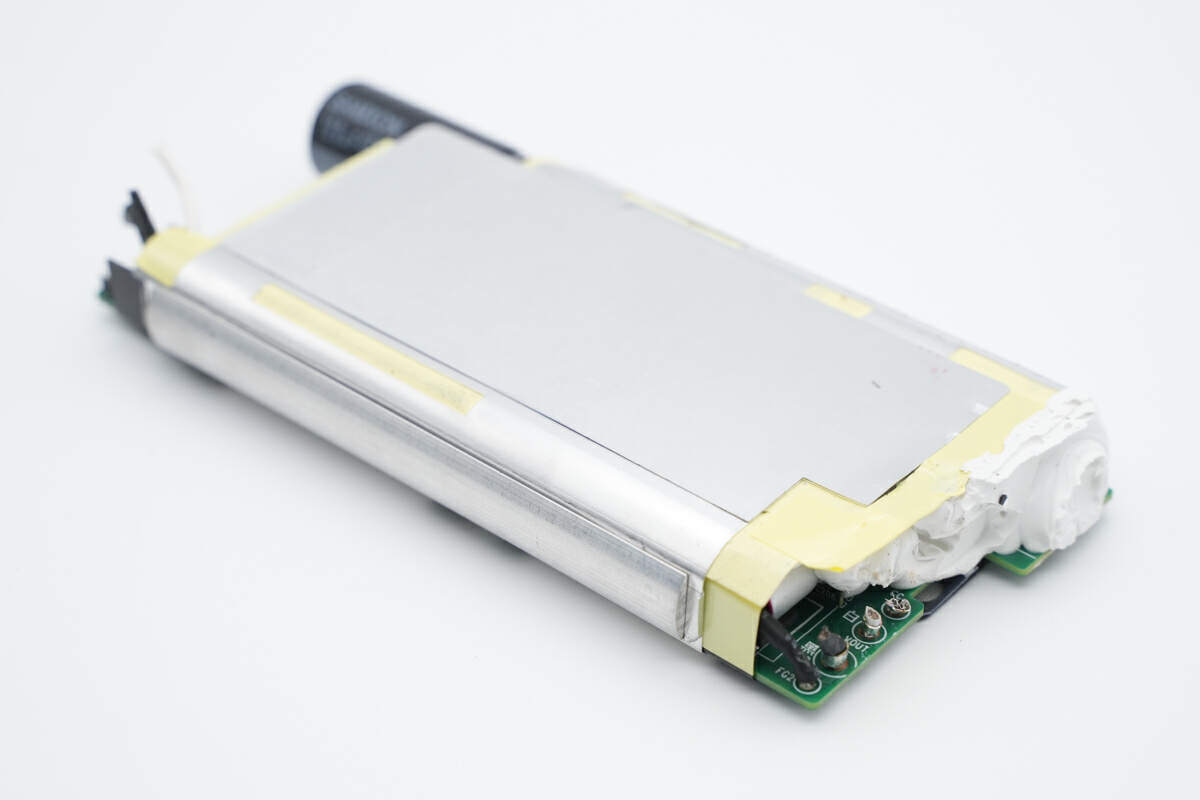
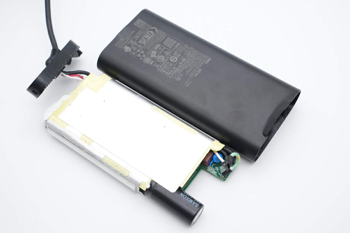
The PCBA module is pasted with an aluminum sheet.
There is another aluminum sheet below it, all of which can help dissipate heat.
The aluminum sheets are soldered to the back of the PCBA and insulated by mylar sheet.
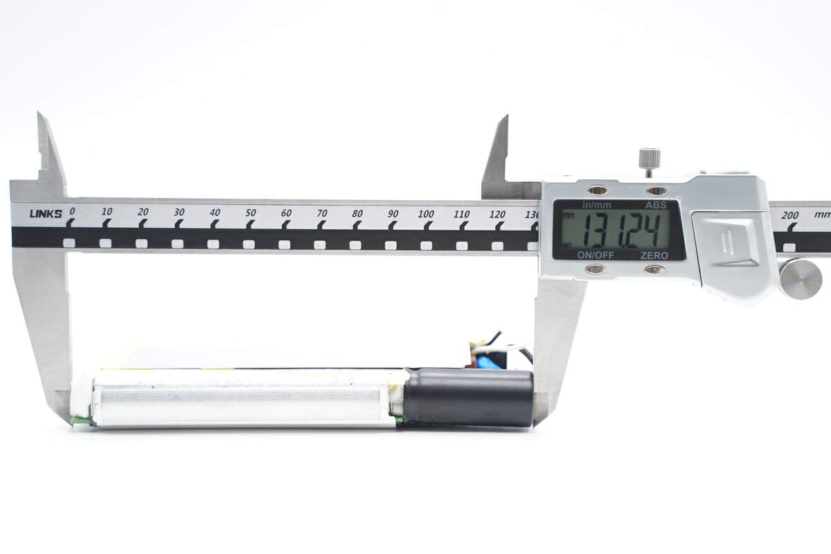
The length of the PCBA module is about 131mm (5.16 inches).
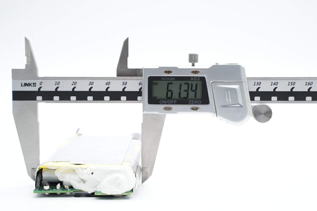
The width is about 61mm (2.4 inches).
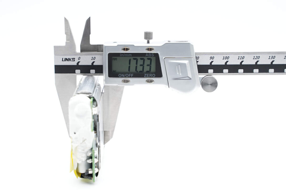
And the thickness is about 17mm (0.67 inches).
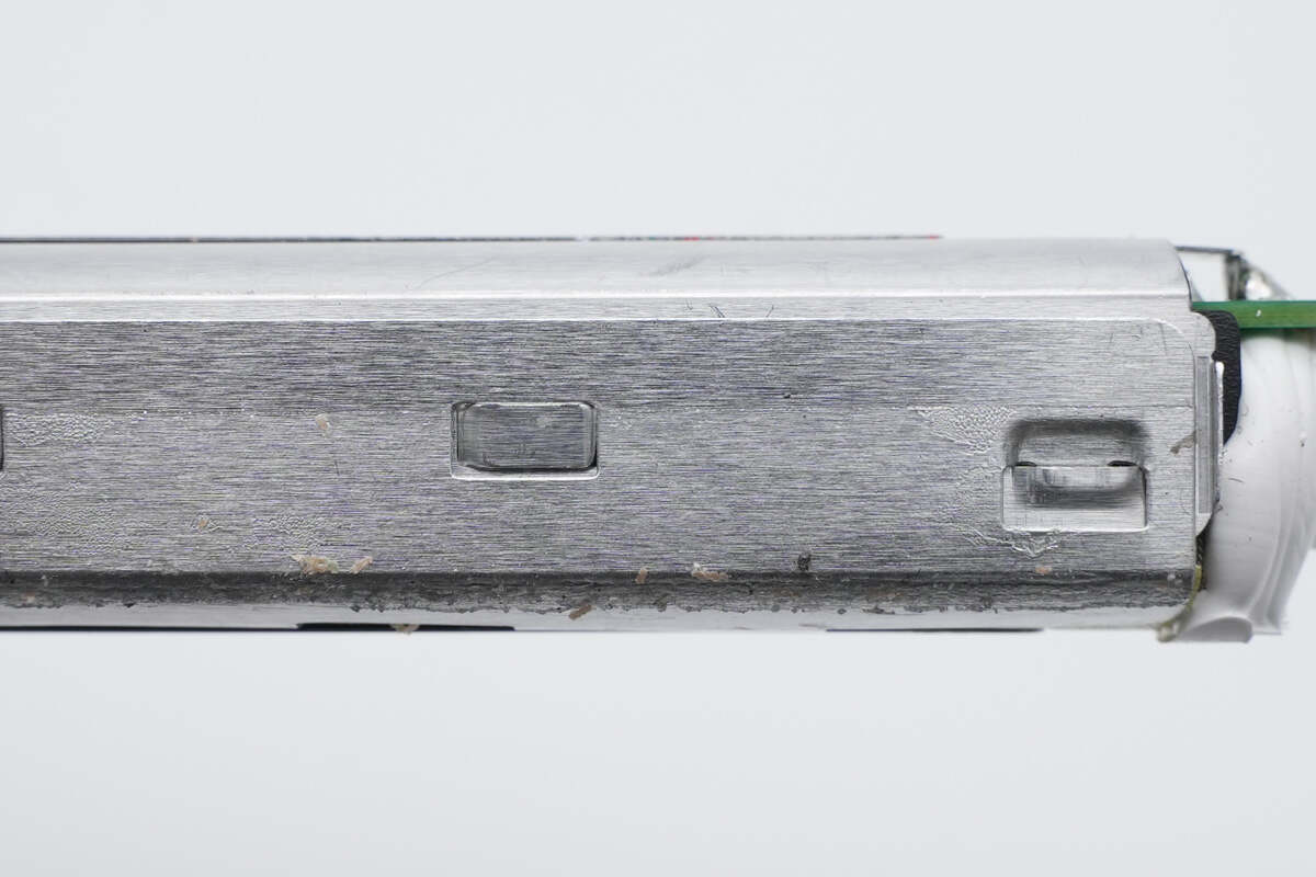
The aluminum sheets are fixed with buckles.
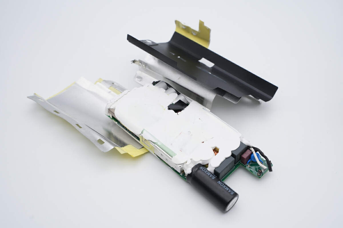
Let's remove the aluminum sheets and mylar sheet.
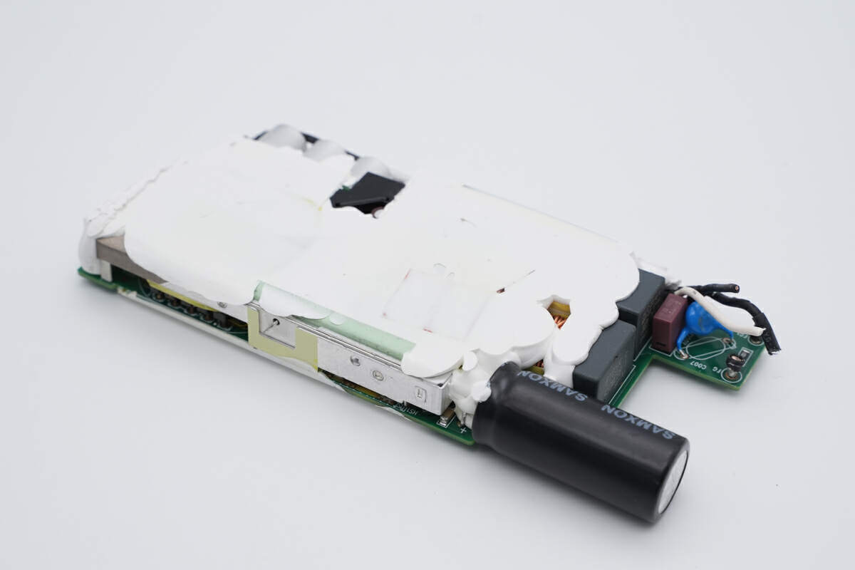
The PCBA module is filled with potting compound to enhance heat dissipation.
Same on the back.
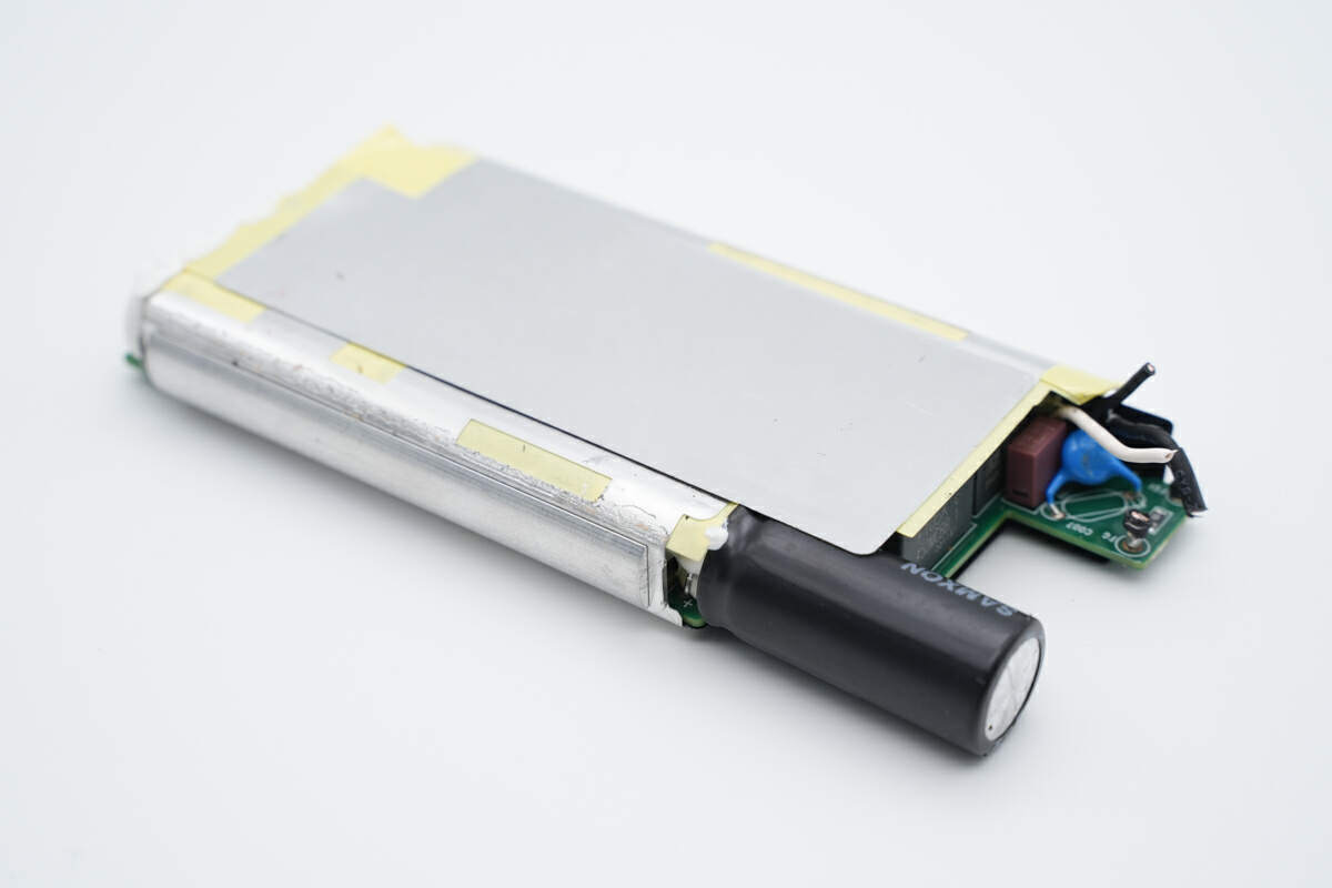
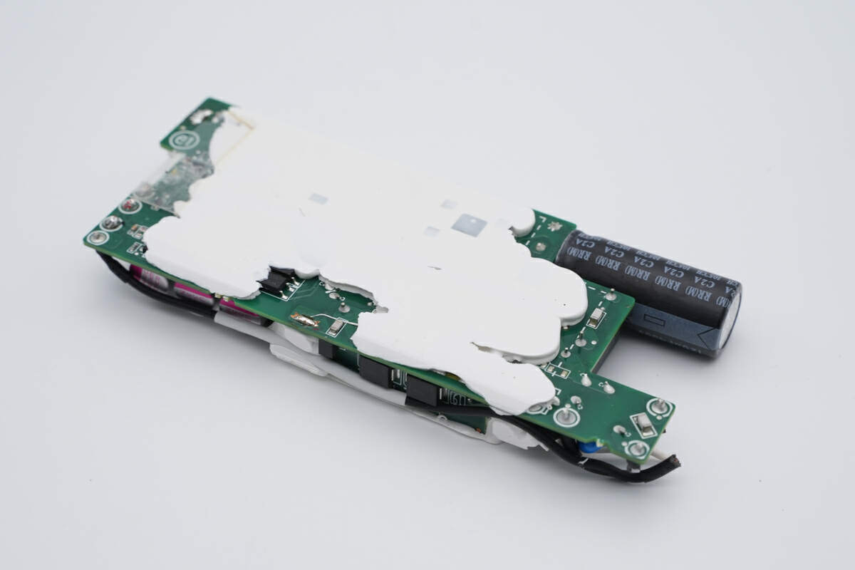
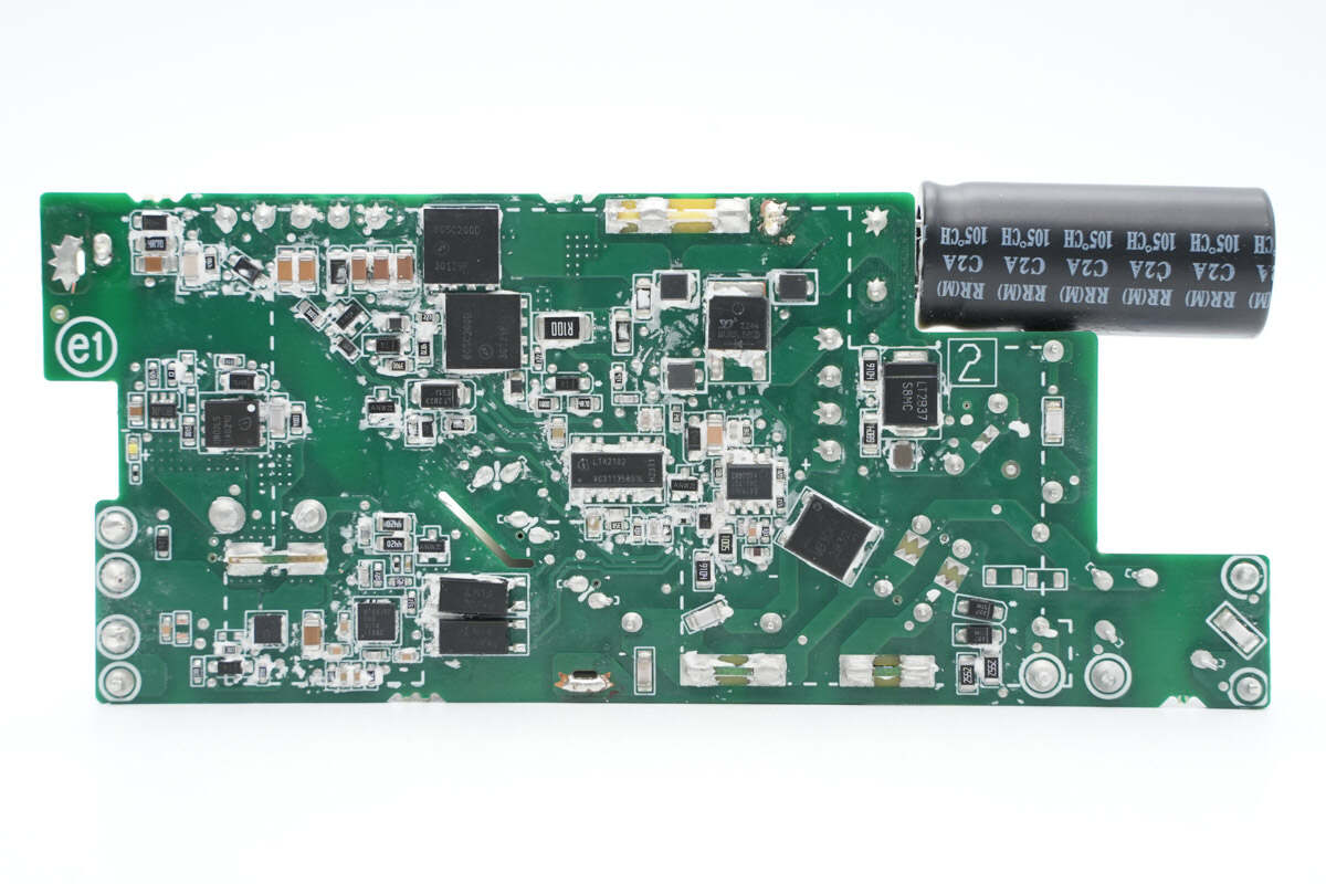
Several small PCBs are vertical soldered on the front of the PCBA module, to improve space utilization.
Here is the aluminum sheet on the other side of the PCBA.
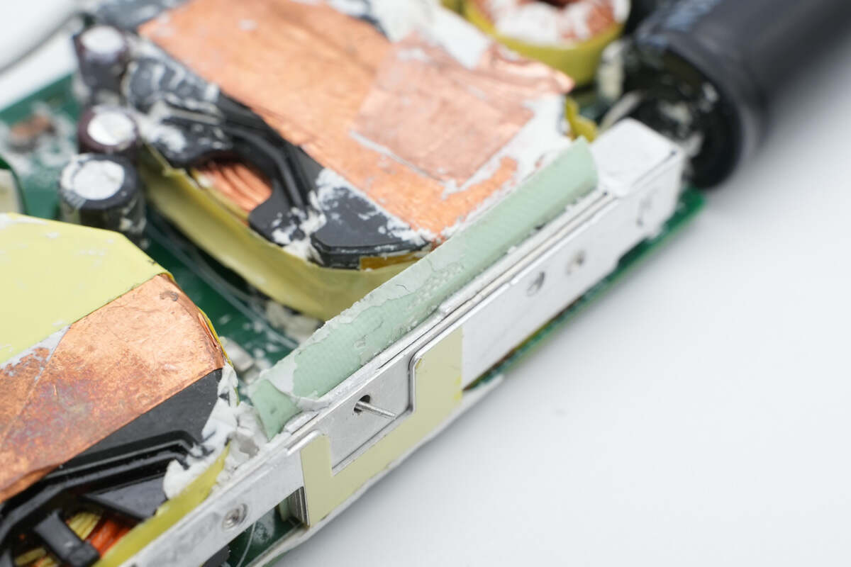
And there is a green thermal pad pasted between the small PCB and the aluminum sheet.
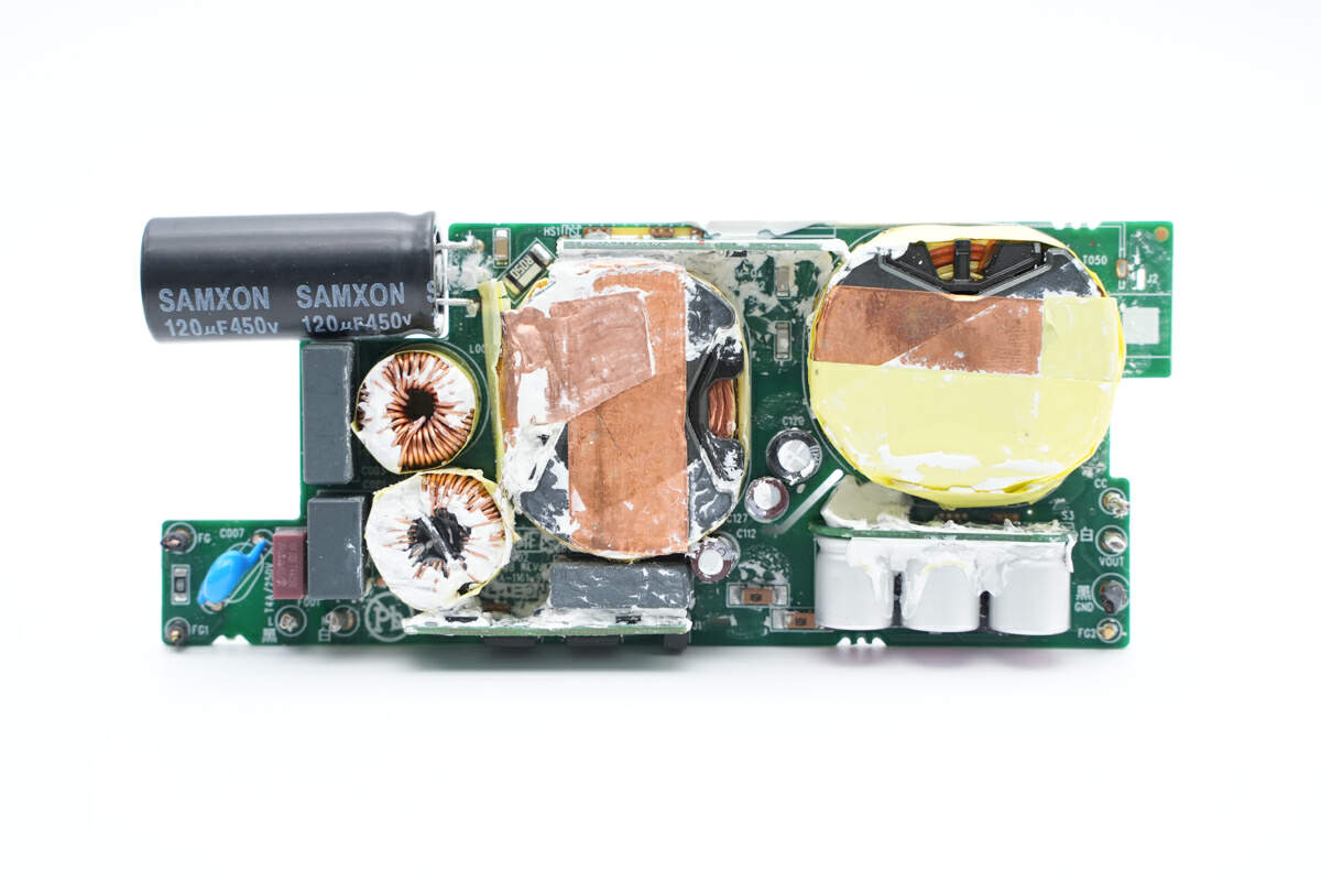
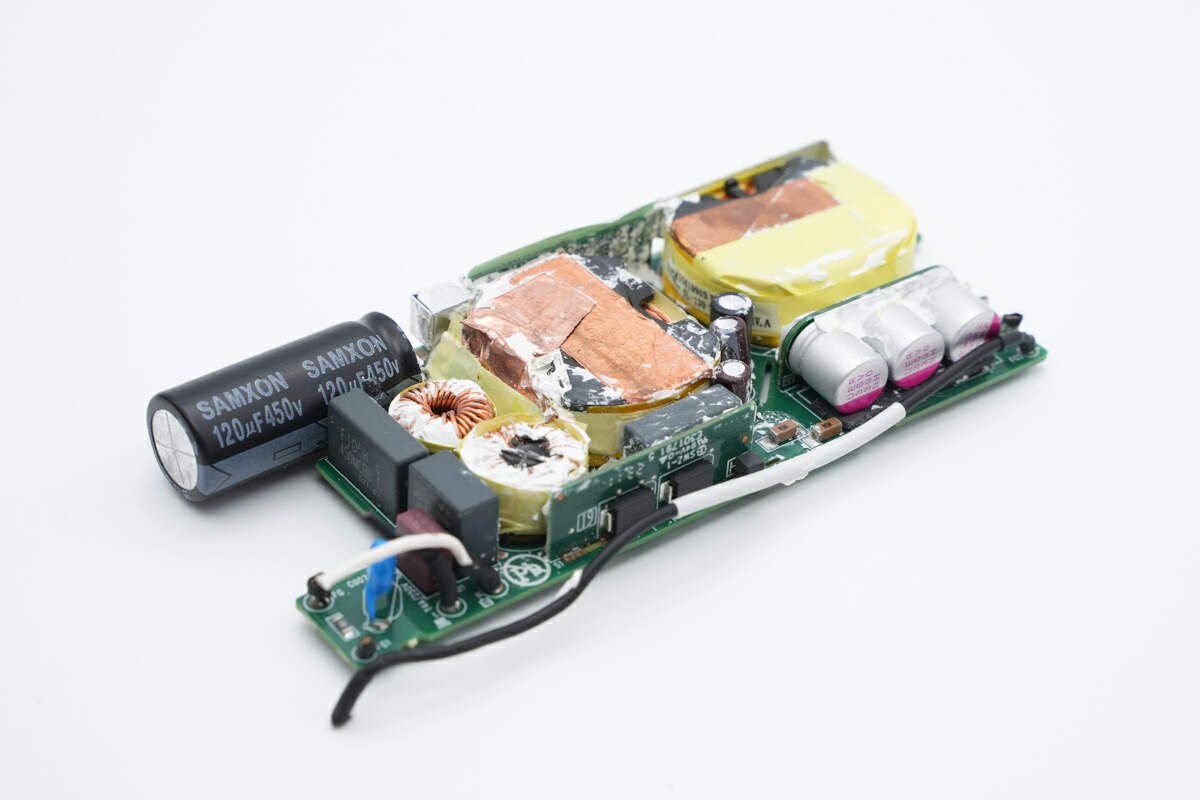
The AC input end is on the lower left corner, and the synchronous rectifier circuit is on the right side.
And there are bridge rectifier, PFC controller, PFC rectifier MOSFET, hybrid-flyback controller and half-bridge MOSFET on the back.
This power adapter adopts a half-bridge PFC+HFB circuit design with active bridge rectification. It supports synchronous rectification and can output wide-range of voltage.
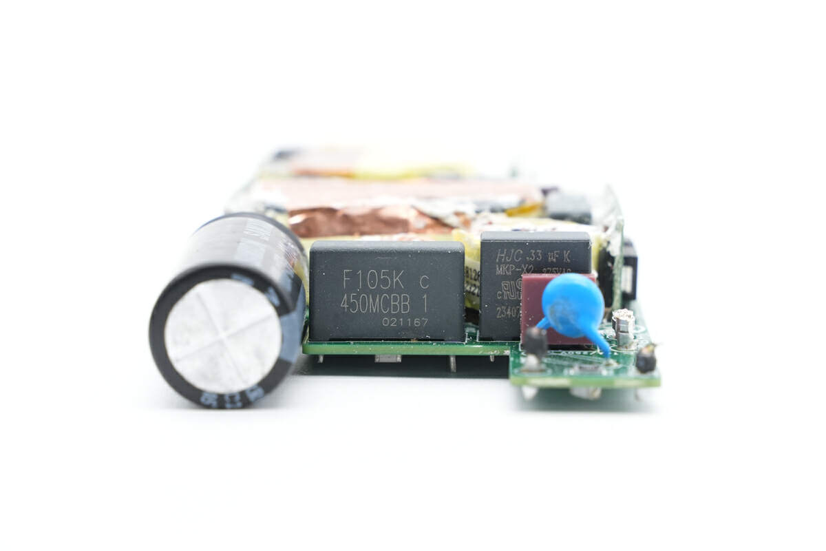
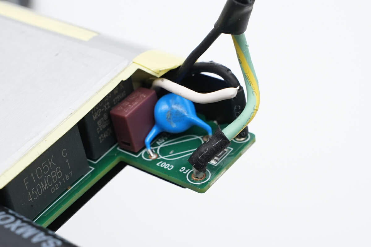
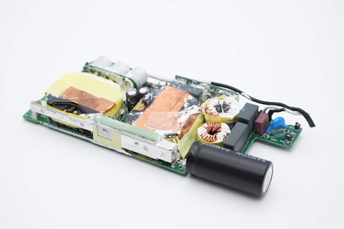
There are blue Y capacitor, fuse, safety X2 capacitor, film capacitor, and electrolytic capacitor on the input end.
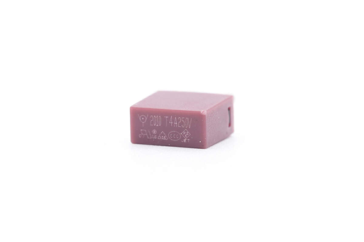
The fuse is from WalterFuse. 4A 250V.
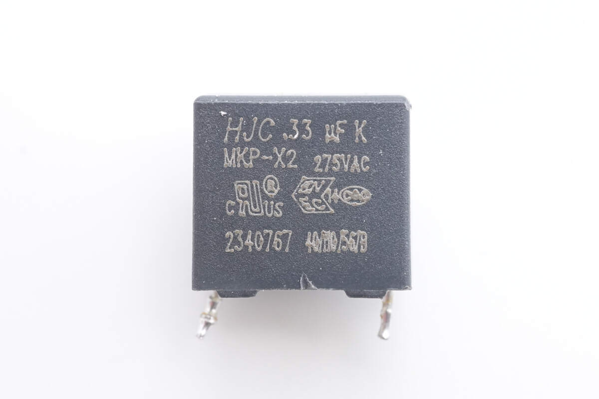
The safety X2 capacitor is from HJC. 0.33μF.
The common mode choke is wound with magnet and insulated wires, and it's insulated with bakelite.
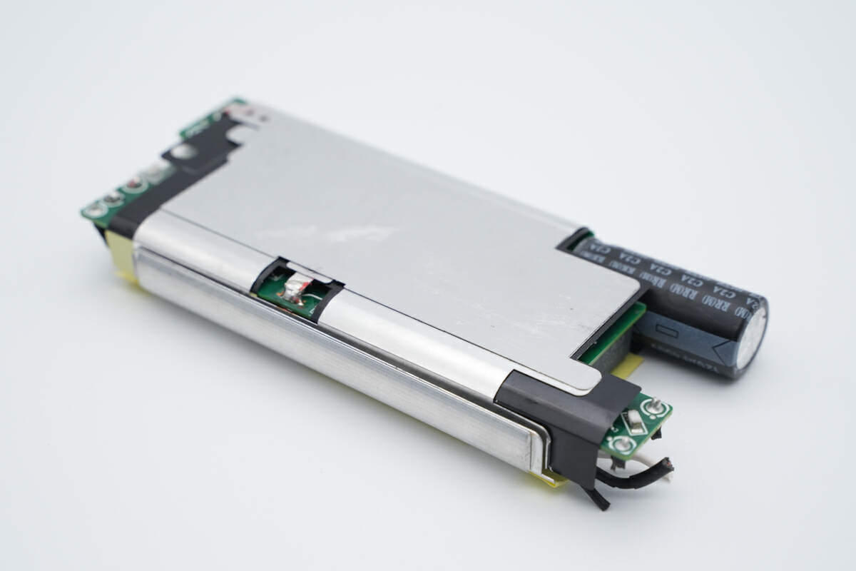
The active rectifier PCB and filter capacitor PCB are on the side of the main PCBA.
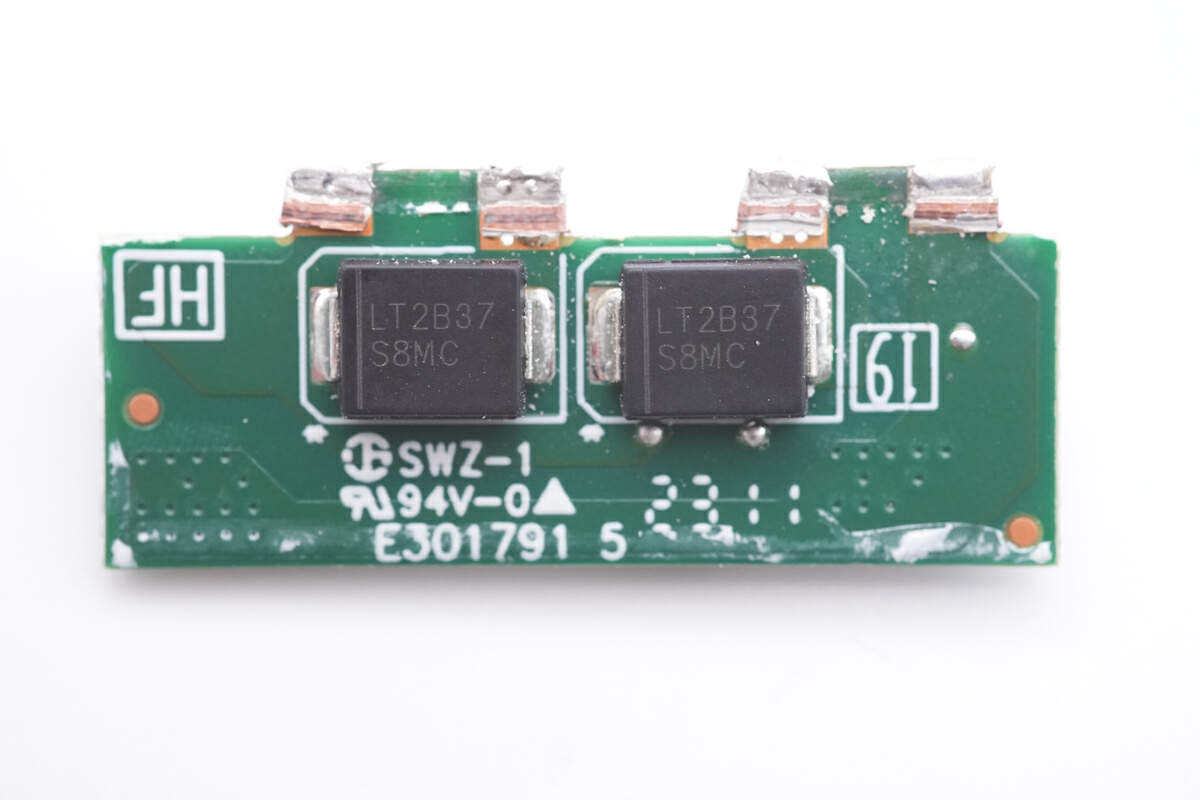
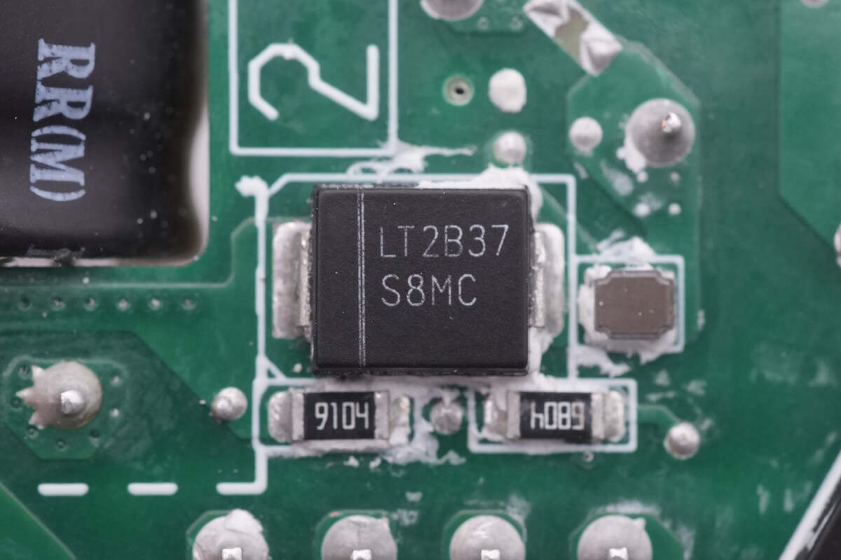
These two rectifier MOSFETs on the active rectifier PCB are from LITEON. Model is S8MC. 8A 1000V.
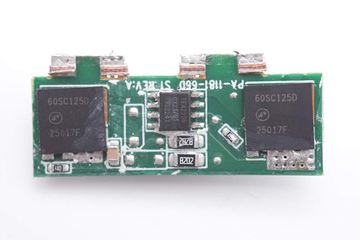
The active bridge rectifier controller and rectifier MOSFET are on the back of it.
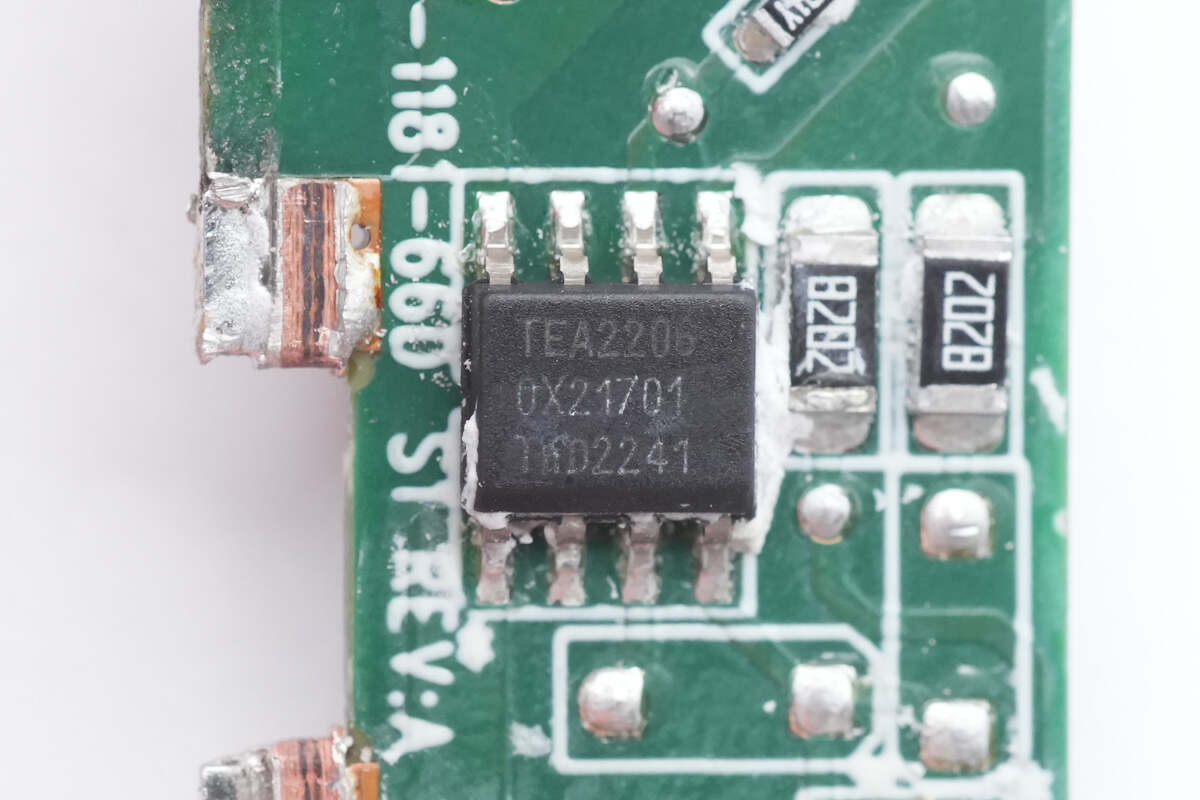
The active bridge rectifier controller is from NXP, and it uses two NMOSs to reduce the loss caused by the forward voltage drop of the diode by half. Model is TEA2206.
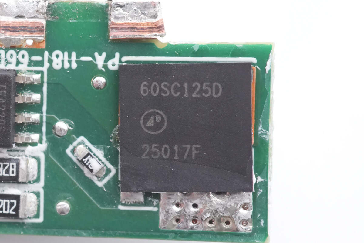
The rectifier MOSFET is from APEC. It adopts PDFN8 x 8_HV package. Model is AP60SC125DDT8. 600V 125mΩ.
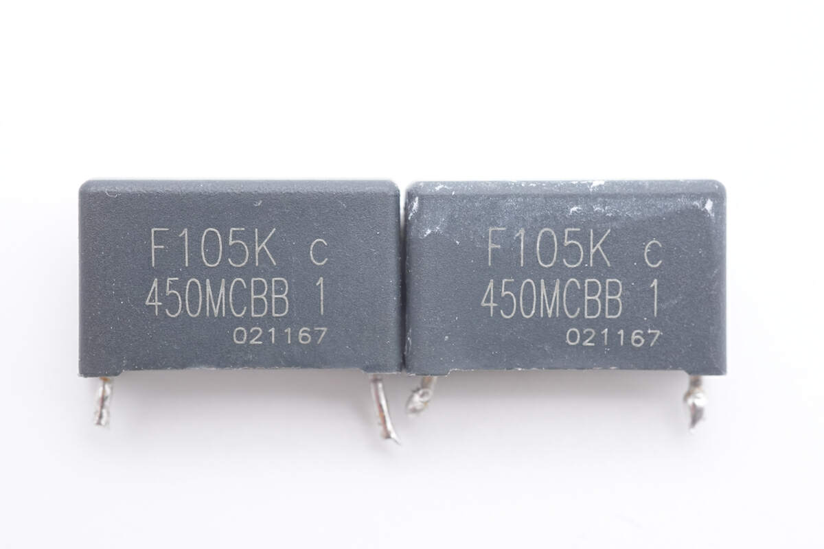
These two film capacitors are 1μF 450V.
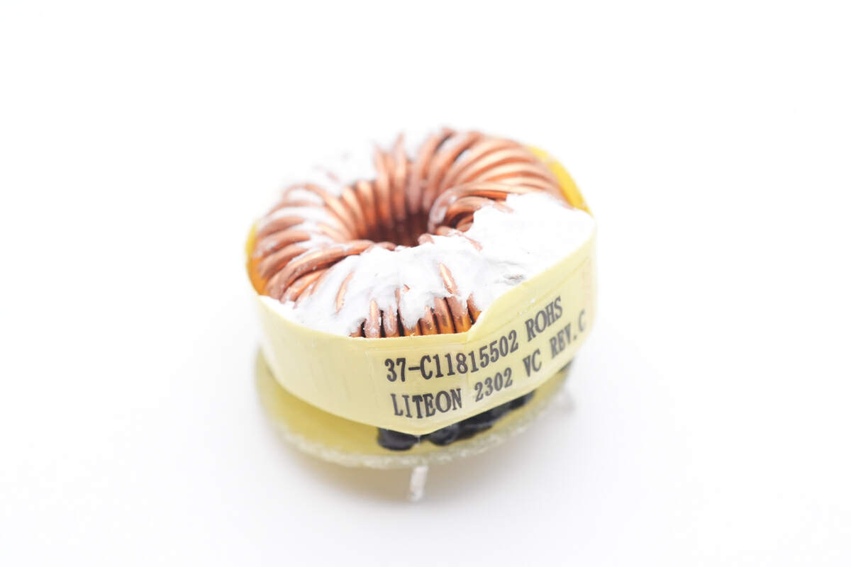
Another common mode choke is wound with magnet and insulated wires, and it's also insulated with bakelite.
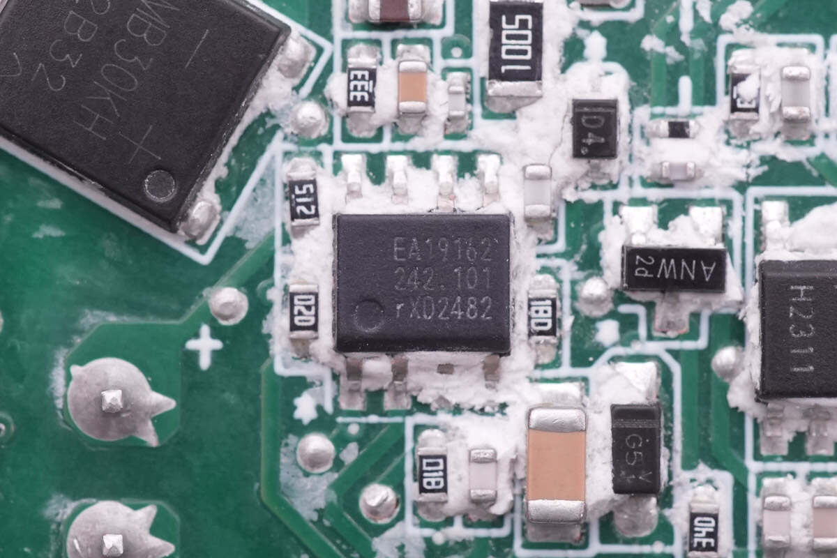
The PFC controller is also from NXP. It can boost the rectified voltage and correct active power factor. Model is TEA19162.
The PFC MOSFET is on the side of the PCBA module, and the electrolytic capacitor for input filtering is on the right.
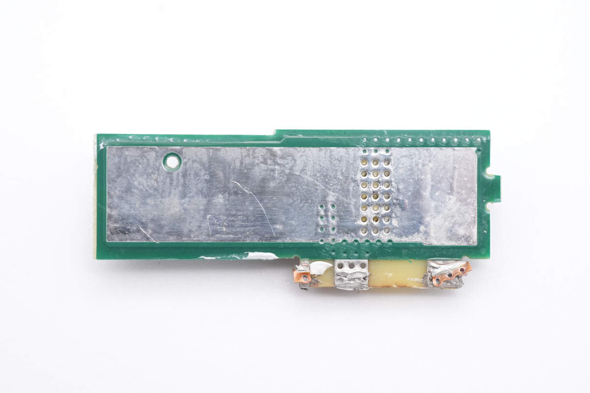
This small PCB has many small holes for heat dissipation.
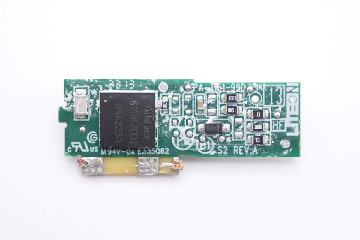
The PFC MOSFET is on the back.
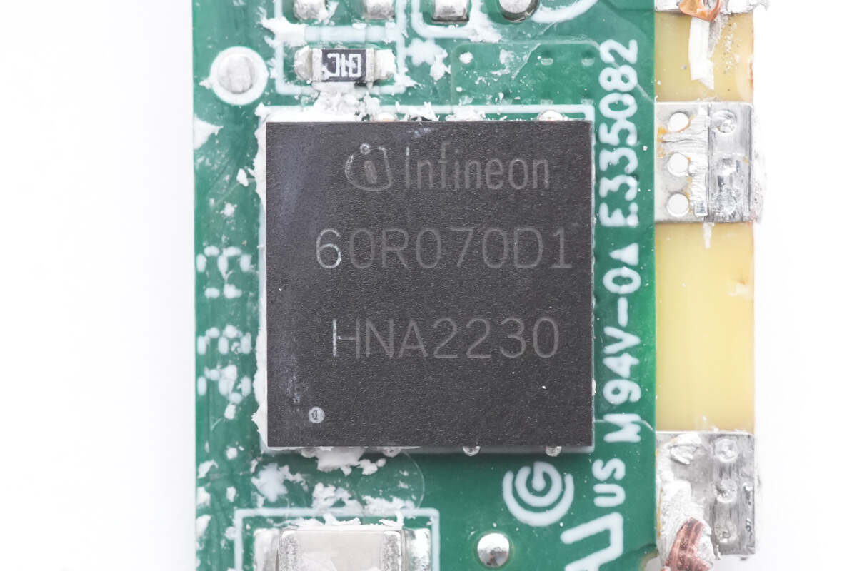
The PFC MOSFET is from Infineon, and it adopts PG-LSON-8-1 package. Model is IGLD60R070D1. 600V 70mΩ.
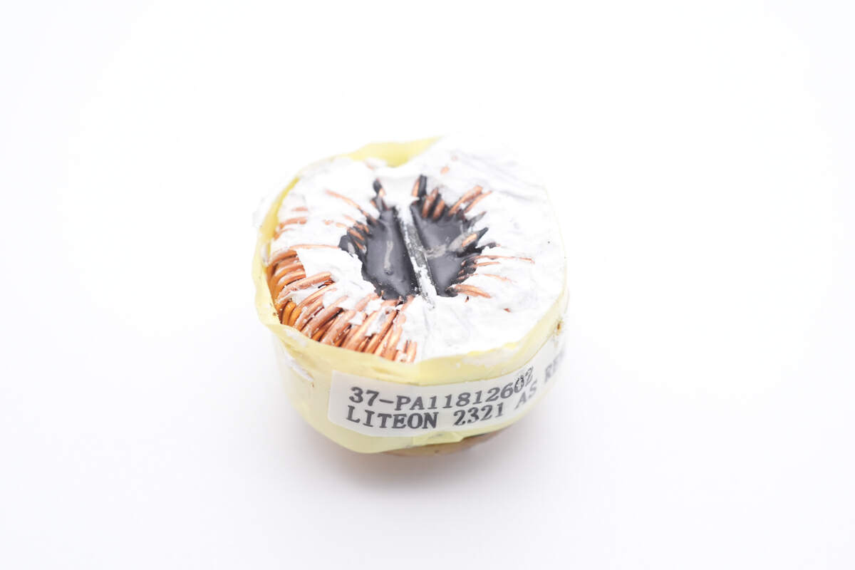
The PFC boost inductor is wrapped in copper foil.
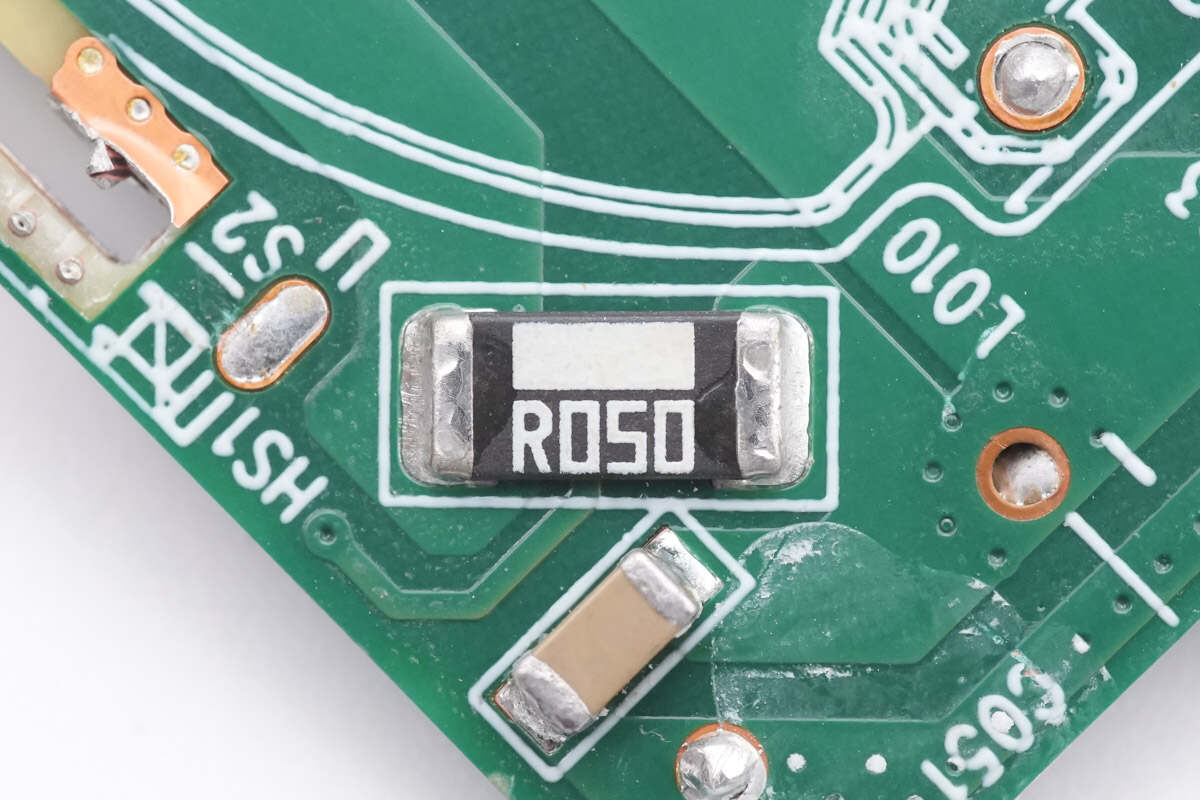
The 50mΩ resistor is used to detect the current of the PFC MOSFET.
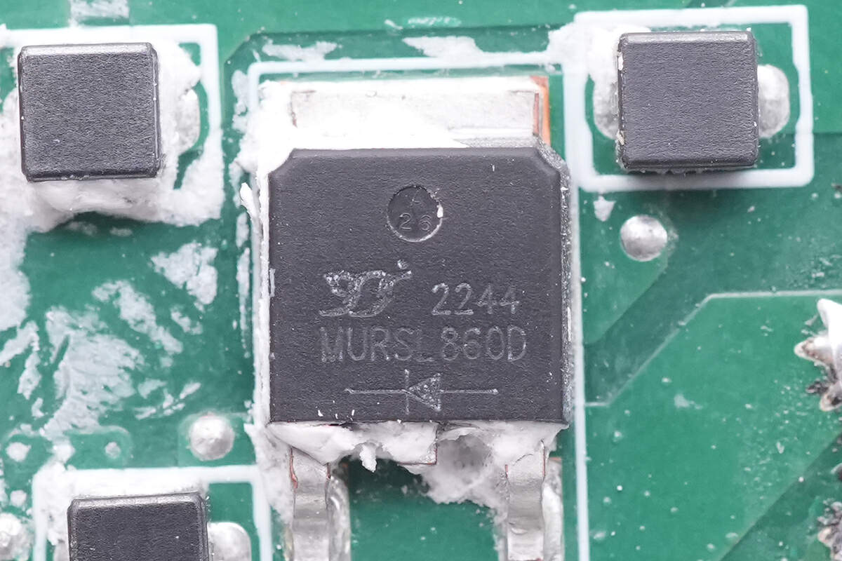
The PFC rectifier MOSFET is from Yangjie, and it adopts TO252 package. It can do ultra-fast recovery. Model is MURSL860D. 600V 8A.
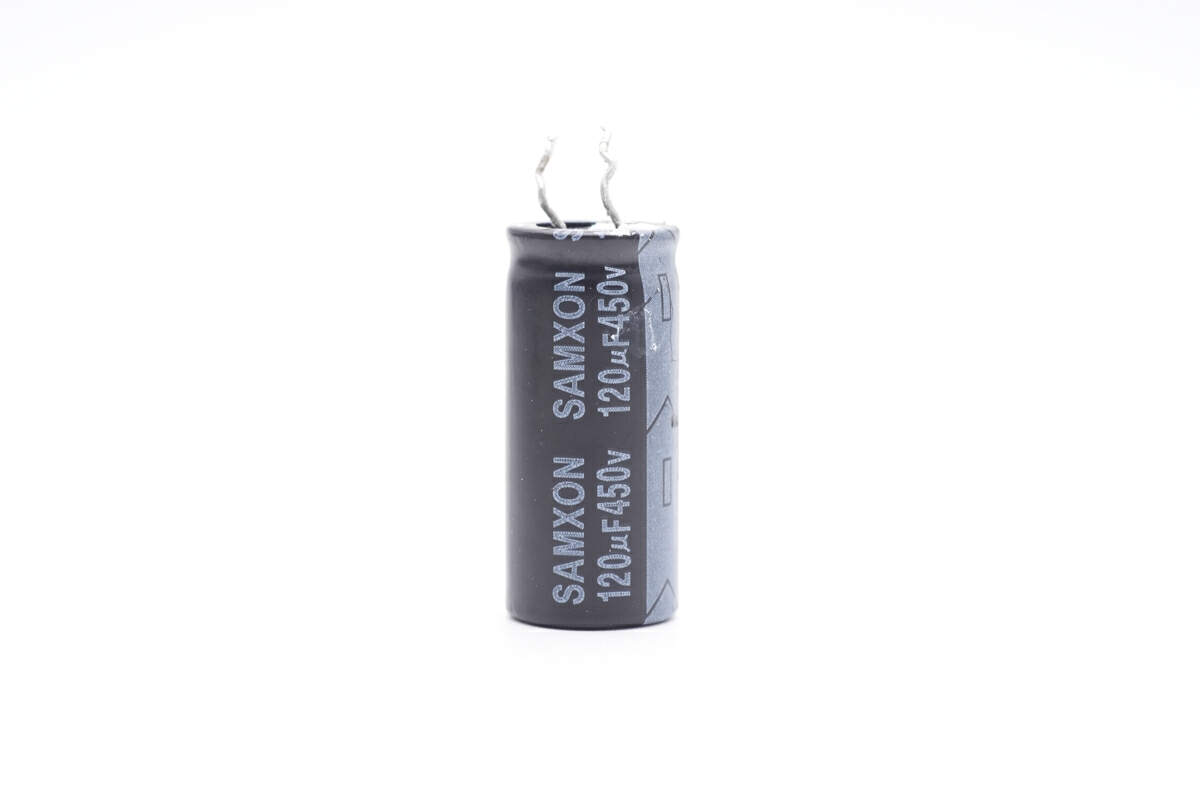
The electrolytic capacitor for input filtering is from SAMXON. 120μF450V.
The S8MC diode is used for the PFC bypass and charges the electrolytic capacitor.
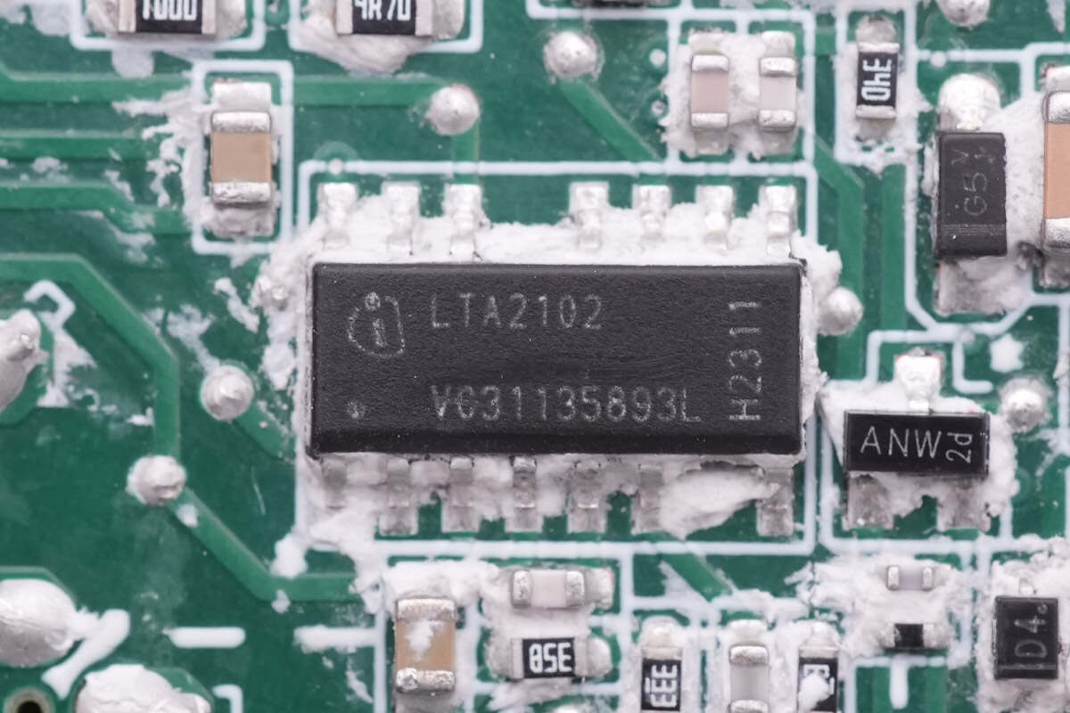
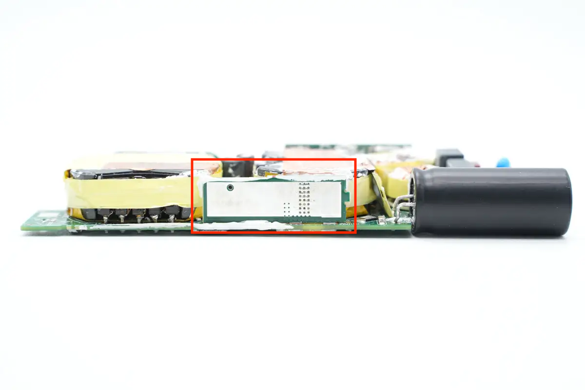
The master control chip is from Infineon and is marked with LTA2102.
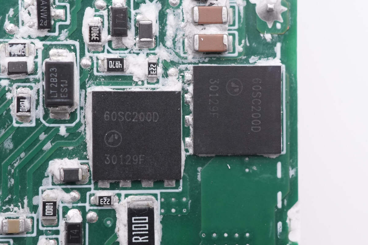
These two half-bridge MOSFETs are also from APEC, and they adopt the PDFN8 x 8_HV package. Model is AP60SC200DDT8. 600V 200mΩ
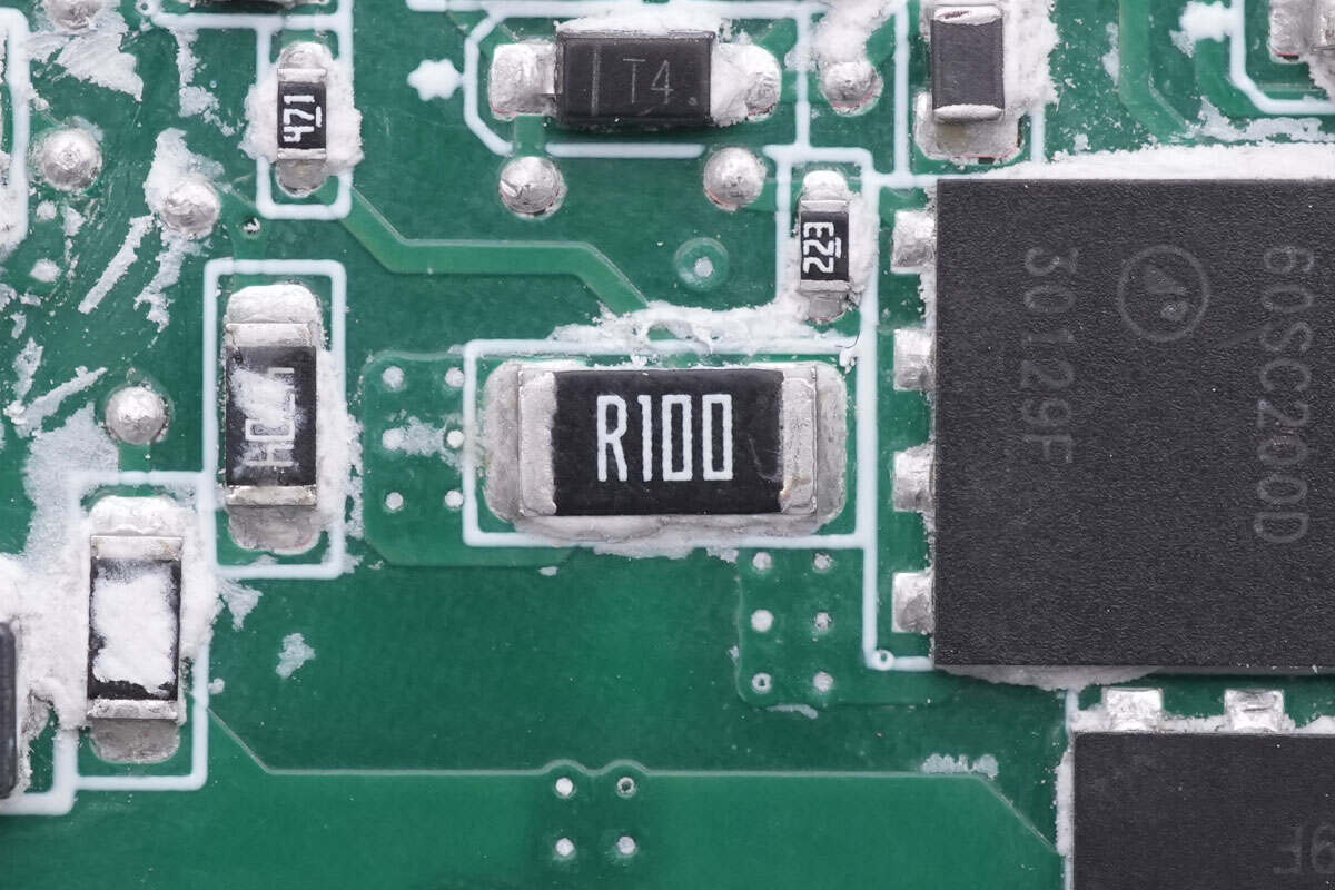
The 100mΩ resistor is used to detect the MOSFET current.
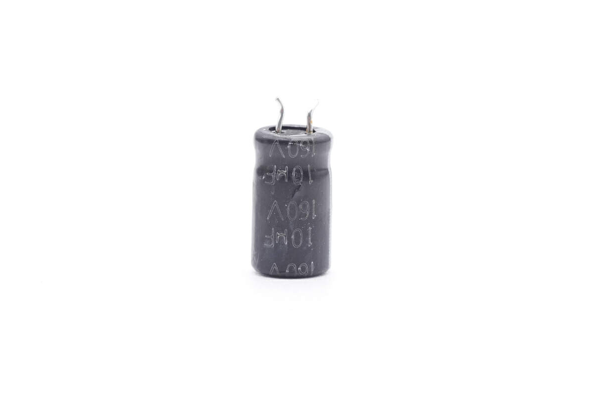
The electrolytic capacitor that powers the master control chip is from Elite. 10μF 160V.
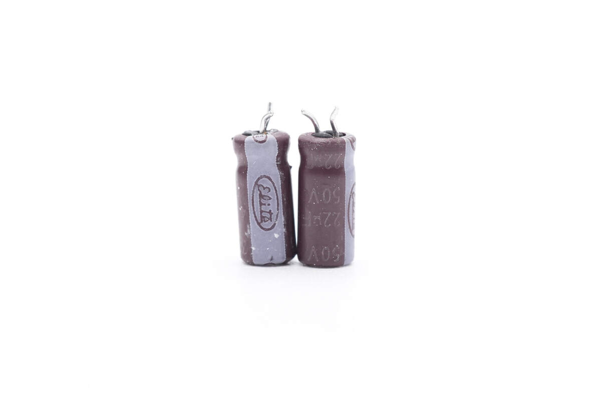
The other two electrolytic capacitors are 22μF 50V.
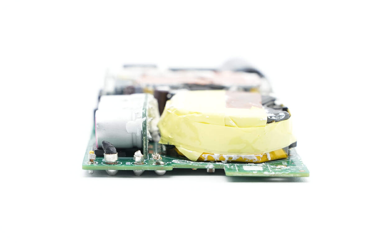
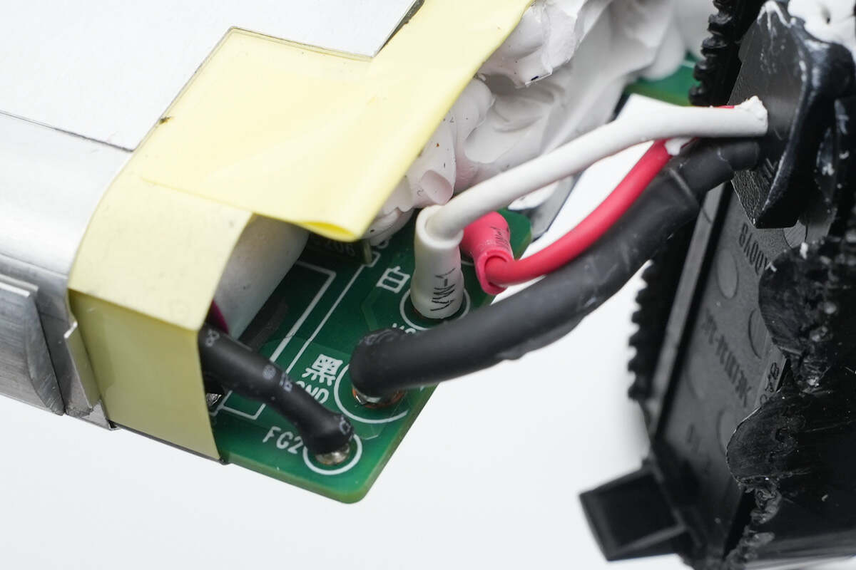
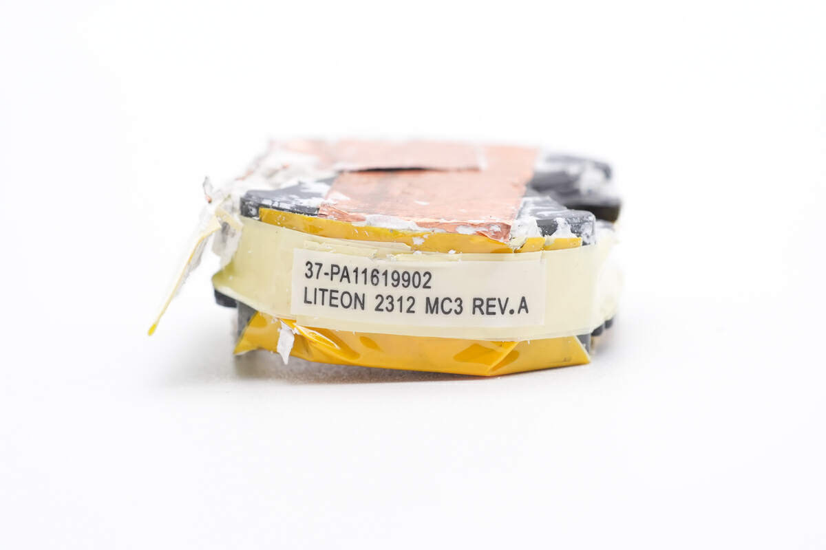
The filter capacitor PCB and transformer are on the output end.
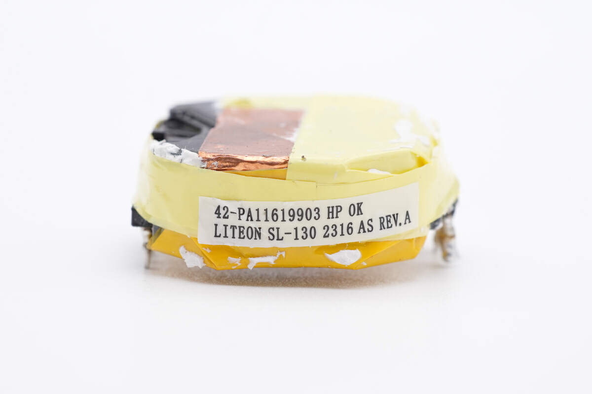
The transformer is wrapped in copper foil.
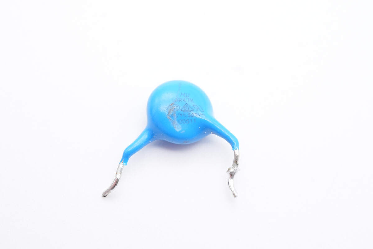
Here is the blue Y capacitor.
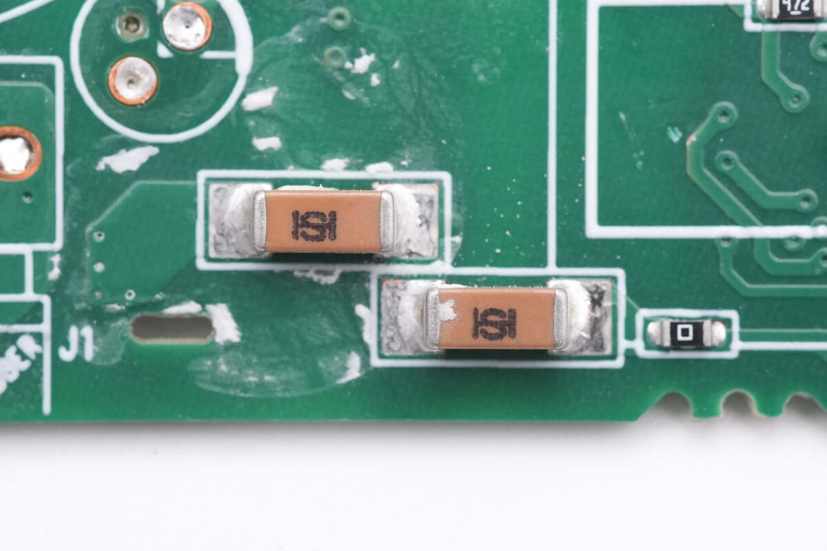
Two SMD Y capacitors are from Holy Stone and are connected in series.
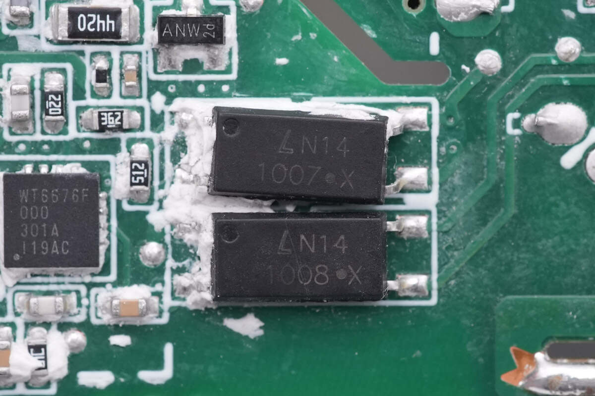
The LTV1007 and LTV1008 optocouplers are used to output voltage feedback and PFC control.
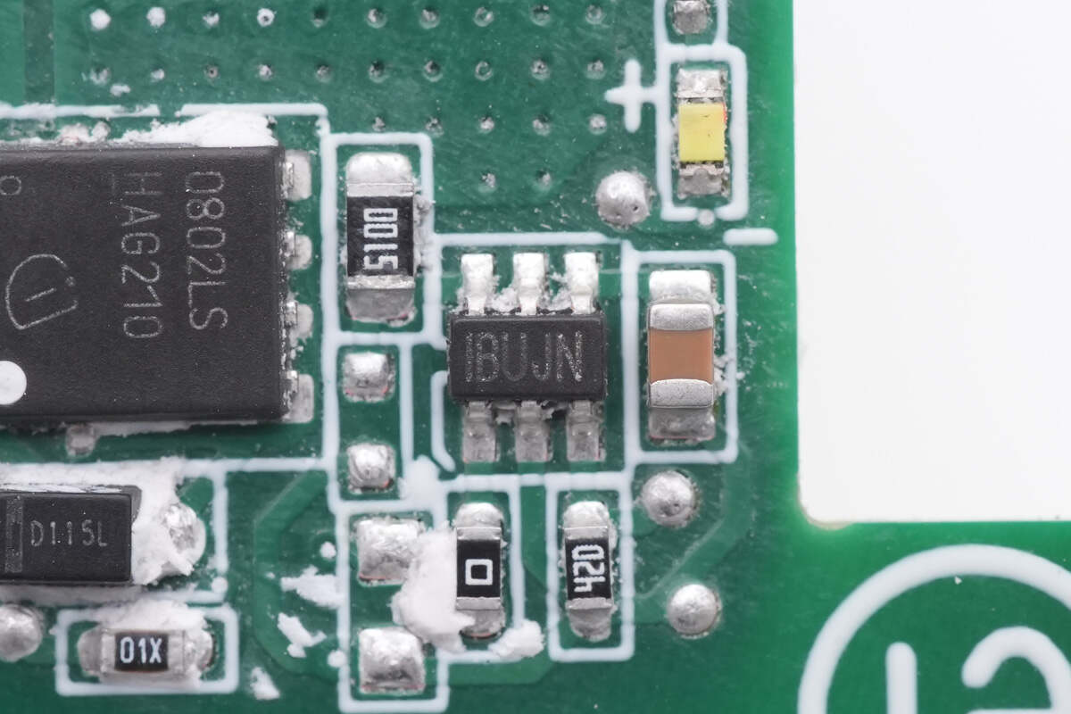
The synchronous rectifier controller marked with IBUJN is from MPS. It supports DCM, CCM, QR, ZVS, ACF (active clamp flyback), and HFB (hybrid-flyback). And its operating frequency can reach 1MHz, supports synchronous rectifier GaN FET, and adopts TSOT23-6 package. Model is MP6951.
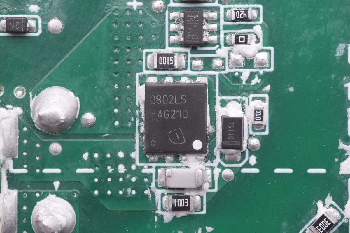
The synchronous rectifier MOSFET marked with 0802LS is from Infineon, and it adopts PG-TDSON-8 package. Model is BSC0802LS. 100V 3.4mΩ.
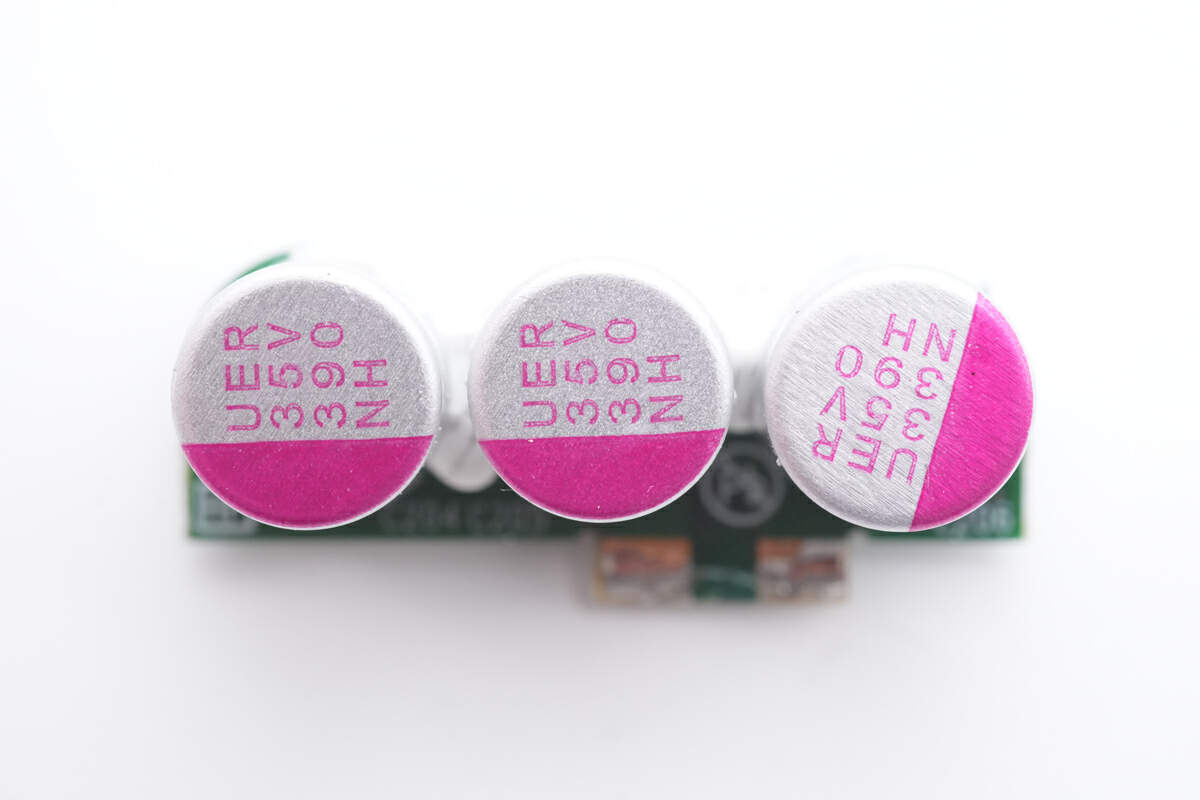
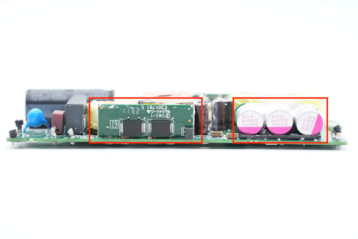
The solid capacitors for output filtering are from SAMXON UER series. It has 5000 hours of life. 35V 390μF.
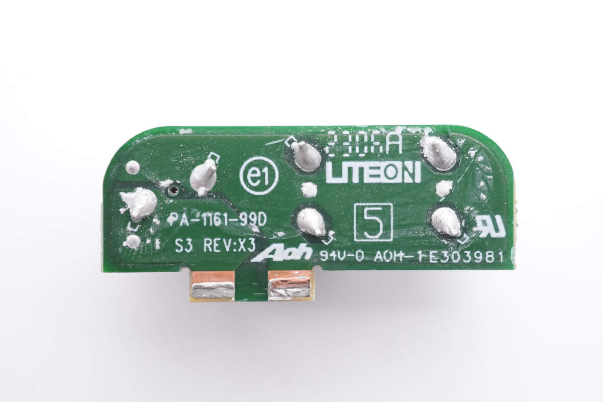
The filter capacitor PCB is marked with LITEON.
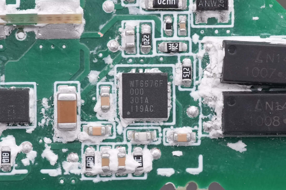
The USB PD protocol chip is from Weltrend, it supports USB PD3.1, 36V output, and programmable constant voltage and current control. It integrates a low-side current sampling amplifier and supports line loss compensation. Model is WT6676F.
It adopts a 10-bit ADC that can be used for voltage and current measurement. It supports an input power of 45V and adopts QFN-16 package. And the right side is a thermistor used to detect temperature.
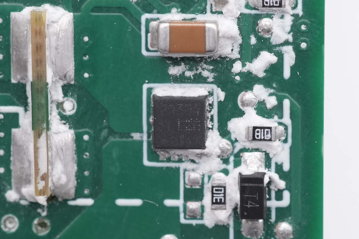
The output VBUS MOSFET is from Toshiba and adopts TSON Advance package. Model is TPN2R304PL. 40V 1.8mΩ.
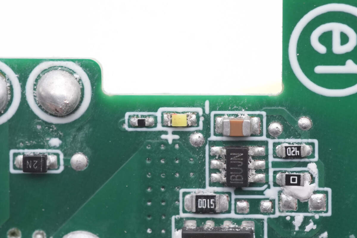
The SMD LED light is used for power indication.
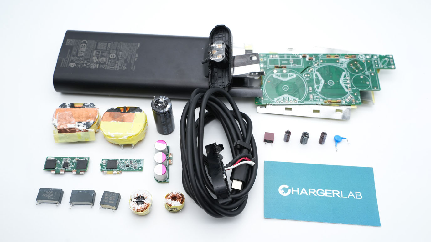
Well, those are all components of the power adapter.
Summary of ChargerLAB
The DELL 165W PD3.1 GaN Power Adapter can support 140W PD3.1 and 28V5.85A 165W.
It adopts the active bridge rectifier controller from NXP and the rectifier MOSFET from APEC. The PCBA module is filled with potting compound and pasted with aluminum sheets to enhance heat dissipation. And, the built quality is about the same as the 65W model.
There are many small PCBs vertically soldered on the PCBA, and an electrolytic capacitor is placed horizontally to improve space utilization.
Related Articles:
1. Teardown of Dell 60W USB-C GaN Power Adapter (HA60NM200)
2. Teardown of Dell 130W USB-C Power Adapter (HA130PM170)
3. Teardown of Dell 90W USB-C GaN Power Adapter Plus (PA901C)