Introduction
It's been a while since we took apart a power bank last time. Today, we got a powerful power bank from CUKTECH, called No.30. And we also made a introduction article for it, you can click here to have a look. It's equipped with a 40000 mAh battery pack and the total output power can be up to 300W. But you can still take it anywhere, like camping and traveling.
Product Appearance
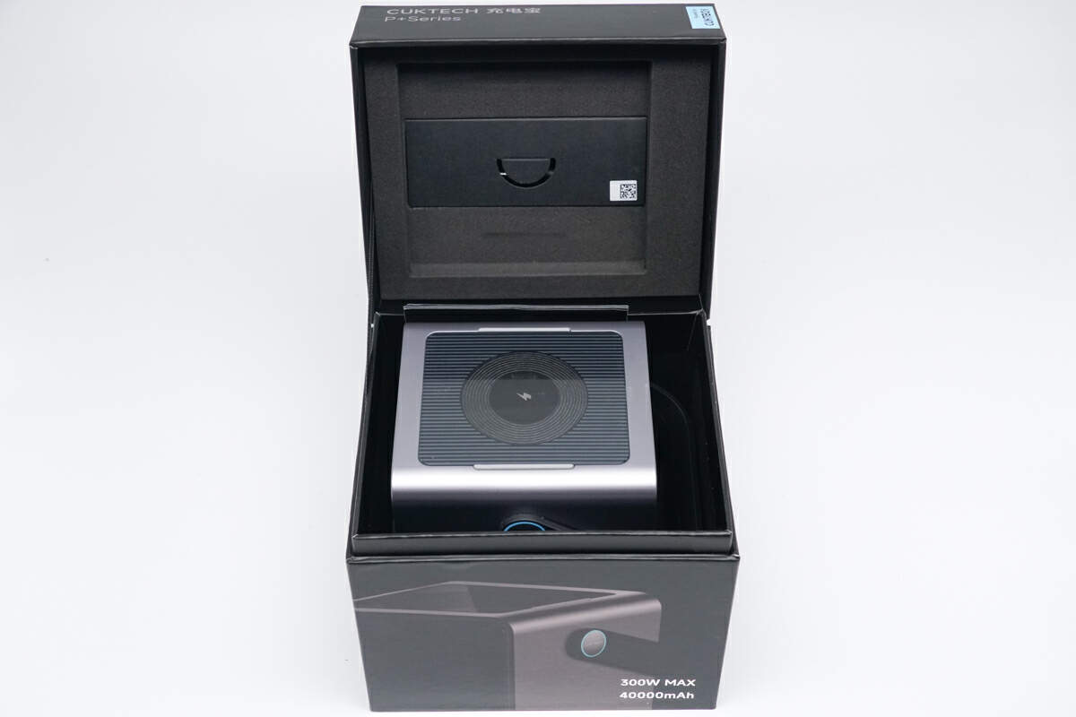
Let's open it first.
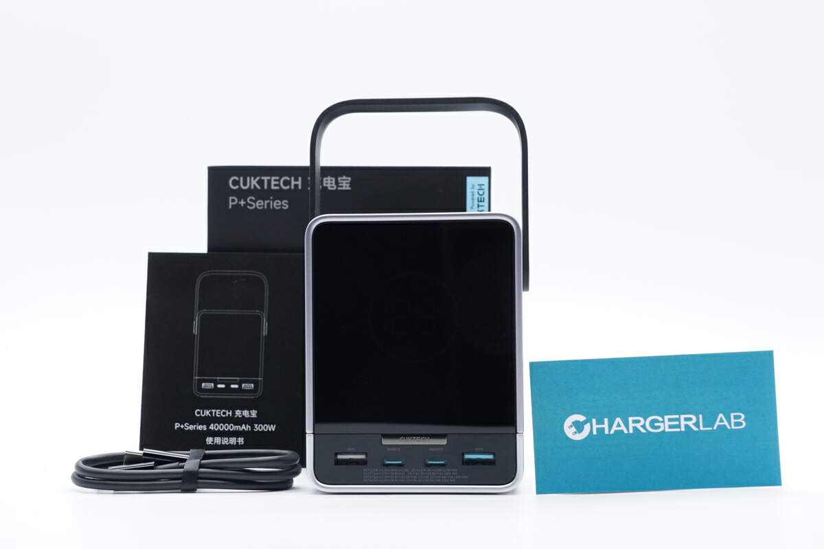
Except for the power bank itself, this box also contains the user manual and a cable.
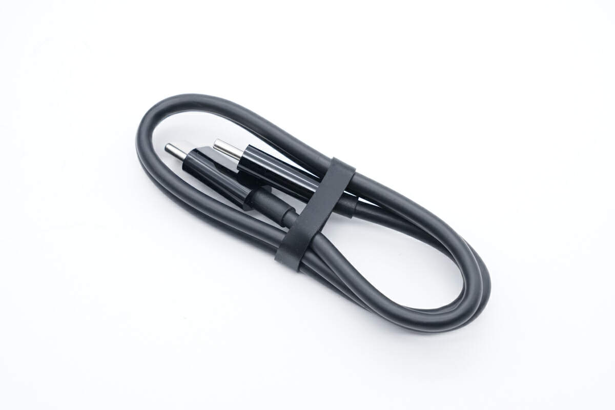
It's a short dual USB-C cable.
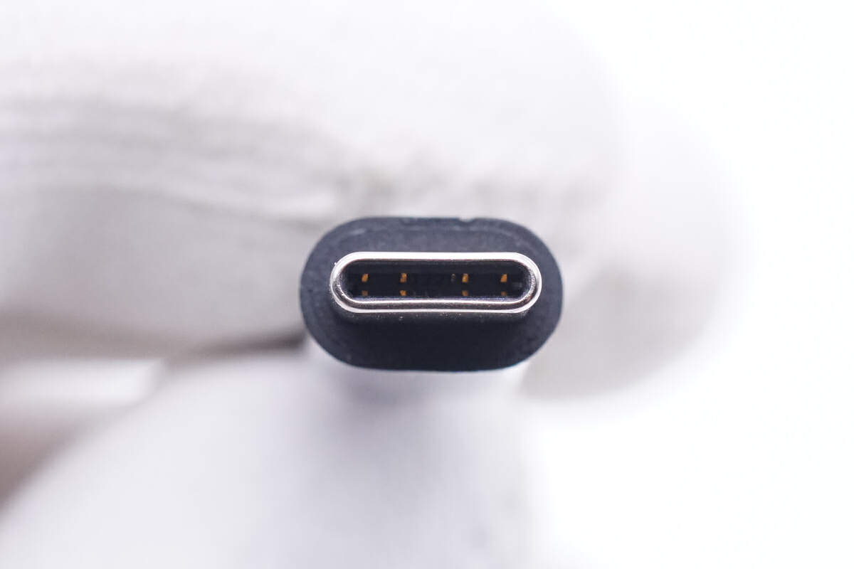
And it's not a "full-pin" design.
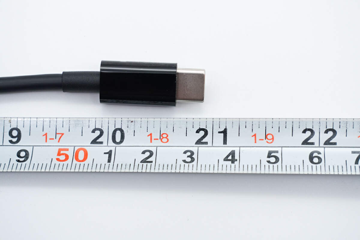
The length is about 53cm (1.74 ft).
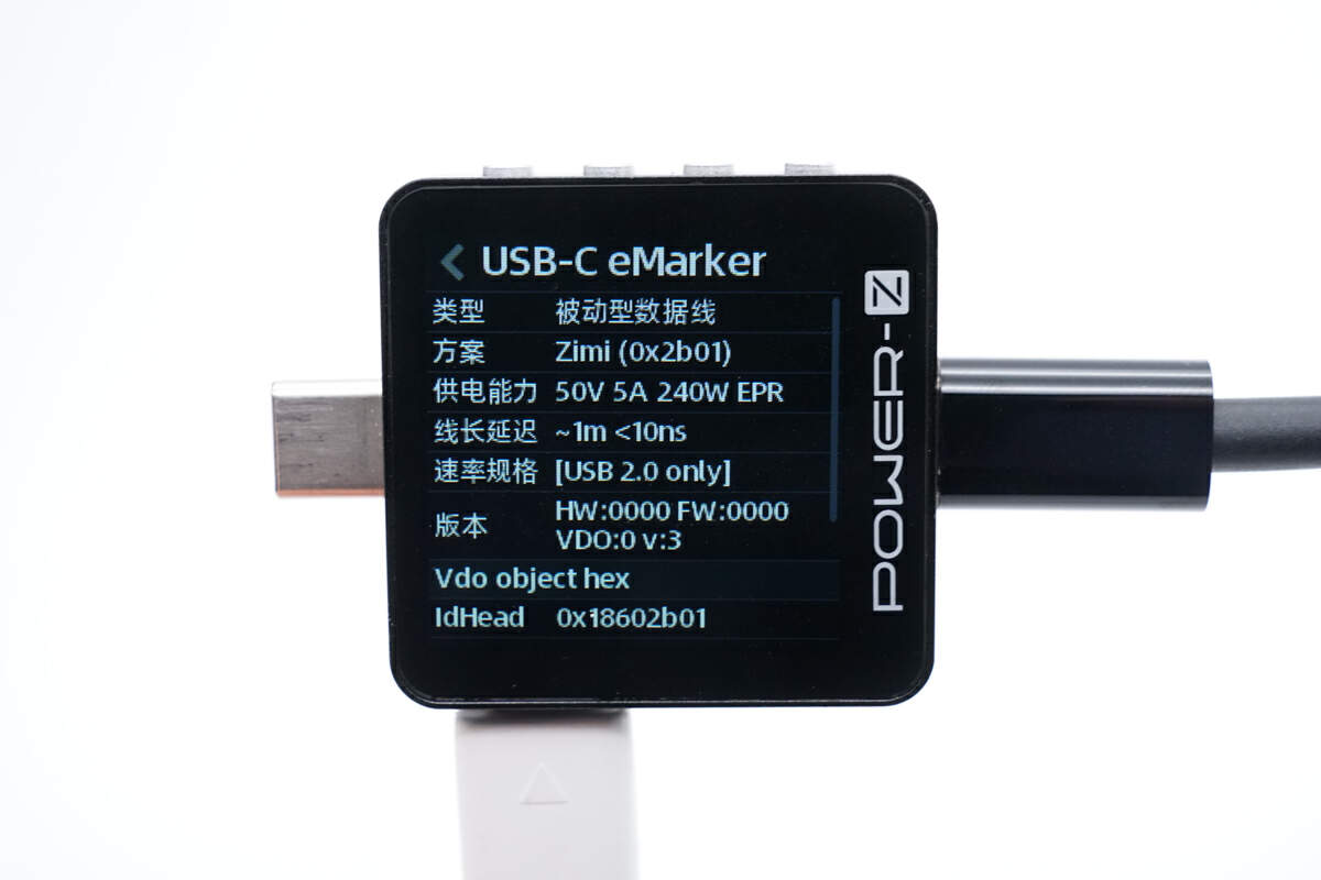
The ChargerLAB POWER-Z KM003C shows this USB-C cable has an E-marker chip and can support up to 240W.
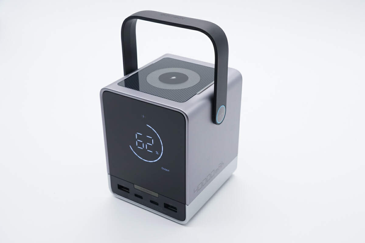
It has a display on the front, which shows the current status of this power bank.
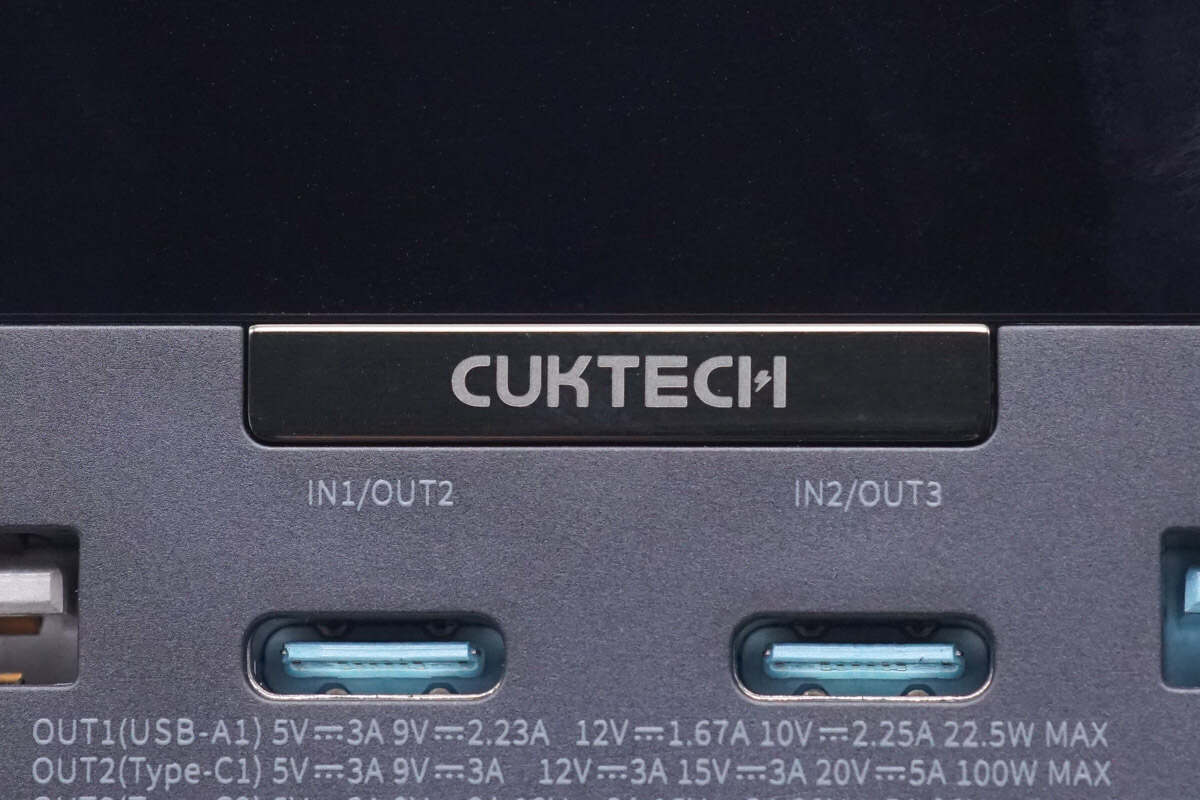
The power button is a strip, laser engraved CUKTECH.
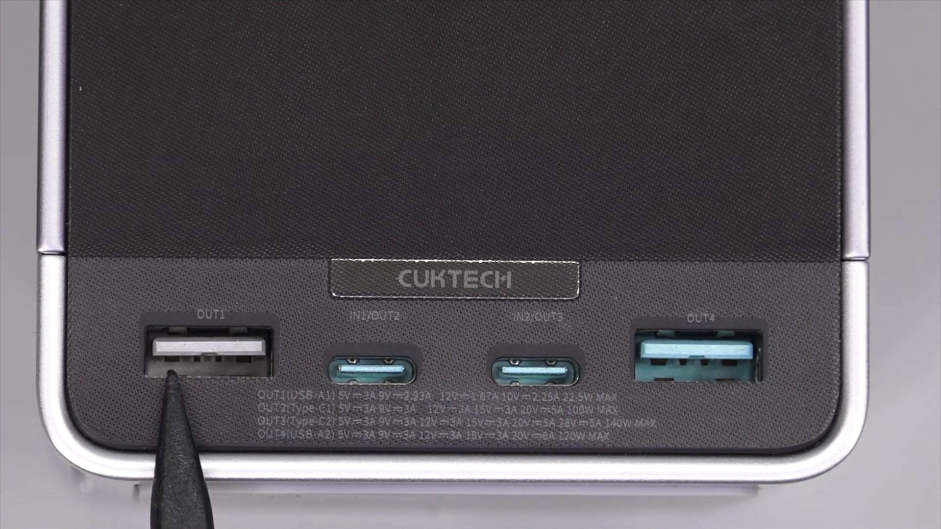
Two USB-C and two USB-A ports are at the bottom.
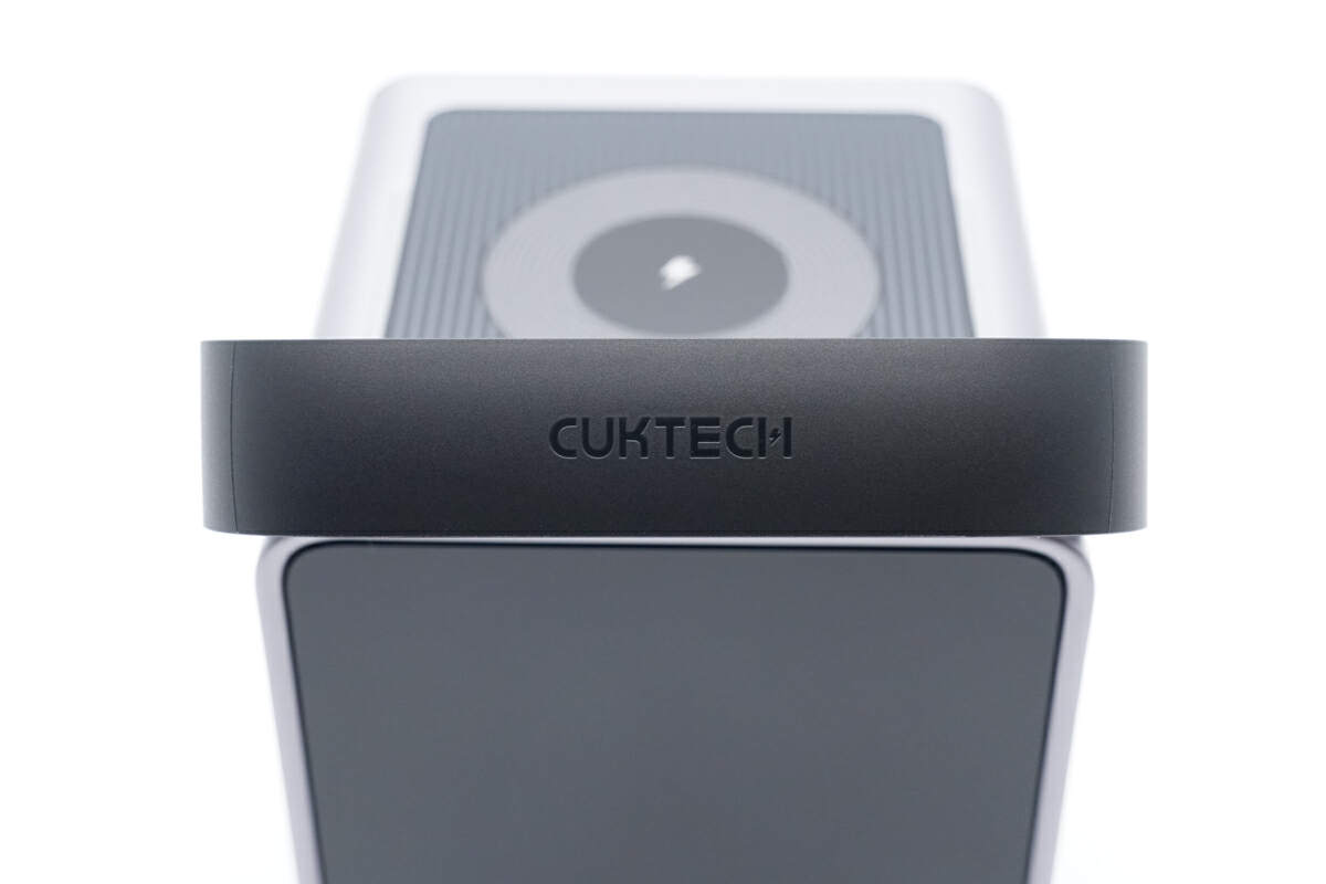
There is a plastic handle on the top for easy carrying, which also engraved with CUKTECH.
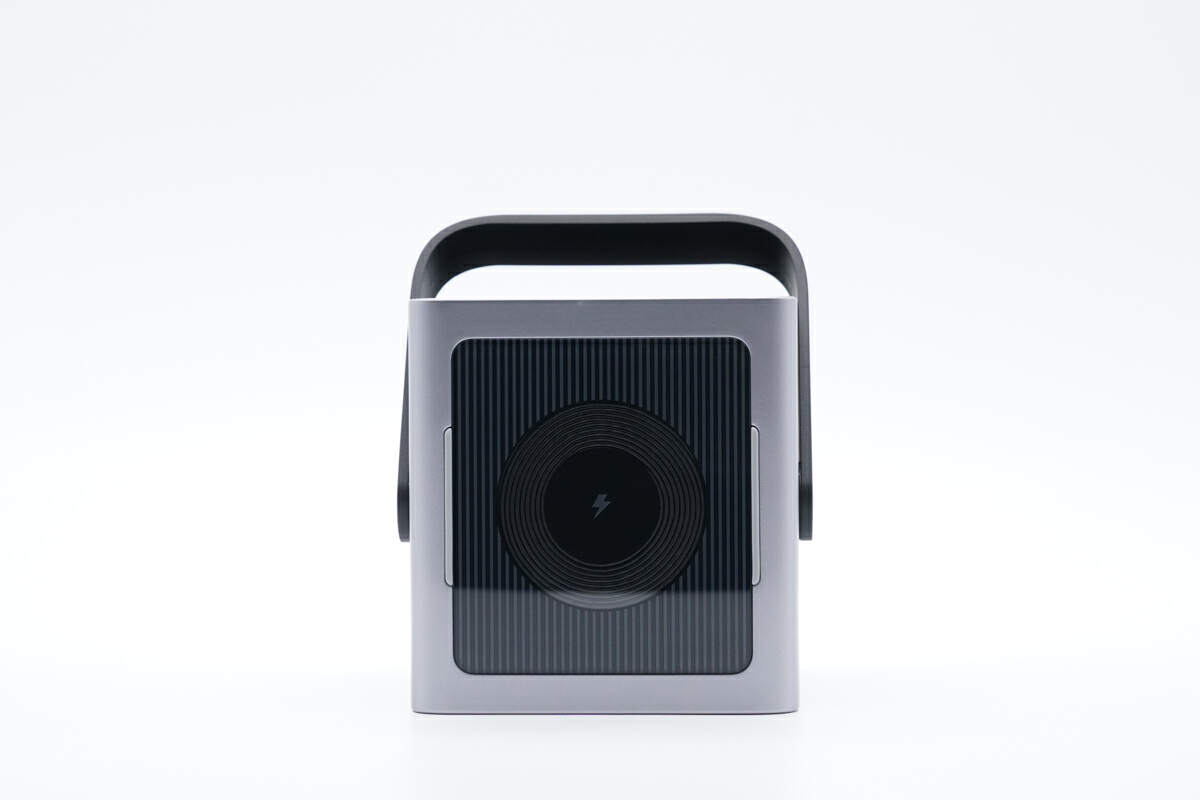
The wireless charging area is on the top, you can put your phone on it and start charging instantly.
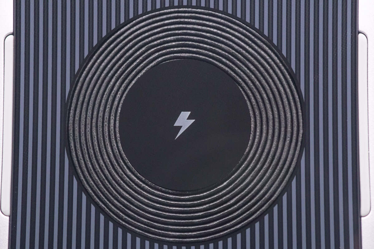
Take a closer look, you can actually see the charging coils inside due to its transparent design.
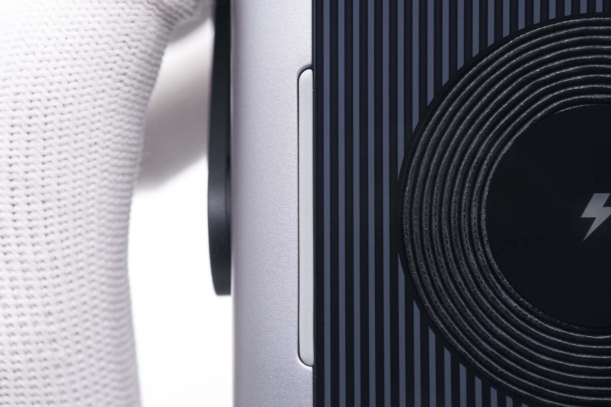
Two rubber strips on both sides are made for overheating issue of wireless charging.

Except for that, it also integrates a cooling fan on the back to improve heat dissipation performance.
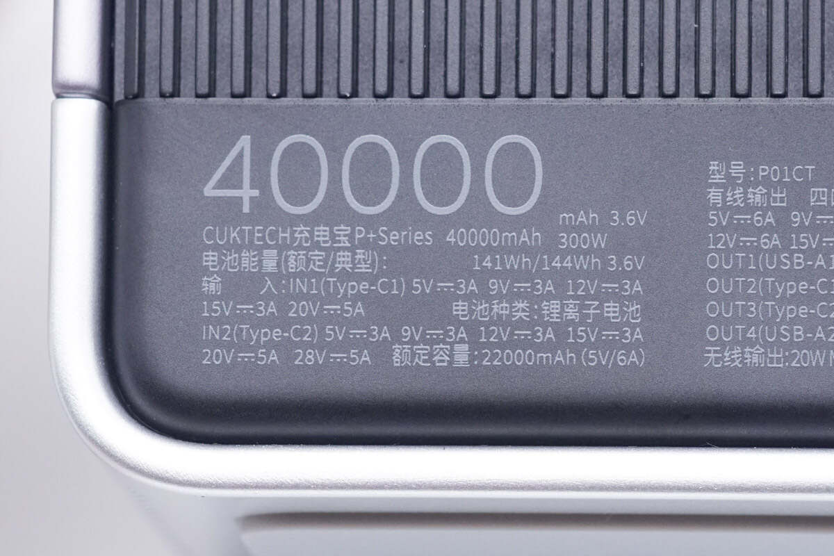
All specs info are below the cooling fan. Model is P01CT. The rated capacity is 141Wh.
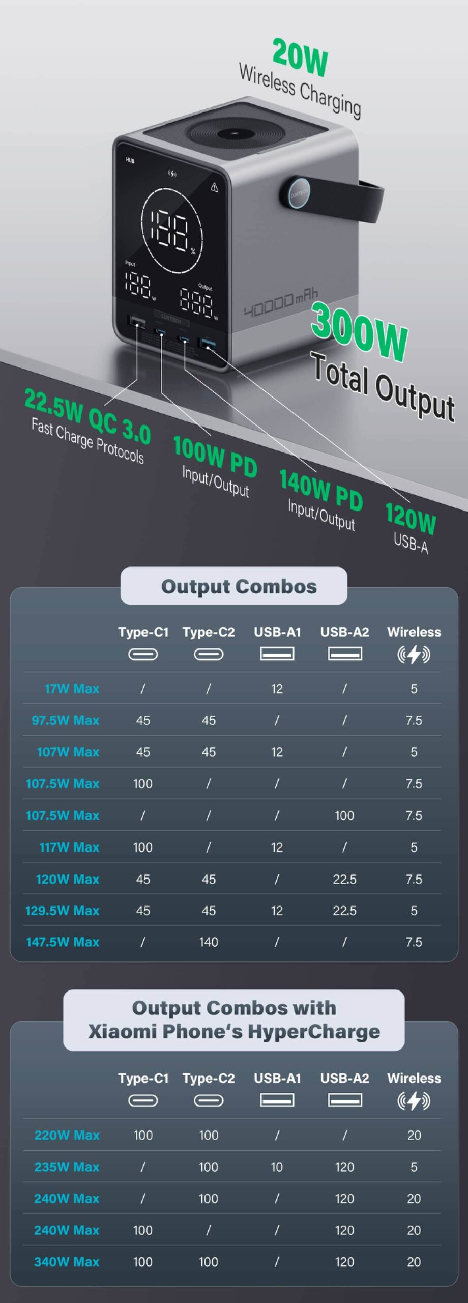
As for the output power of each port, you can check out this guide for details.
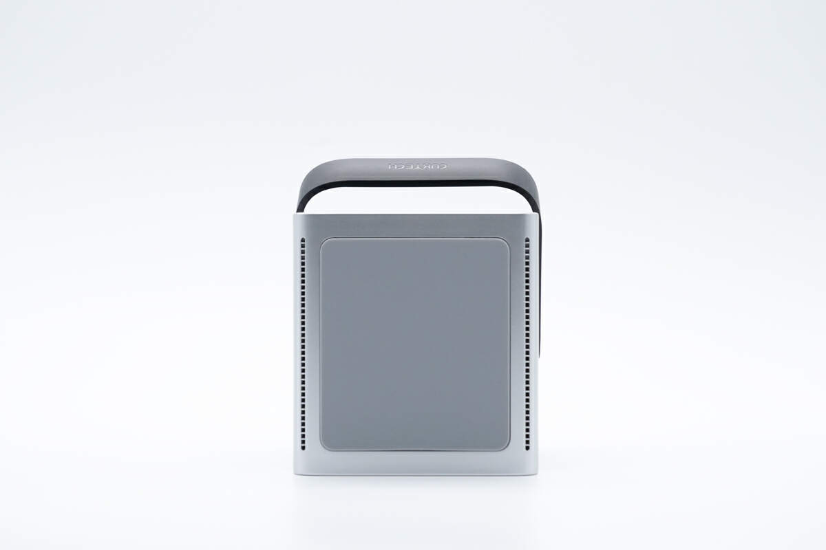
There is also a large silicone pad at the bottom of the power bank to ensure stability on the table.
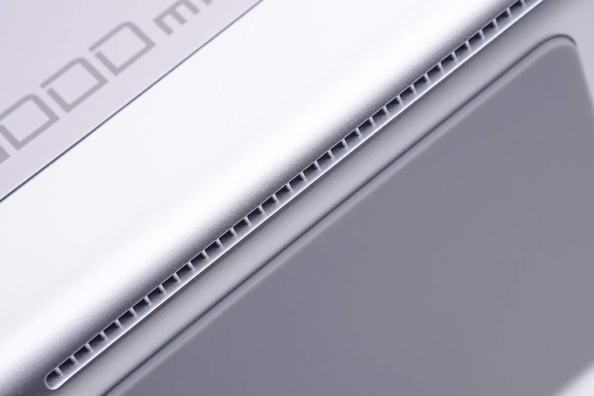
Furthermore, there are intake vents on both sides to complement the cooling fan, allowing for proper airflow and the establishment of an effective cooling system.
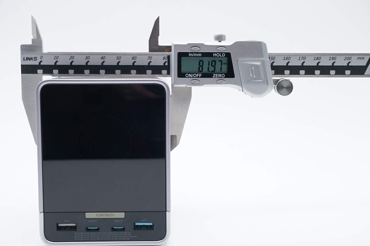
The length of this charger is about 82mm (3.23 inches).
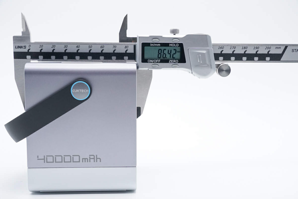
The width is about 86.5mm (3.41 inches).
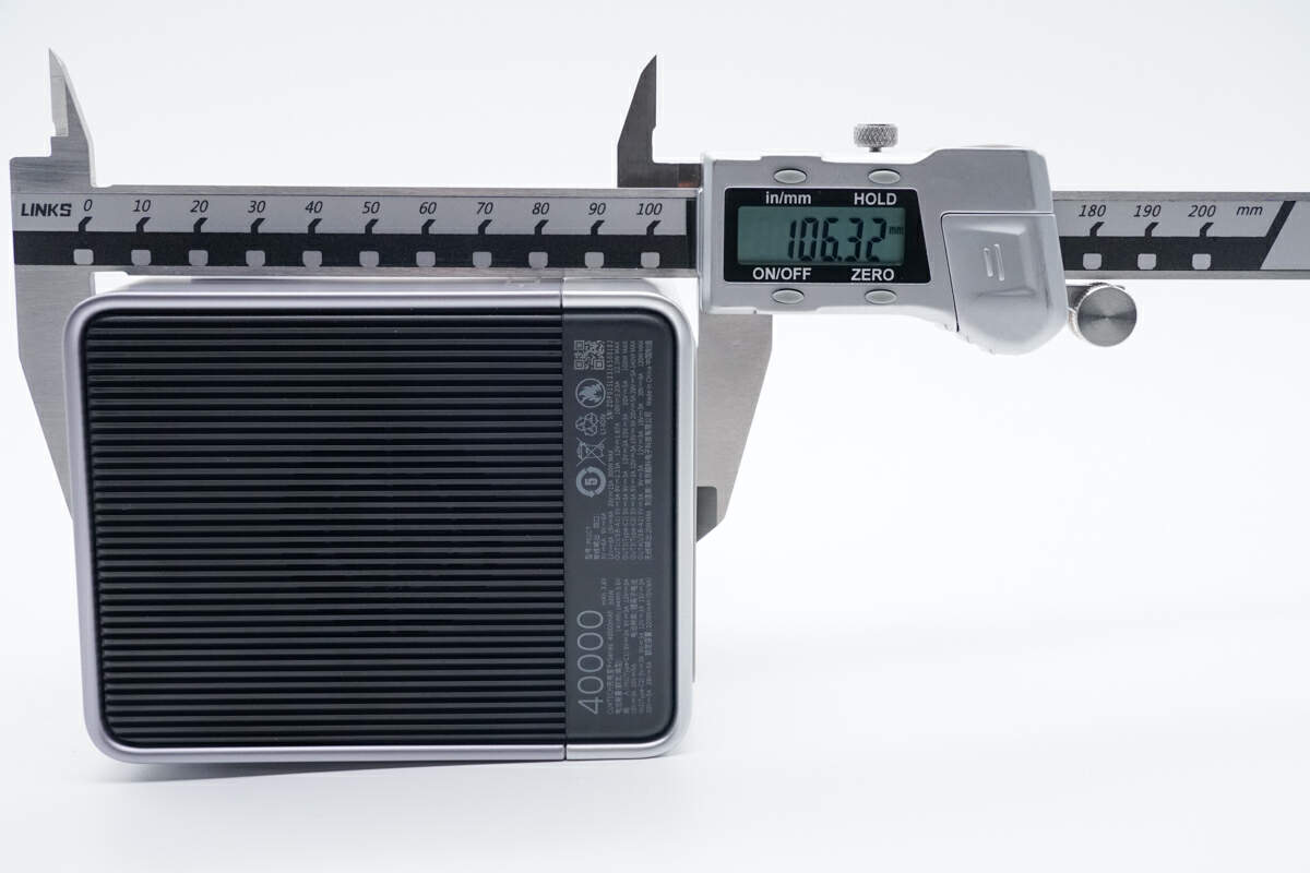
And the height is about 106mm (4.17 inches).
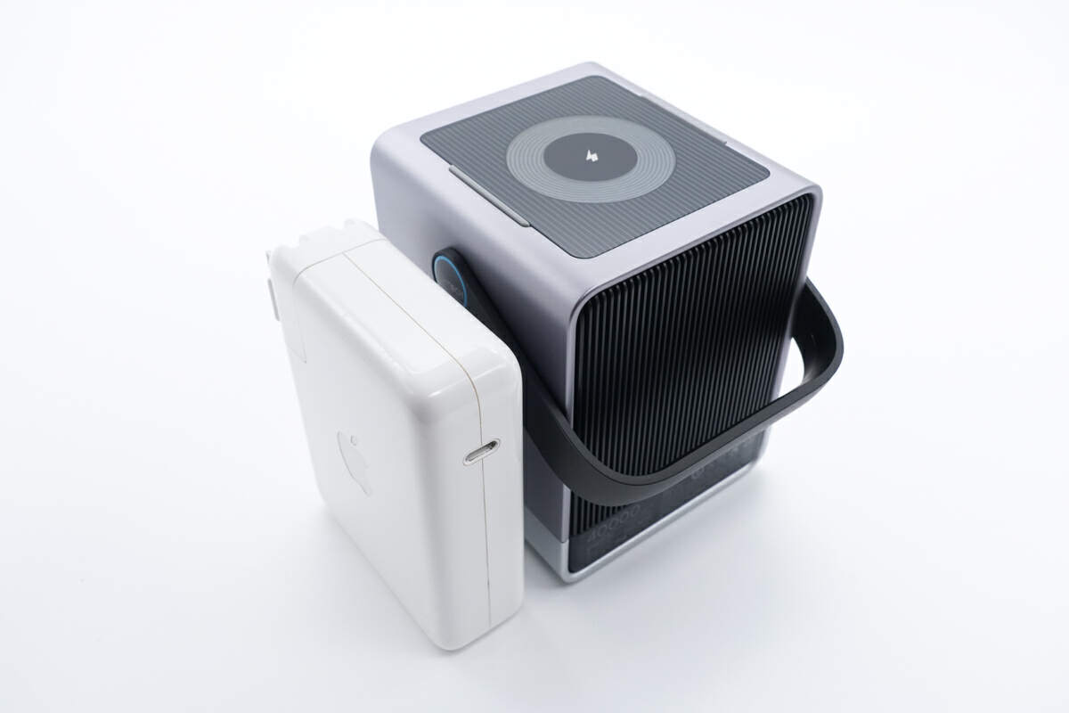
When compared side by side with the Apple 140W GaN charger, it may be slightly taller, but let's not forget that its maximum output power is twice that of Apple's.
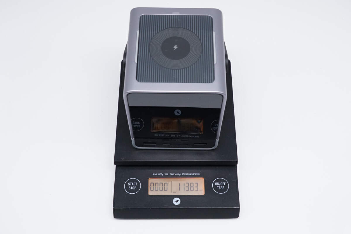
And the weight is about 1.13kg (2.49 lb).
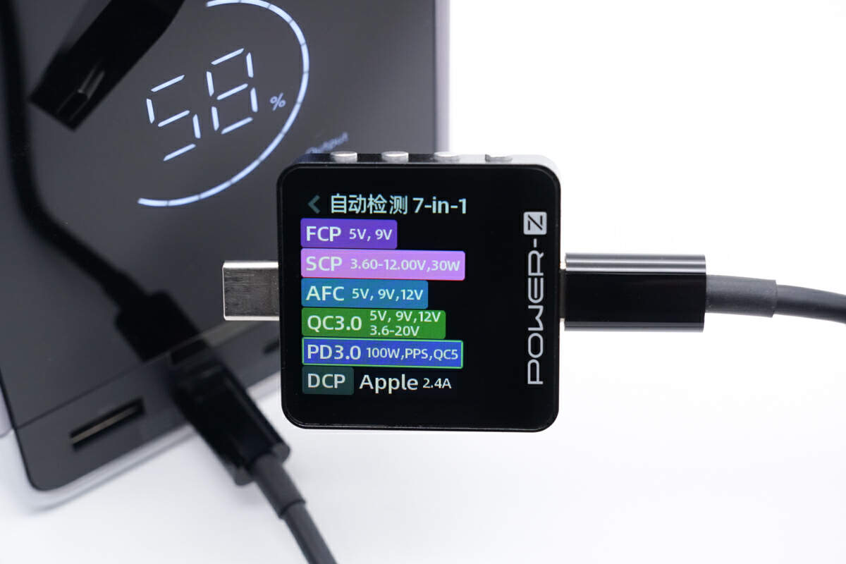
The ChargerLAB POWER-Z KM003C shows the USB-C1 supports FCP, SCP, AFC, QC3.0/5.0, PD3.0, PPS, DCP, and Apple 2.4A protocols.
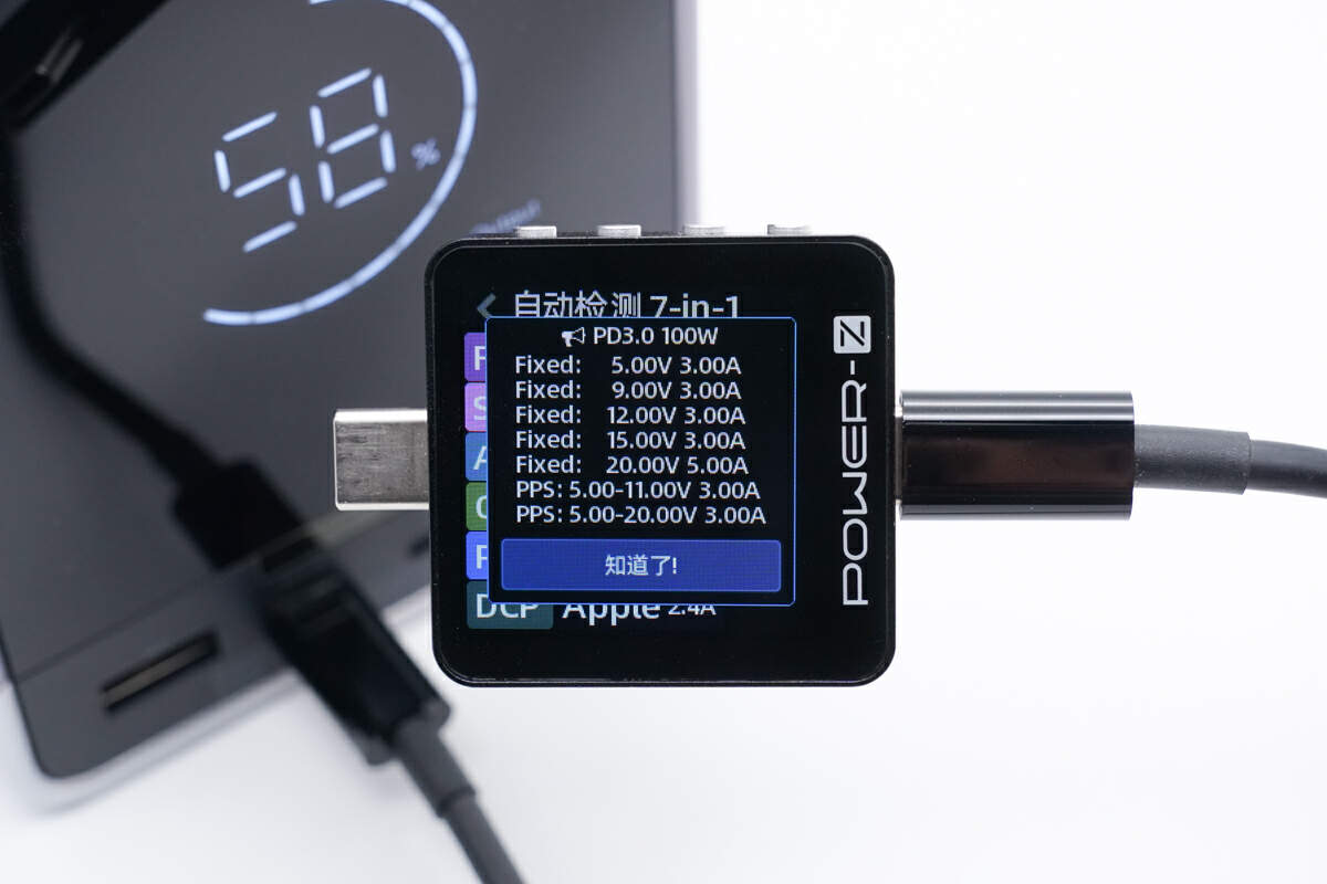
And the USB-C1 also supports five fixed PDOs of 5V/9V/12V/15V 3A, 20V 5A, and two sets of PPS.
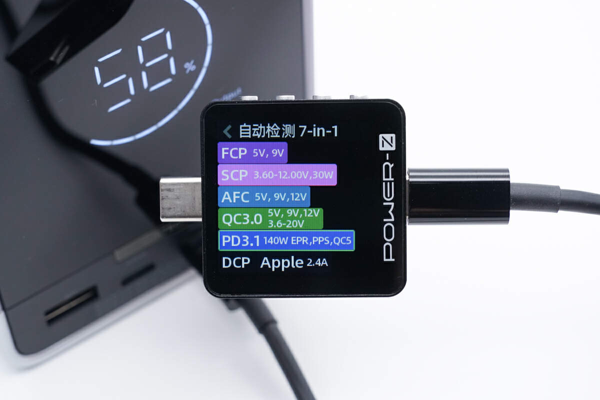
The biggest difference of USB-C2 is that it supports the USB PD3.1 protocol.
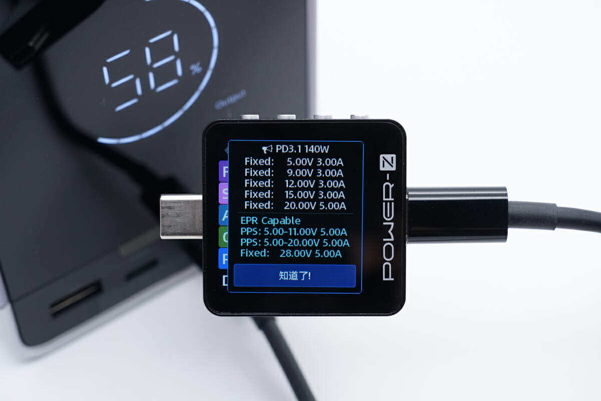
It has six fixed PDOs of 5V/9V/12V/15V 3A, 20V/28V 5A, and two sets of PPS.
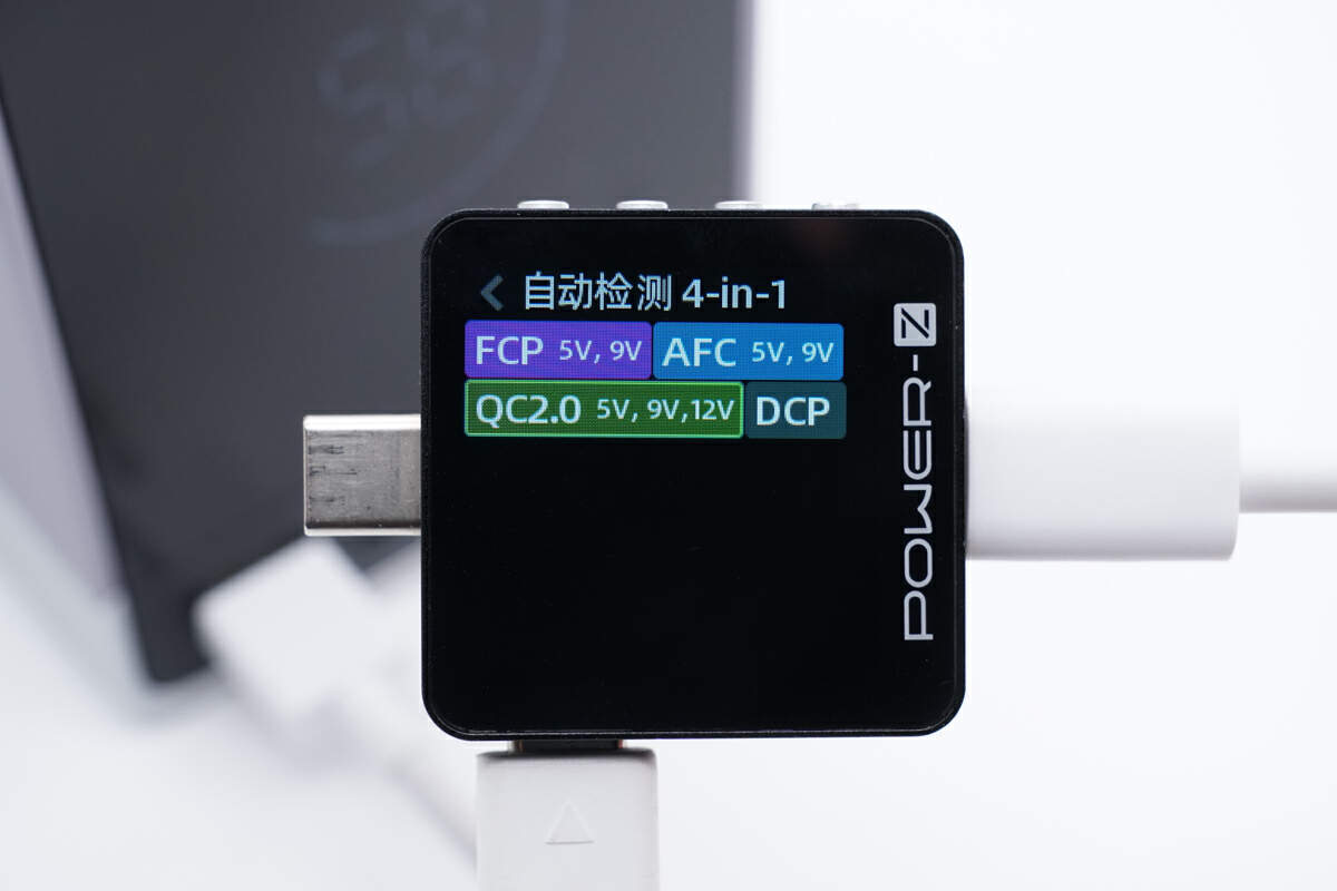
As for USB-A1, it supports FCP, AFC, QC2.0, DCP protocols.
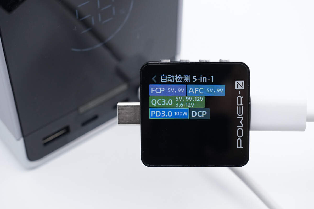
And USB-A2 supports FCP, AFC, QC3.0, PD3.0, and DCP protocols.
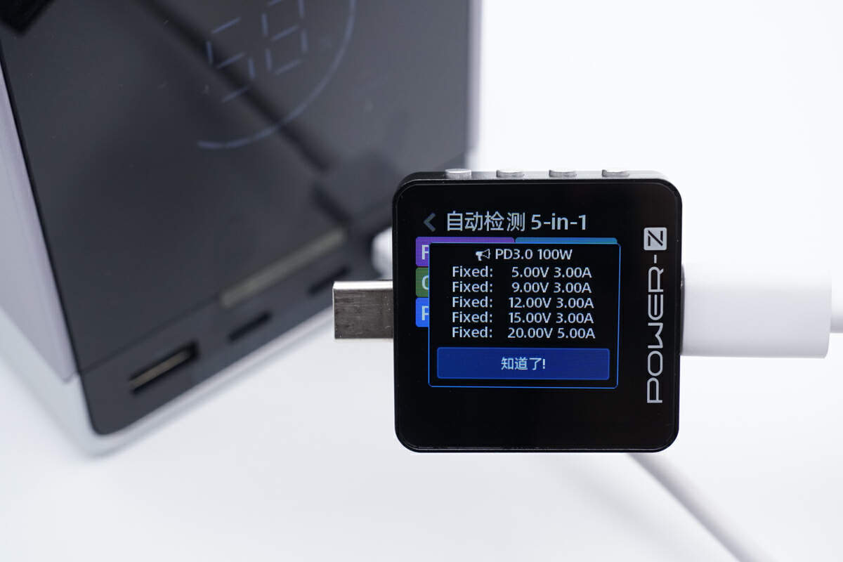
The USB-A2 also supports five fixed PDOs of 5V/9V/12V/15V 3A, 20V 5A.
Teardown
Next, let's try to take apart this power bank from the front panel.
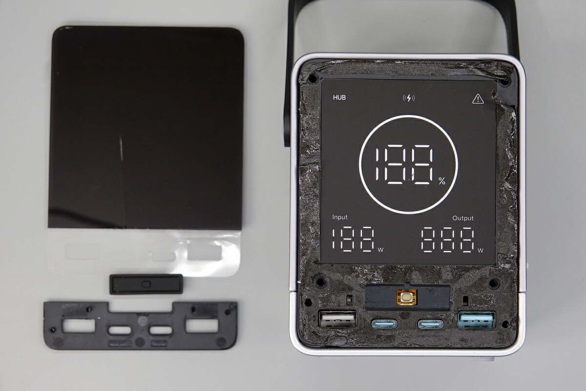
The display is fixed with double-sided tape and screws.
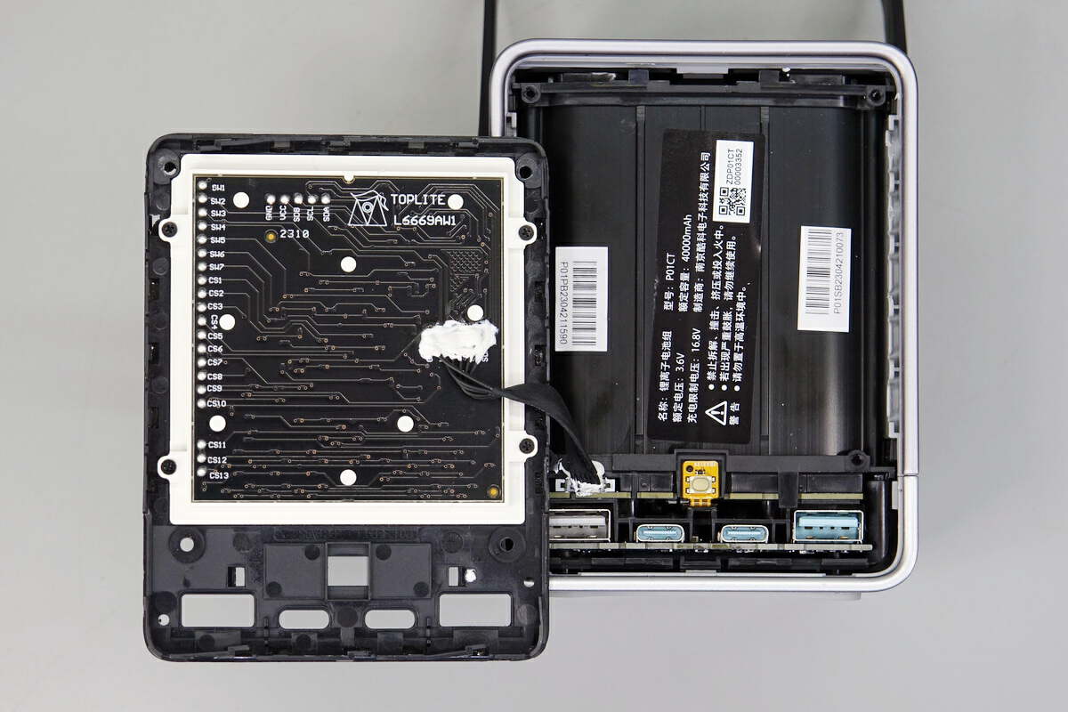
Remove those screws.
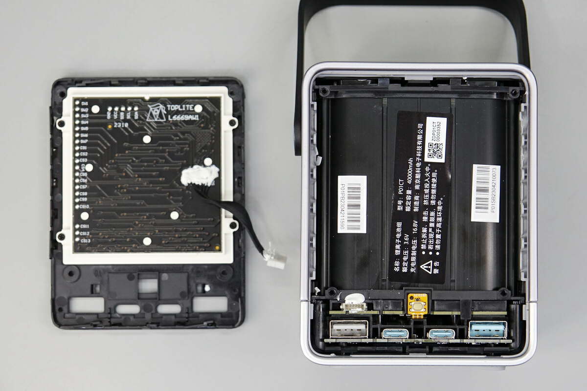
And disconnect the front panel from the battery.
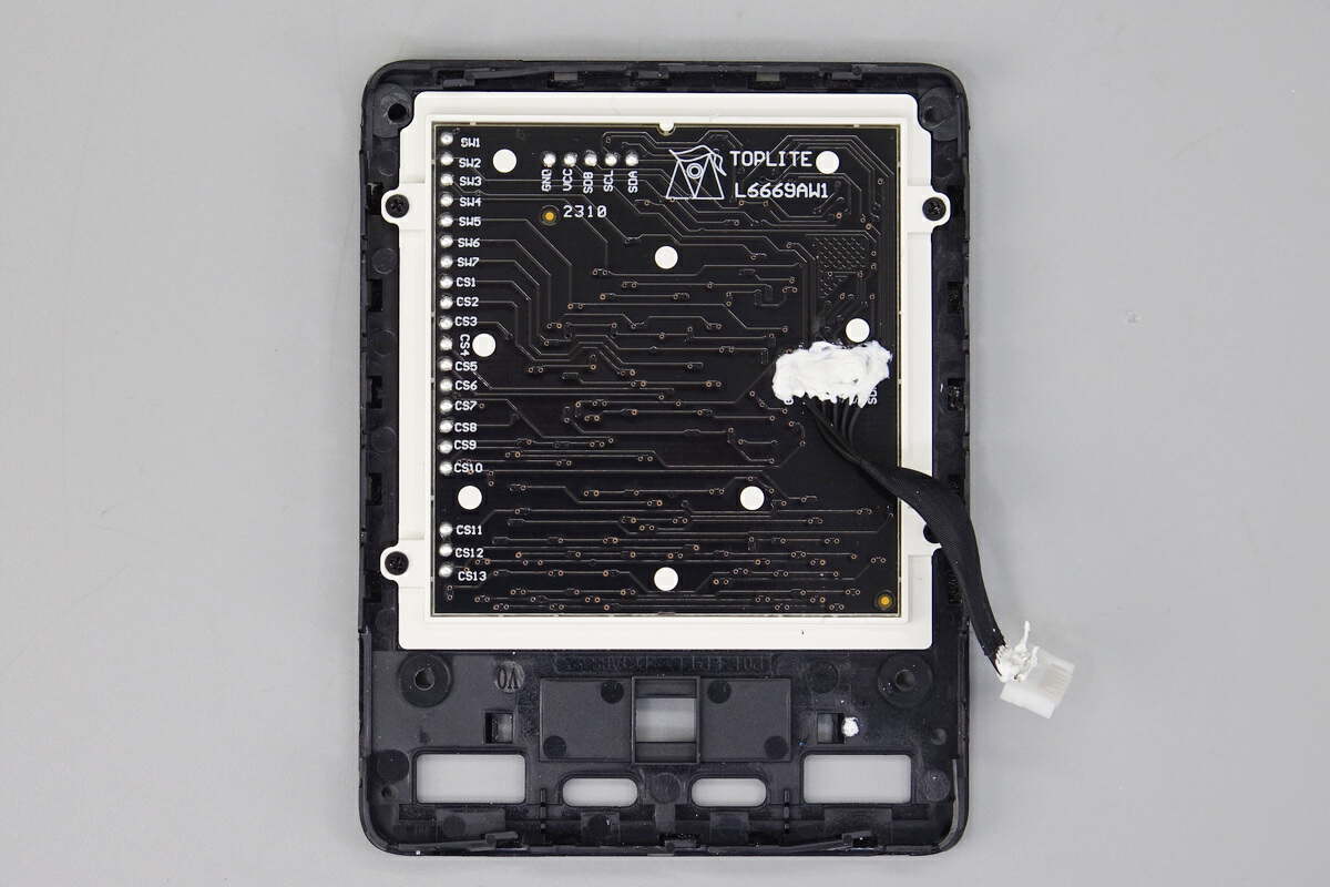
The solder joints are covered with silicone adhesives.
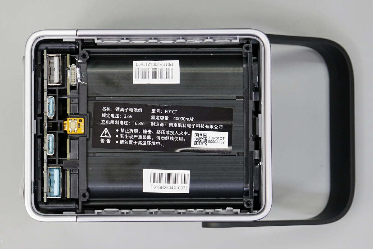
Most of the internal space is occupied by the battery pack. The model is P01CT, and the rated voltage is 3.6V.
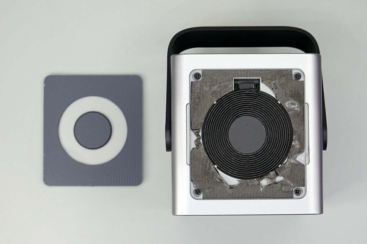
The top wireless charging area is also fixed with double-sided tape and screws.
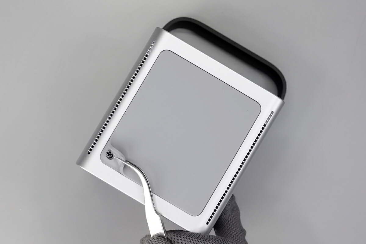
Tear off the silicone pad at the bottom.
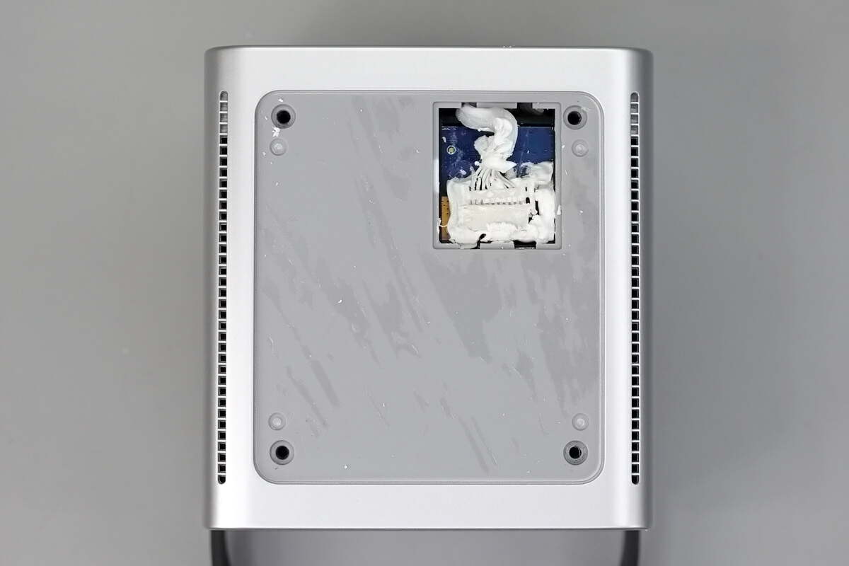
Here is the connector of wireless charging module.
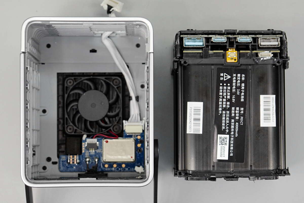
Then, take out the entire battery pack.
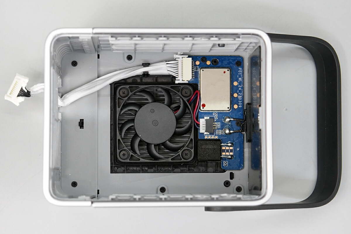
We can see the cooling fan inside.
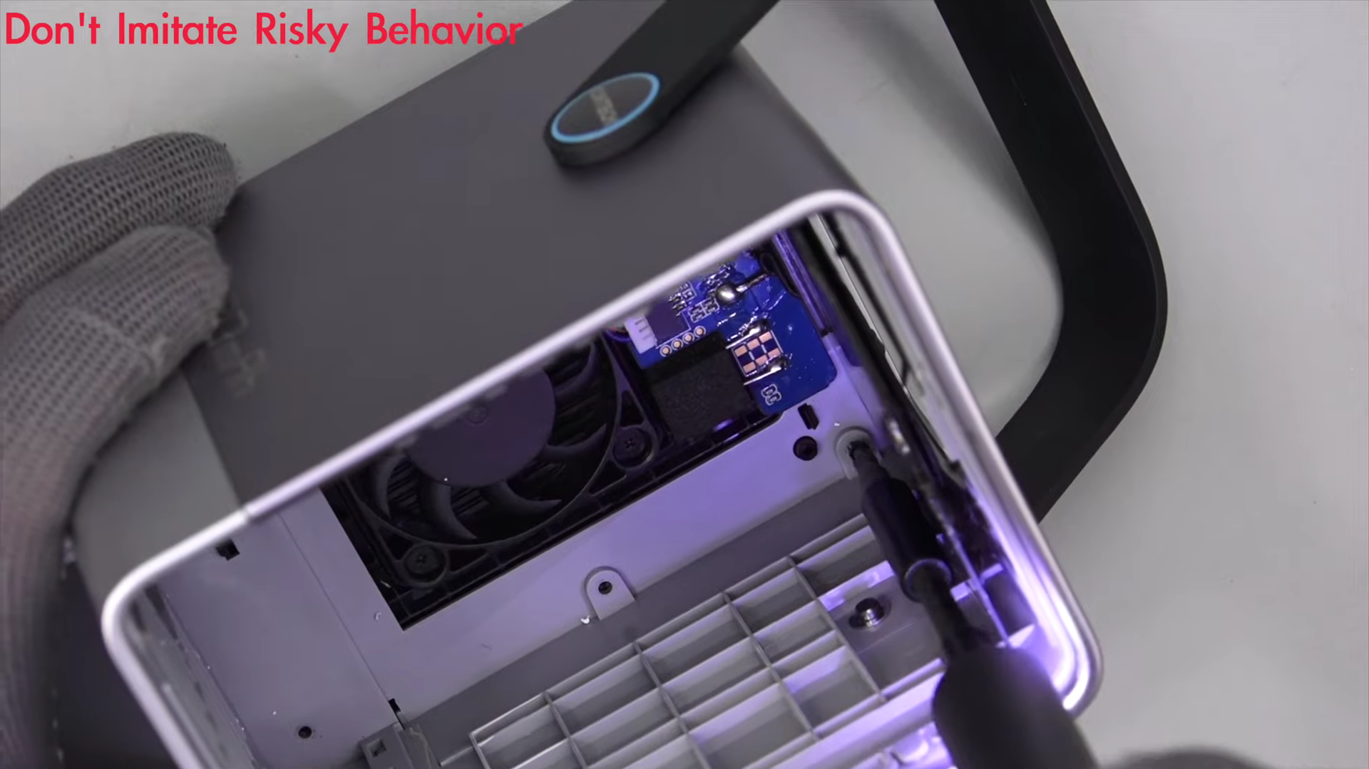
Continue to remove the remaining screws.
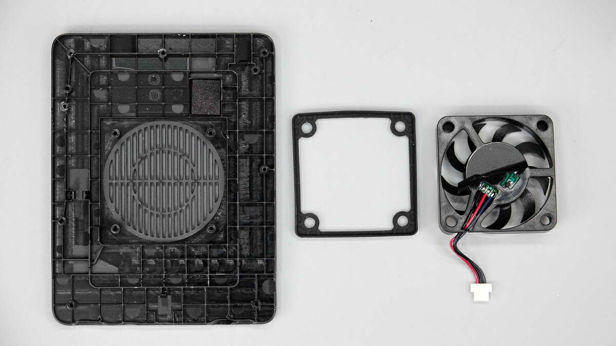
And separate the cooling fan.
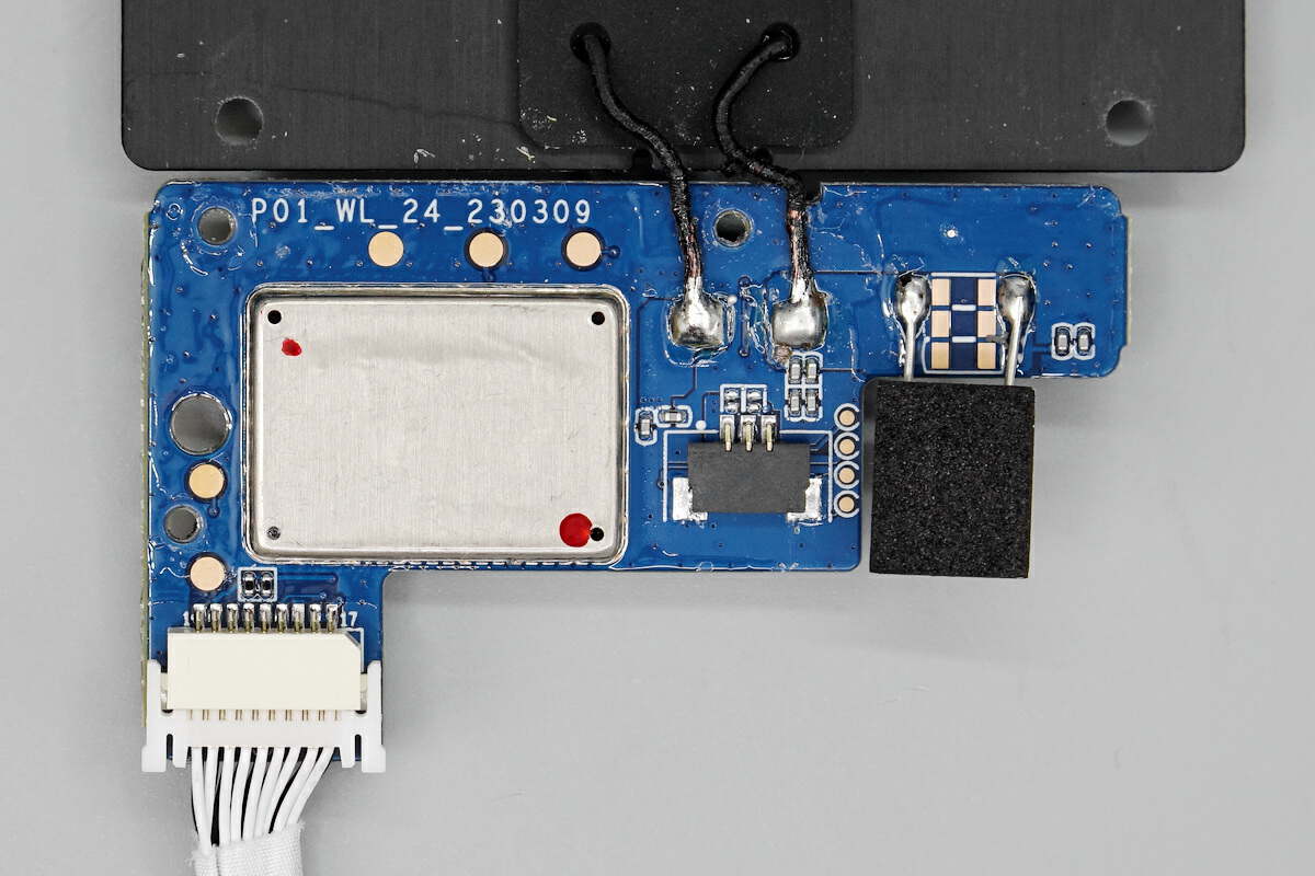
First, let's introduce the PCBA module for wireless charging.
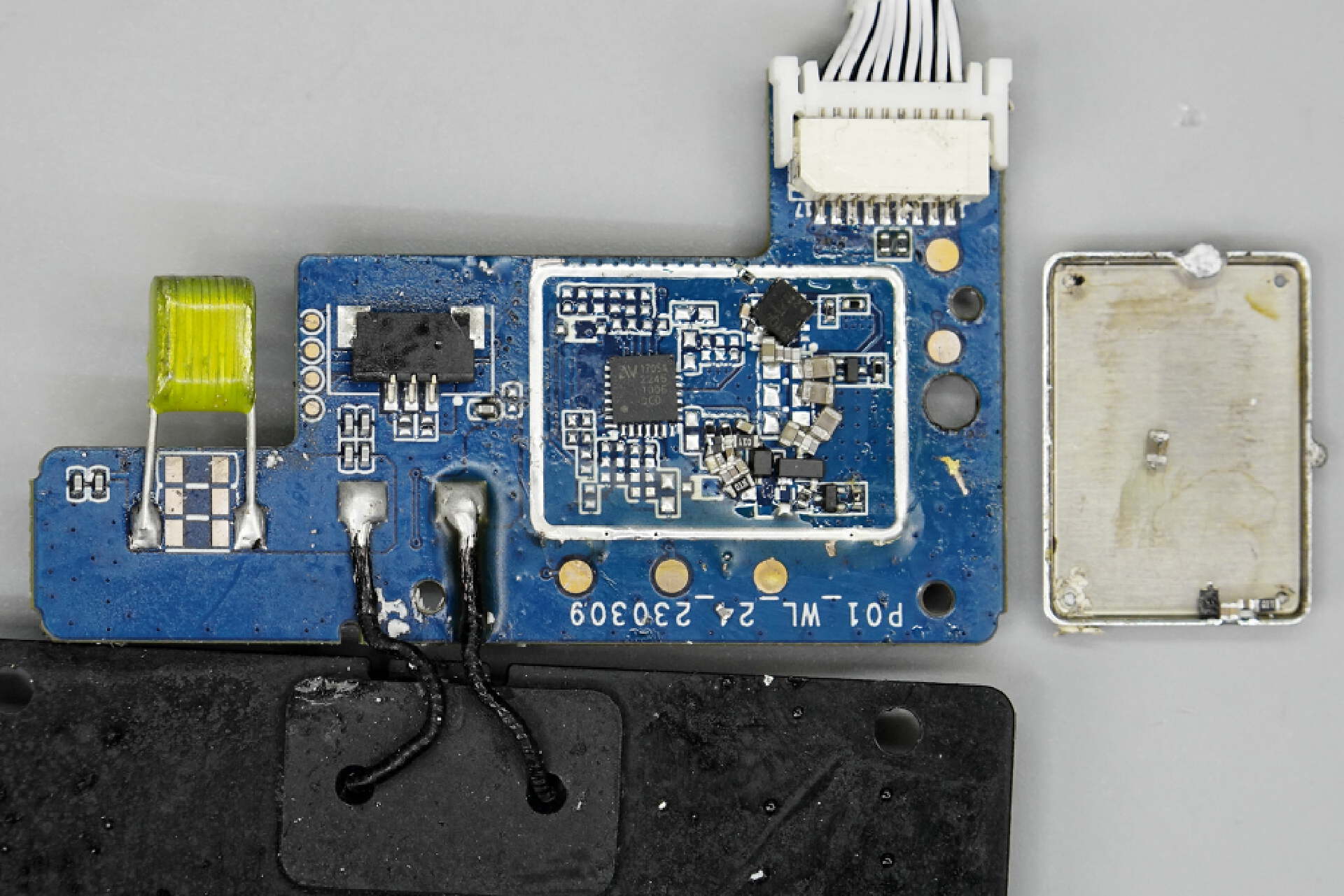
The charging circuit is under the metal shield.
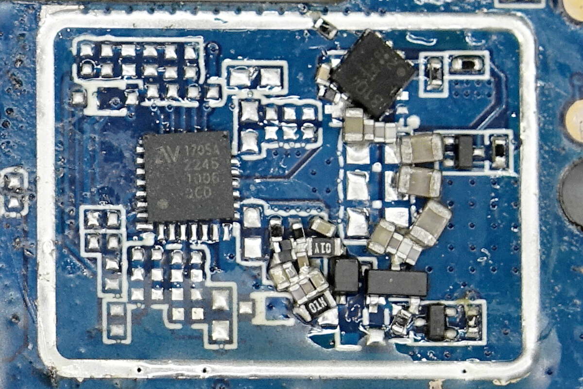
During the teardown of the metal shield, the components' positions were accidentally disturbed due to excessive temperature.
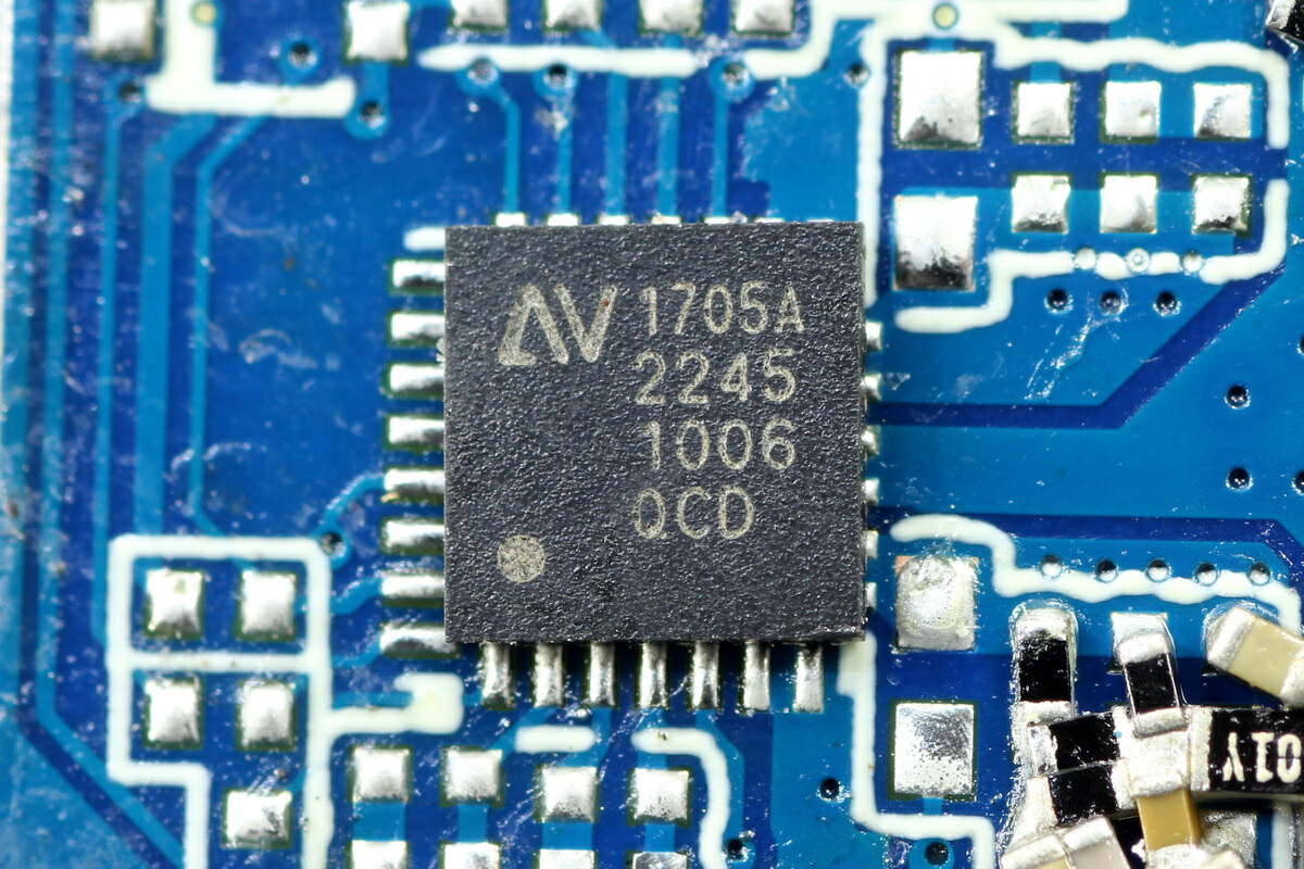
The wireless power transmitter is from NuVolta, model is NU1705. It integrates many critical functions, such as a full-bridge power stage, a 32bit MCU core, low-EMI drivers, bootstrap circuit, as well as multiple protection functions.
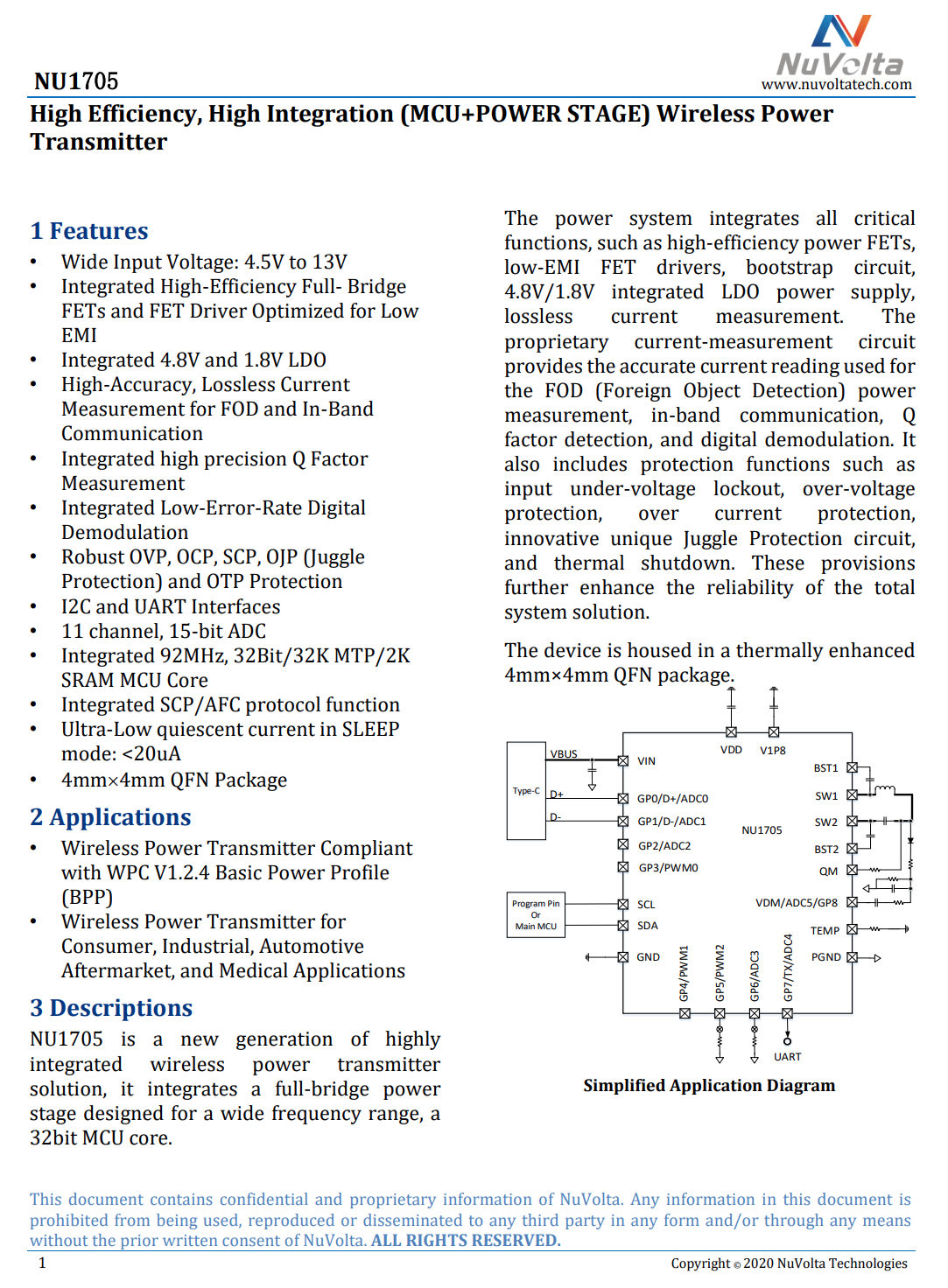
Here is all the information about NuVolta NU1705.
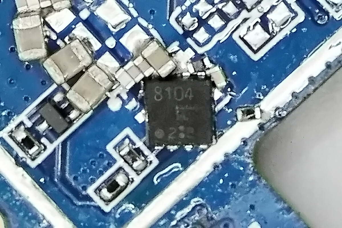
The MOSFET is from Toshiba. 30V 6.8mΩ. Model is TPCC8104.
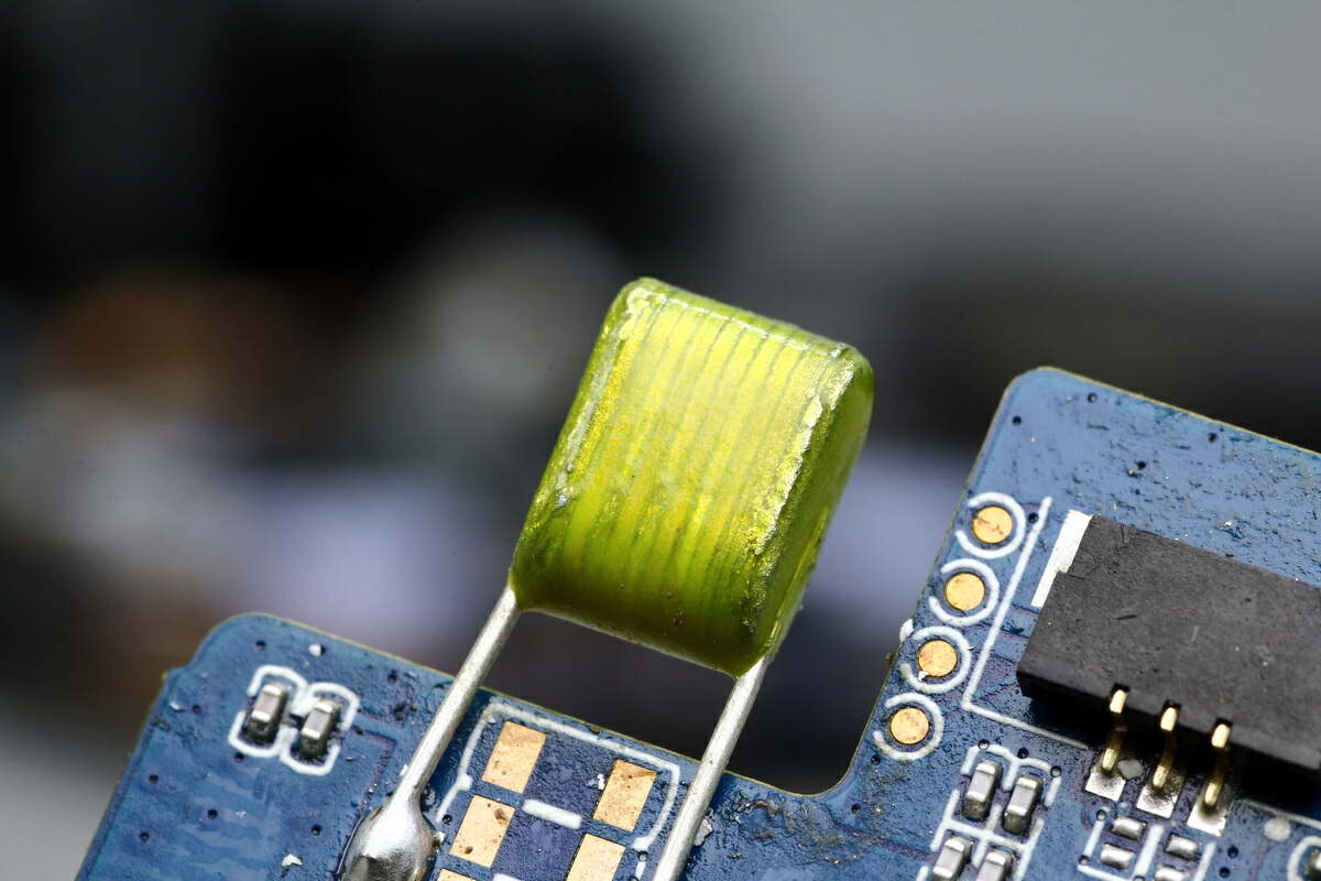
The resonant capacitor is coated with yellow resin.
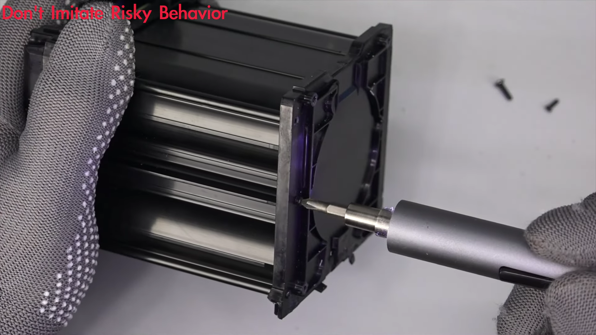
Next, let's remove all screws that fixed the battery pack.

And then, clean up the potting compound.
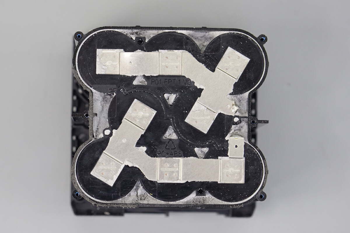
There're eight Samsung 21700 batteries inside, which are fixed by the plastic frame. Two sets of four batteries connected in series are connected in parallel.
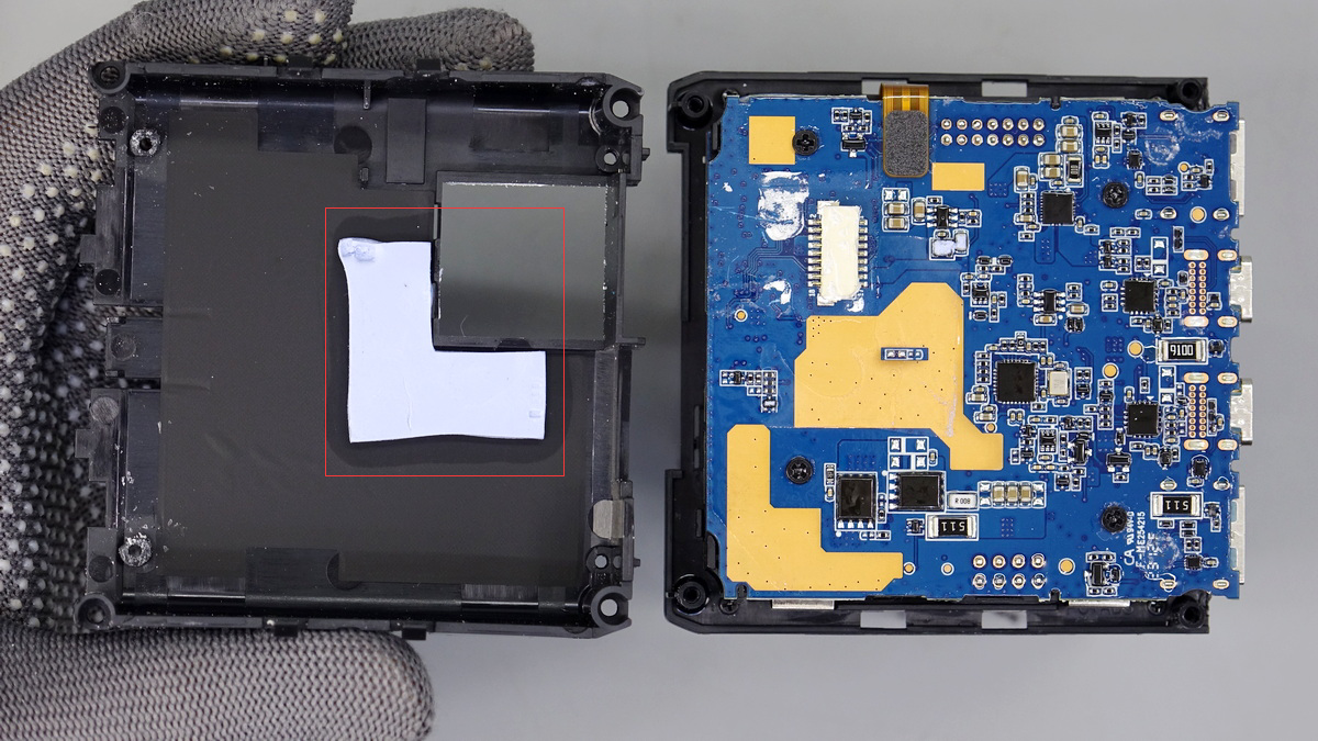
Then, let's check the other side. There's a thermal pad inside the cover.
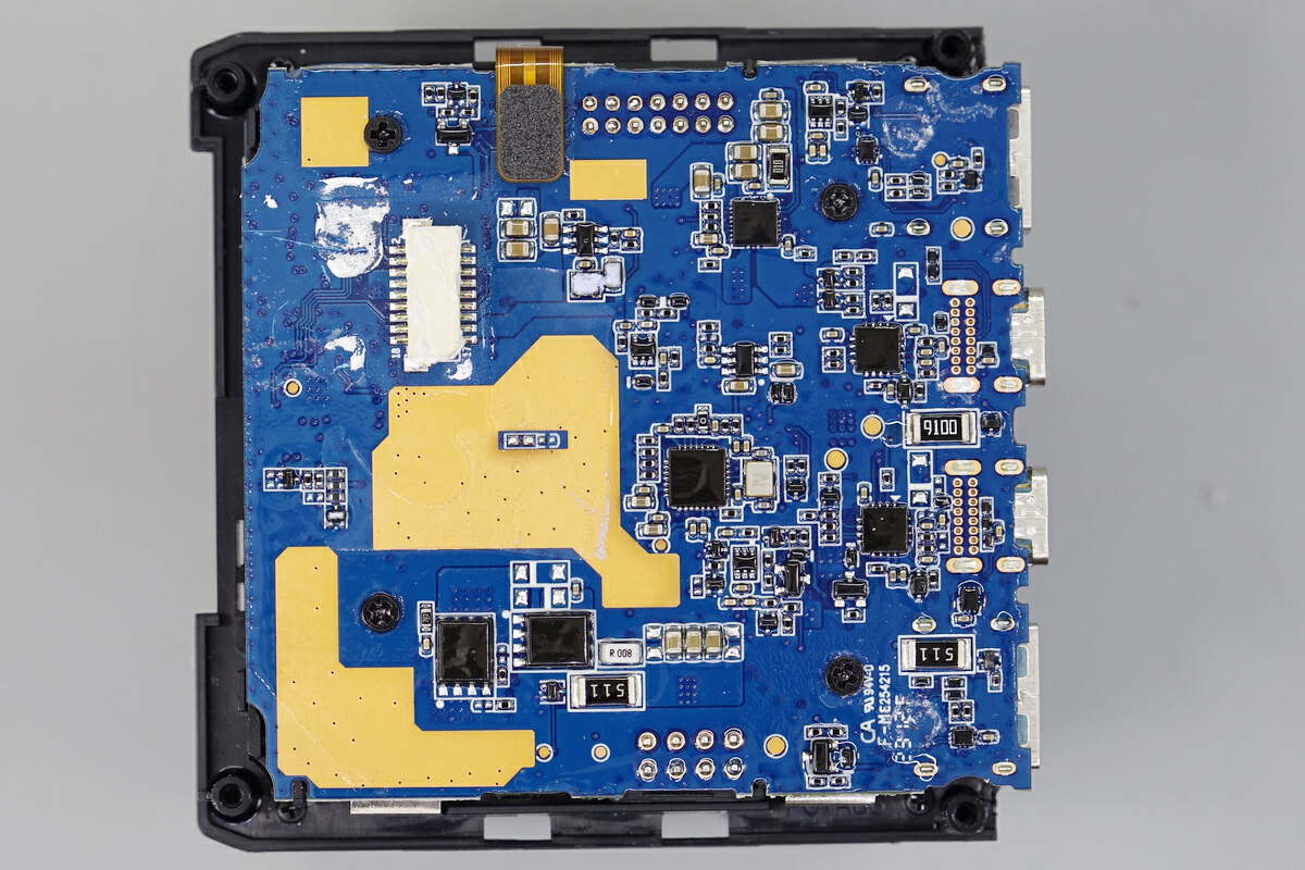
And the PCBA module is fixed inside the frame by screws.
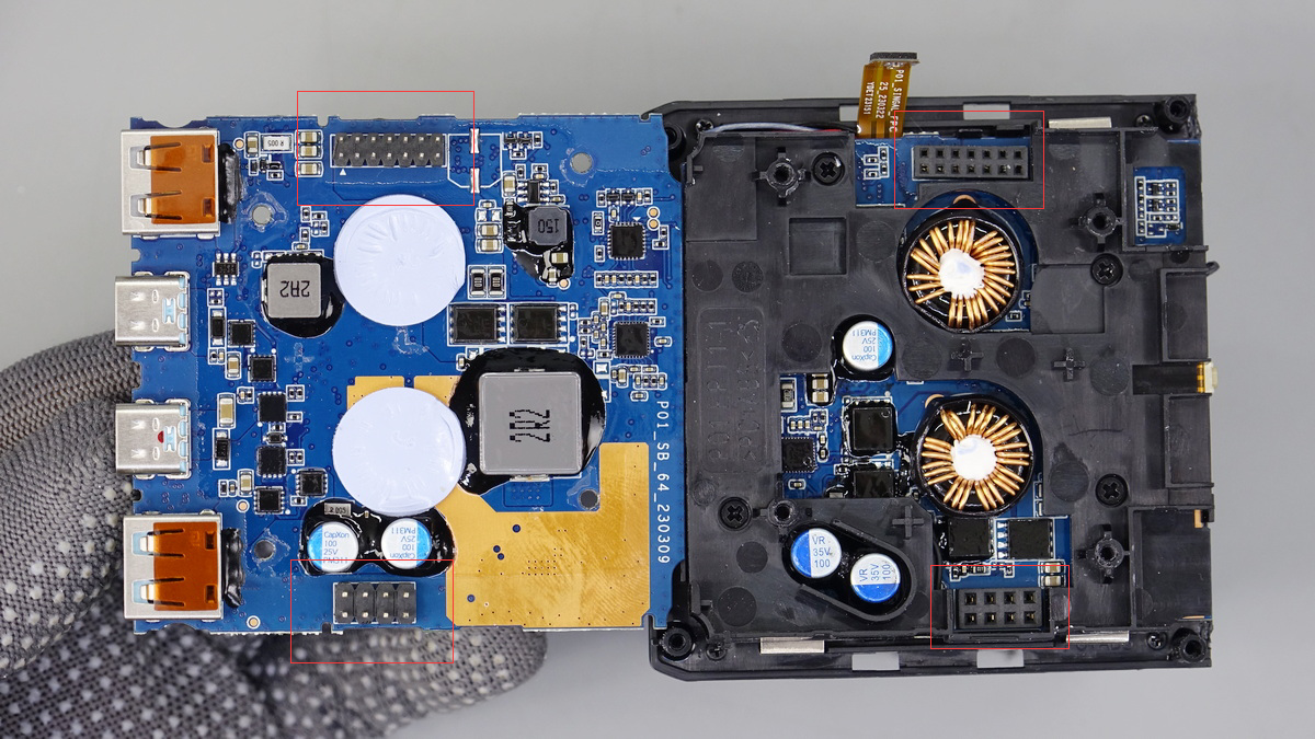
Then, separate those two parts. It consists of two layers, connected by two sets of pins for higher space utilization.
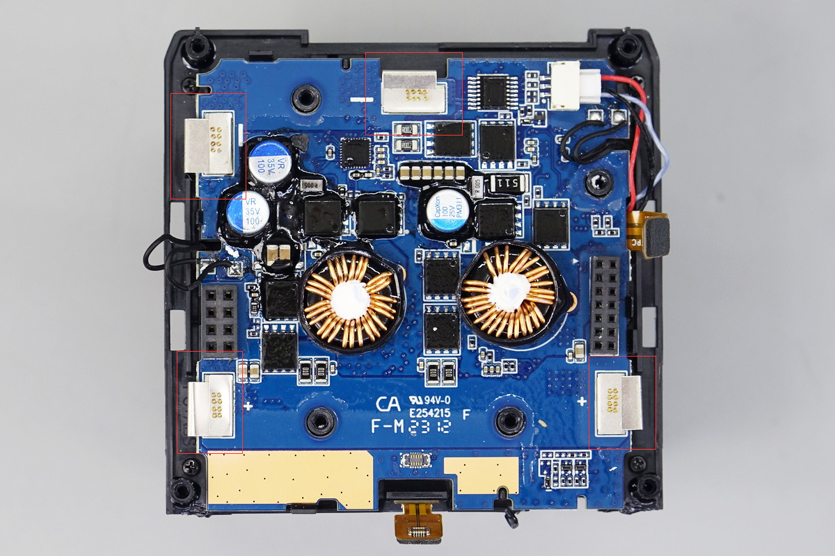
And nickel strips of the battery pack are connected to the lower PCB.
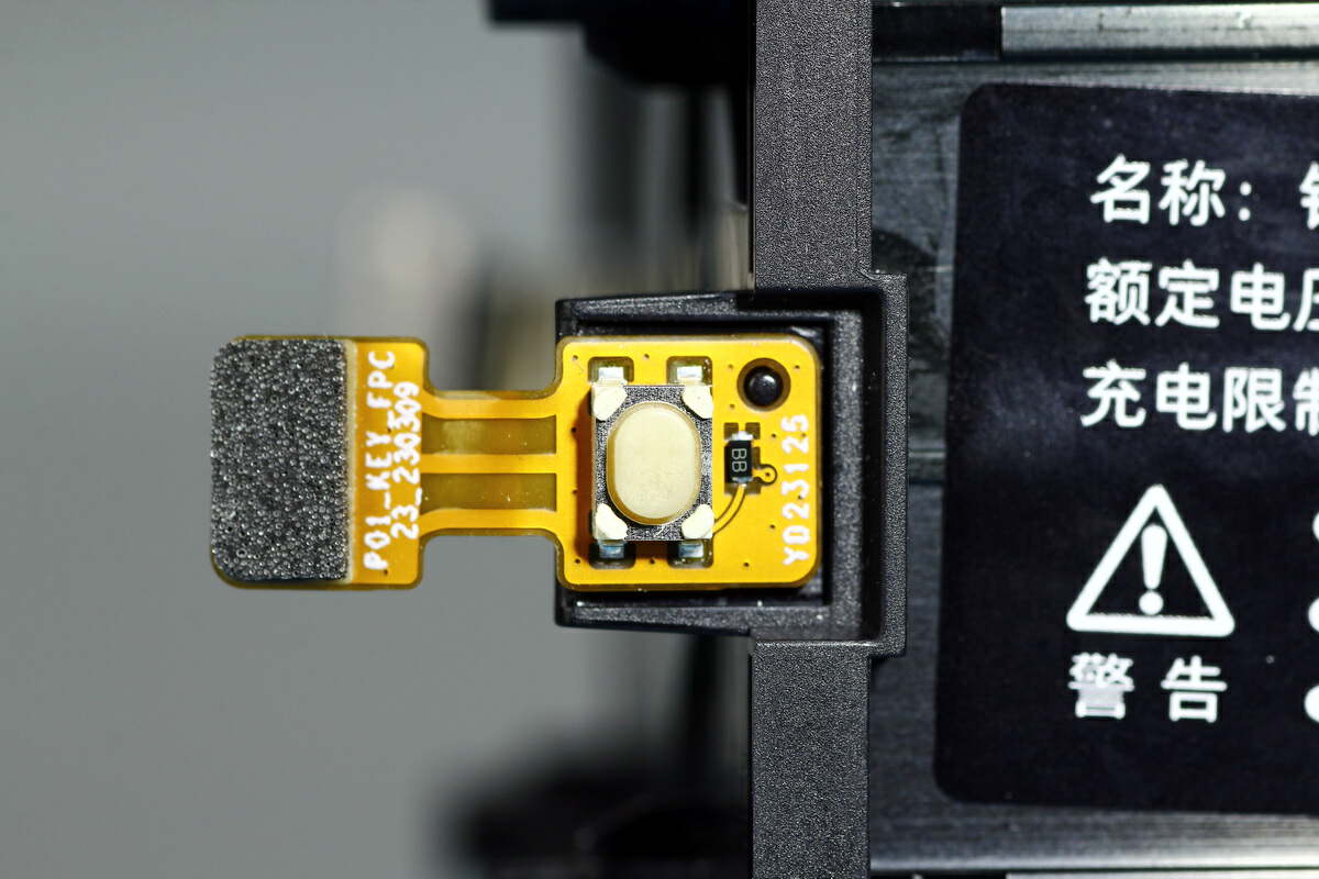
This is the power button, with a TVS for electrostatic protection.
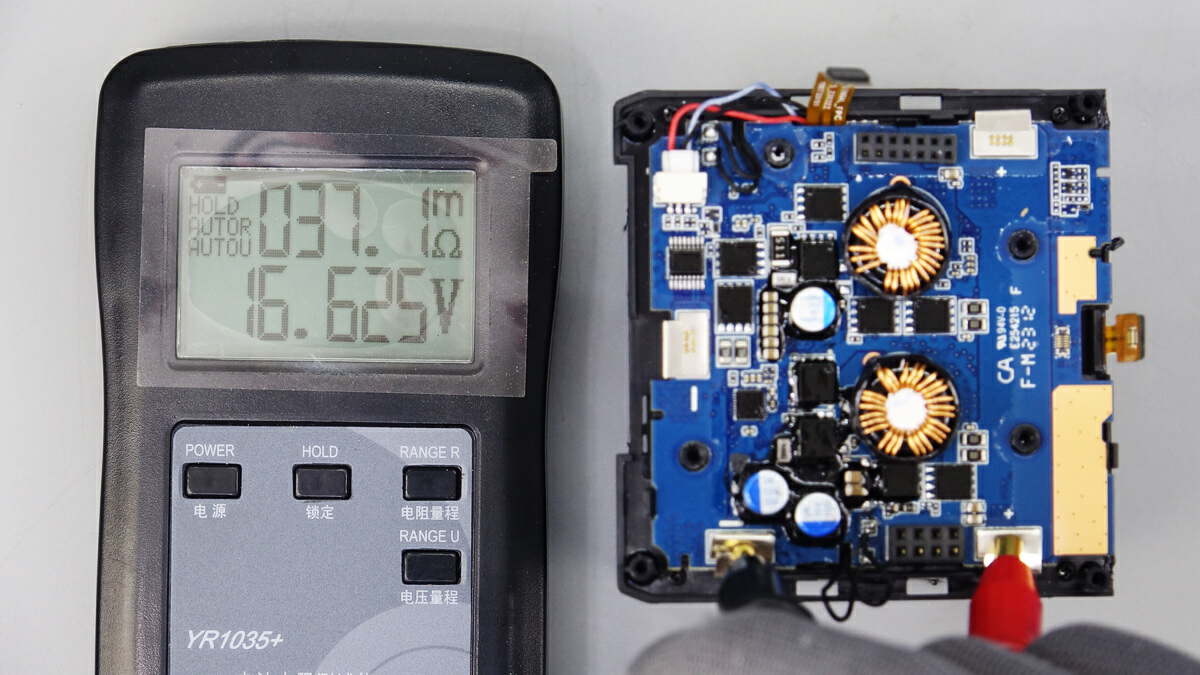
The voltage of the battery pack is about 16.6V.
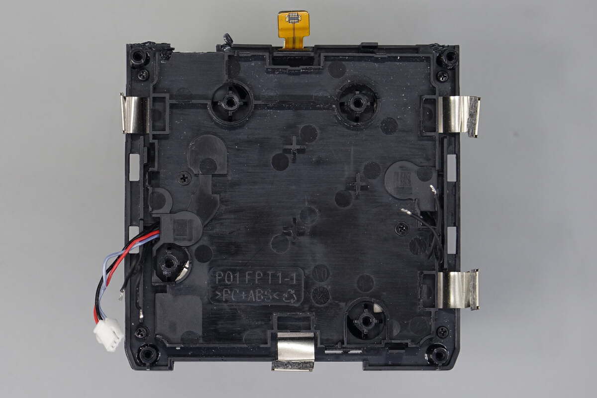
The lower PCB is also fixed in a black frame.
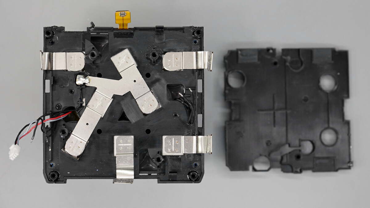
After removing it, we can see those nickel strips.
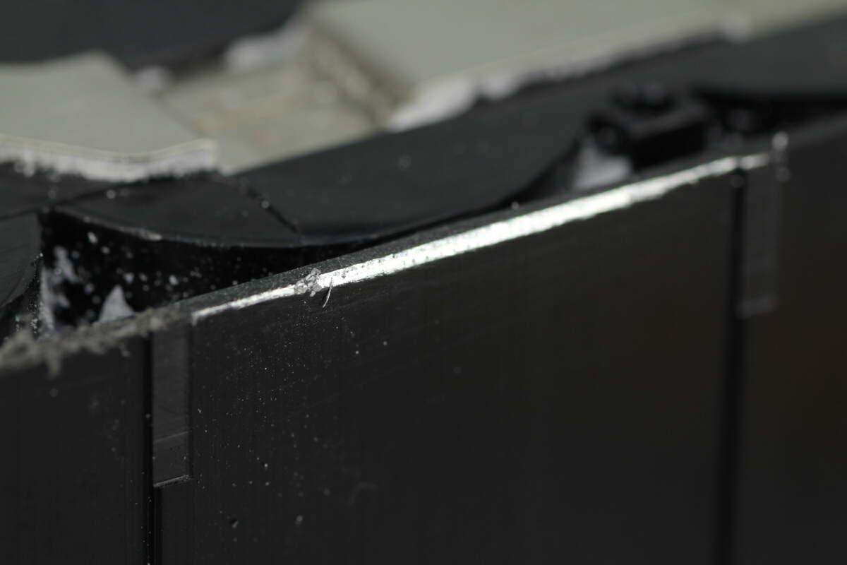
We even found the outer case adopts aluminum alloy after scraping off the black paint.
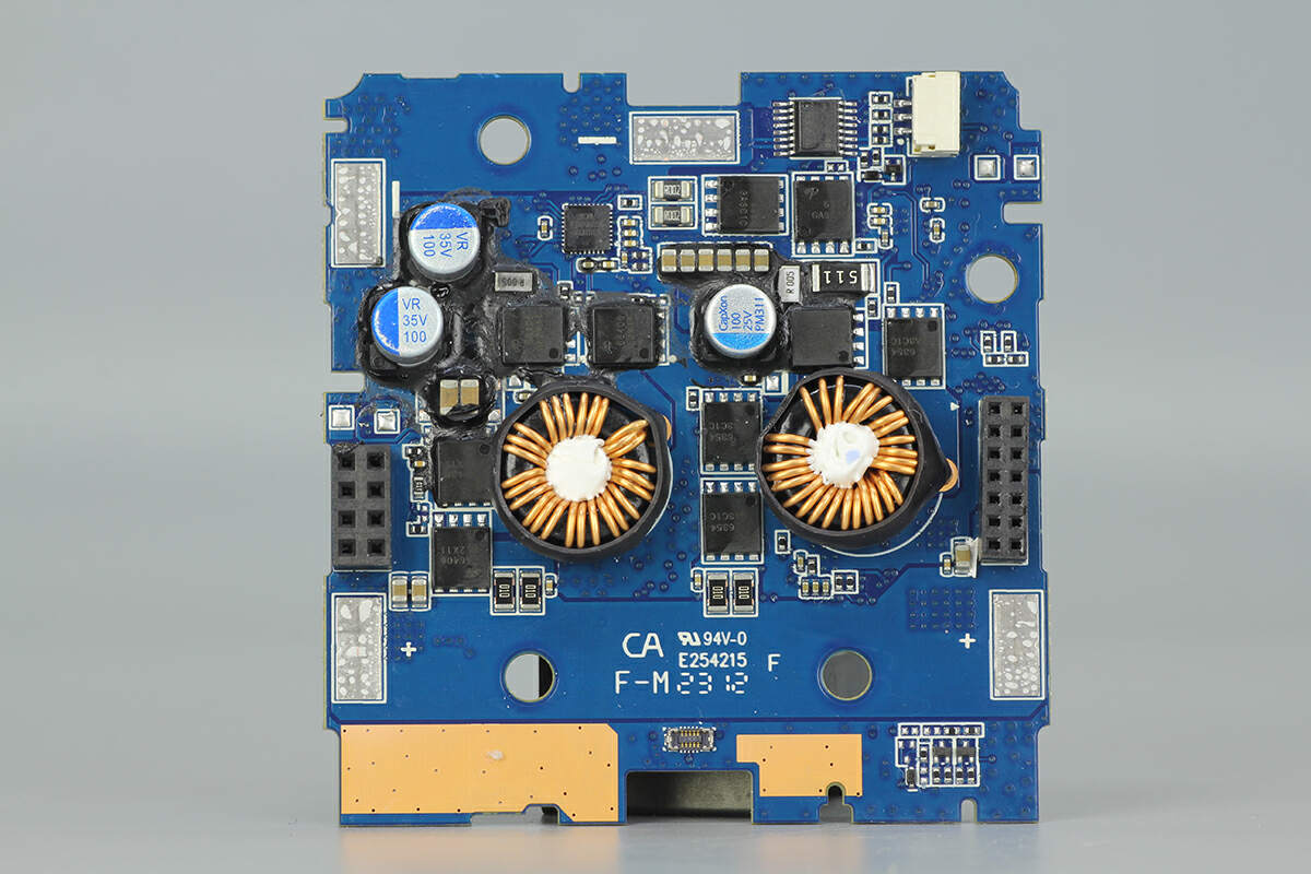
Then, let's go ahead and introduce all components one by one.
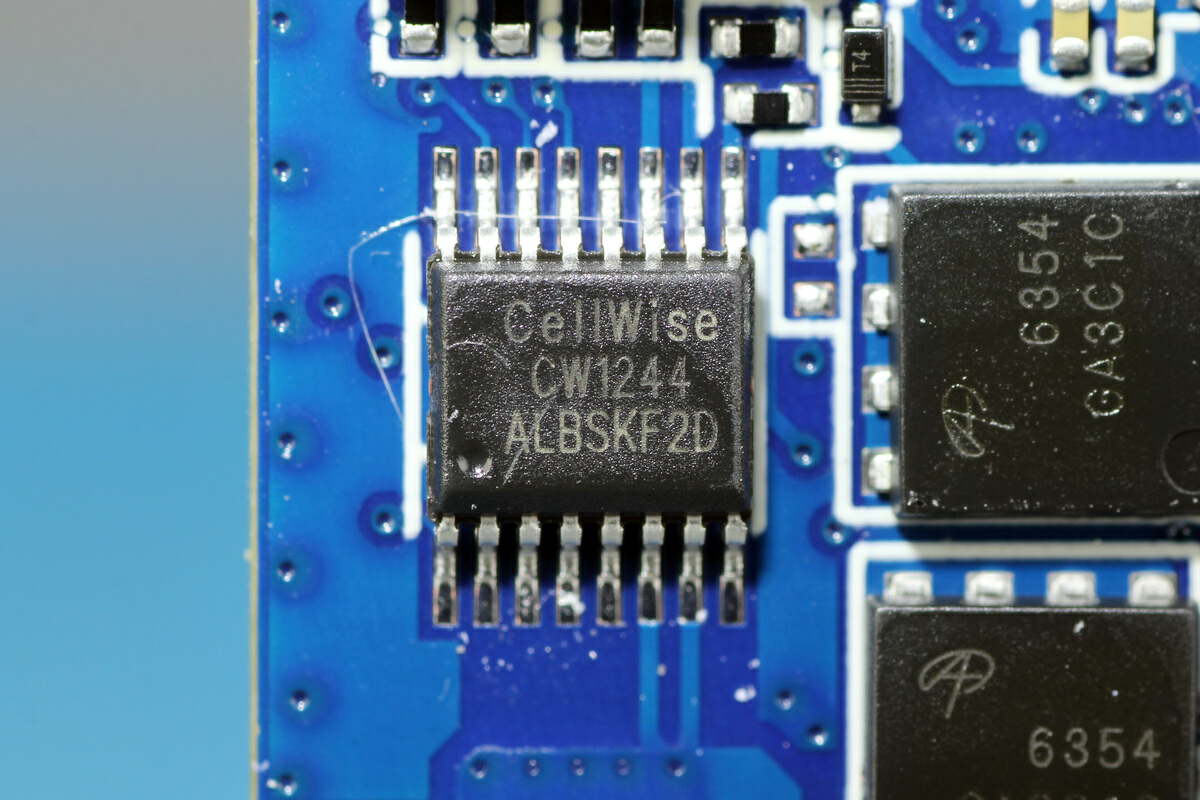
The battery protection chip is from Cellwise, model CW1244, which supports 3-4 lithium batteries connected in series and multiple battery protection functions.
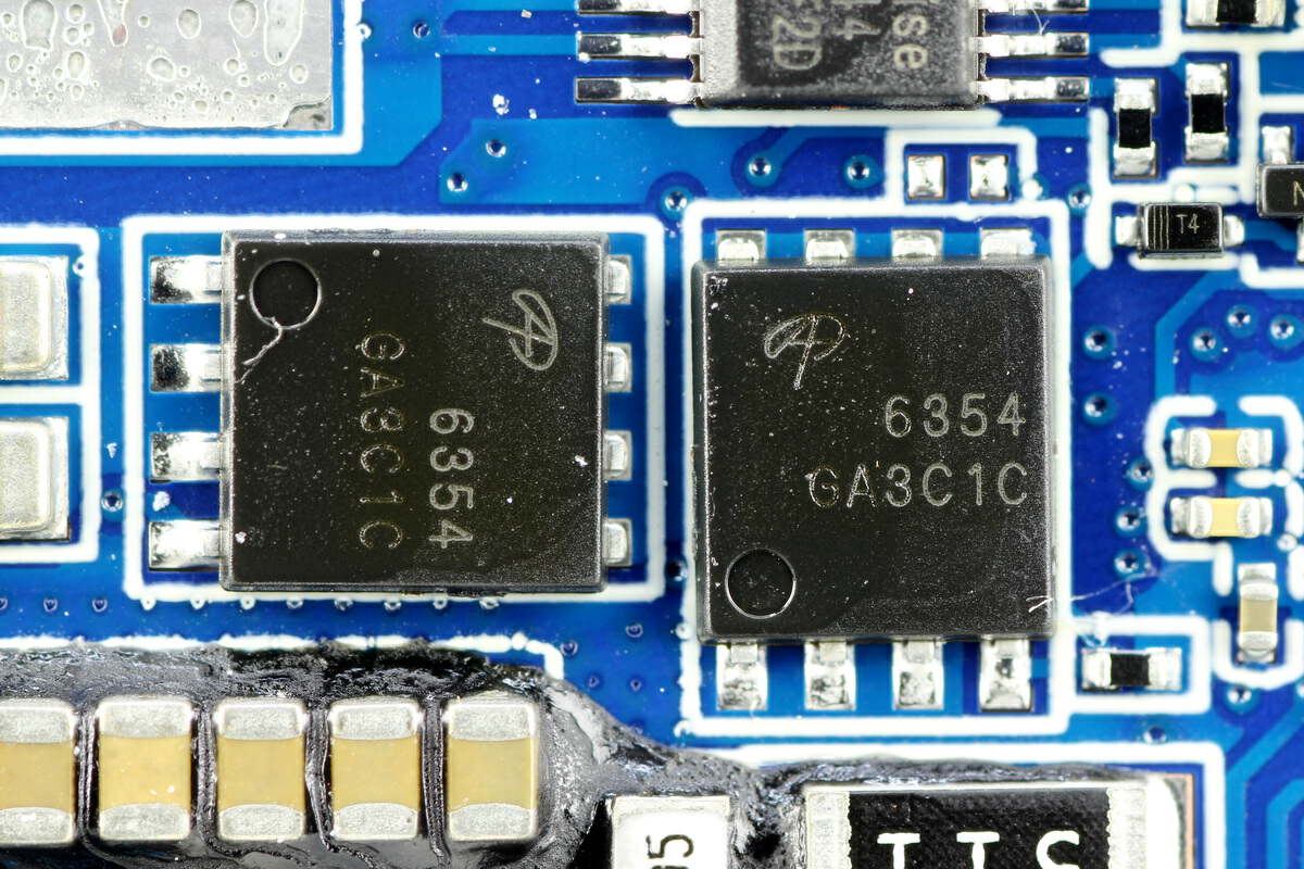
Those two MOSFETs for battery protection are from AOS and adopt DFN5 x 6 package. 30V, 2.75mΩ. Model is AON6354.
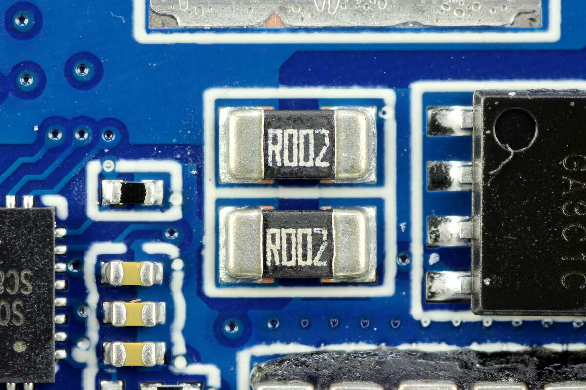
Two 2mΩ resistors are connected in parallel to detect the current of the battery pack.
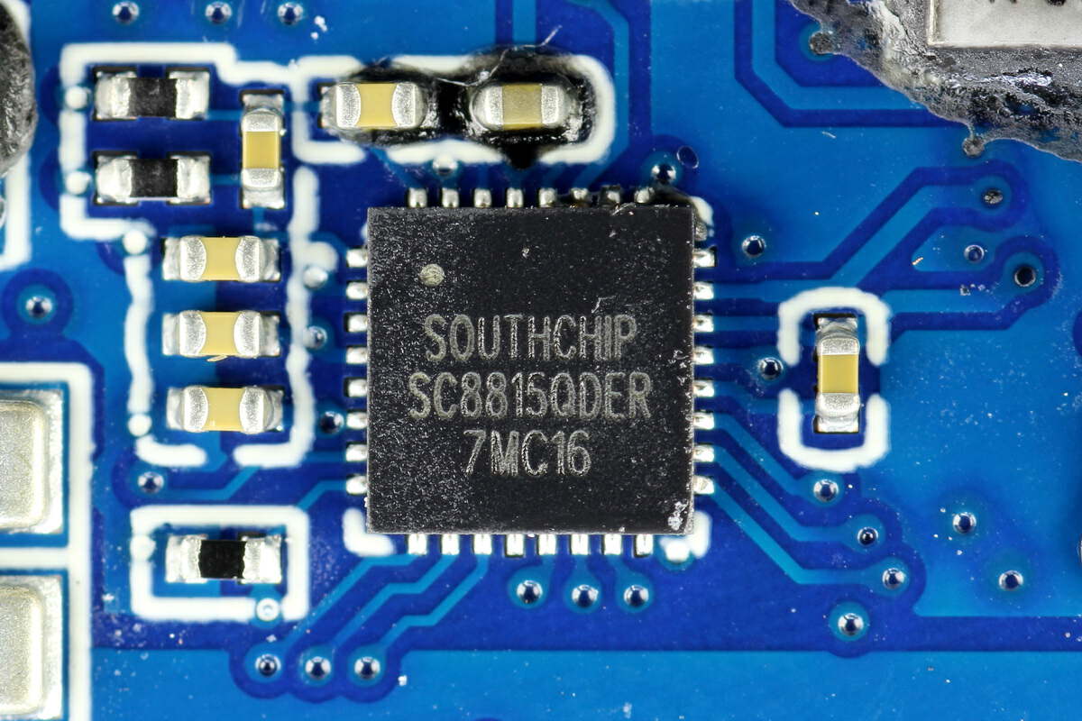
The buck-boost controller is from Southchip SC8815, used to convert DC input voltage. It can control the charging of the battery pack and USB-C output.
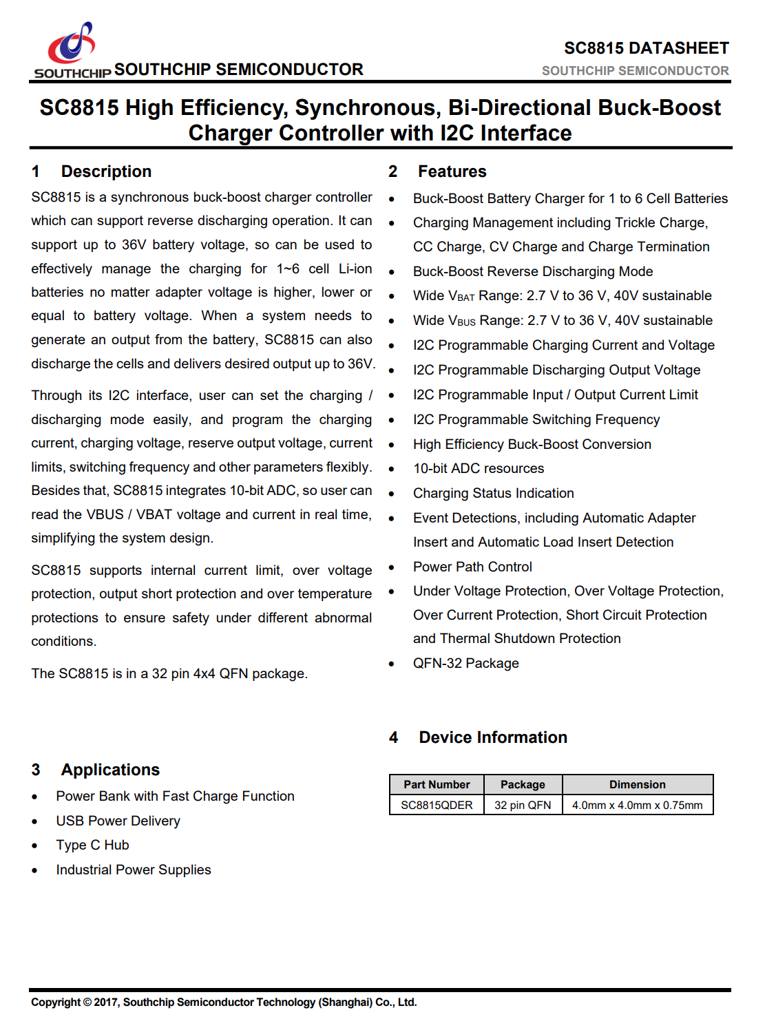
Here is all the information about the Southchip SC8815.
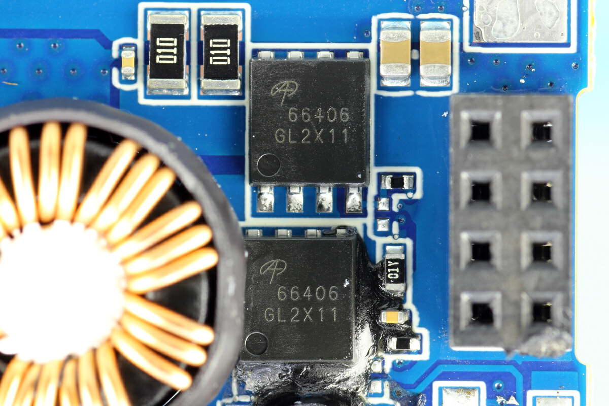
The synchronous buck-boost MOSFET is from AOS and adopts DFN5 x 6 package. 40V, 5mΩ. Model is AONS66406.
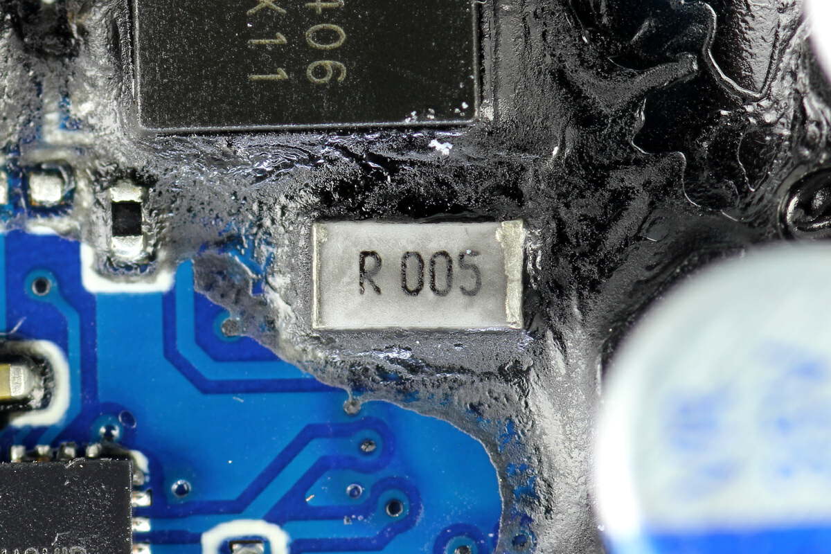
The 5mΩ resistor is used for current sensing while also providing overcurrent protection.
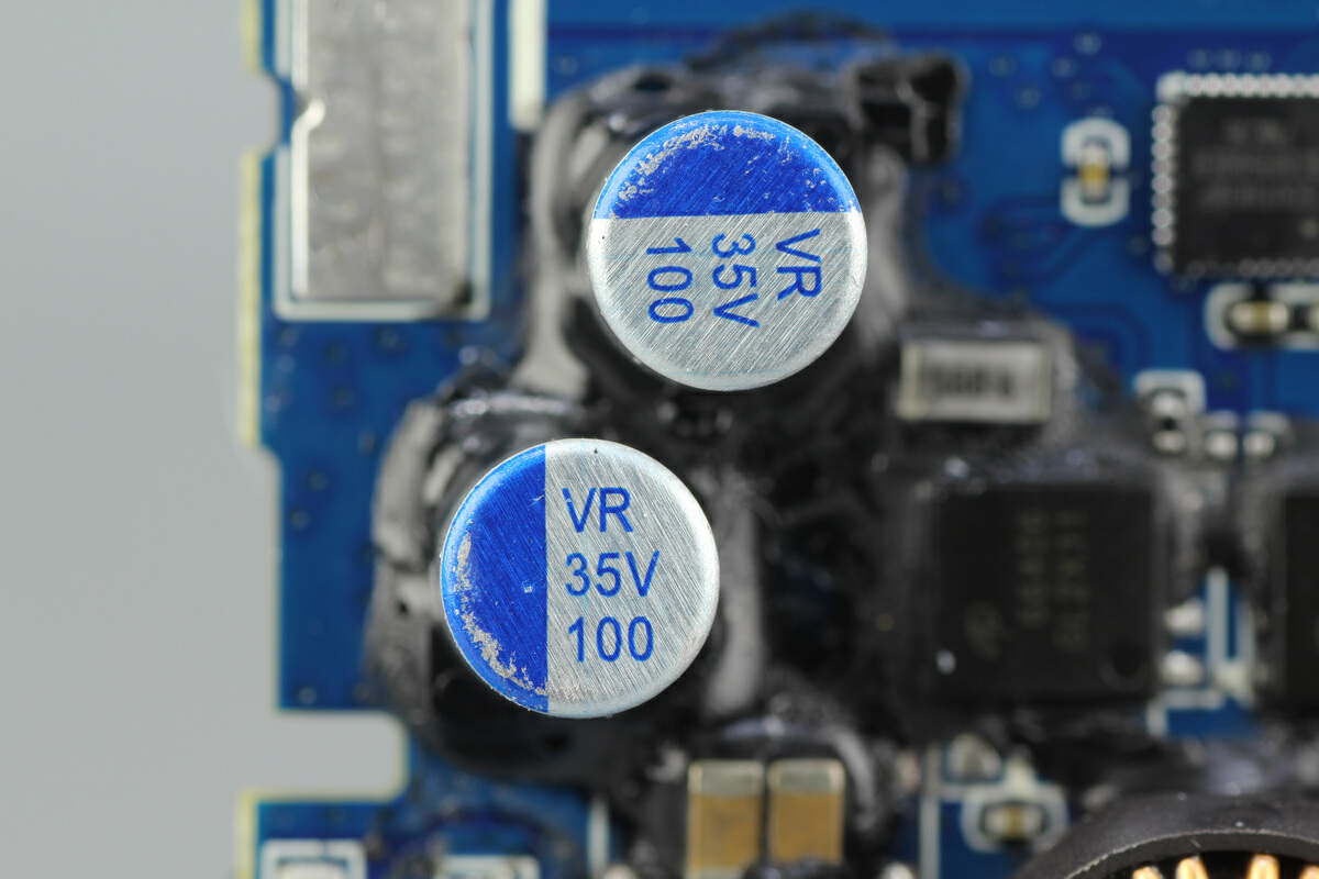
Those two solid capacitors for output filtering are connected in parallel, and used for the 140W output.
35V 100μF for each.
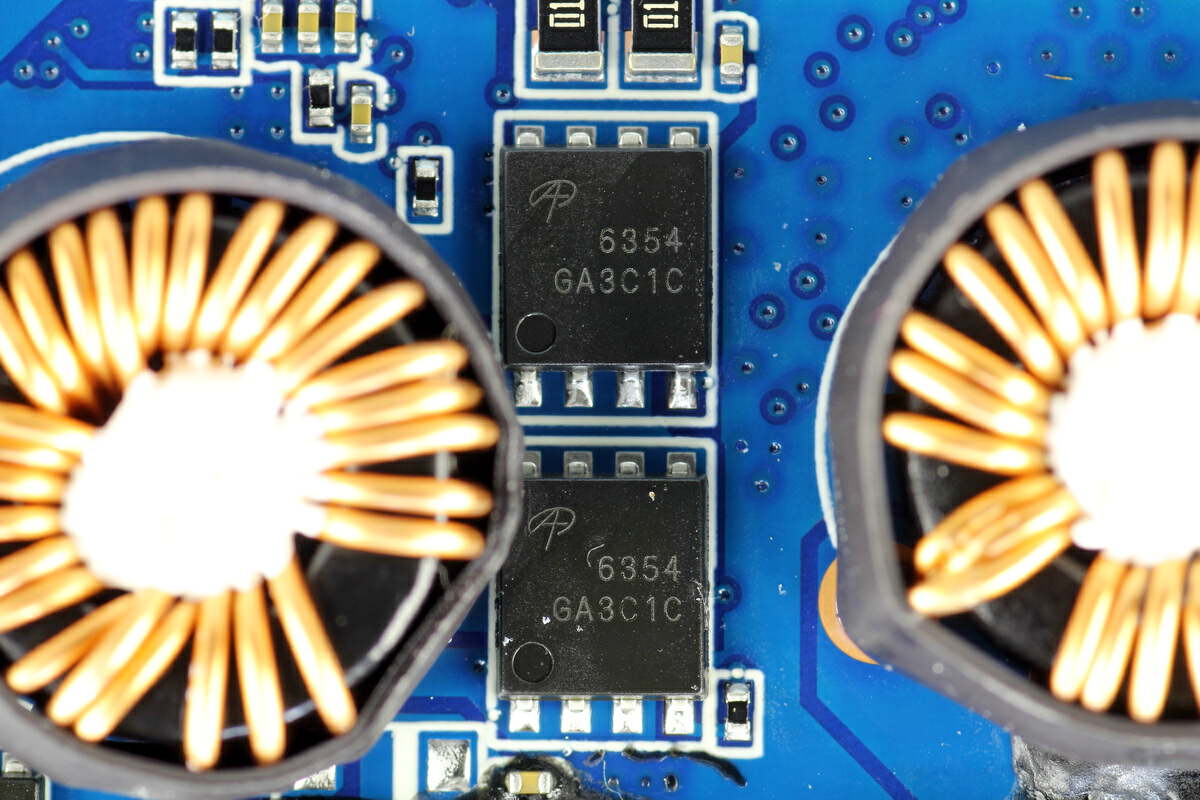
For the 100W output circuit, two MOSFETs for battery protection are the same model as the 140W circuit.
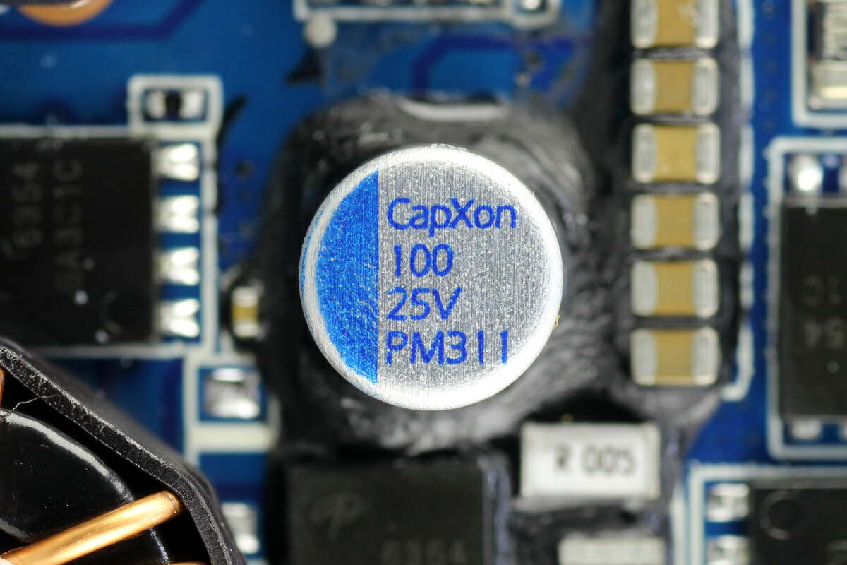
And this solid capacitor is from CapXon. 100μF 25V.
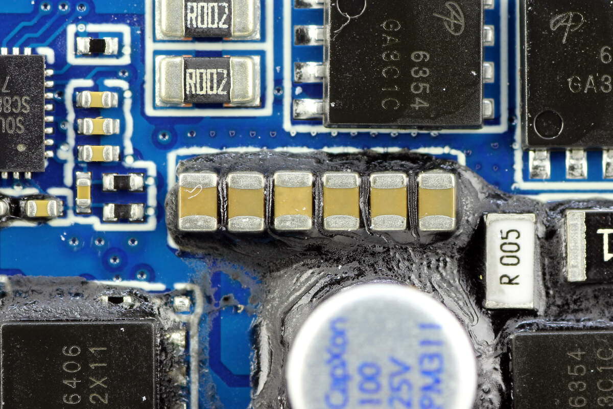
These six MLCC capacitors are connected in parallel.
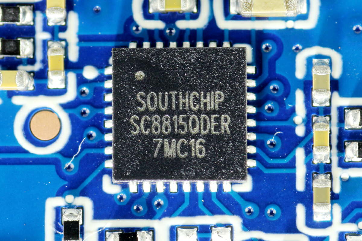
The buck-boost controller for 100W output is also from Southchip SC8815.
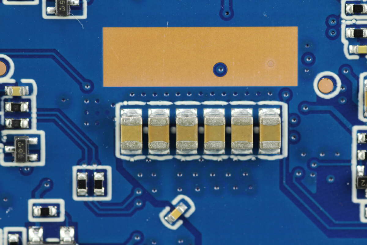
These six MLCC capacitors are yet again connected in parallel.
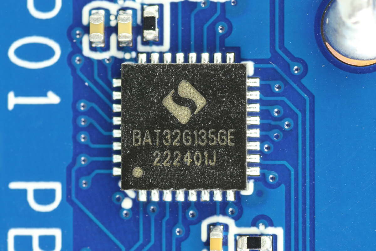
This MCU is from AMEC and adopts QFN32 package, used to drive the display. It can show the real-time battery capacity and input and output power. Model is BAT32G135GE32NA.
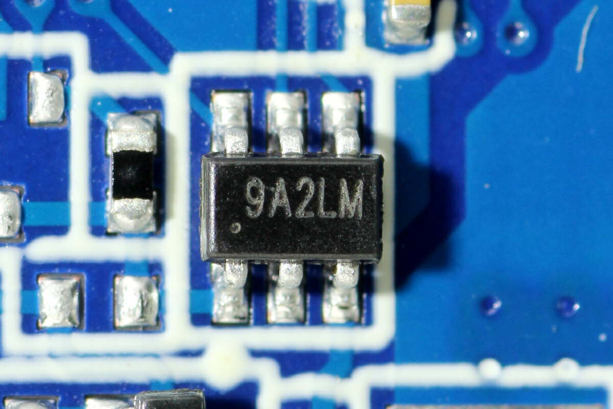
This current sense amplifier is from 3PEAK, used to detect the current of the buck-boost circuit. Model is TP199A2.
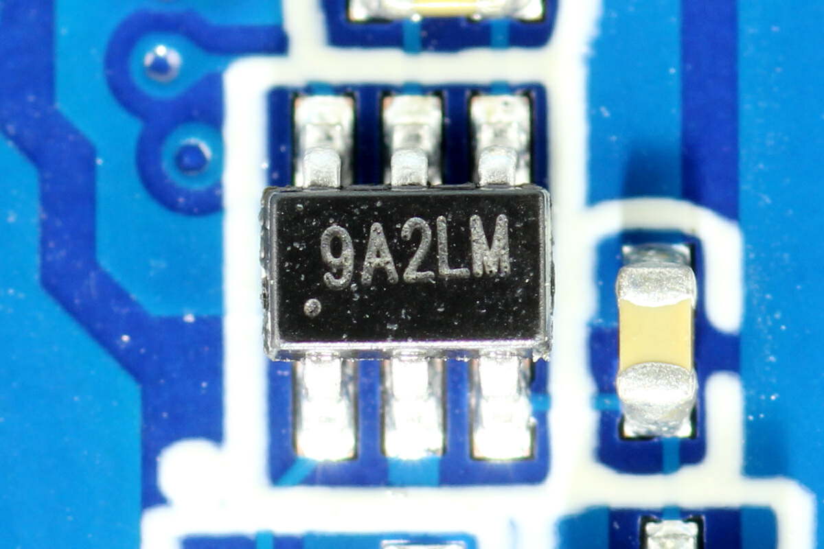
And here is another same one, which is used for another buck-boost circuit.
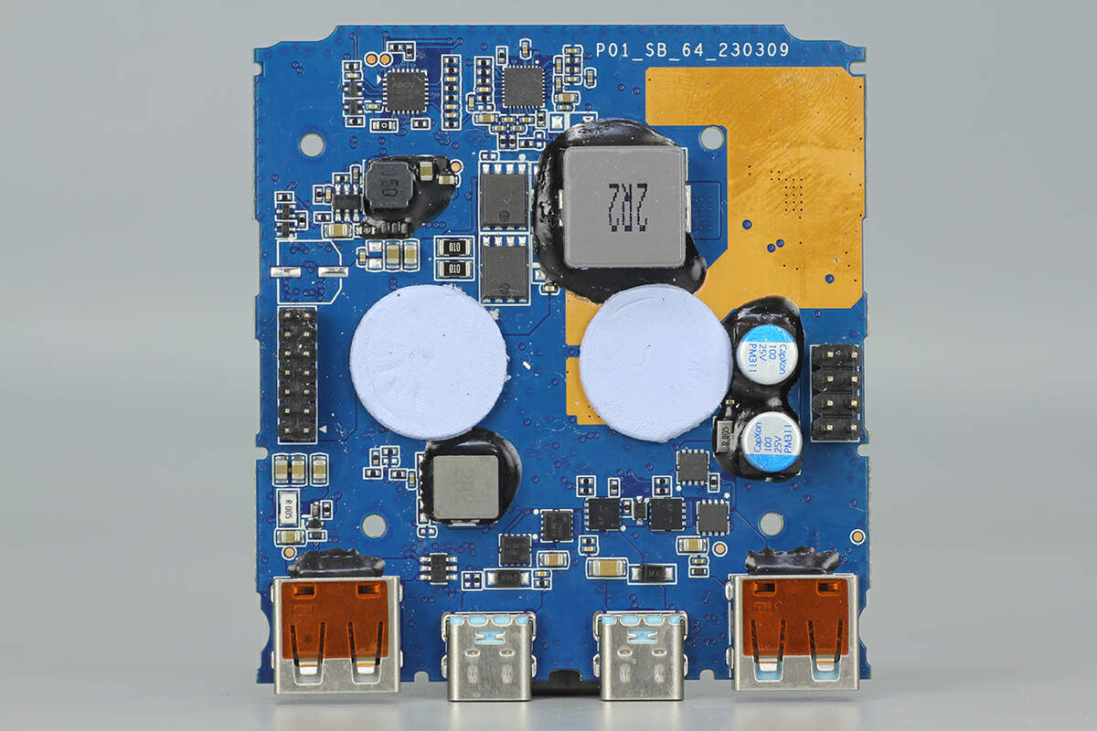
Next, let's move on to another PCB, which has two synchronous buck-boost circuits for the outputs of two USB-A ports.
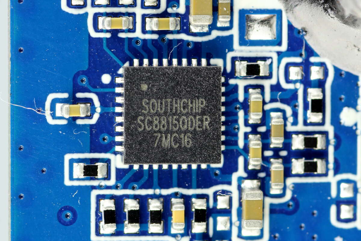
The synchronous buck-boost controller for the 120W USB-A output is also from Southchip SC8815. It has three chips of SC8815 in total.
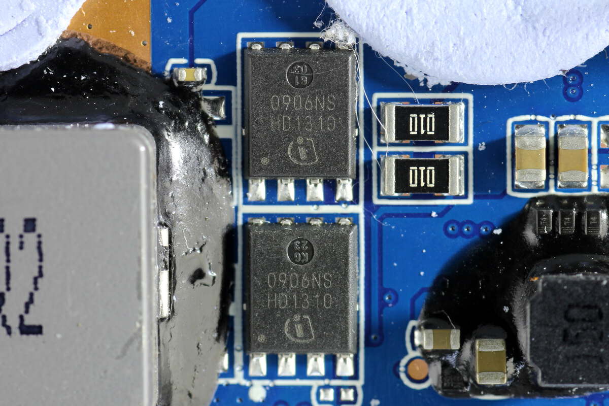
Those two MOSFETs are from Infineon. 30V, 4.5mΩ. Model is BSC0906NS.
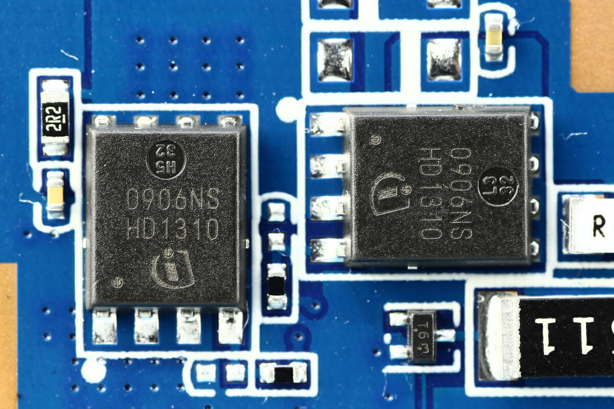
And there're two same MOSFETs on the back.
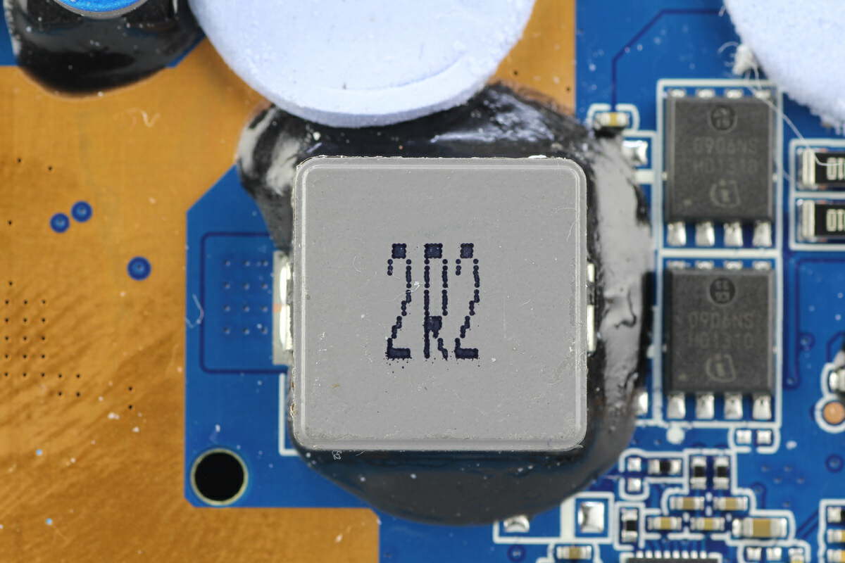
The 2.2μH alloy inductor is used for the buck-boost conversion of 120W USB-A output.
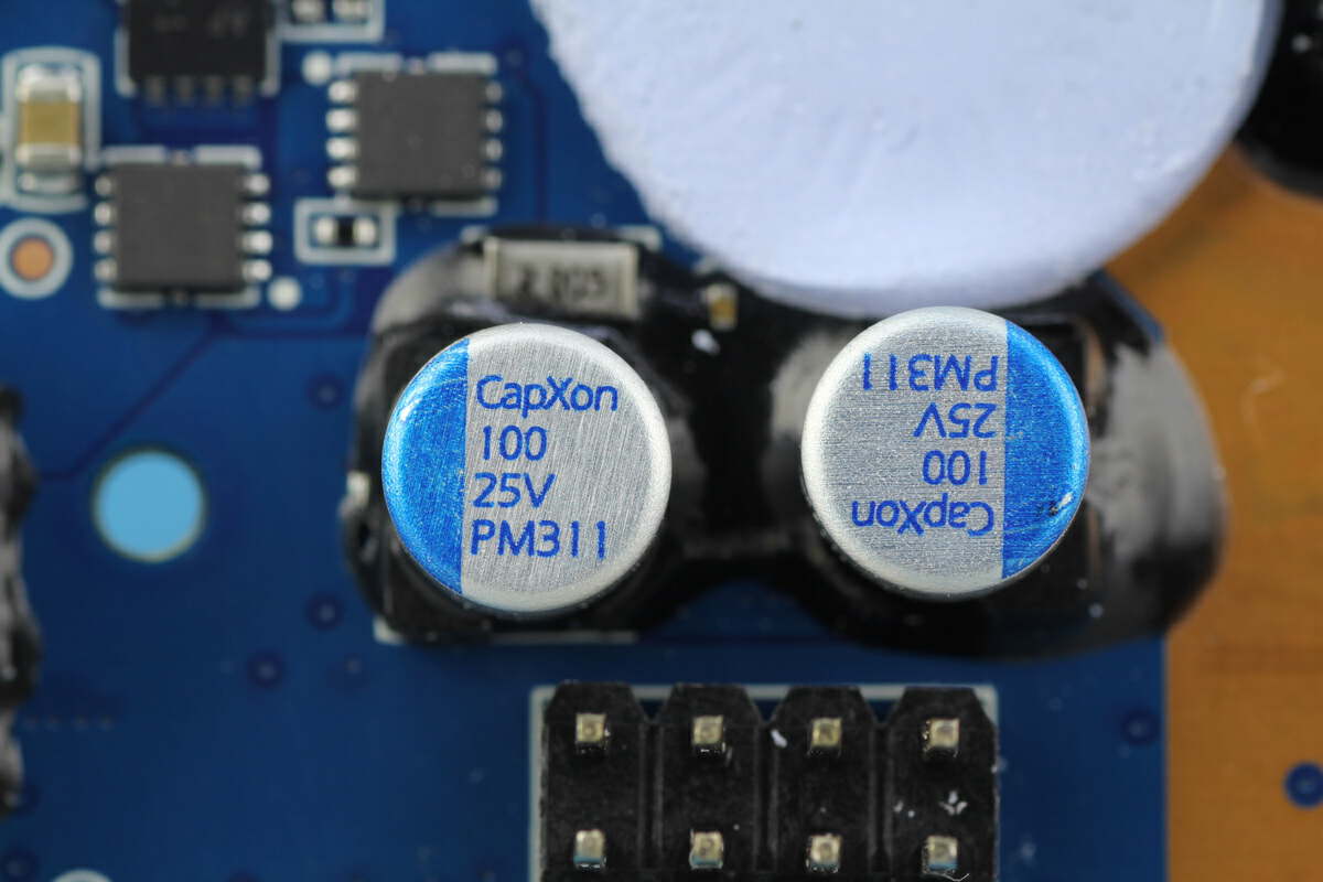
Those two solid capacitors are from CapXon PM series. 100μF 25V for each.
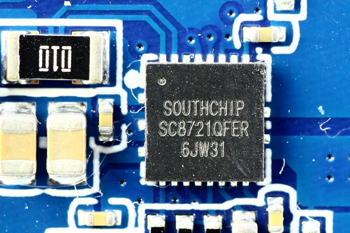
The synchronous buck-boost converter for the other 22.5W USB-A is different from the other three ports, from Southchip SC8721. It integrates four buck-boost MOSFETs to form an H-bridge, the input and output voltage is between 2.7-22V. It also supports wide input and output voltage range.
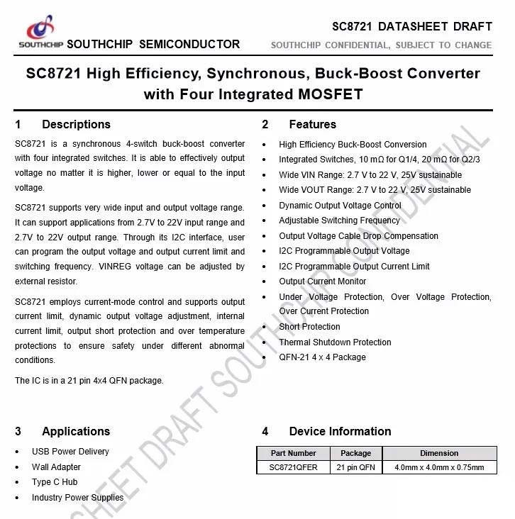
Here is all the information about Southchip SC8721.
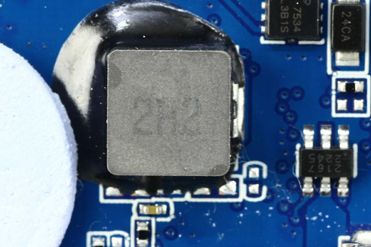
This buck-boost inductor is used for the 22.5W USB-A.
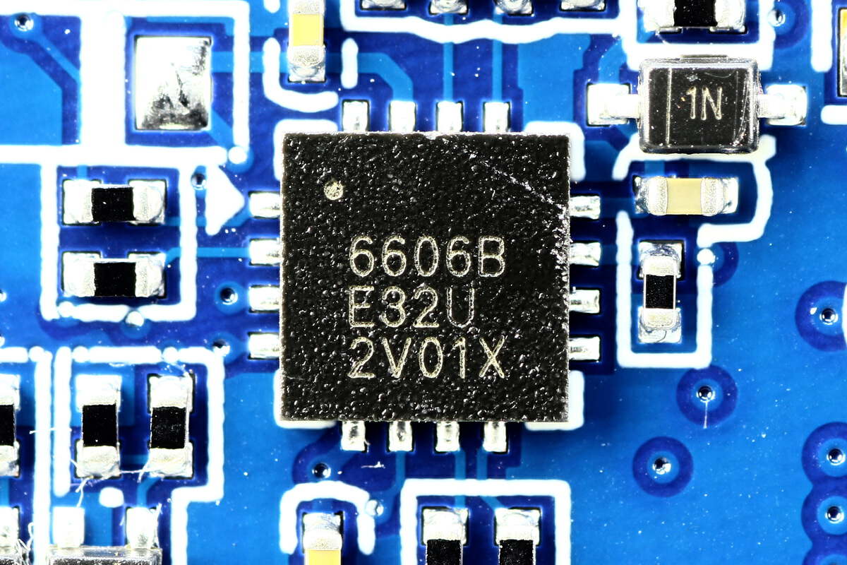
Two protocol chips of two USB-C ports are from Jadard FP6606 and adopt TQFN-24 and TQFN-16 packages. We also found a similar chip in the teardown video of Anker 140W PD3.1 power bank.
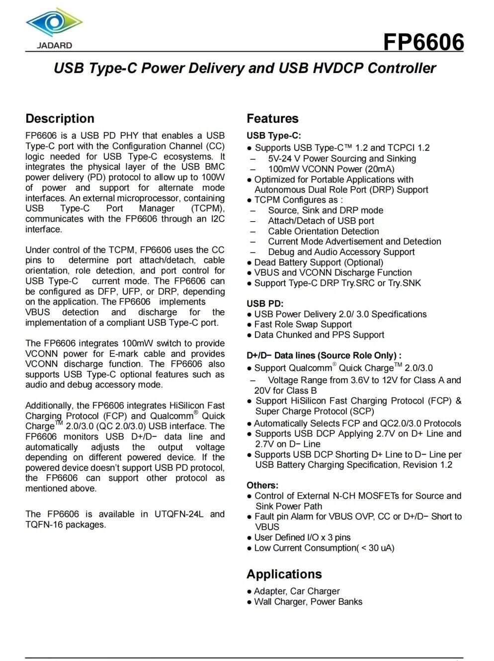
Here is all the information about Jadard FP6606.
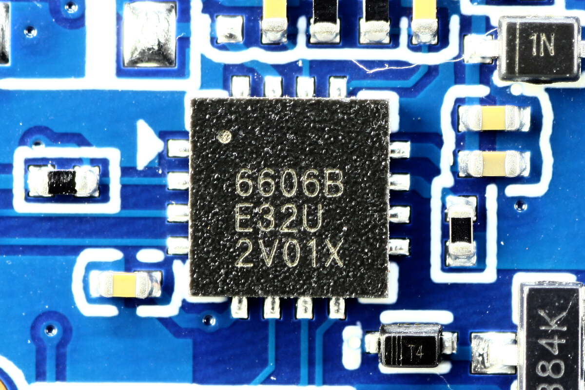
And here is the other one.
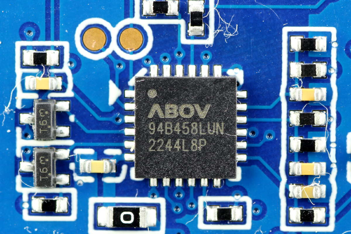
The MCU is from ABOV, used to control different functions of this power bank. Model is A94B458LUN.
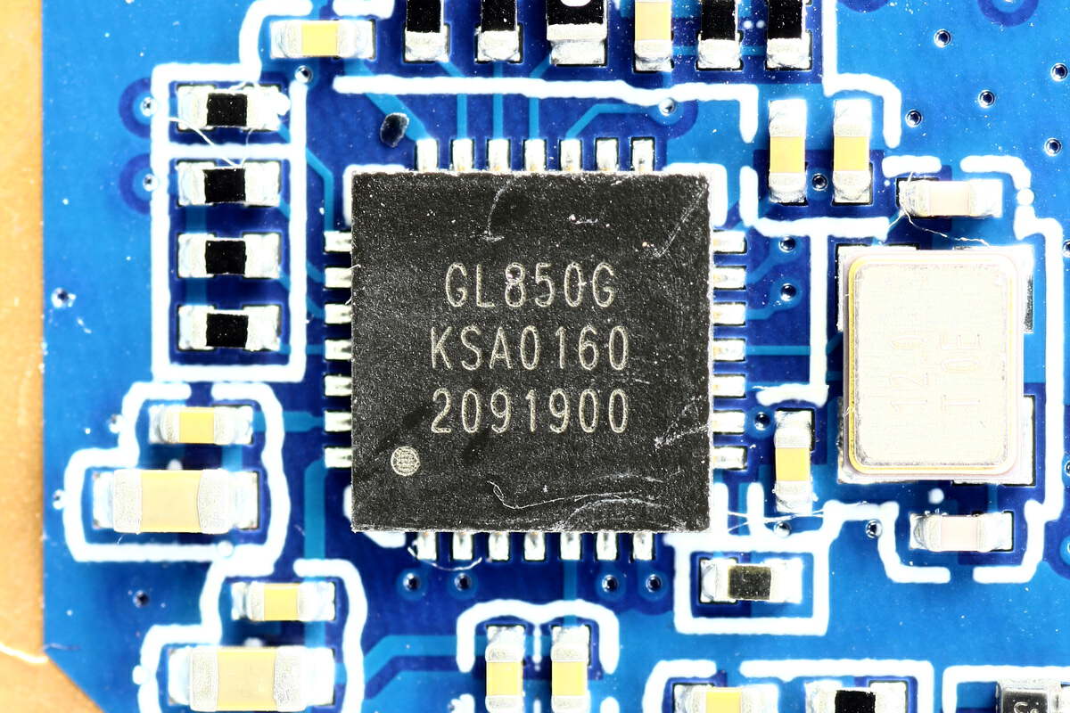
The USB hub controller is from Genesys, used for the expansion of USB ports. Model is GL850G.
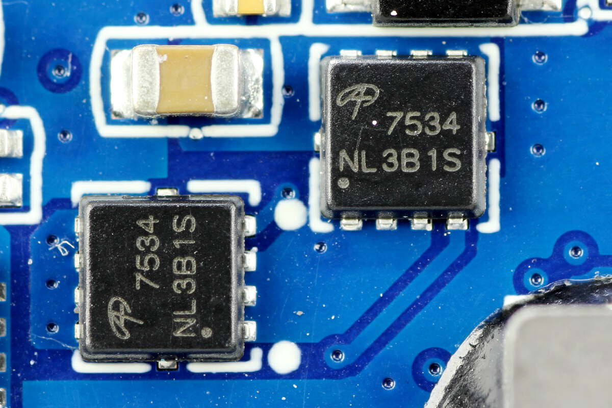
Those two VBUS MOSFETs for USB-C output are from AOS. Model is AON7534.
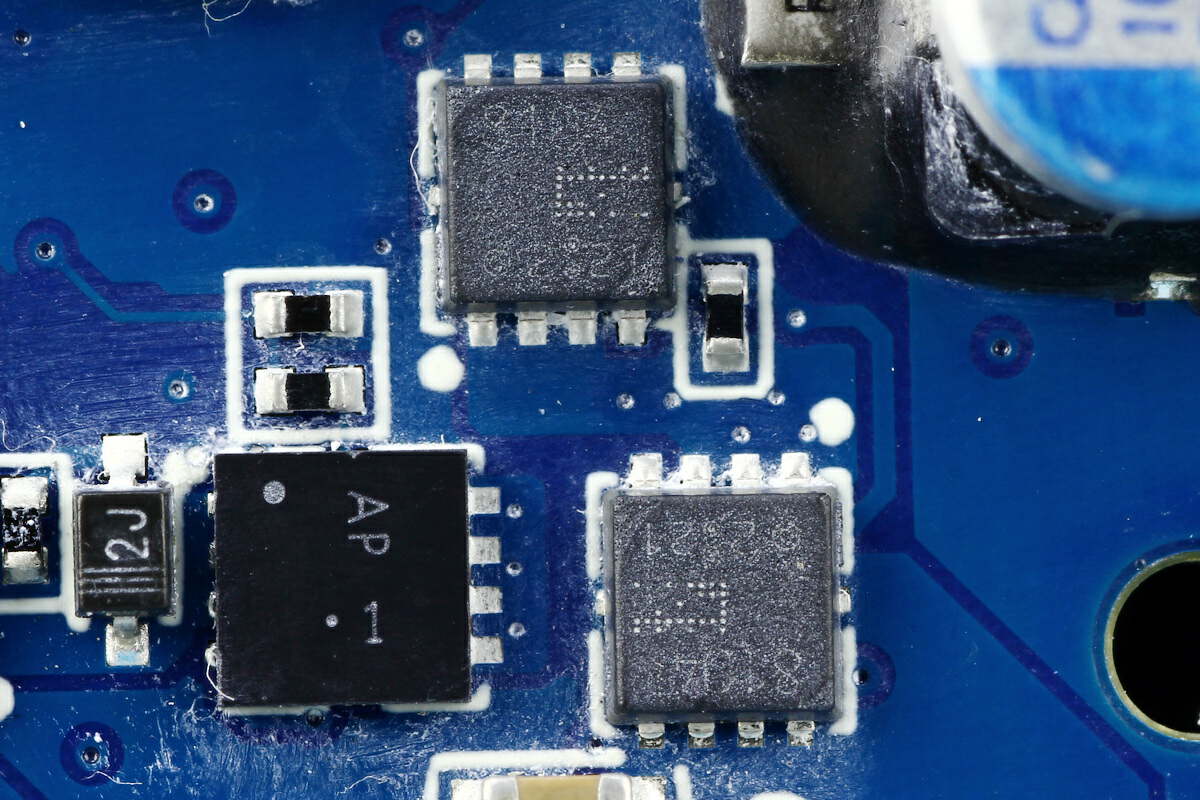
The other two VBUS MOSFETs for 120W USB-A output are from Toshiba. Model is TPCC8104.
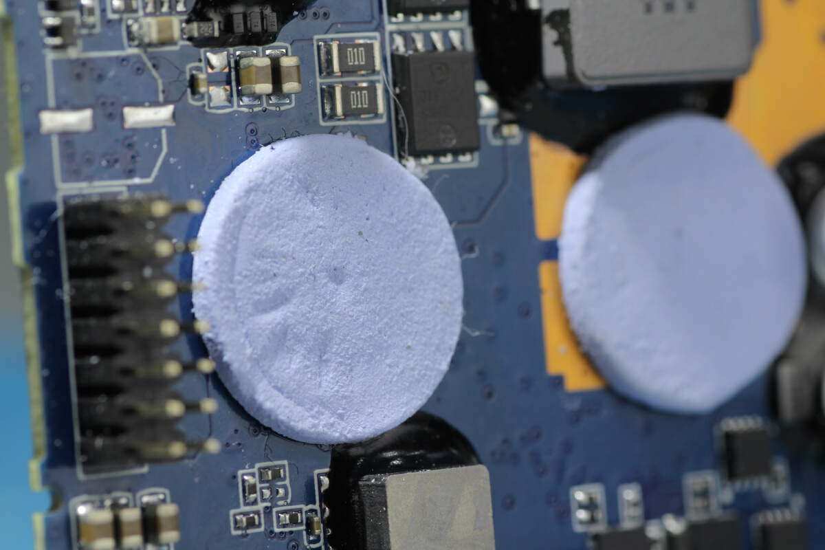
These two thermal pads are used for heat dissipation of the toroidal core inductor in another PCB.
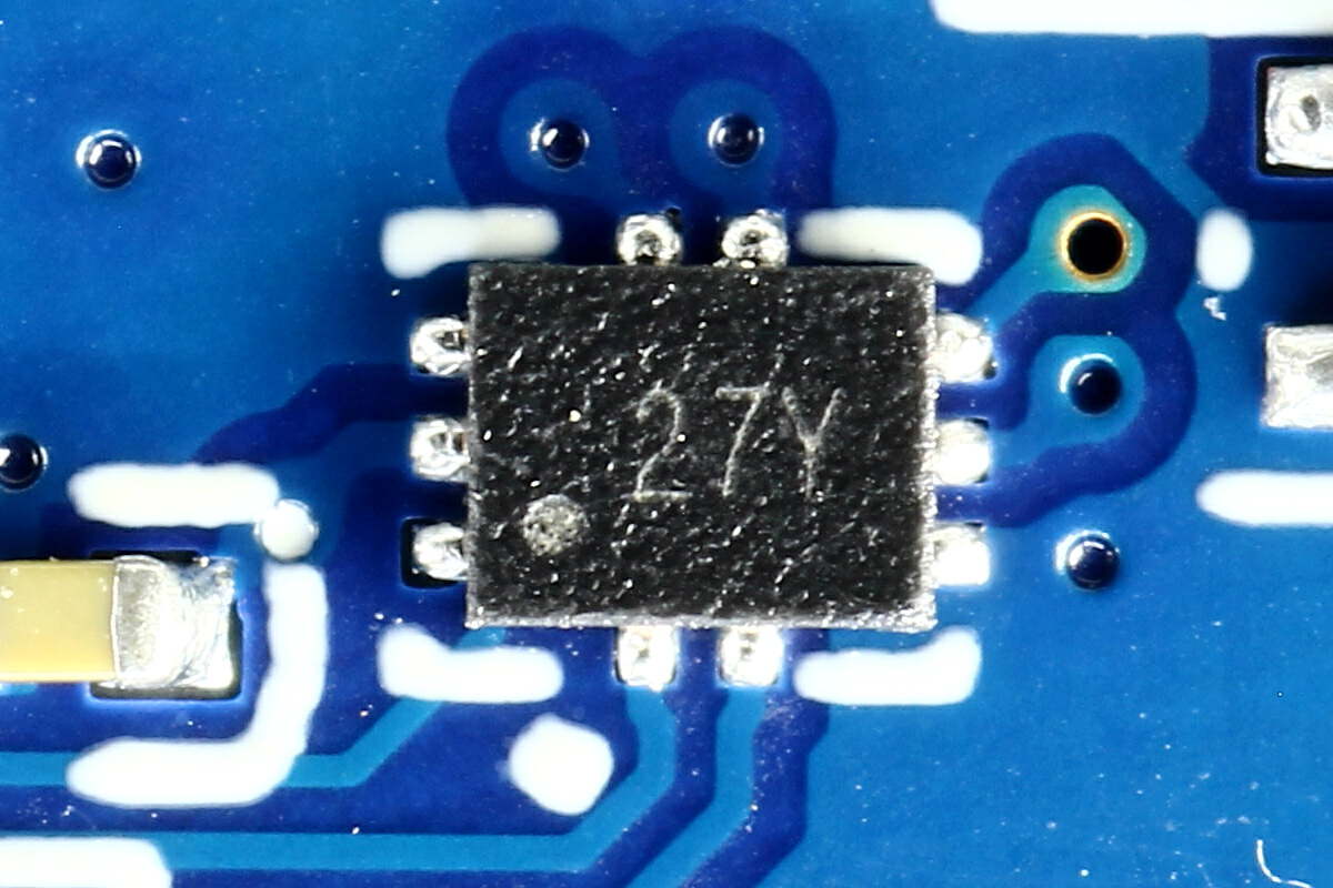
The switch with "27Y" printed on it is used to switch between various protocols of the USB-A port.
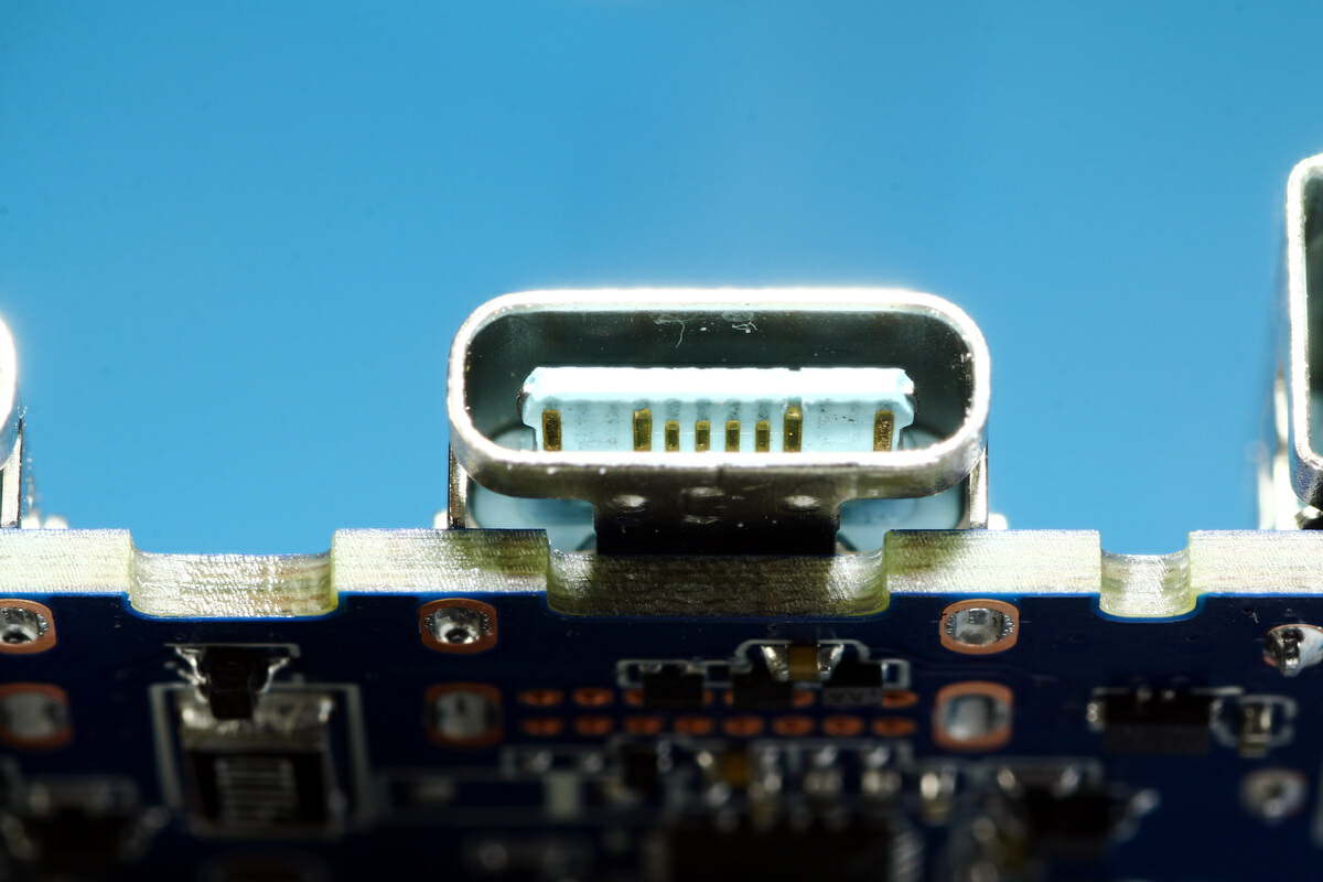
The plastic sheet inside the USB-C socket is blue.
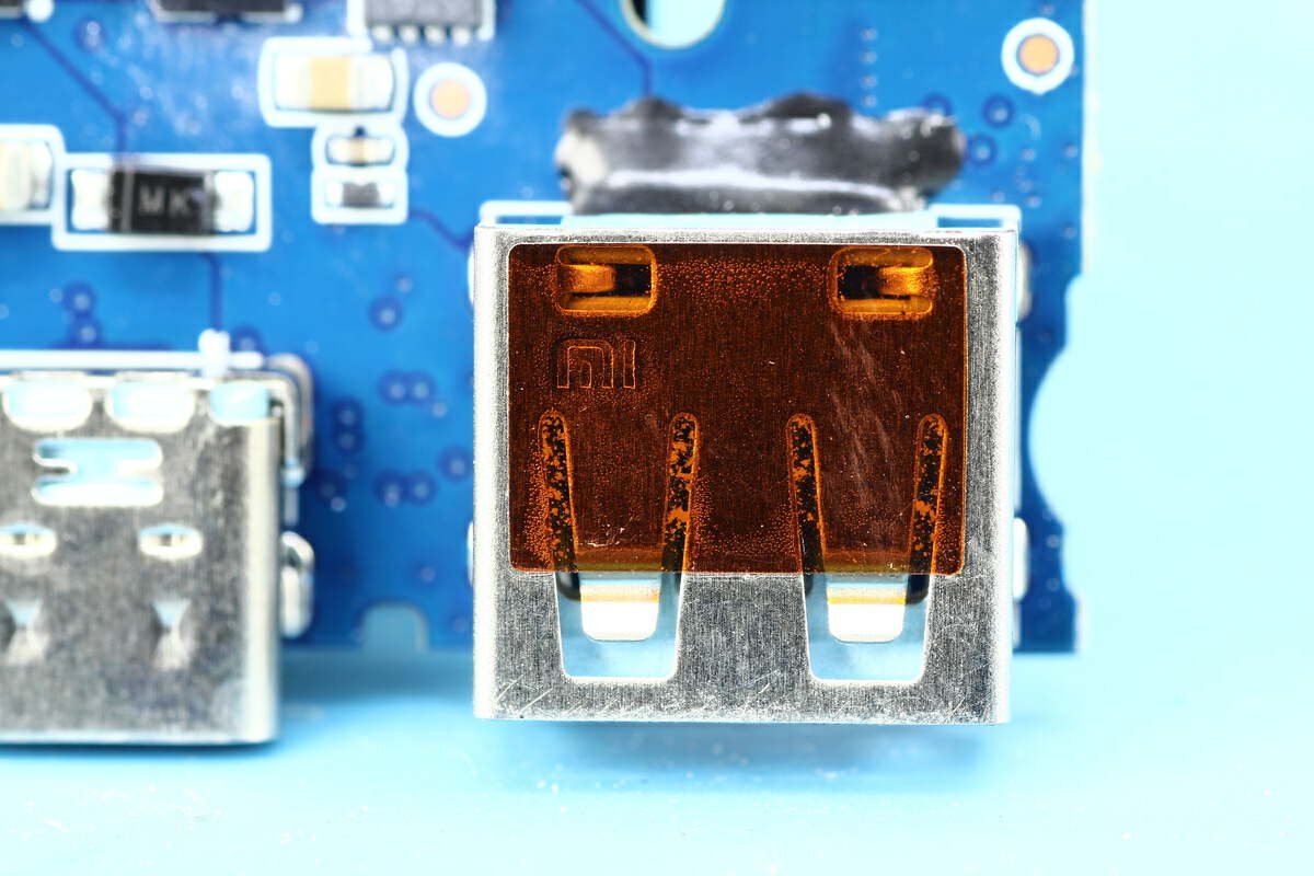
The USB-A socket is engraved with the letters "MI," which resembles the logo of Xiaomi. However, we cannot confirm anything, and we leave it to you to make your own judgment.
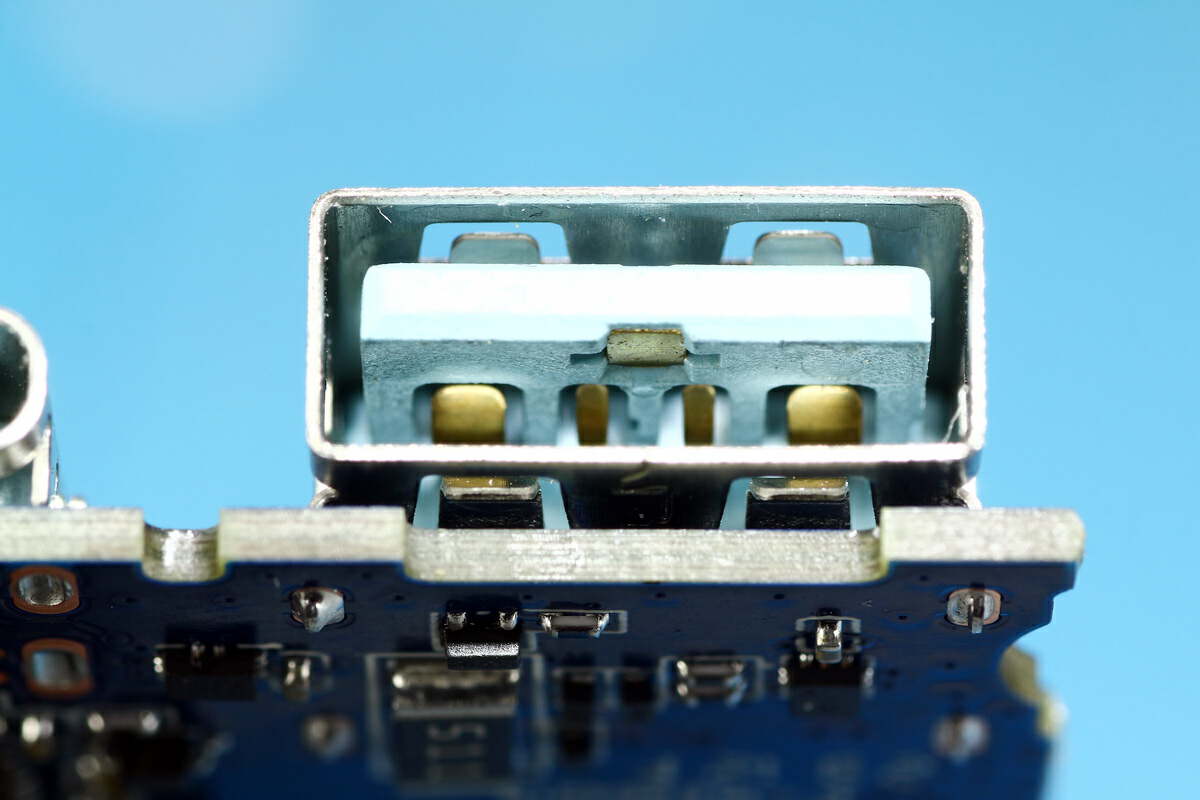
And the plastic sheet inside the 120W USB-A socket is also blue.
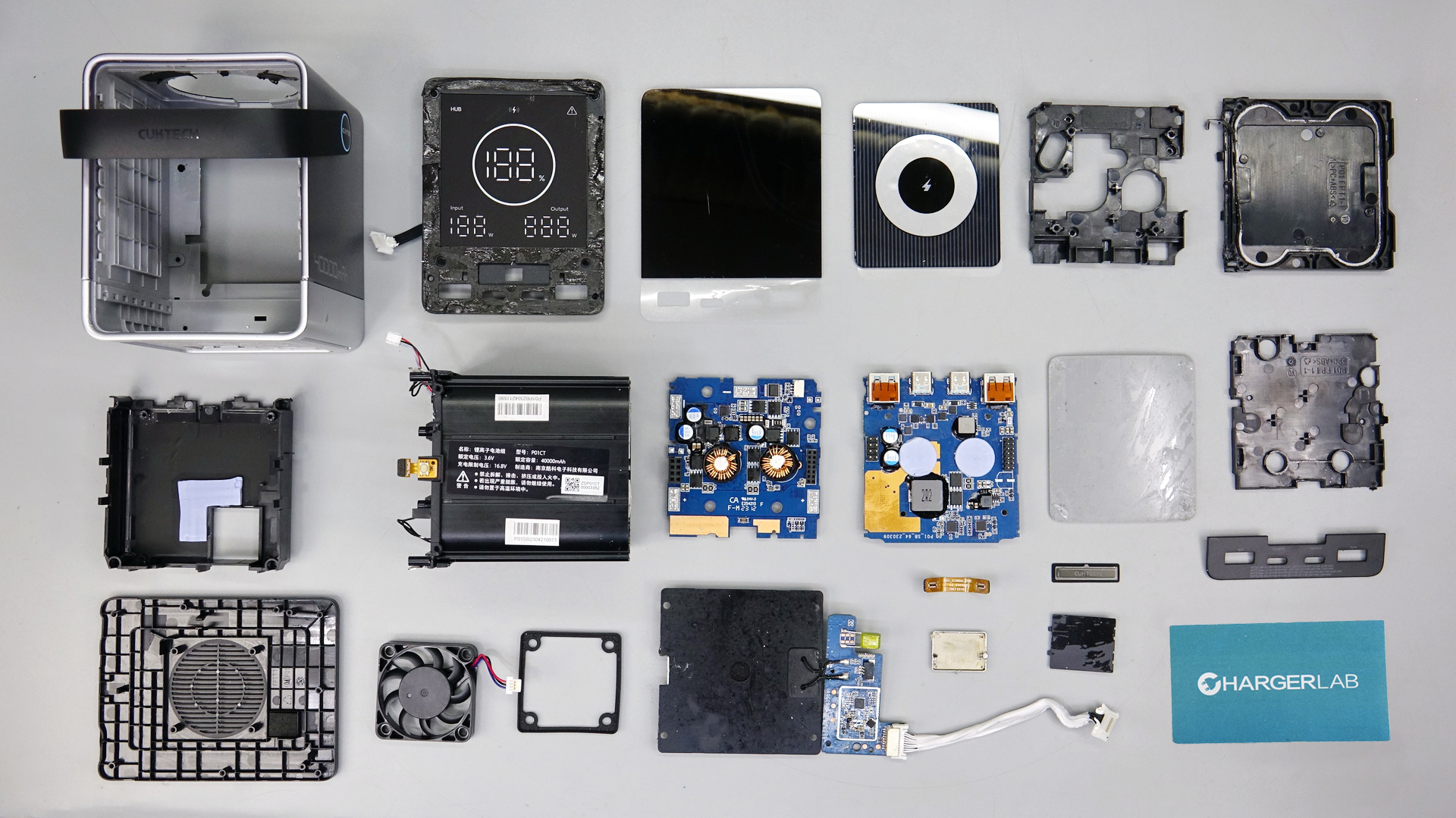
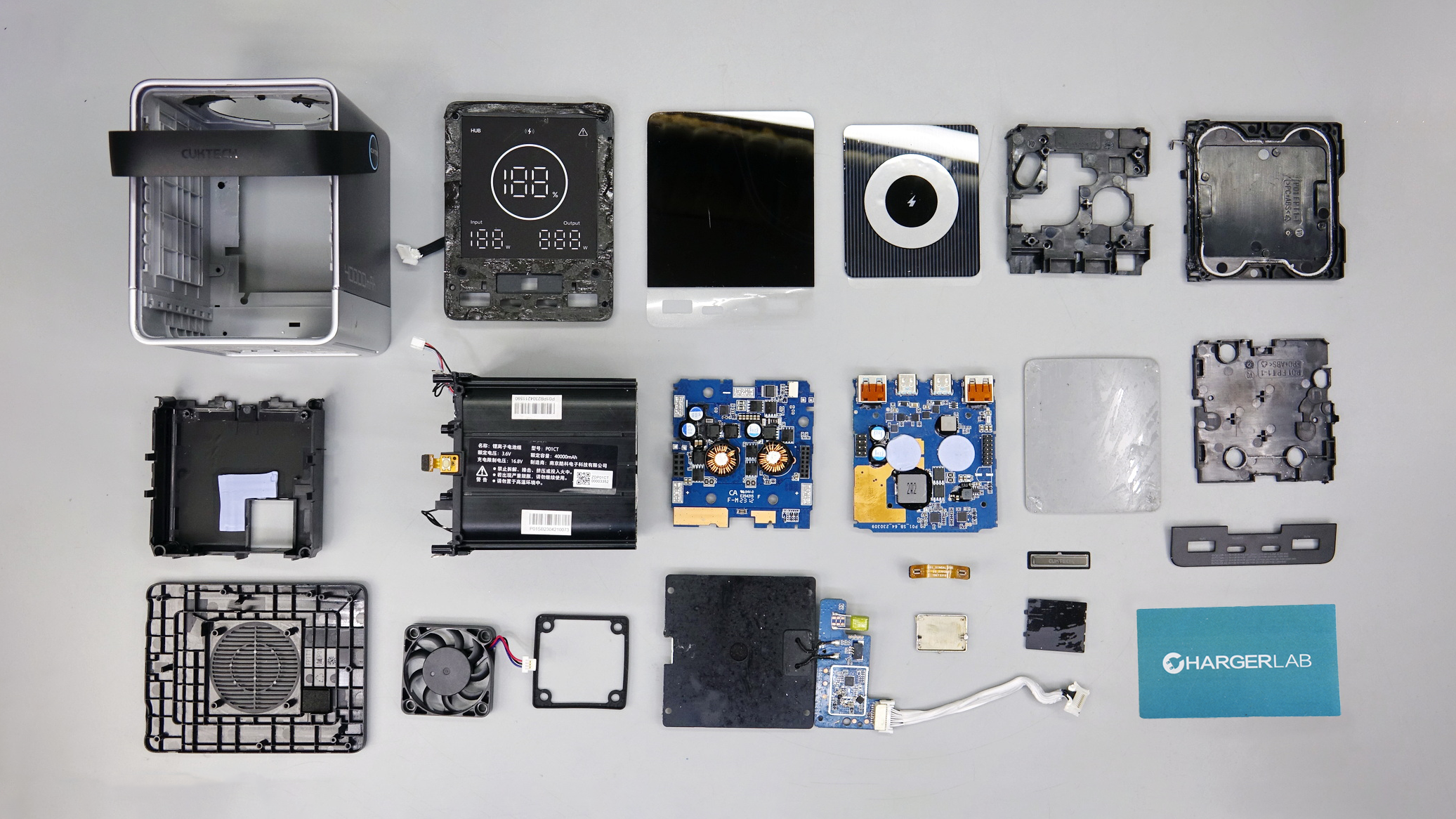
Well, that's all components of this CUKTECH No.30 PD3.1 & 300W Power Bank.
Summary of ChargerLAB
Well, as the world's smallest 300W power bank, this device can be seen as a miniature version of a portable power station, offering impressive power capacity in a compact size. It is particularly suitable for Apple laptop users, Xiaomi smartphone users, DIY enthusiasts, as well as people who prioritize portability without the need for AC power while on the go.
After taking it apart, we found it consists of eight battery cells, two stacked output PCBs, wireless charging module, and a cooling fan. The compact and robust internal structure ensures efficient and reliable performance. With the top handle, this power bank allows you to easily carry it wherever you desire. However, it is important to note that due to aviation regulations, this power bank cannot be taken on a plane.
Related Articles:
1. CUKTECH Launched No. 30 Power Bank at Hong Kong Electronics Show
2. Experience Next-Level Fast Charging with the CUKTECH P Series 210W Power Bank
3. Teardown of CUKTECH No.30 PD3.1 & 300W Power Bank (Video)

