You can support them on Indiegogo: https://igg.me/at/cuktech/x#/
If you wanna buy the tester of POWER-Z, you can visit our Amazon store: Click here.
Introduction
---------------------------------------------------------------
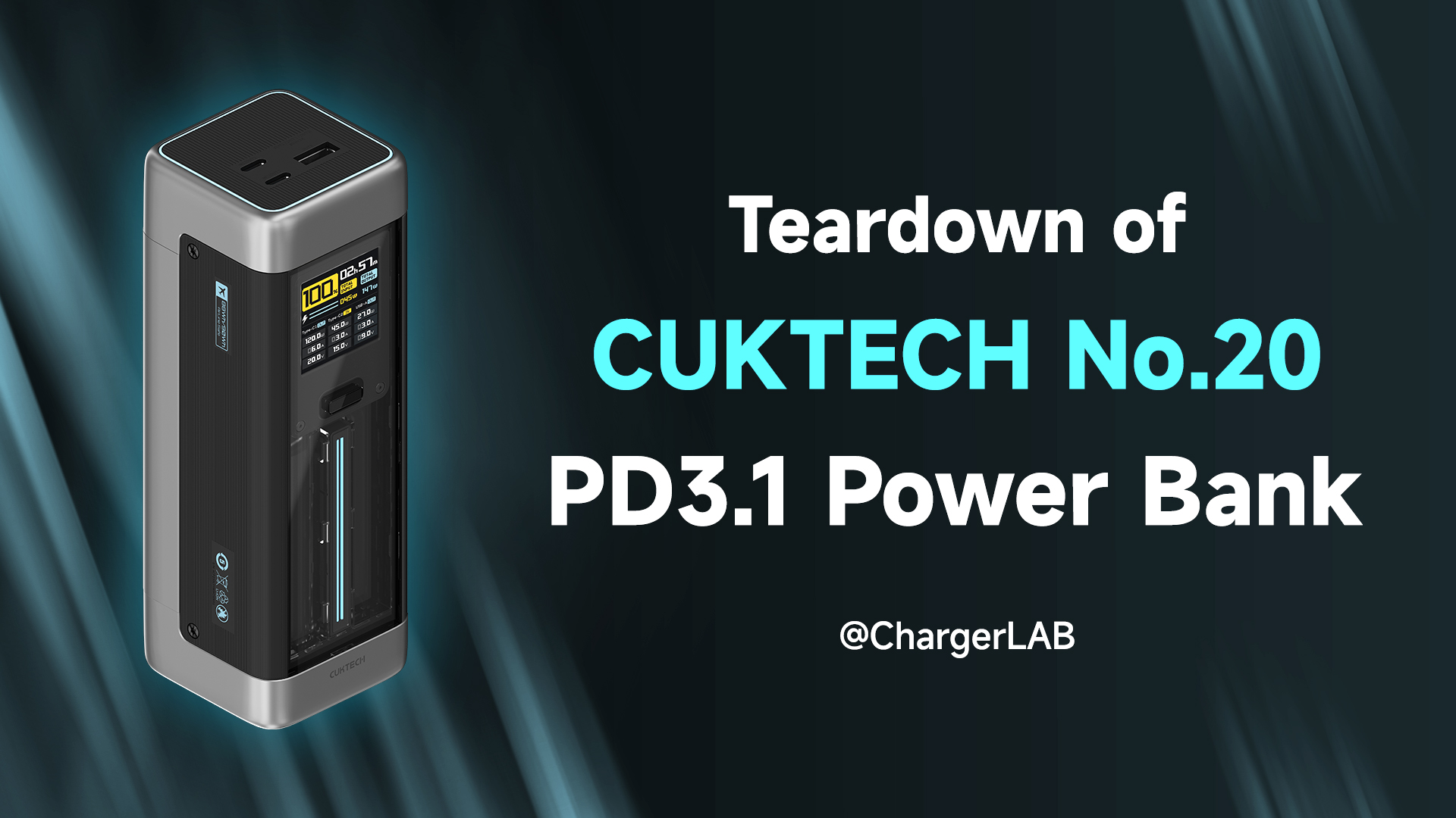
Several weeks ago, we posted a teardown video of the CUKTECH No.30 power bank. And today, we got another power bank from CUKTECH, the No.20 power bank. It looks like the Anker 140W PD3.1 power bank we took apart before. Let's go ahead and take apart this power bank to see what it looks like inside.
Bill of materials (BOM)
------------------------------------------
Battery Cell: EVE
MCU: WCH CH32V303RCT6
Buck-boost Controller (USB-C2): Southchip SC8815
Synchronous Buck-boost MOSFET (USB-C2): AOS AON6354
Solid Capacitor: CapXon
VBUS MOSFET (USB-C2): TPCC8104
Buck-boost Controller (USB-C1): Southchip SC8815
Synchronous Buck-boost MOSFET (USB-C1): AOS AONS66406
Synchronous Buck-boost MOSFET (USB-A): Southchip SC8721
Protocol Chip: ABOV A94P829
Battery Protection Chip: iCM CM1351
Battery Protection MOSFET: AOS AON6512
Related Articles:
1. Experience Next-Level Fast Charging with the CUKTECH P Series 210W Power Bank
2. Teardown of CUKTECH No.30 PD3.1 & 300W Power Bank
3. CUKTECH Launched No. 30 Power Bank at Hong Kong Electronics Show


