Introduction
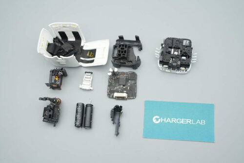
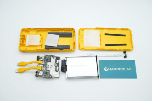
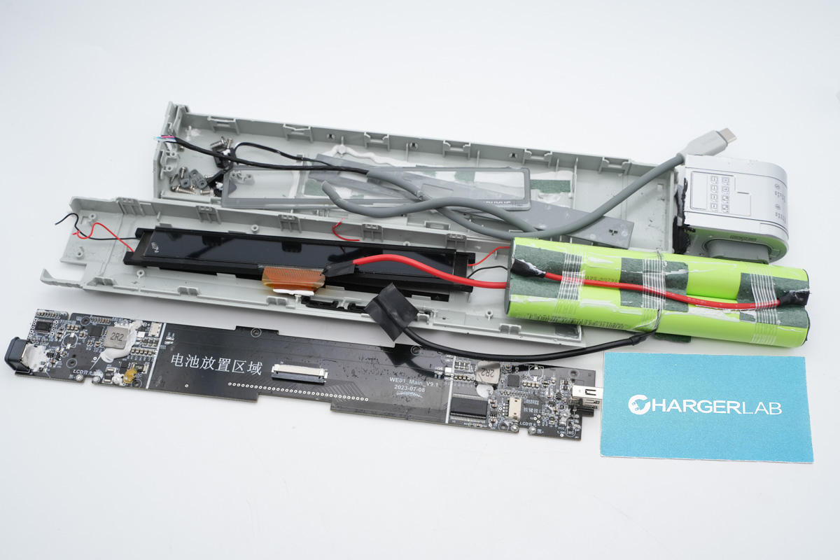
CUKTECH is one of the rising stars of high-performance power banks and chargers. We've taken apart its No.20 and No.30 power bank. Both models can support PD3.1, but may be a bit pricey for some people.
Today we’re going to take apart a more affordable option, the No.15 power bank.
Product Appearance
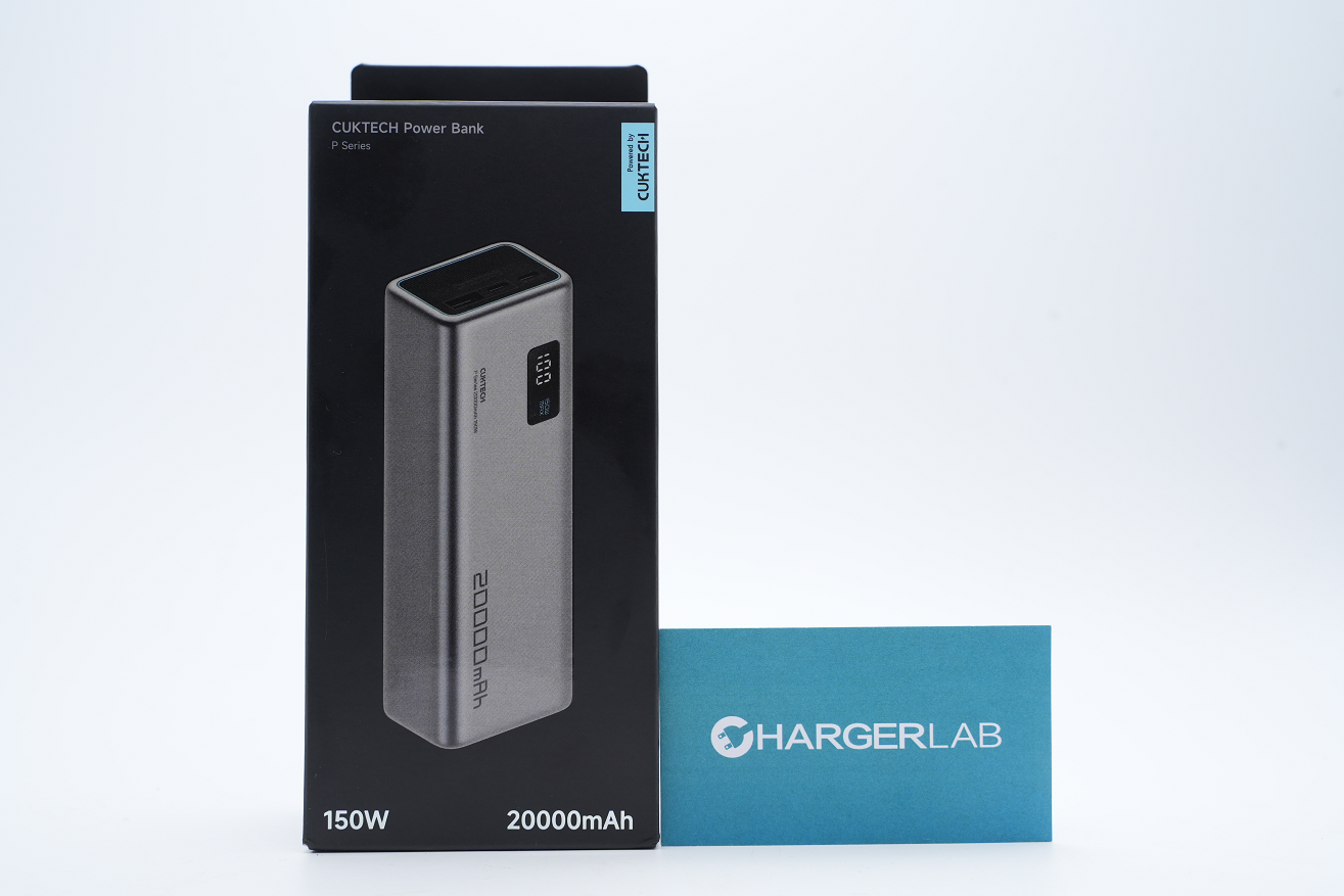
As you can see, it can do 150W.
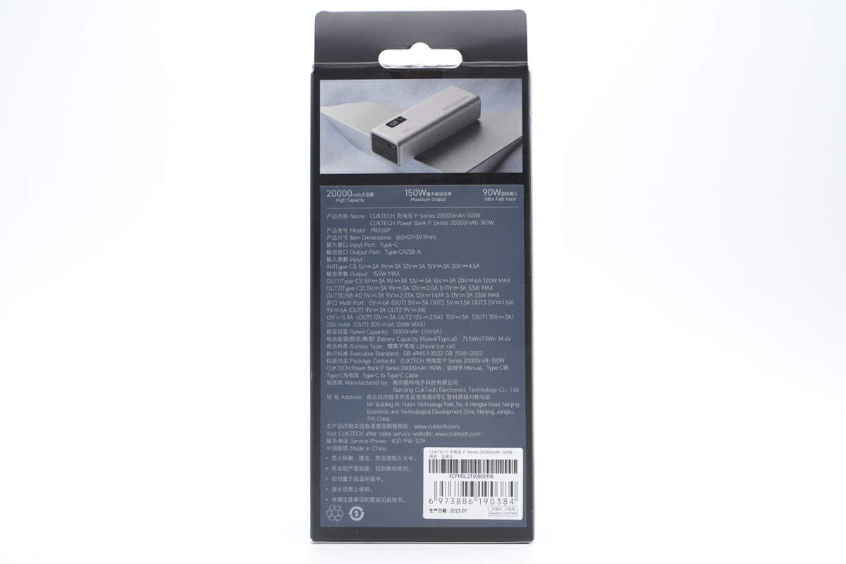
Flip to the back.
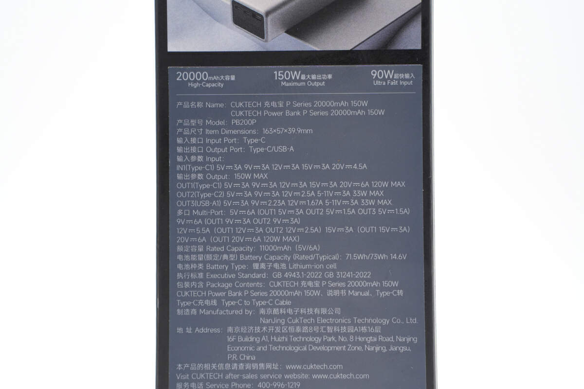
All specs info are here. We'll talk about it later.
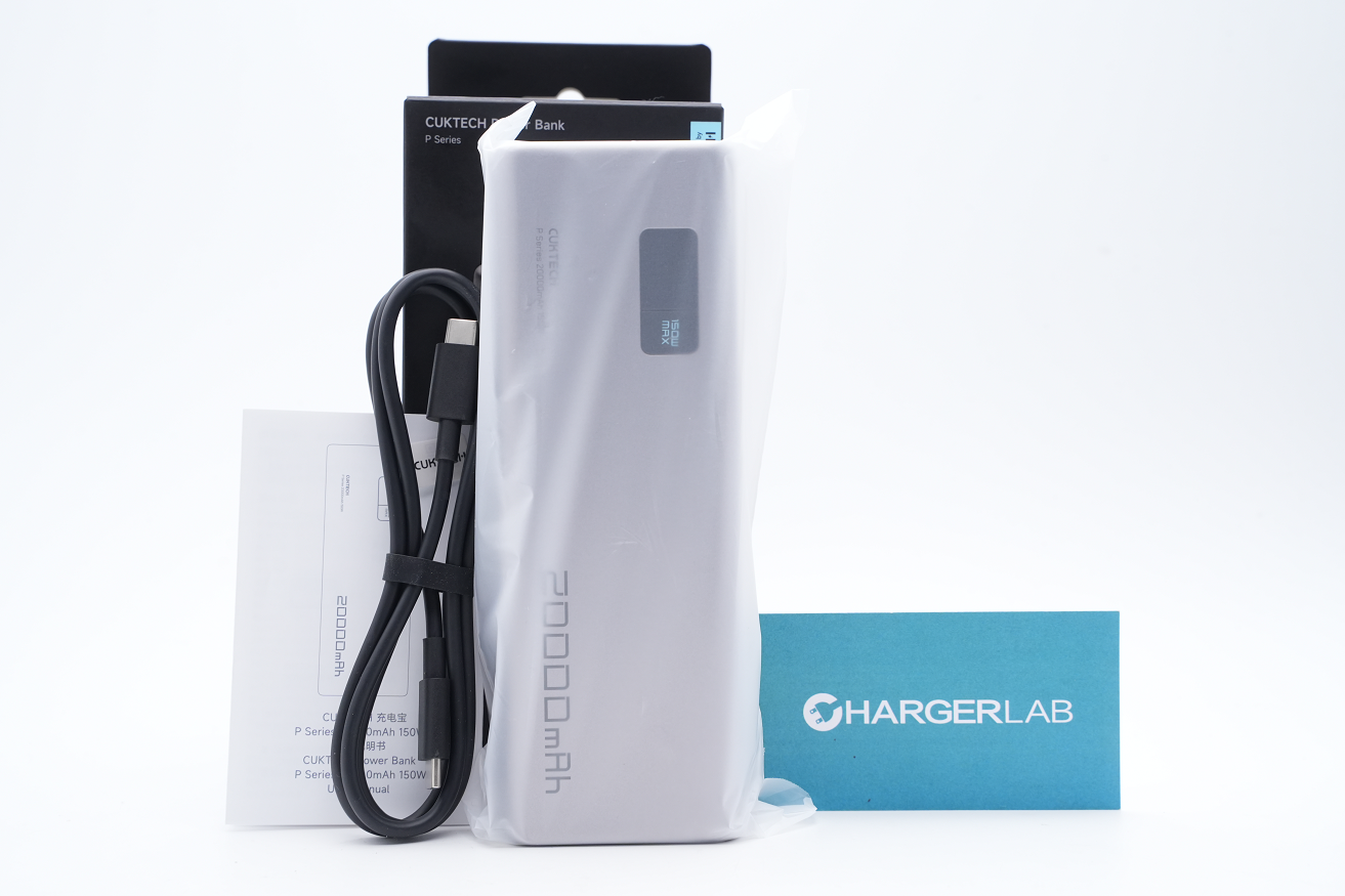
Open the box. And take out the power bank.
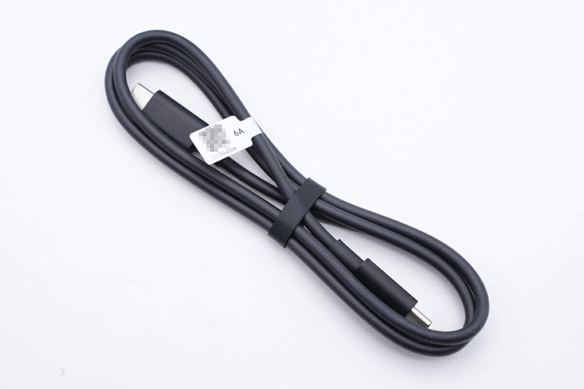
It also comes with a dual USB-C cable, with a 6A label on it.
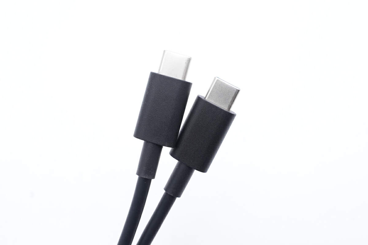
The connector is designed with matte.
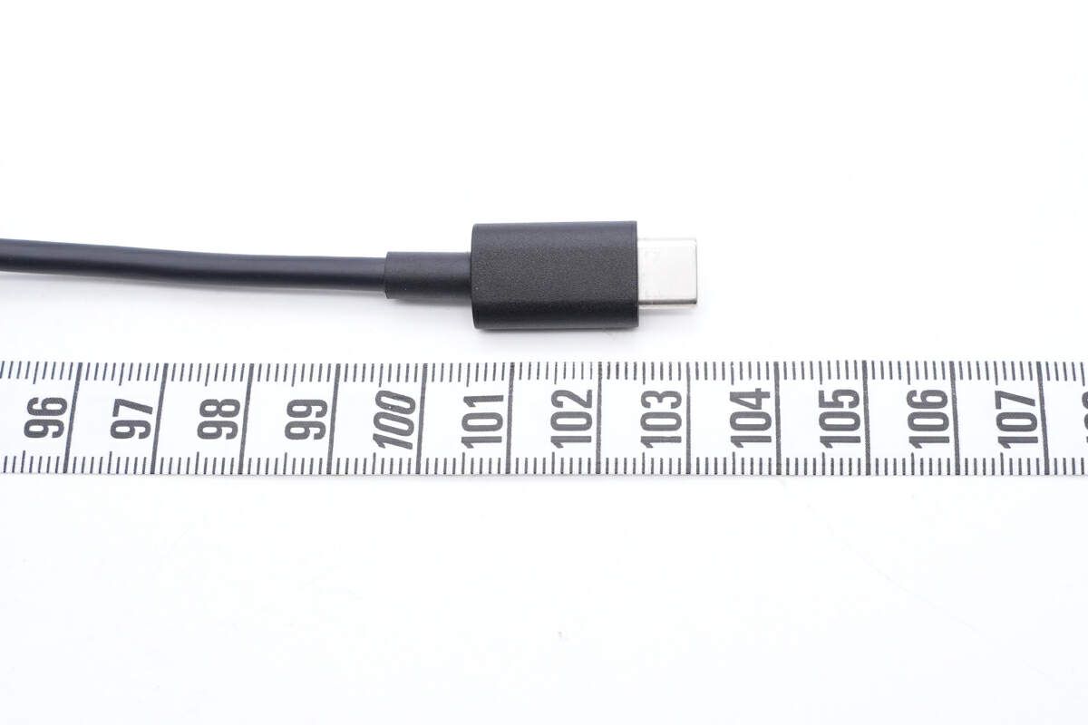
The length of the cable is about 1M (3' 3.37'').
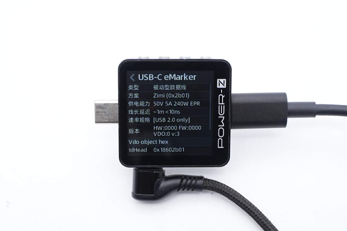
The ChargerLAB POWER-Z KM003C shows it supports USB PD3.1. And the charging speed can be up to 240W.
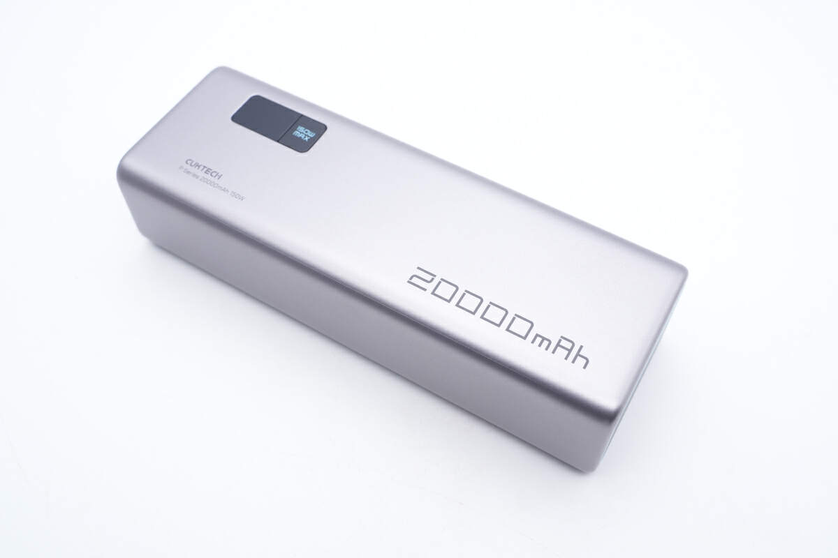
It still features a long, rectangular design, with a PC fireproof shell, giving it an overall aesthetic appeal.
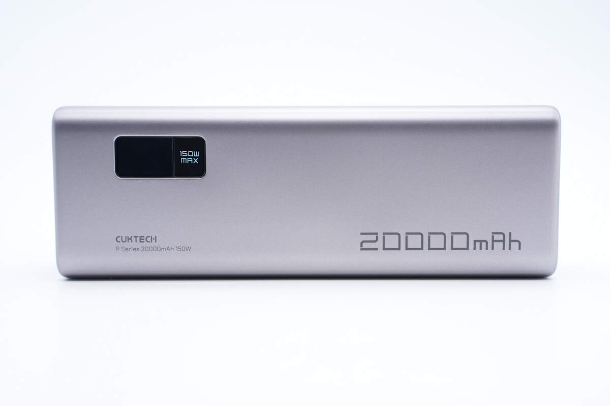
There's a small display in the upper left corner, which indicates the remaining battery. And the 150W MAX design on the power button highlights the most critical feature.
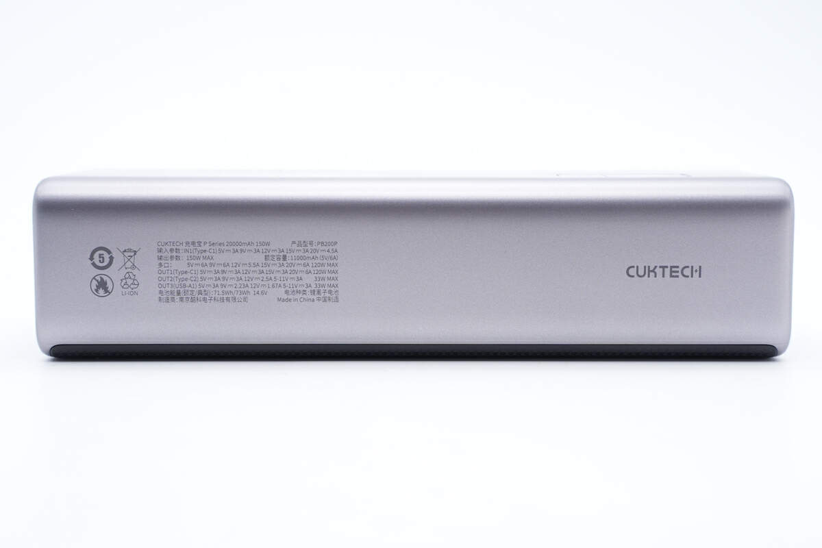
Then, let me introduce the detailed specs info.
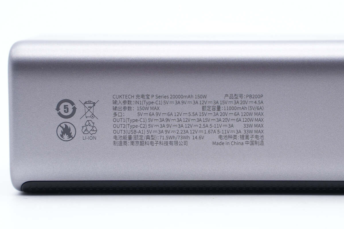
Model is PB200P. The battery capacity is 20000mAh. And the energy is about 73Wh. The USB-C1 can support up to 90W input power. And it can output up to 120W when using a dedicated 6A cable and supported devices.
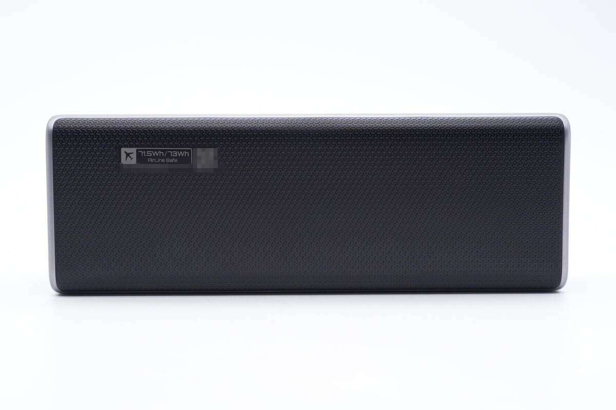
On the back, it features a unique textured design.
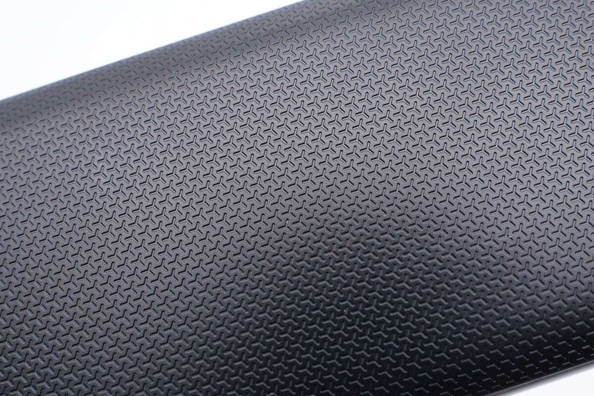
These small "Y" bumps and grooves on the rubber pad at the bottom can increase the friction. So, you can hold it more tightly.
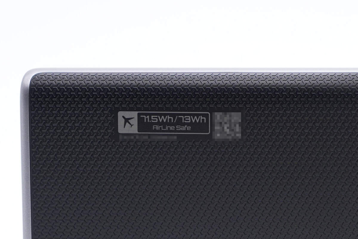
Since the maximum energy does not exceed 100Wh, there is no problem taking it with you on the plane in most countries and regions.
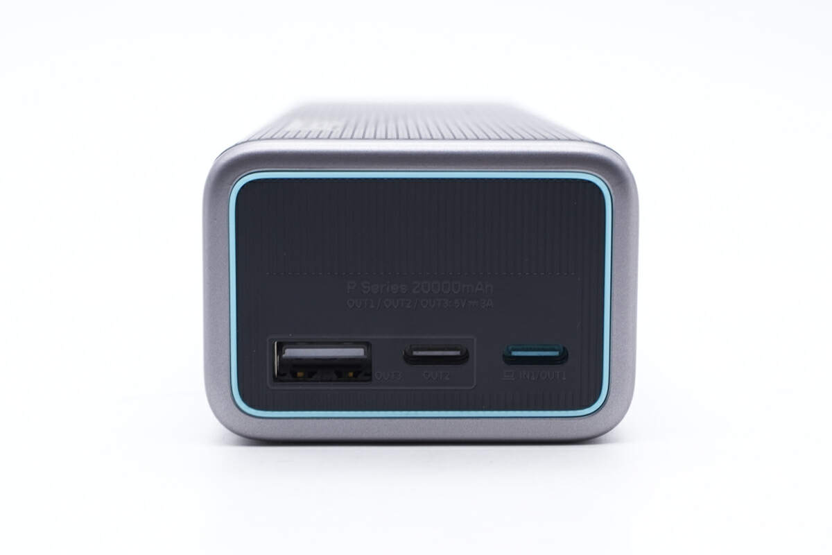
The output panel is on the top. There are two USB-C and a USB-A port. Only the USB-C1 supports input and output at the same time.
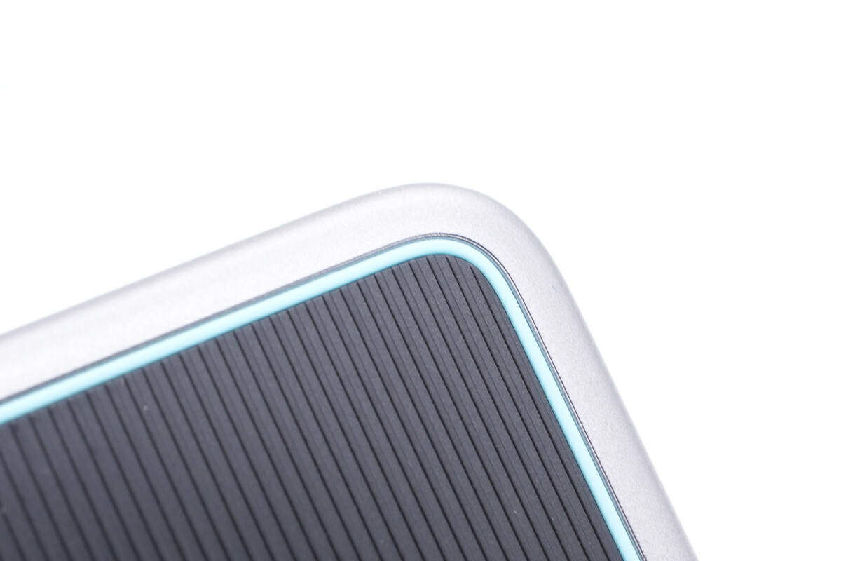
This striped texture is identical to what we've encountered before when we took apart the No. 20.
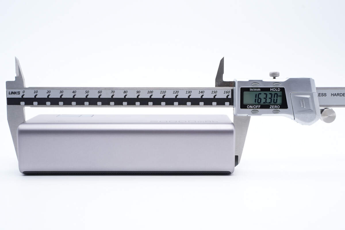
The length of the power bank is about 163mm (6.42 inches).
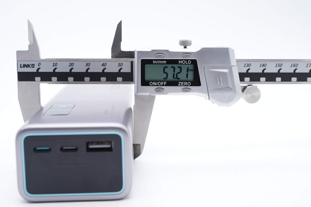
The width is about 57mm (2.24 inches).
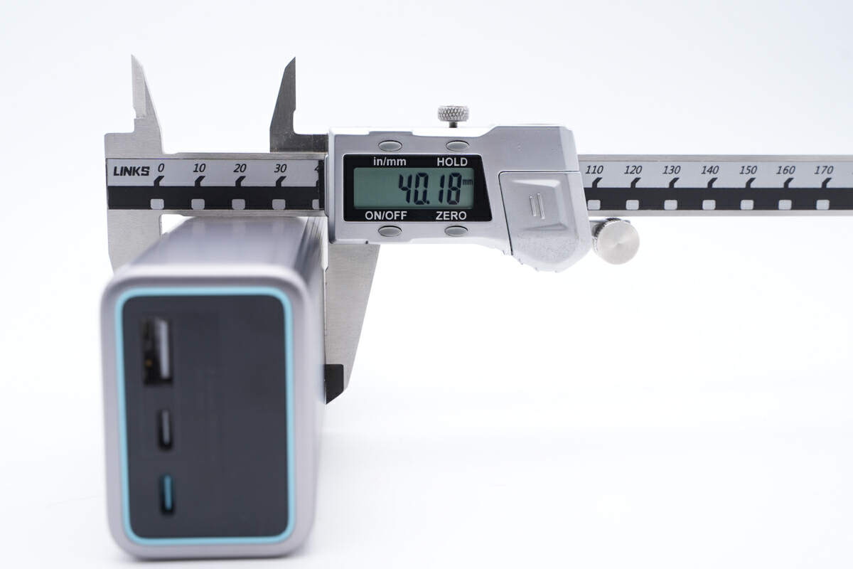
And the height is about 40mm (1.57 inches).
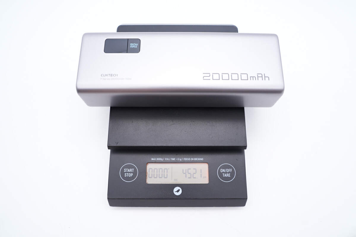
And the weight is about 452g (15.94 oz).
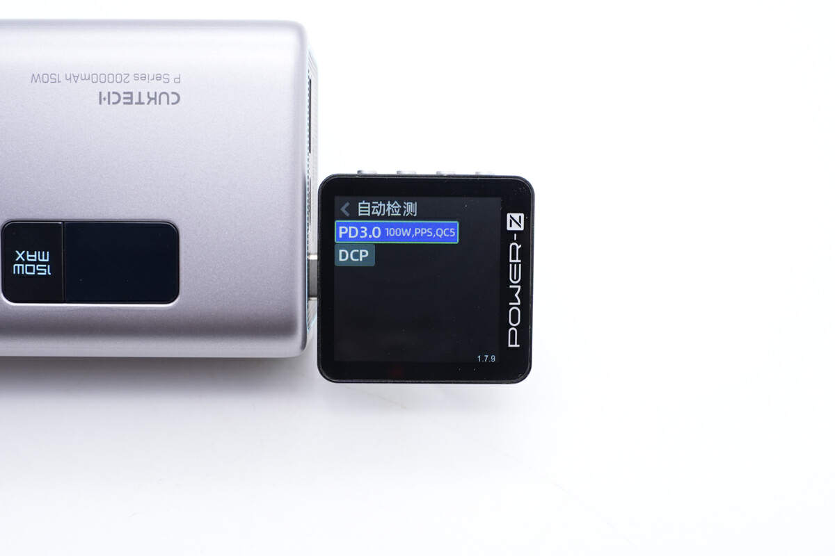
The ChargerLAB POWER-Z KM003C shows the USB-C1 supports PD3.0, PPS, QC5, and DCP protocols.
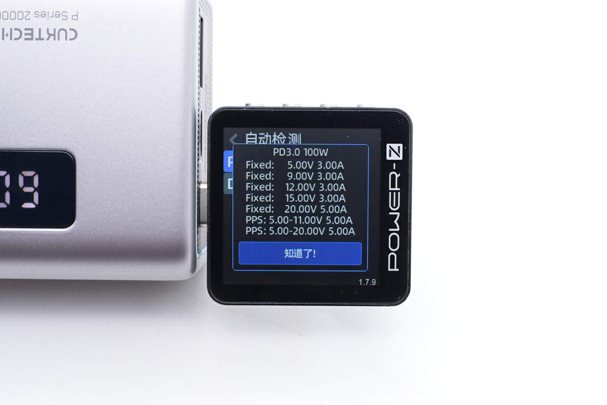
It has five fixed PDOs of 5V/ 9V/12V/15V3A, 20V5A, and two sets of PPS.
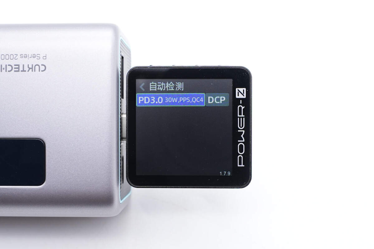
The USB-C2 also supports PD3.0, PPS, QC4, and DCP protocols, but the power drops from 100W to 30W.
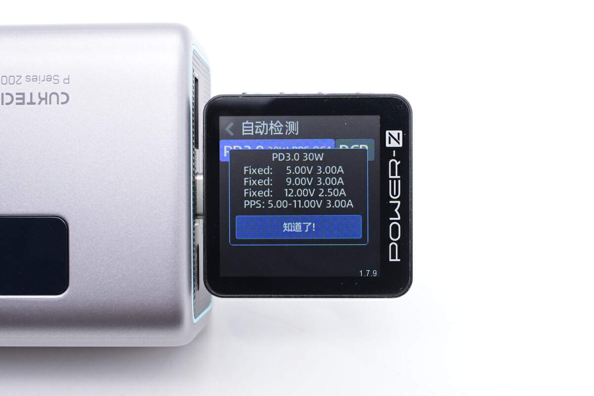
It also has three fixed PDOs of 5V/9V3A, 12V2.5A, and a set of PPS.
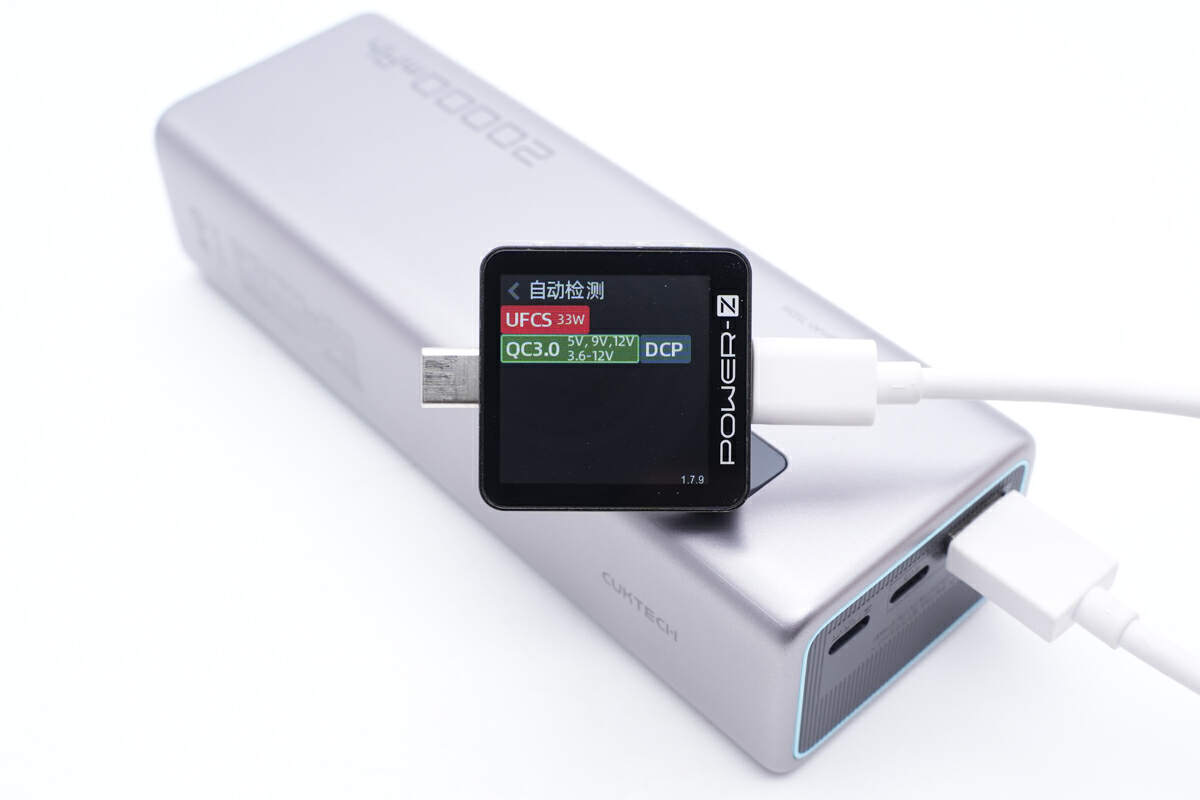
Finally, the USB-A supports UFCS, QC3.0, and DCP protocols.
Teardown
Now that we have completed our testing of this power bank, it's time to take it apart and examine its internal components and structure.
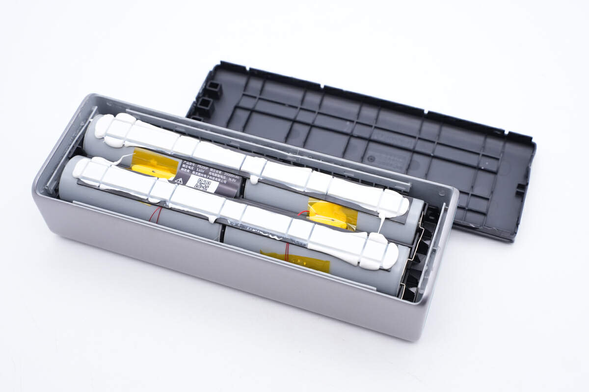
Firstly, pry along the gap to remove the rubber pad at the bottom. As we can see, there are some silicone adhesives pasted on the battery cells.
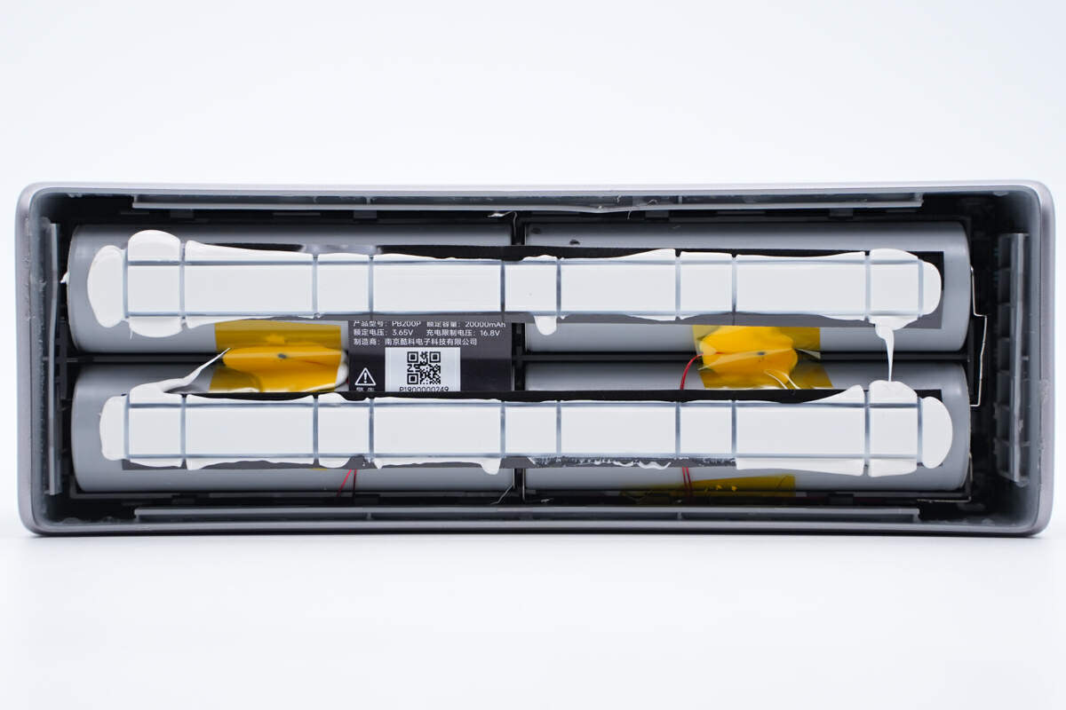
Four battery cells are connected in series. Two thermistors are pasted under the heat-resistant tape for temperature detection.
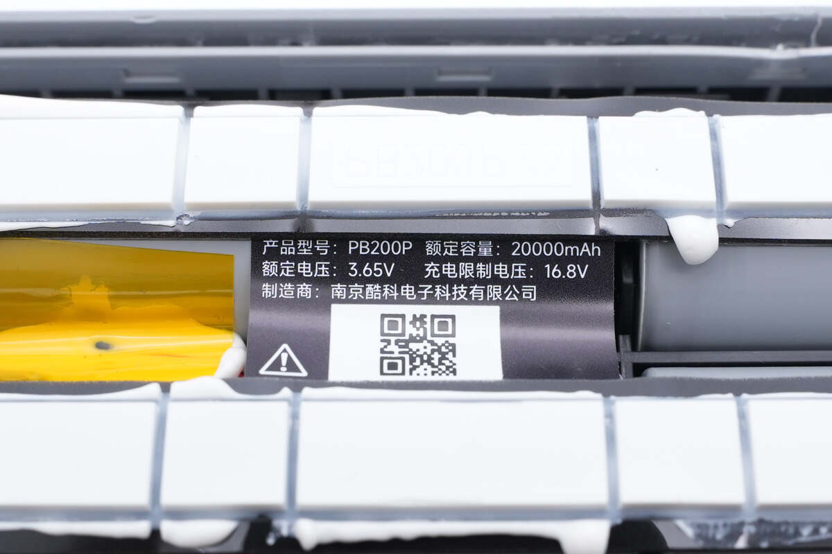
And the total capacity is 20000mAh, so it's 5000mAh for a single battery cell.
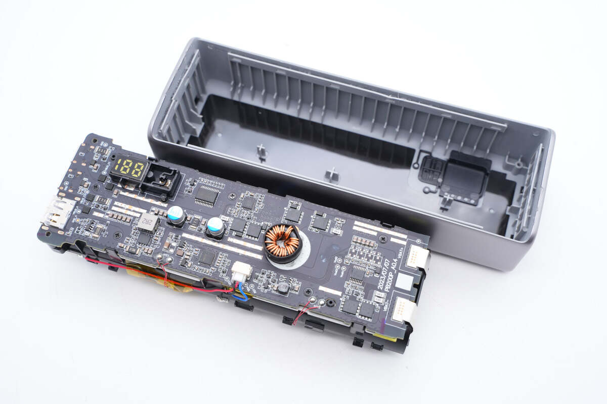
Continue to remove fixing screws. And separate the internal module.
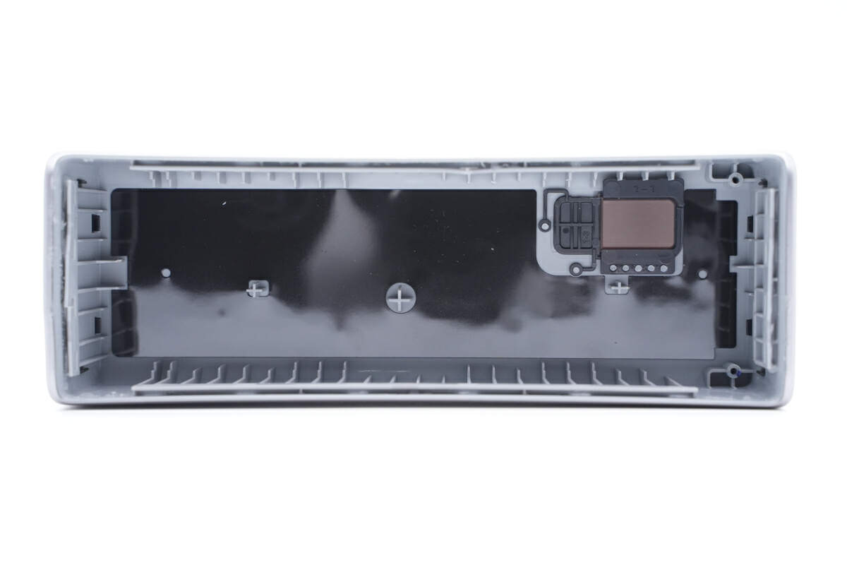
The PCB is covered with a layer of black shielding.
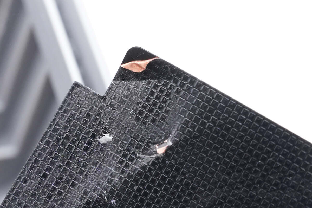
It's actually the copper foil thermal material.
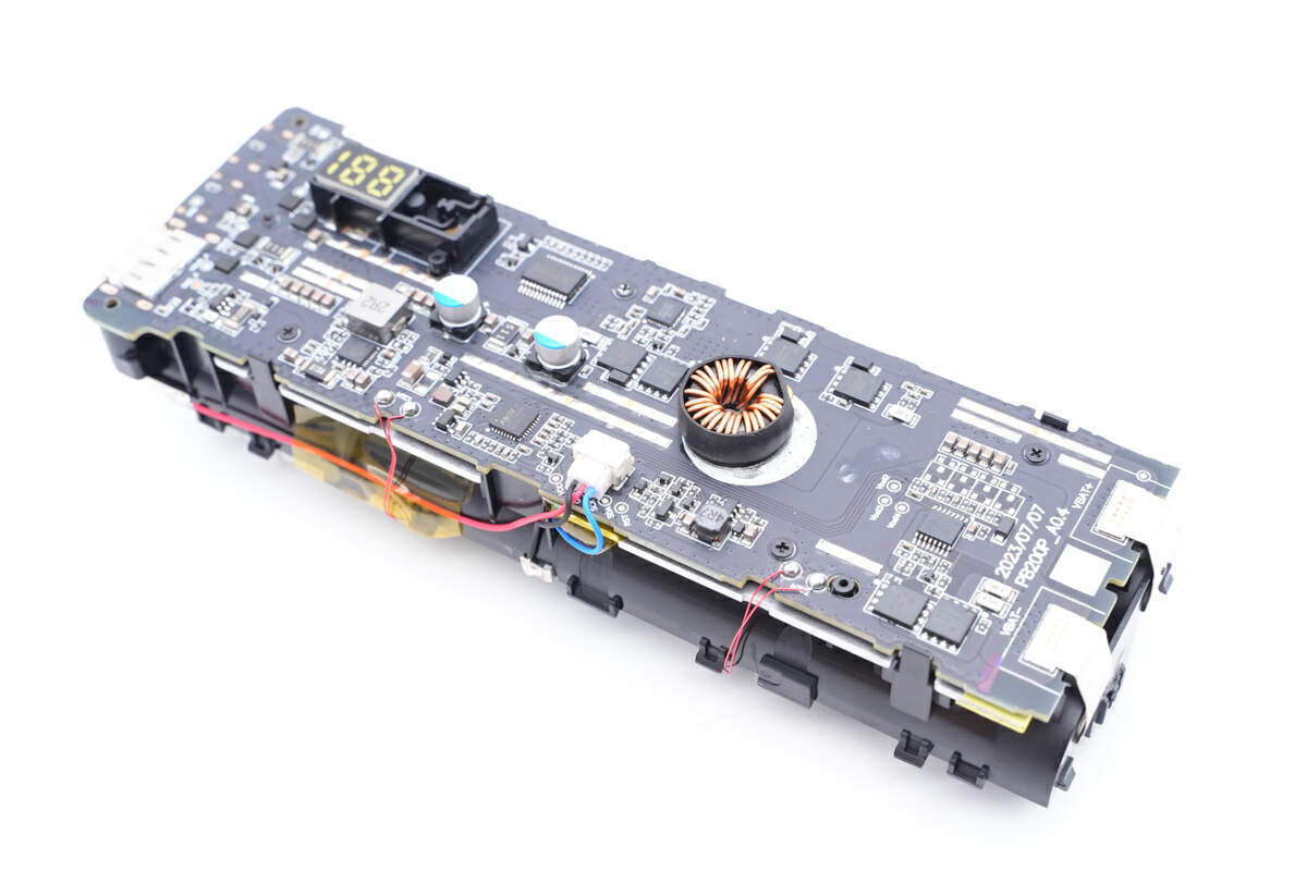
The main PCB is on the other side of the power bank. The blue, red, and black wires for voltage sampling are used to detect three different places of four battery cells.
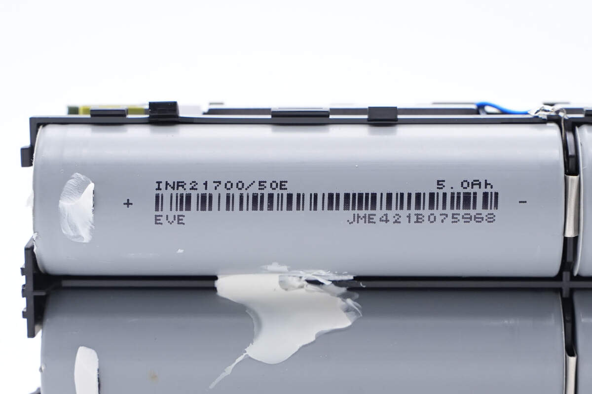
Take a closer look at the 21700 battery cells. They're from EVE. And the capacity is 5 Ah for each one.
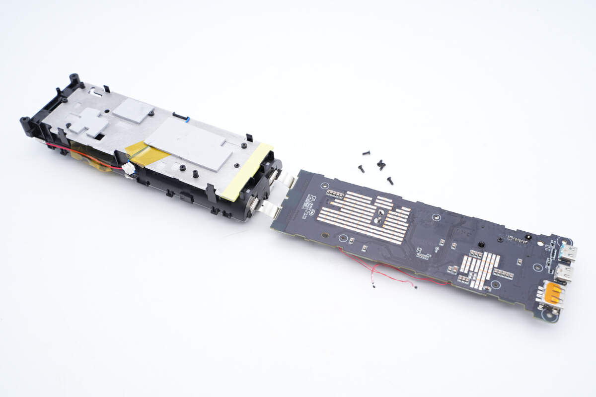
Then, let's remove all fixing screws. And separate battery cells and PCB.
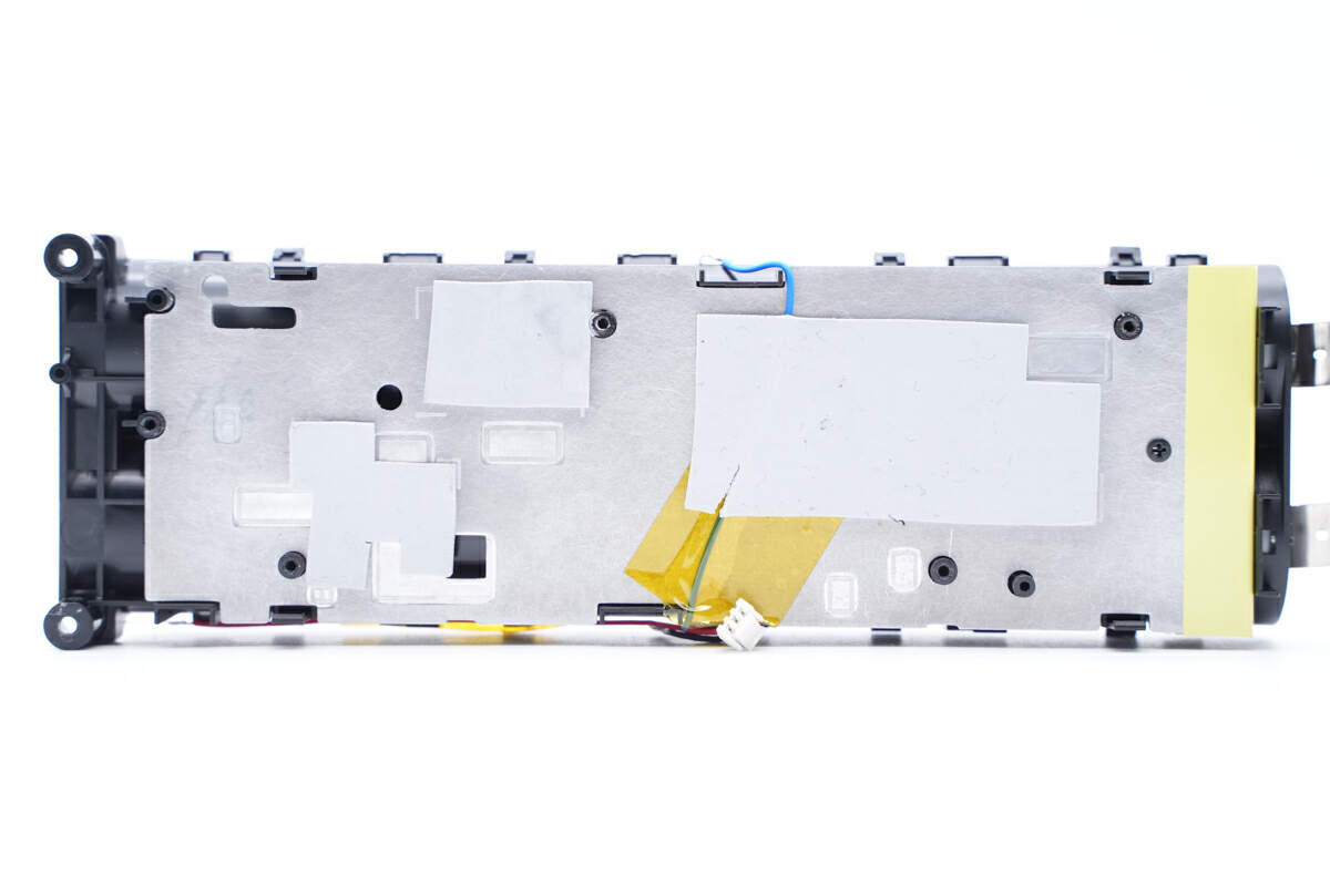
The main PCB is placed on an aluminum plate and fixed with a plastic frame.
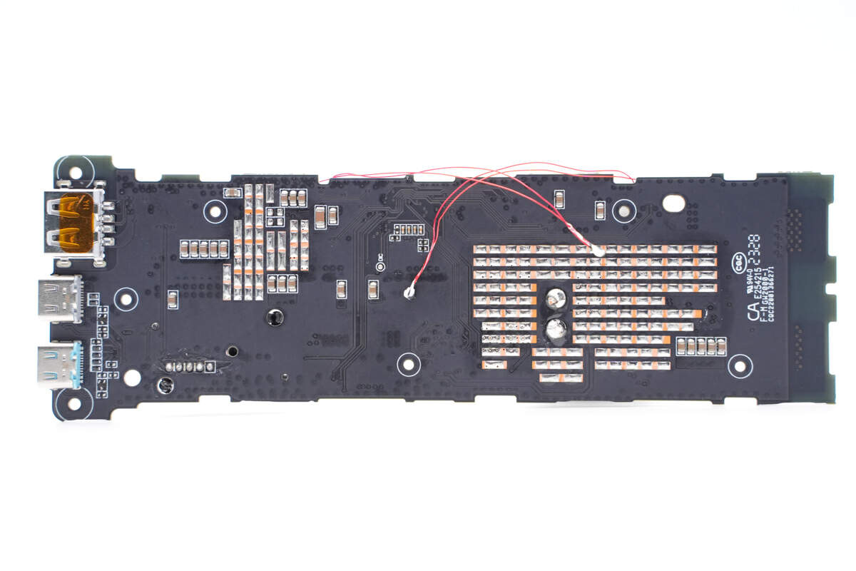
Those thermal pads on the aluminum plate and exposed copper on the back of the PCB can greatly enhance its heat dissipation performance.
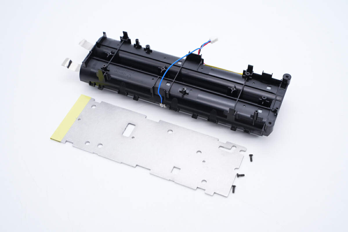
Remove the aluminum plate too.
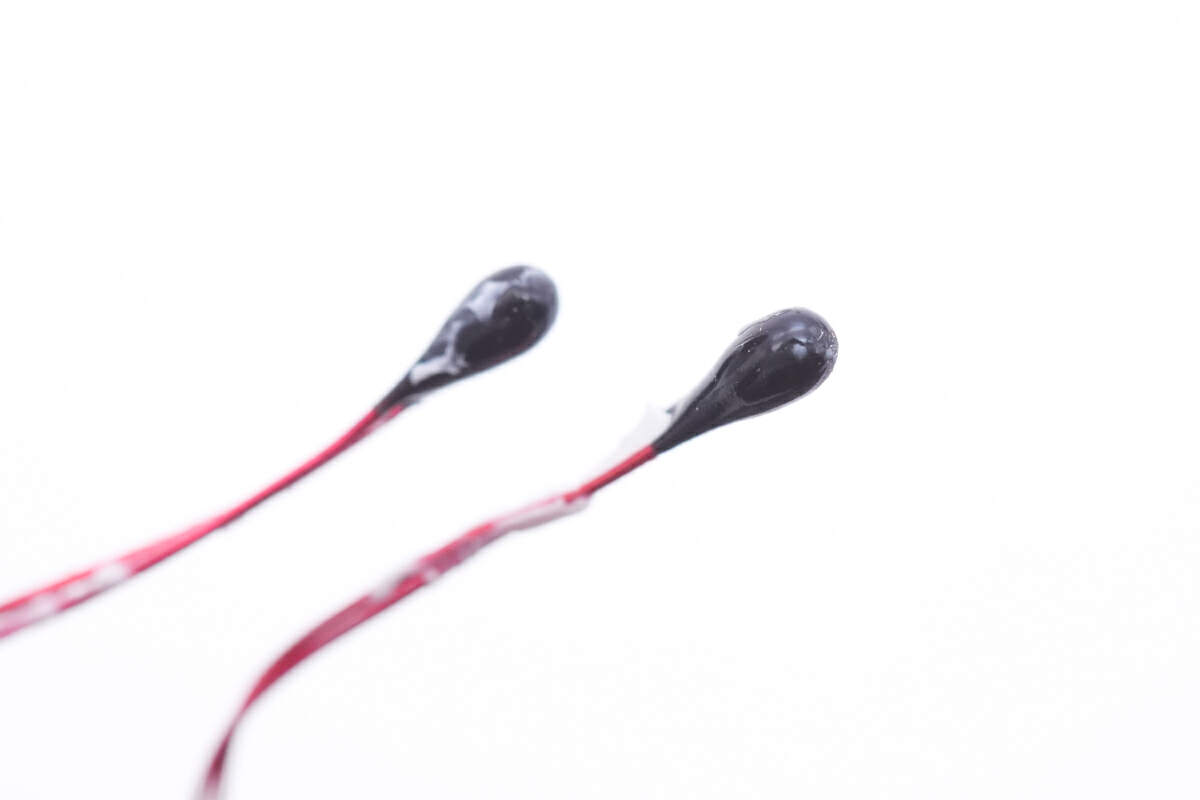
The two thermistors mentioned above are used to detect battery temperature.
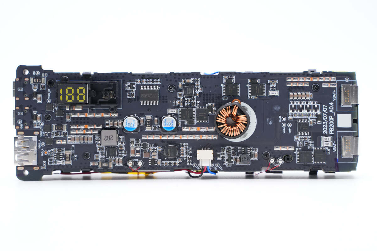
The synchronous buck-boost converter, alloy inductor, magnetic ring inductor and battery protection chip are on the front of the PCBA module. Almost all components are on the front of the PCB. Let's introduce them one by one.
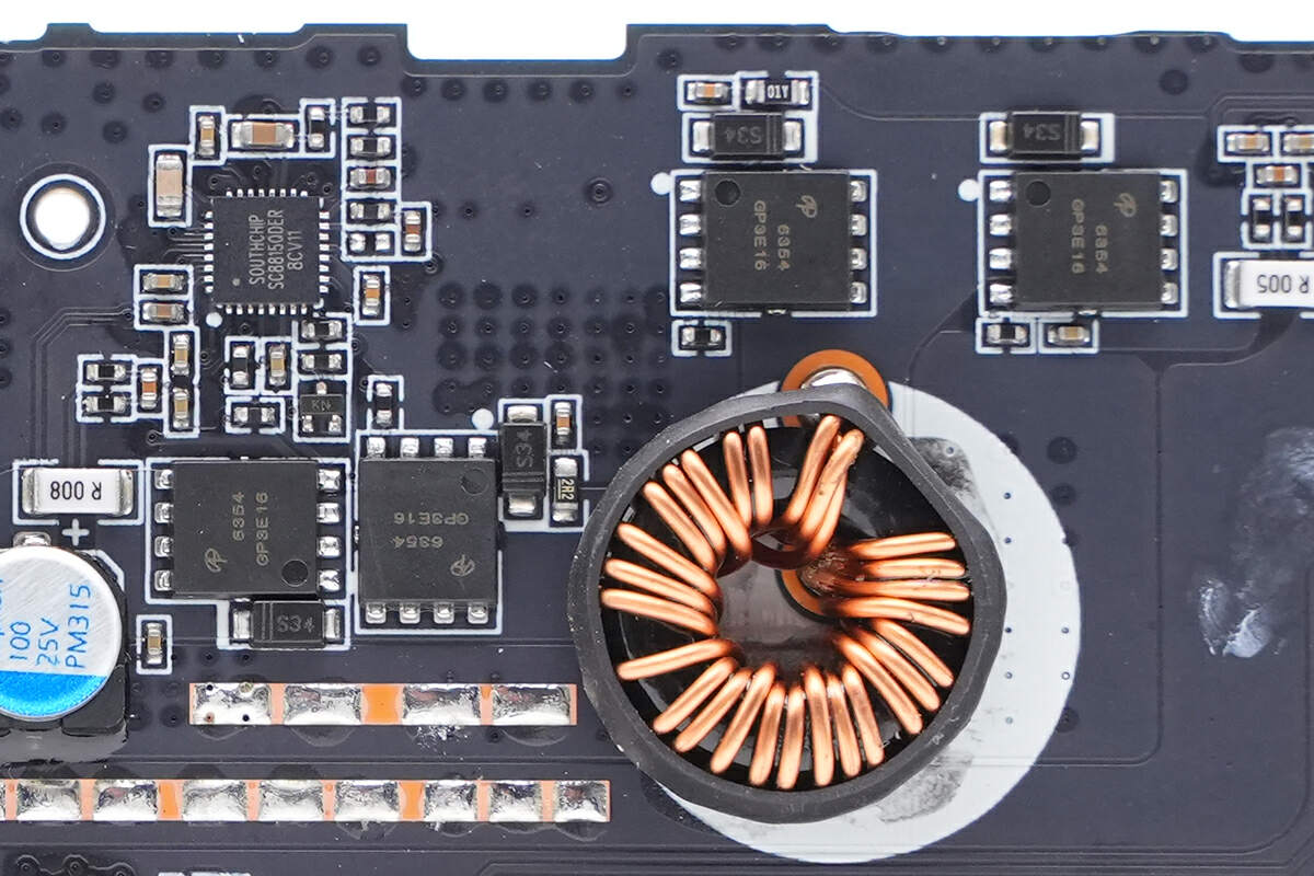
Start from the circuit of USB-C1.
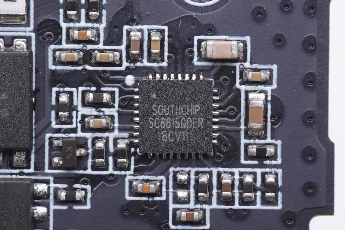
The buck-boost controller of USB-C1 is from Southchip and is used to control DC input and USB-C output. It integrates the I²C protocol, which can control current limits, reverse discharge, etc. Model is SC8815.
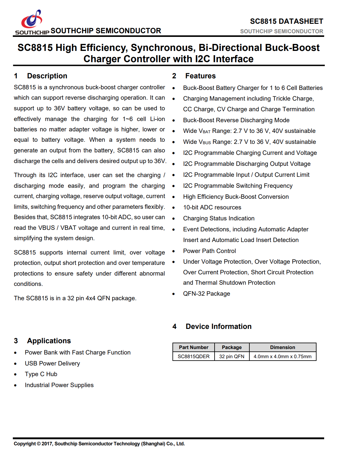
Here is all the information about the Southchip SC8815.
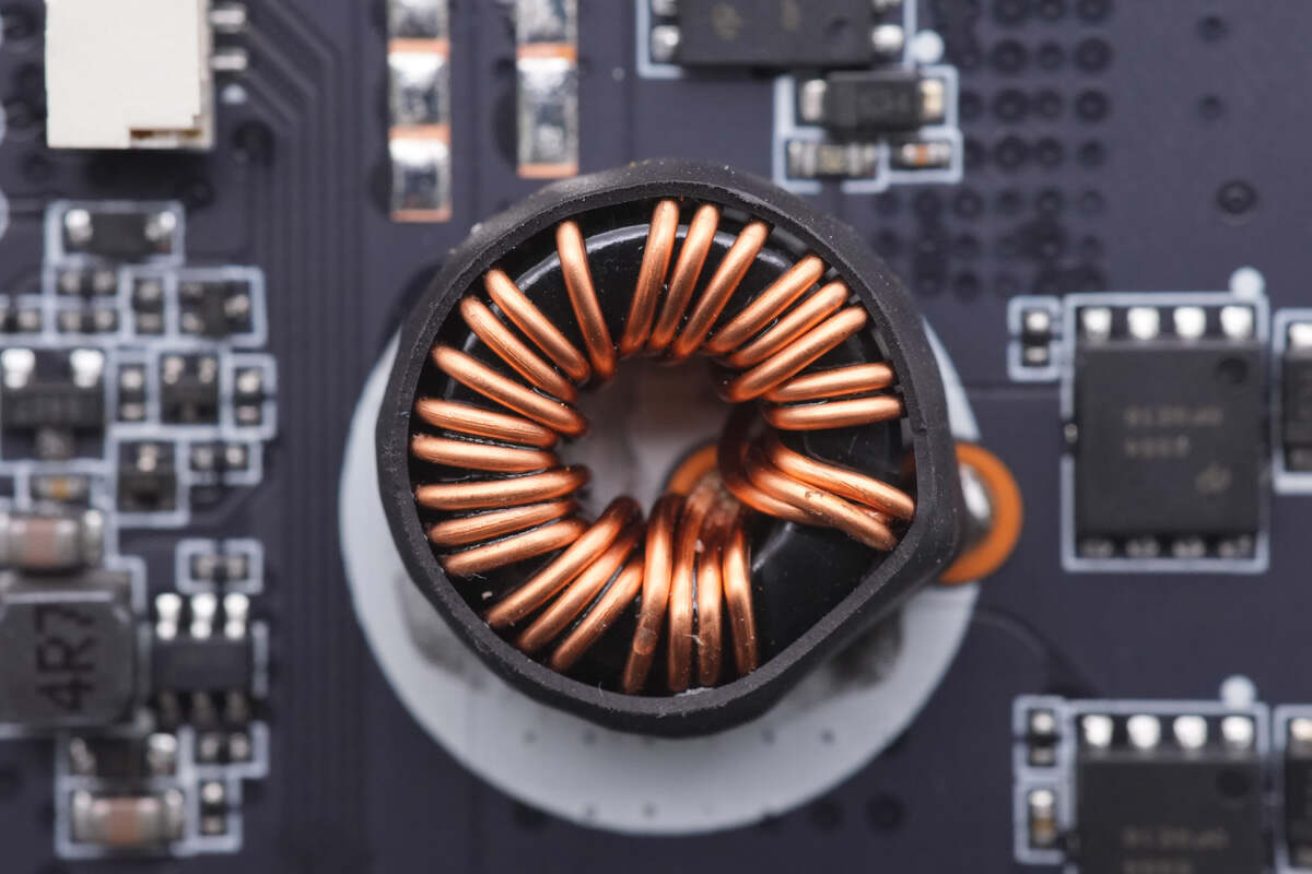
The largest buck-boost inductor is wound with three wires in parallel and is insulated with heat-shrinkable tubing.
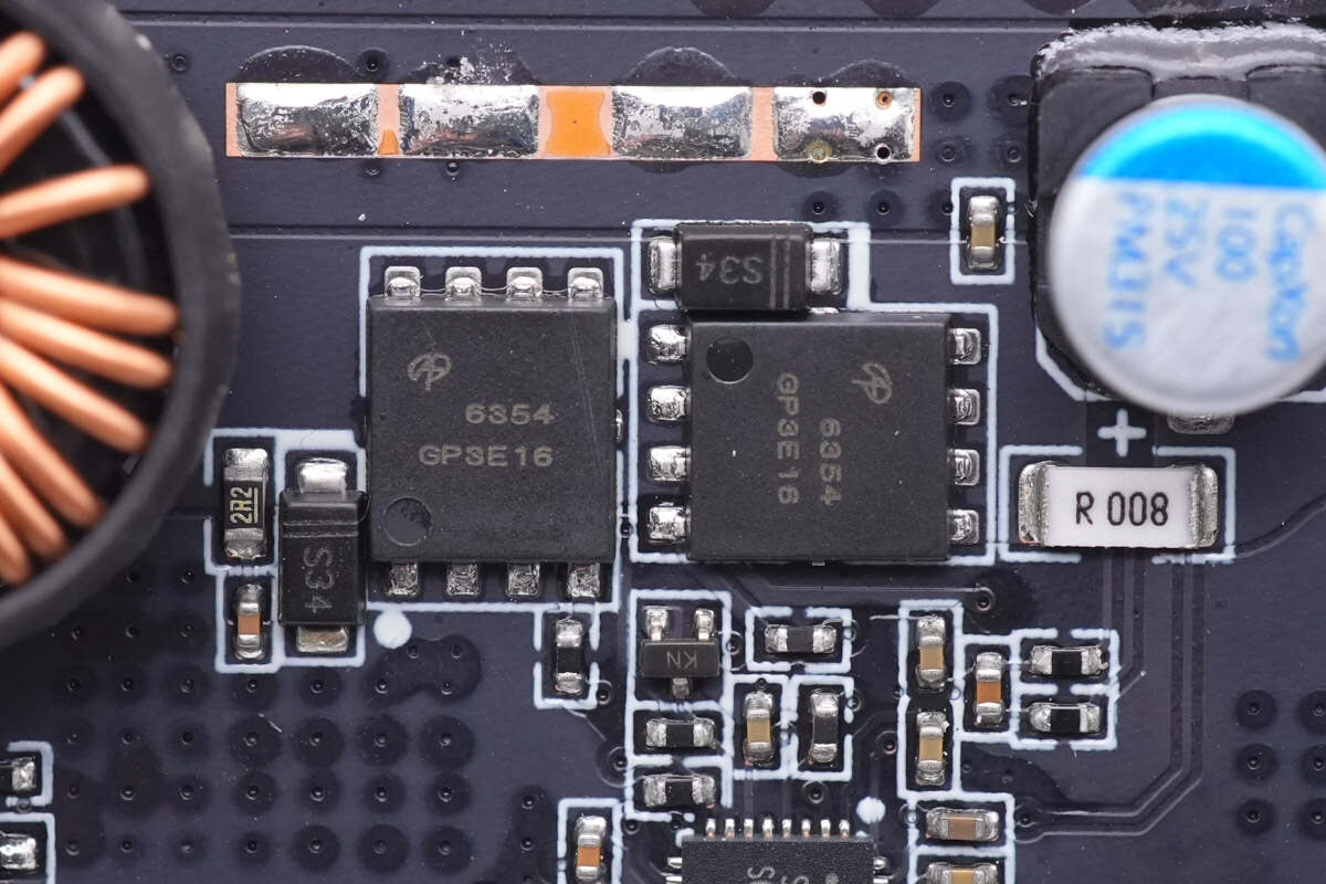
Those two synchronous buck-boost MOSFETs of the USB-C1 are from AOS and adopt DFN5 x 6 package.
30V, 2.75mΩ. Model is AON6354.
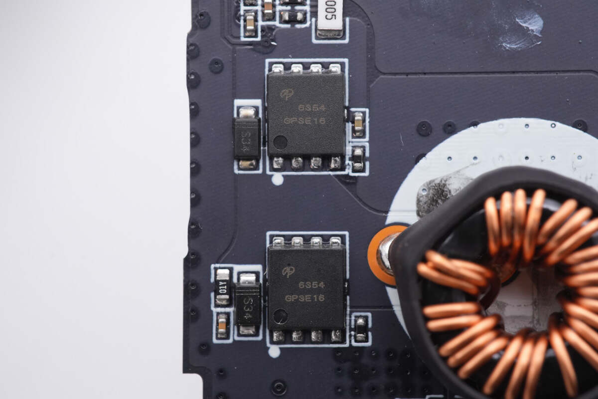
Here are the other two AON6354.
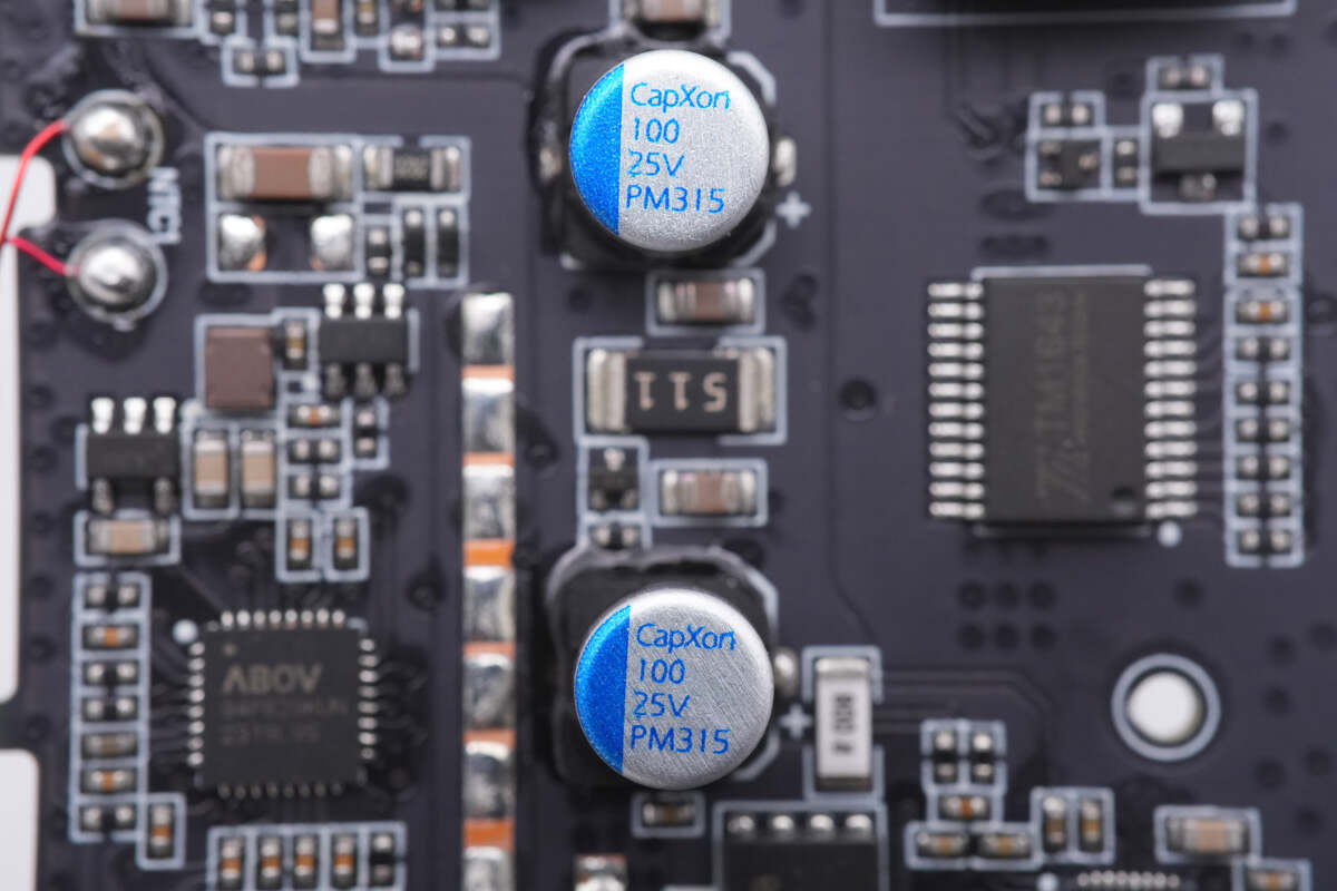
Two blue solid capacitors for output filtering of USB-C1 are from CapXon PM series. They're connected in parallel and fixed with glue. 100μF 25V for each one.
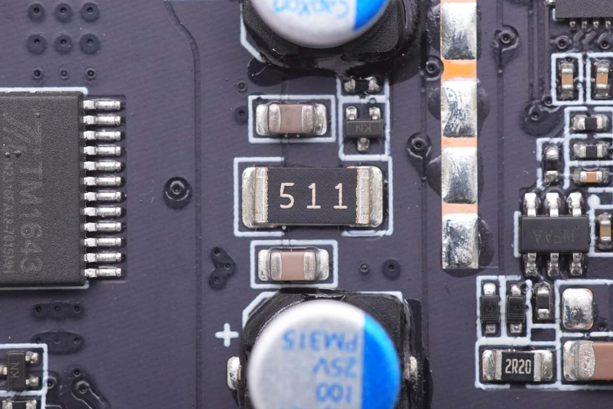
A discharge resistor is soldered between two capacitors.
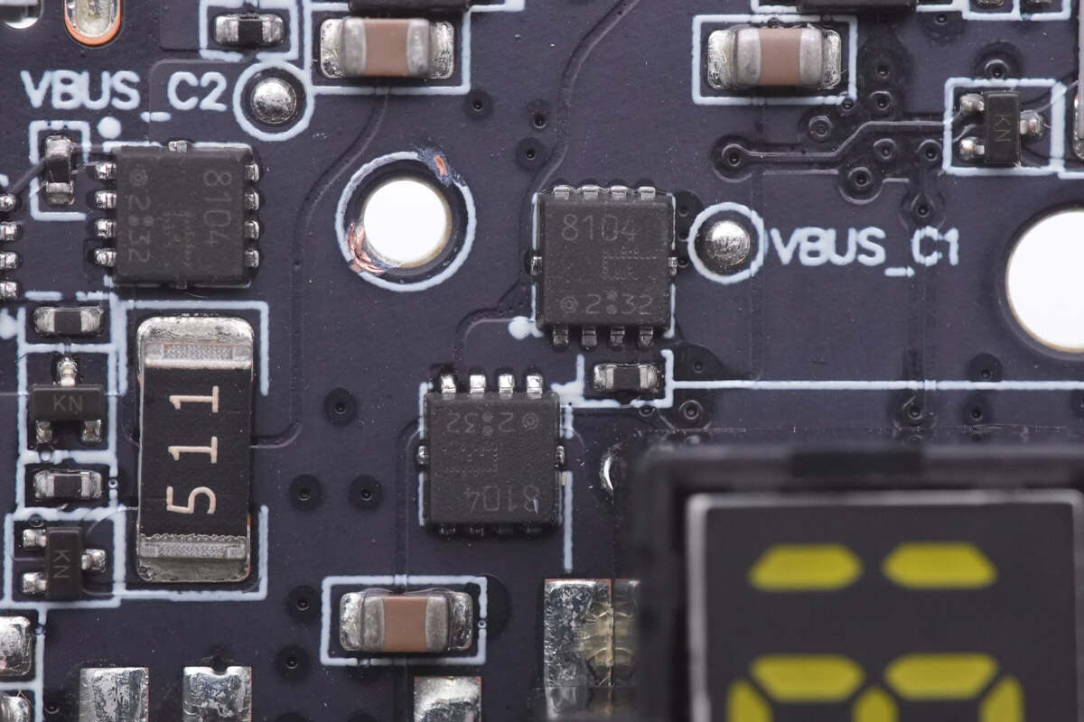
Two output VBUS MOSFETs of USB-C1 are from Toshiba. Model is TPCC8104.
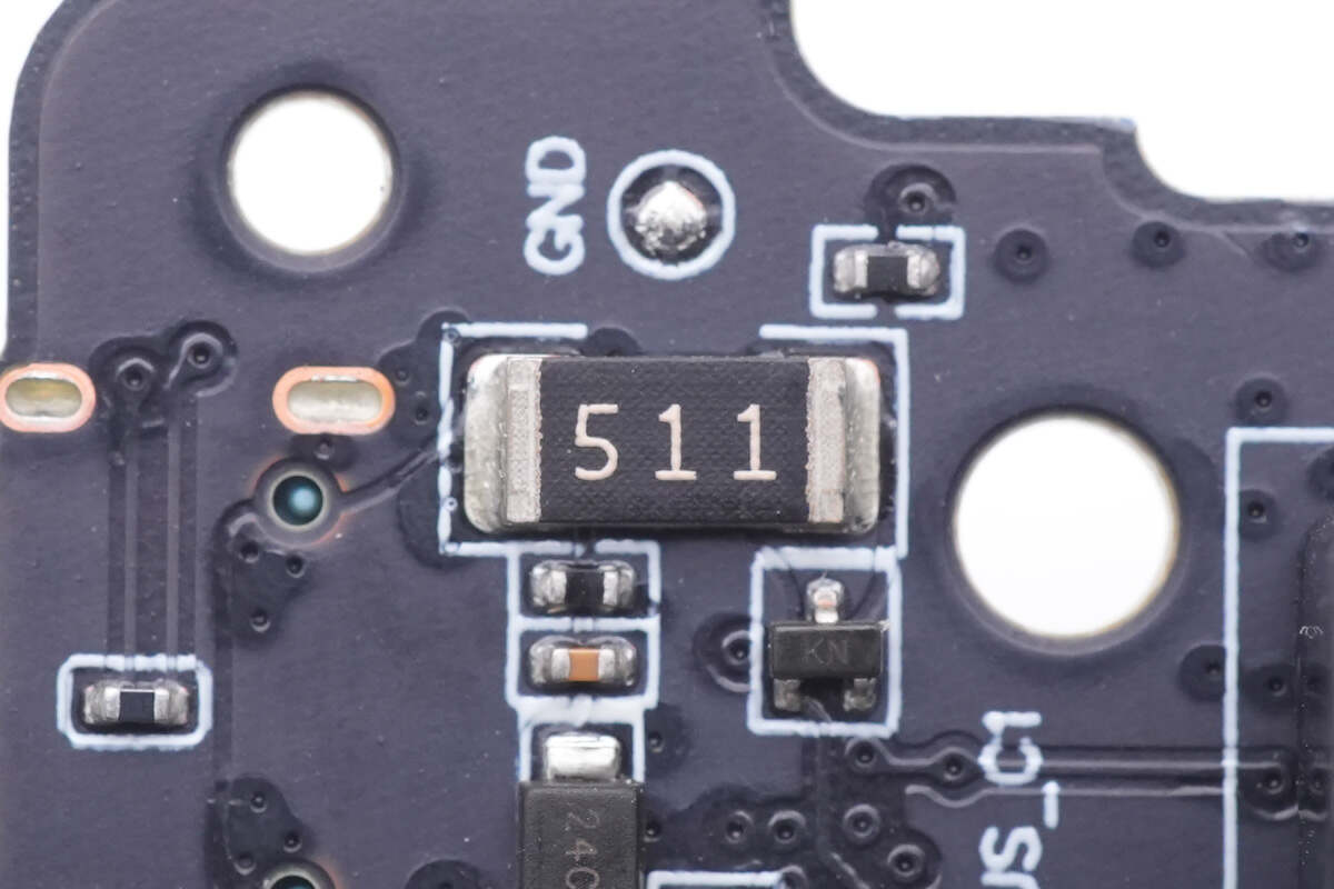
Another discharge resistor is used for the output of USB-C1. 510Ω.
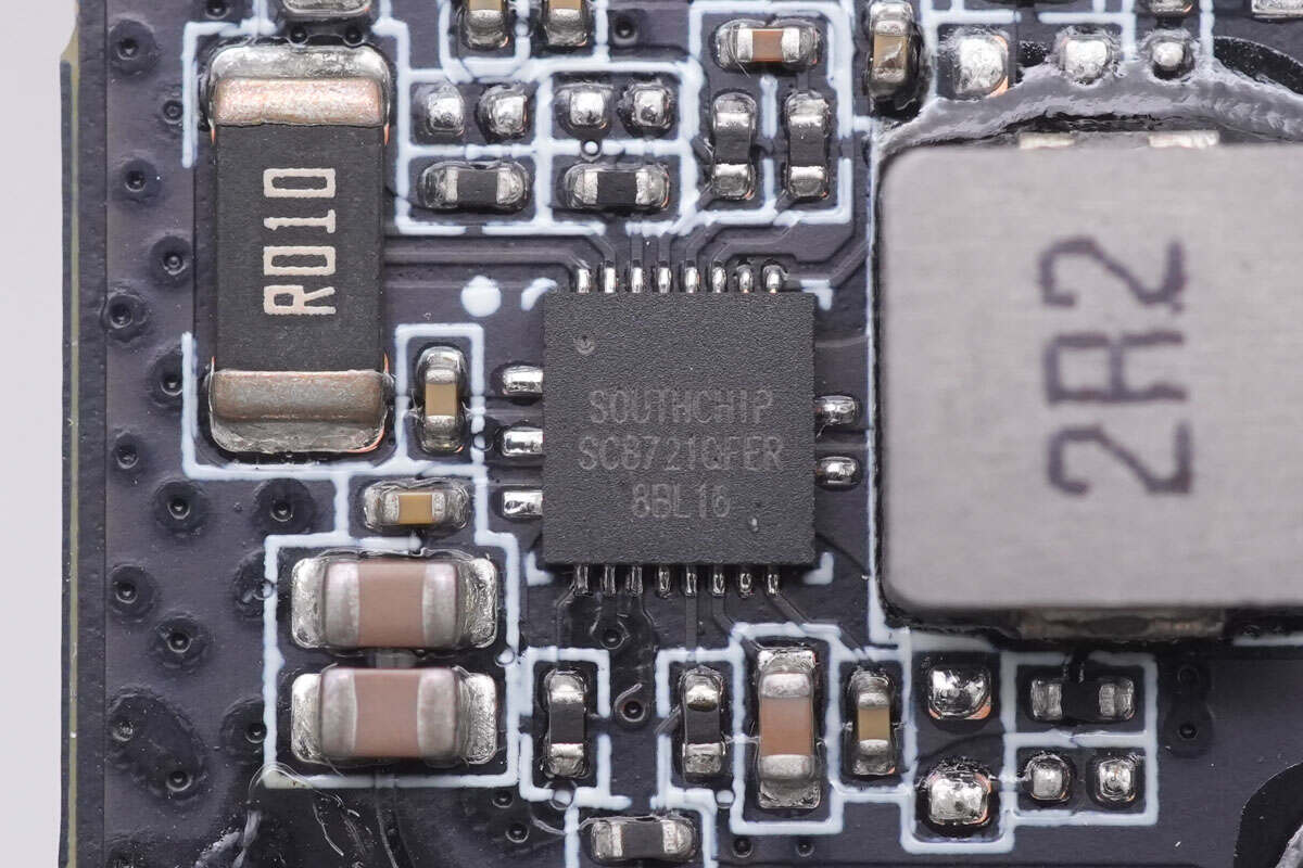
Then, move to the circuits of USB-C2 and USB-A.
The buck-boost converter is also from Southchip and adopts QFN 4x4 package. It integrates four MOSFETs and has multiple protection functions. It also supports wide input and output voltage range. Model is SC8721.
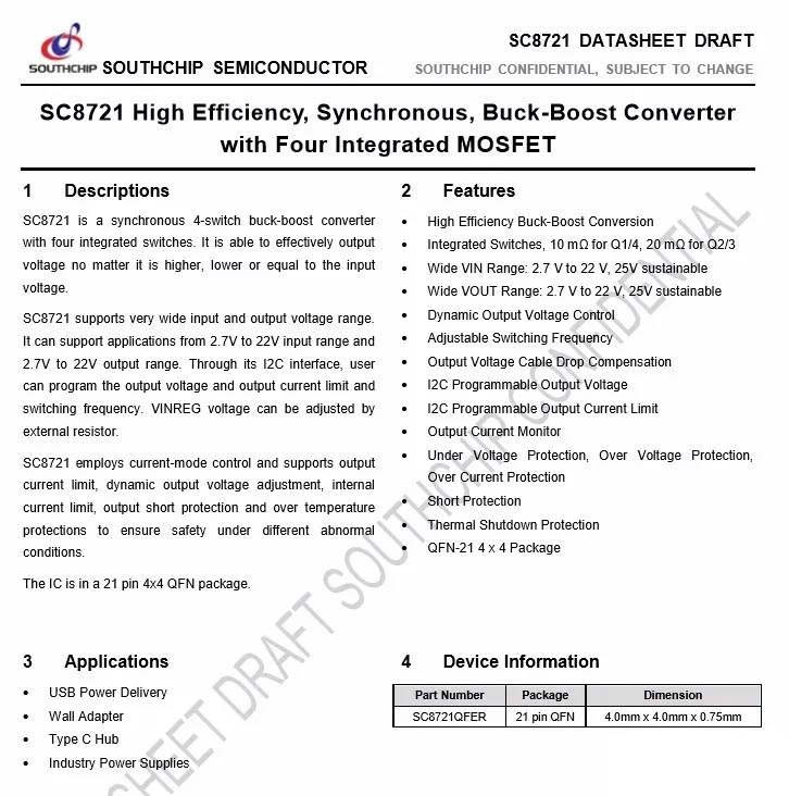
Here is all the information about Southchip SC8721.
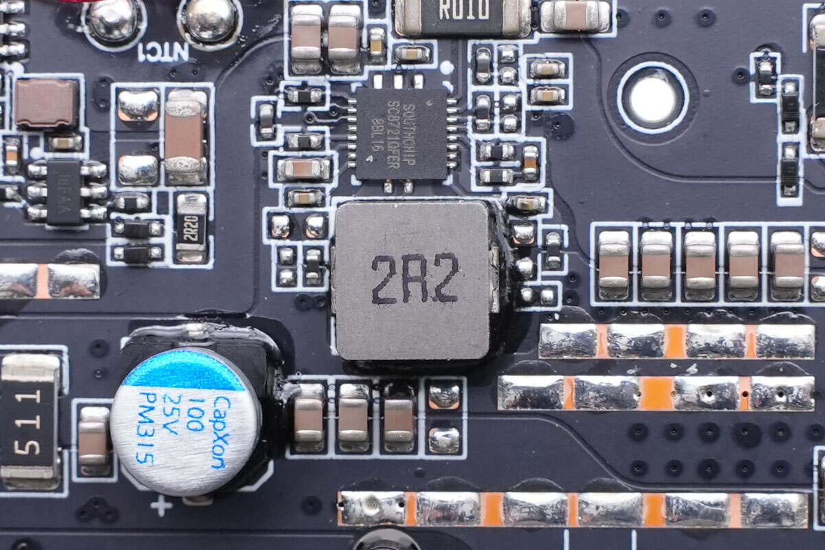
A 2.2μH alloy inductor is works with the SC8721.
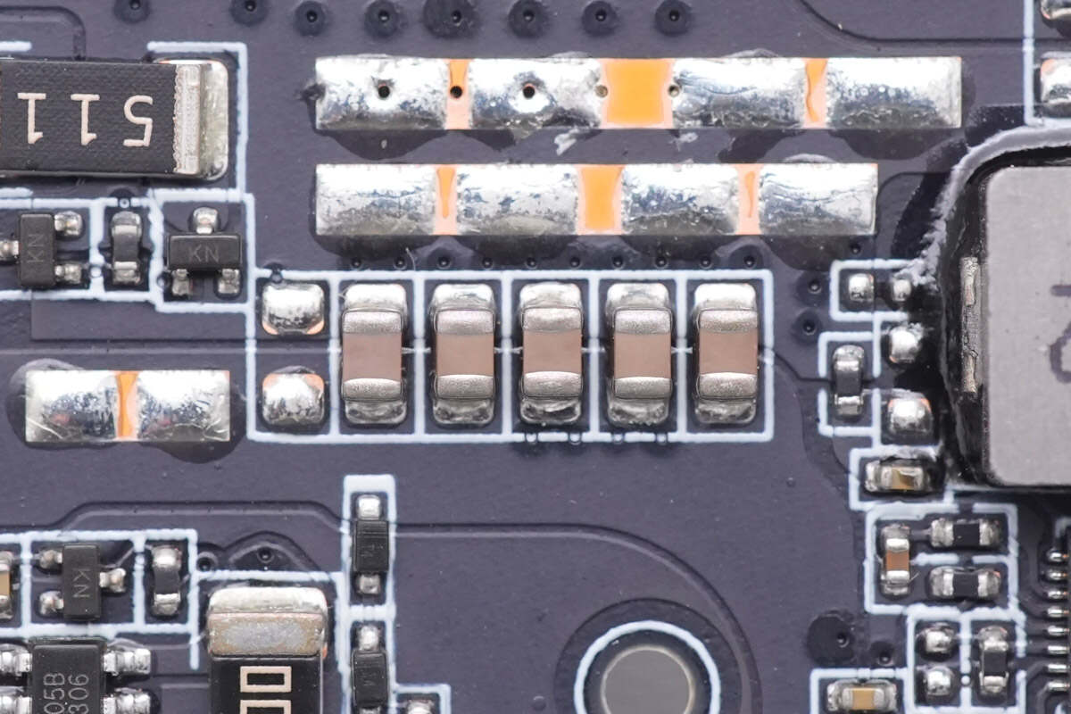
These five MLCC capacitors are connected in parallel for output filtering.
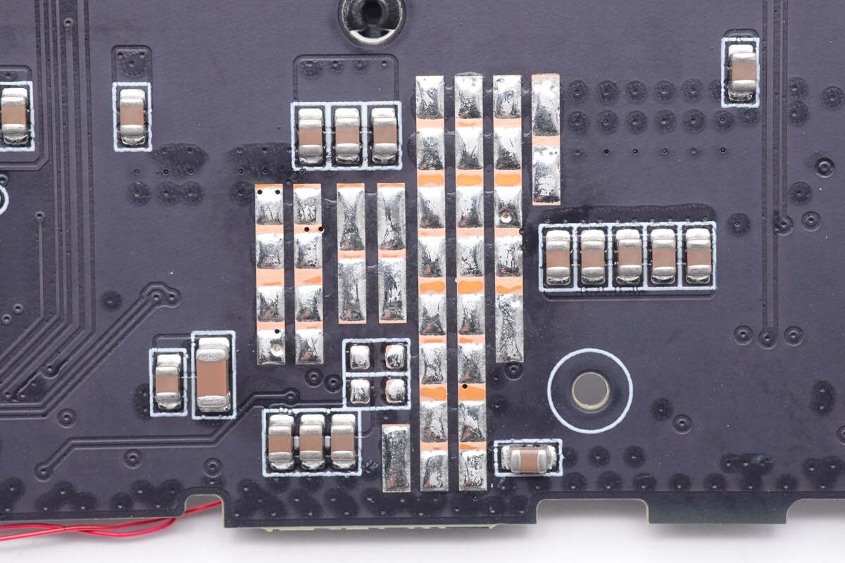
There are more MLCC capacitors on the back of the PCBA.
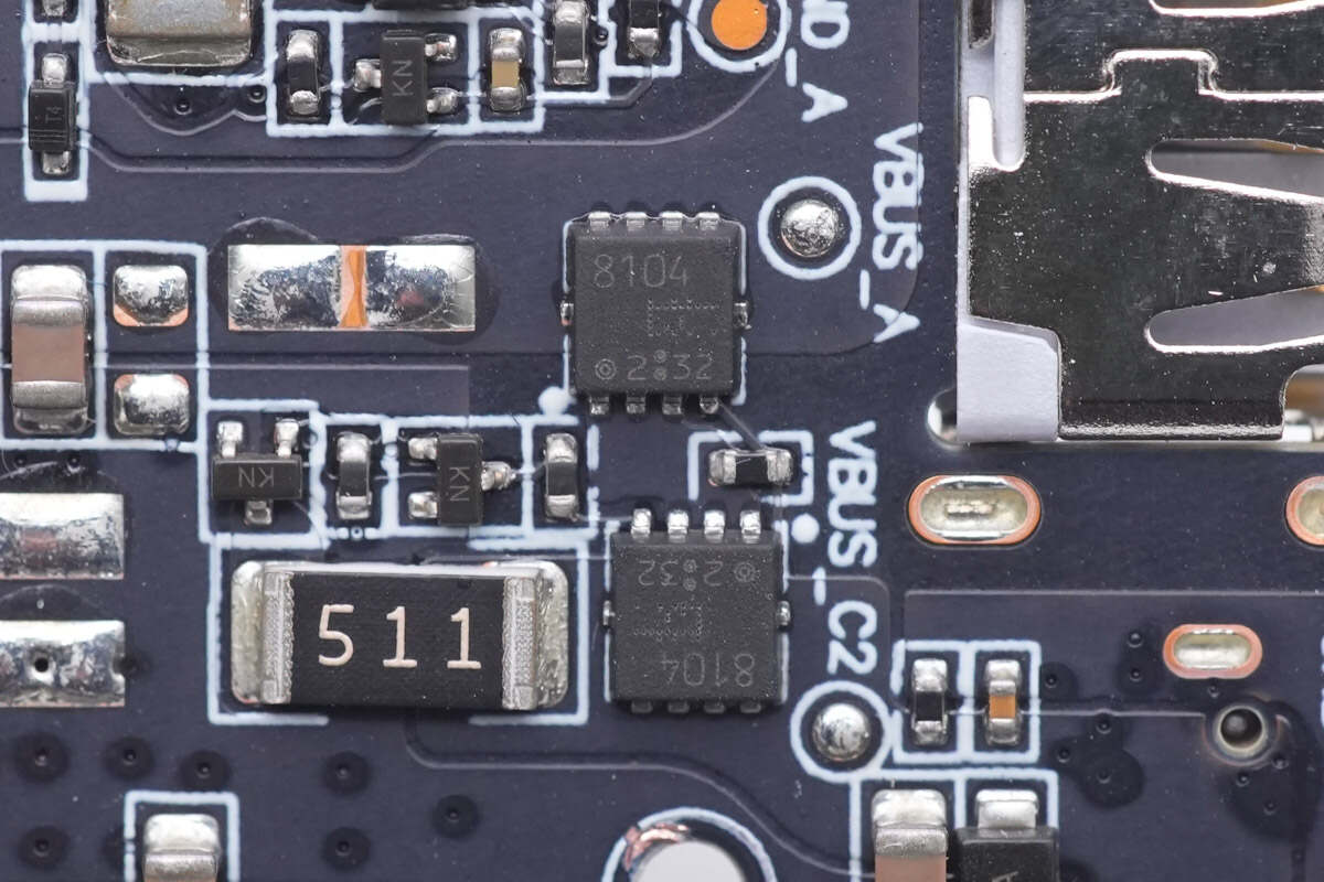
Those two output VBUS MOSFETs of USB-C2 are from Toshiba. Model is TPCC8104.
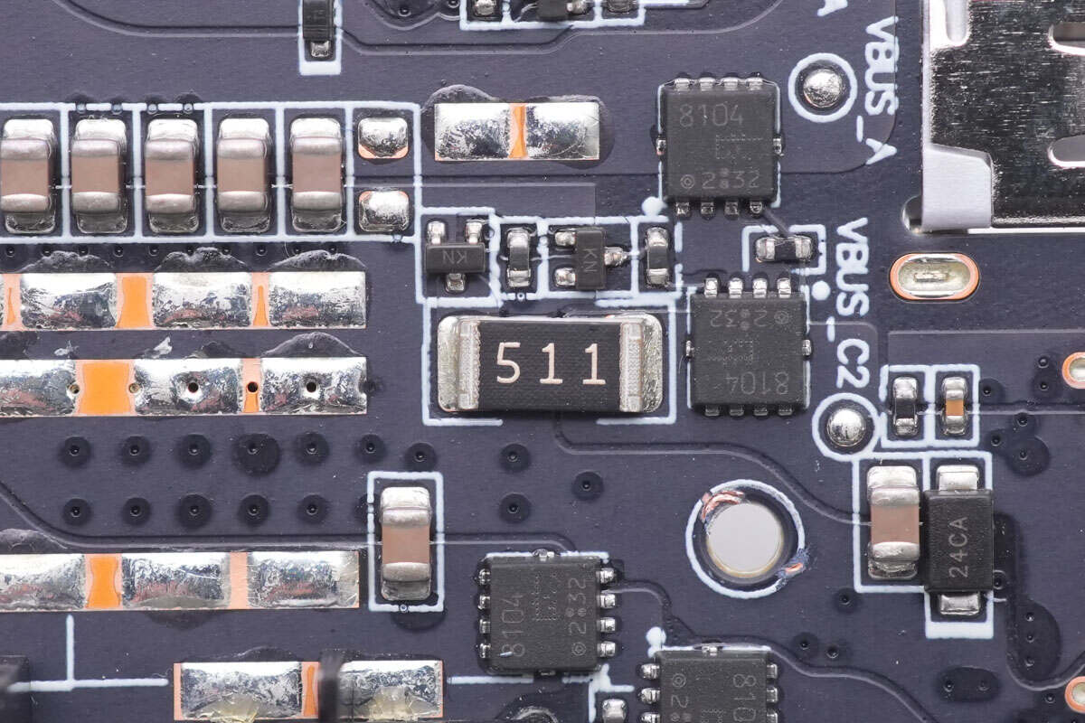
Another discharge resistor is used for the output of USB-C2. 510Ω.
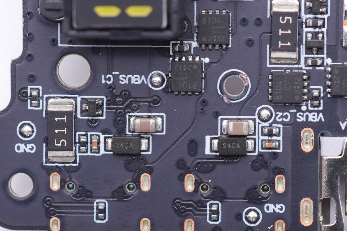
Both USB-C ports are equipped with TVS for overvoltage protection.
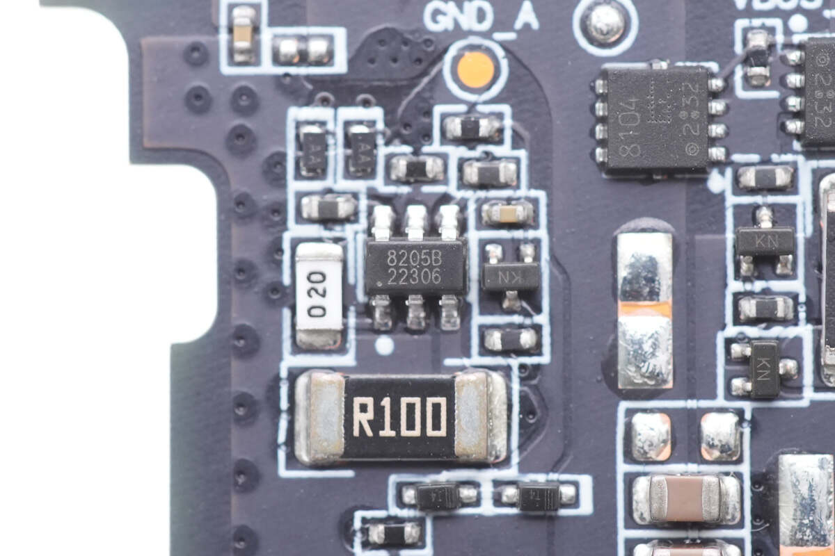
Here's the controller of switching circuit for USB-A.
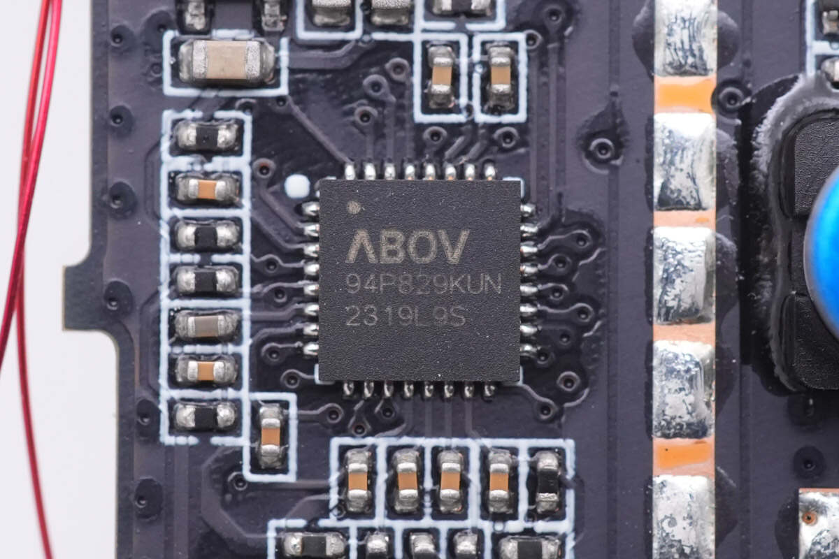
The MCU is from ABOV and integrates 8051 core. It can be regarded as protocol chip. And it supports PD3.1 and a wide range of other fast-charging protocols. Model is A94P829.
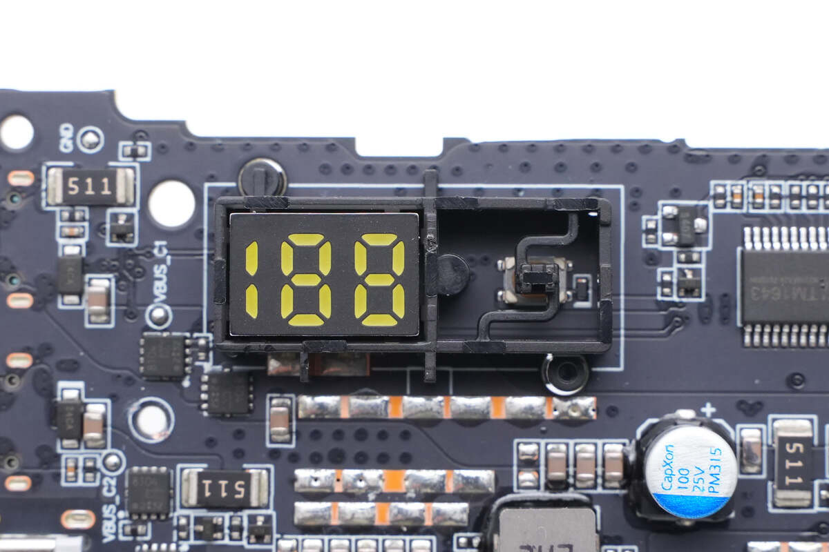
The segment LED display and power button are reinforced with a plastic frame.
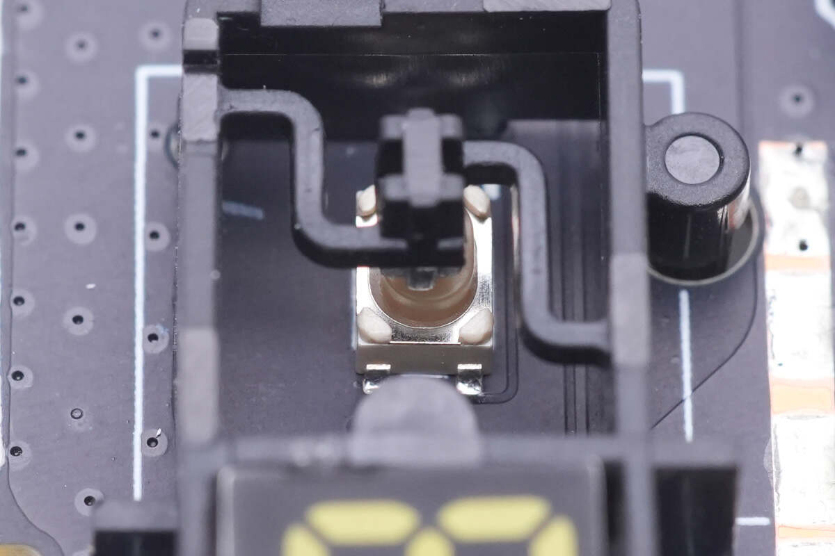
The power button is soldered on the PCB using SMD.
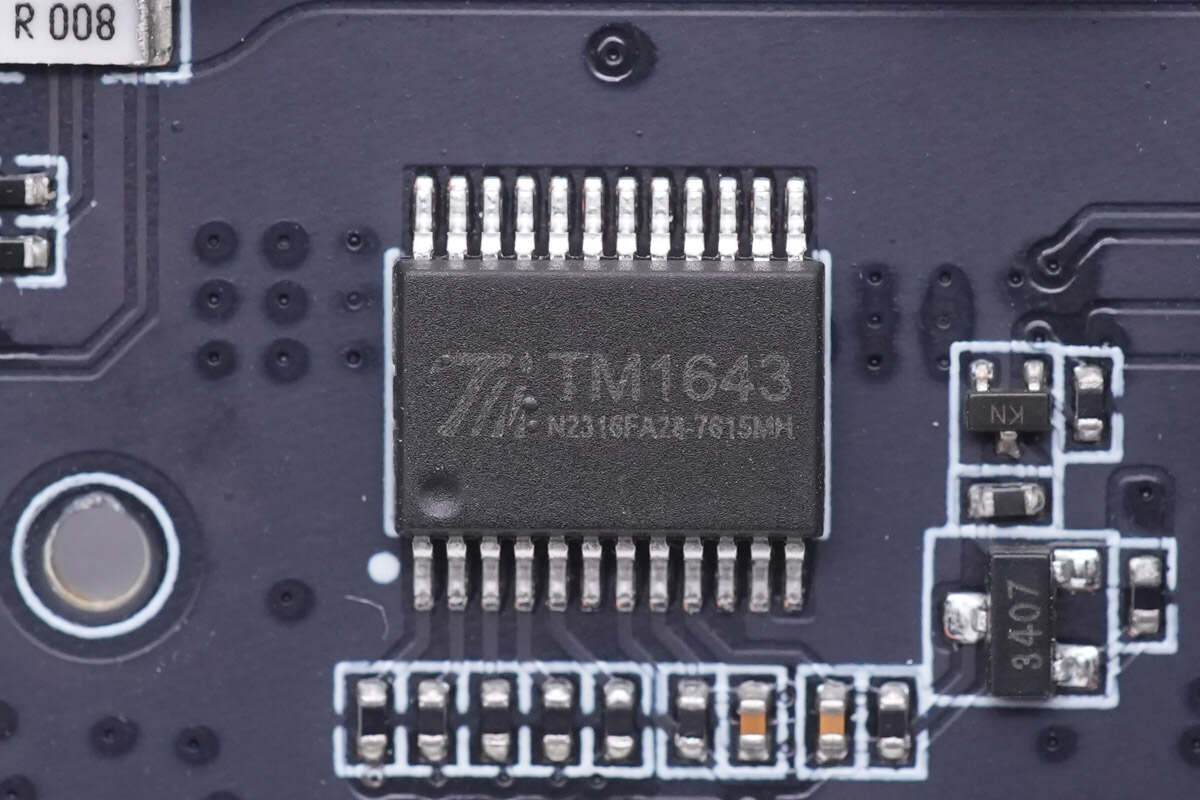
The LED driver IC is from Titan Micro. It supports 16 x 8 LED and can adjust display brightness via duty cycle. Model is TM1643.
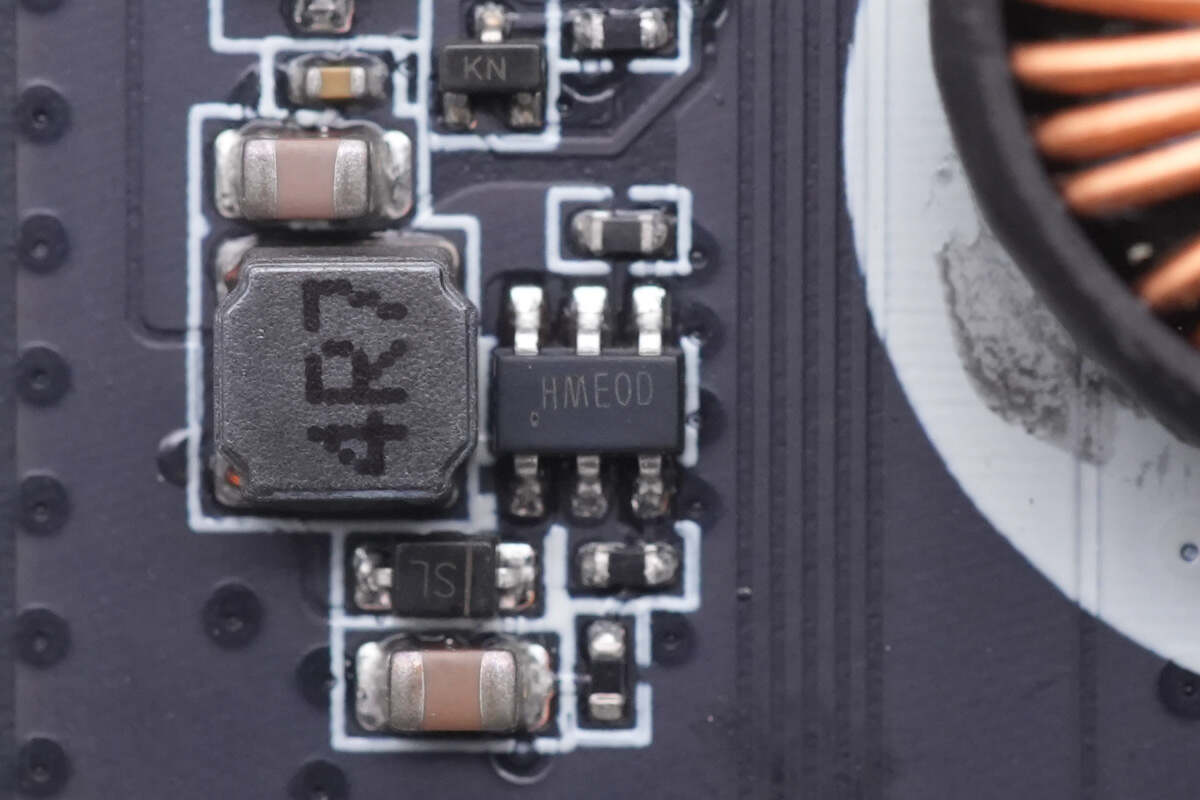
This tiny buck chip that powers the MCU is marked with HMEOD.
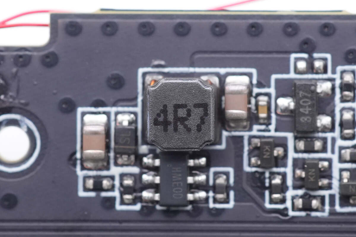
A 4.7μH inductor is next to it.
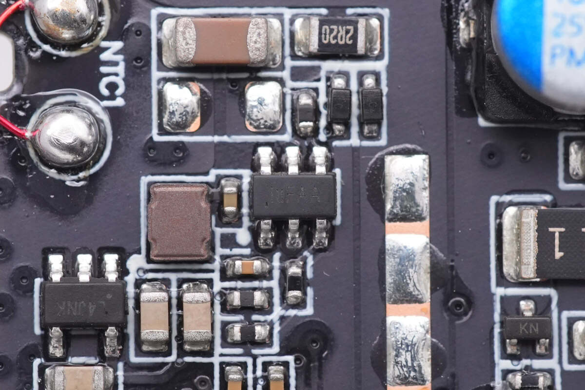
Another buck chip is marked with luFAA.
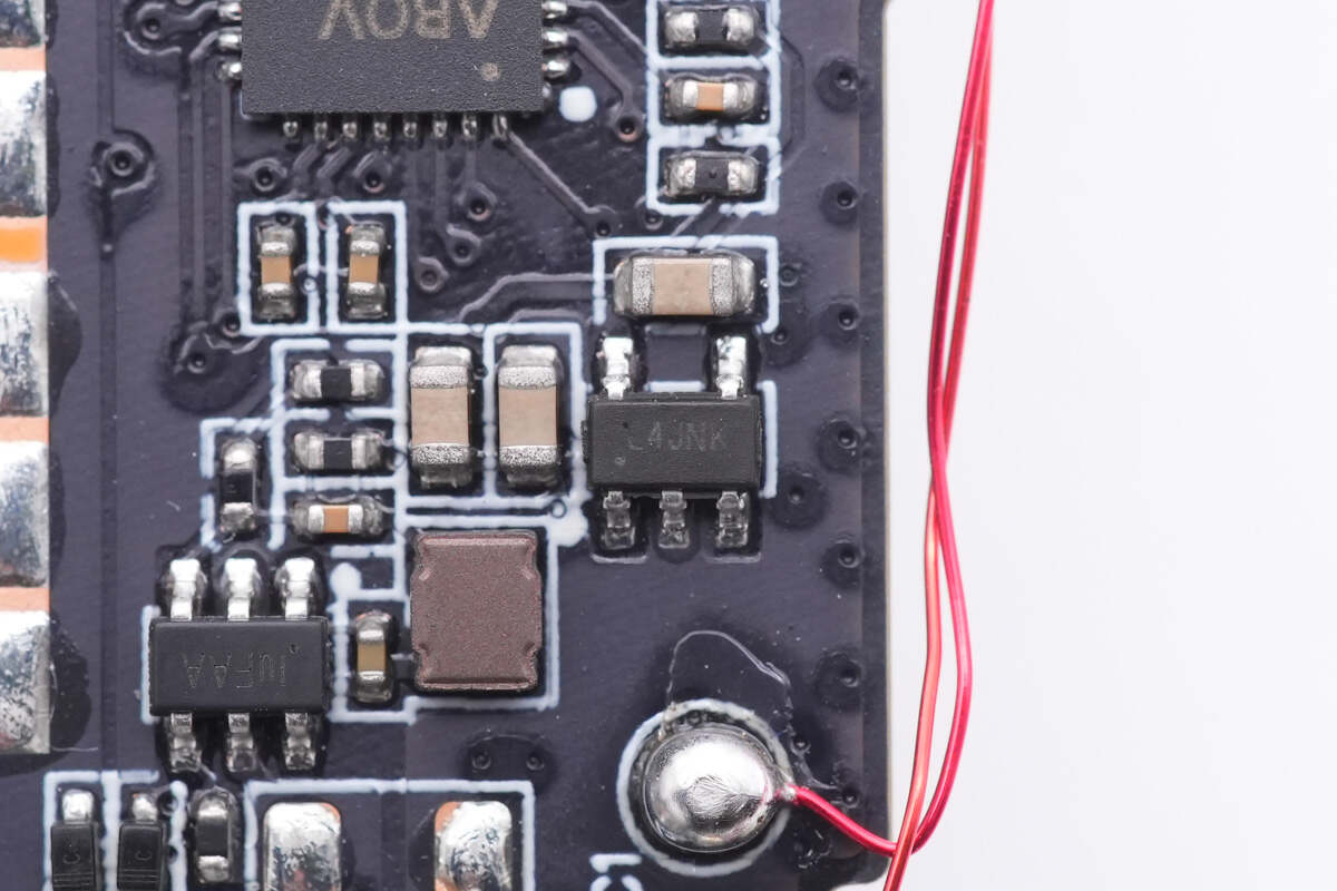
The voltage regulator is marked with L4JNK.
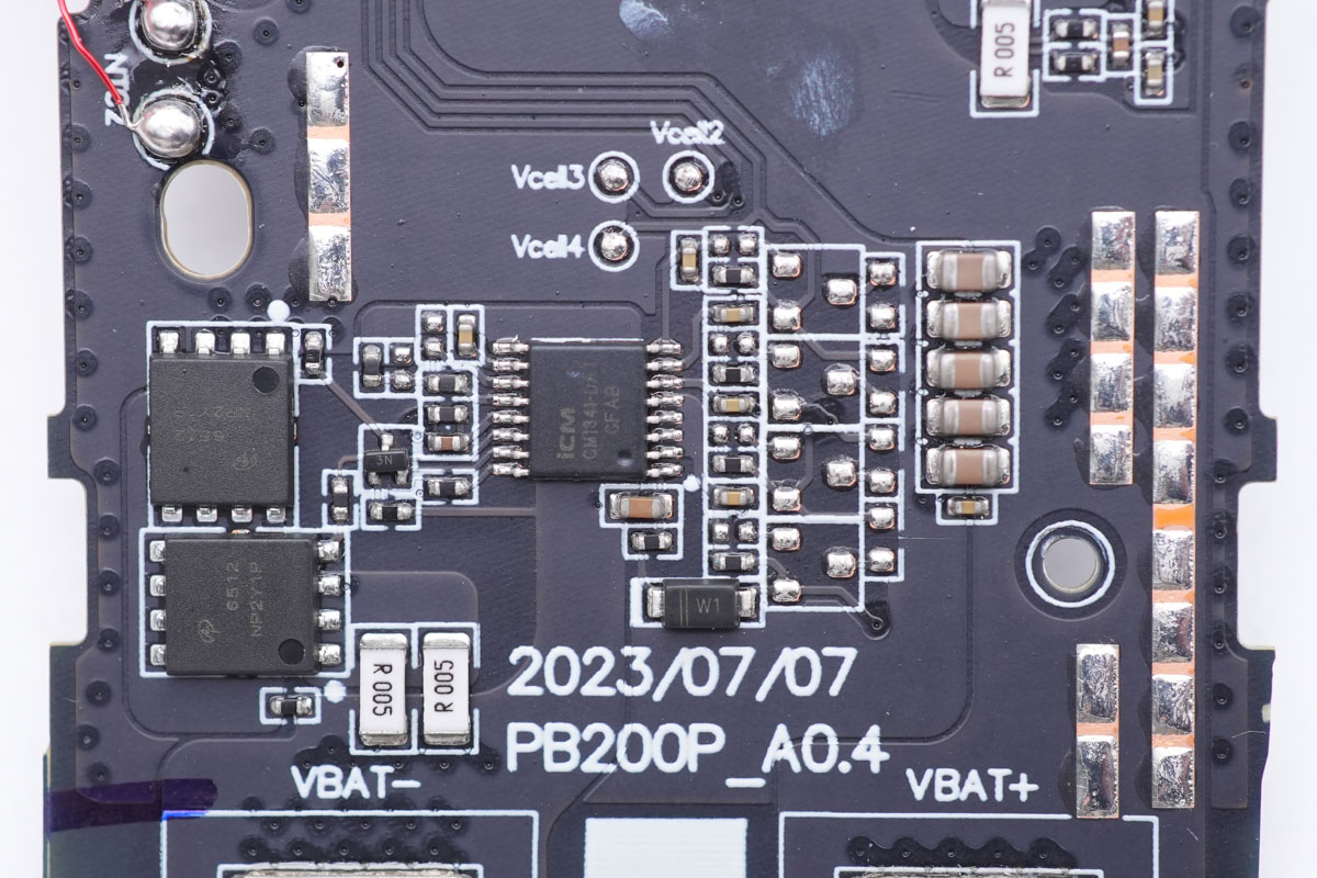
Here is the battery protection circuit.
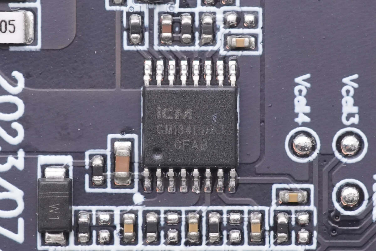
The battery protection chip is from iCM, model CM1341-DAT, it supports lithium iron phosphate batteries and integrates high-precision voltage & current detection circuits.
It can also achieve functions such as overcharging, over-discharging, short-circuit, and over-temperature protection by monitoring battery voltage, current, and temperature information, with other built-in protection features and delays.
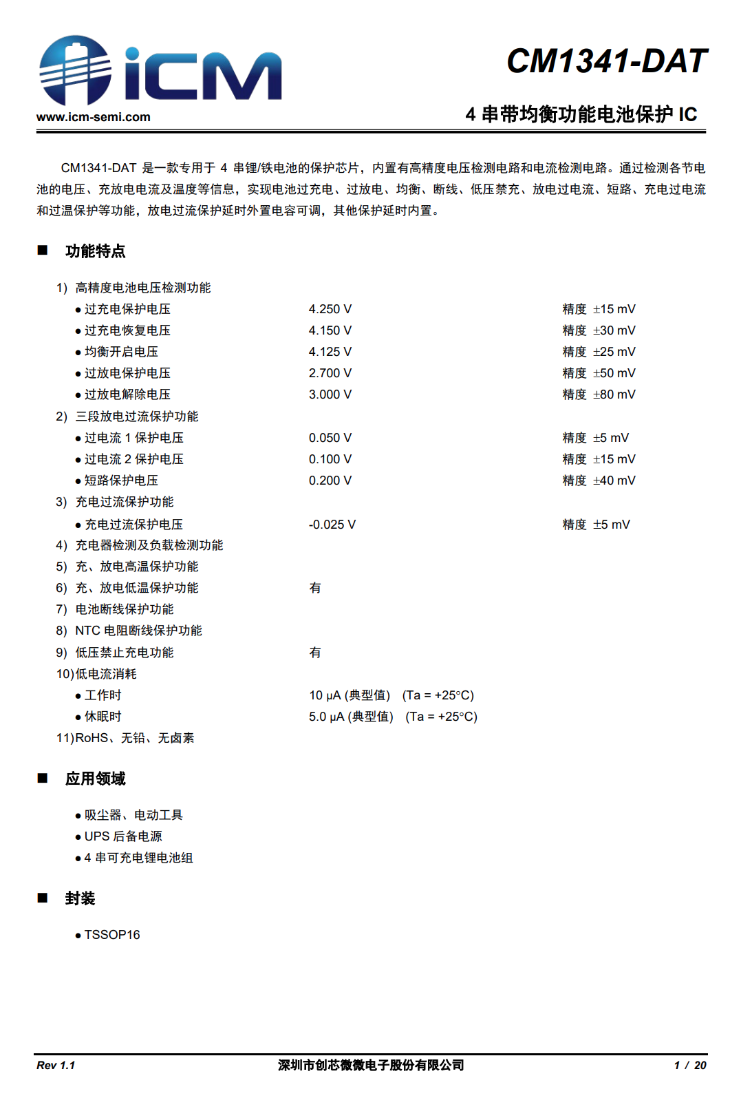
Here is all the information about iCM CM1341-DAT.
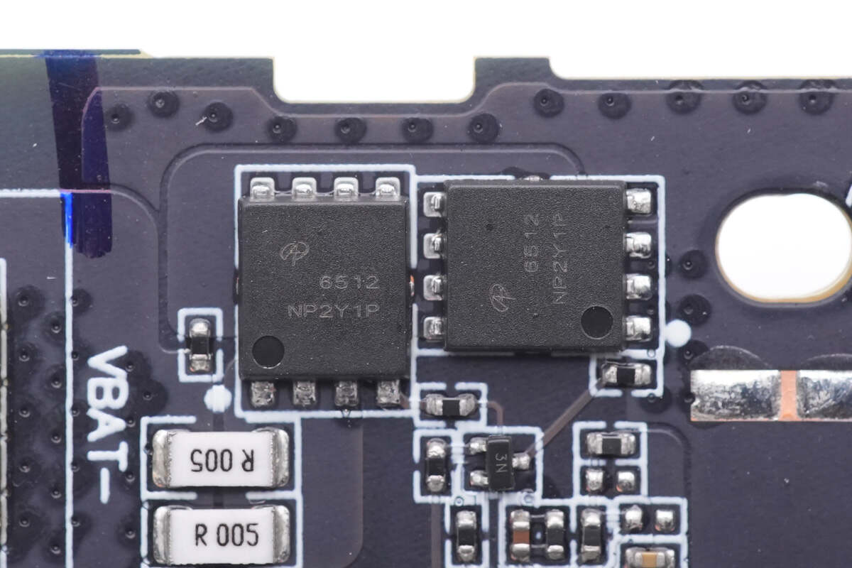
Two protection MOSFETs for battery cells are from AOS and adopt DFN5 x 6 package. 30V, 1.4mΩ. Model is AON6512.
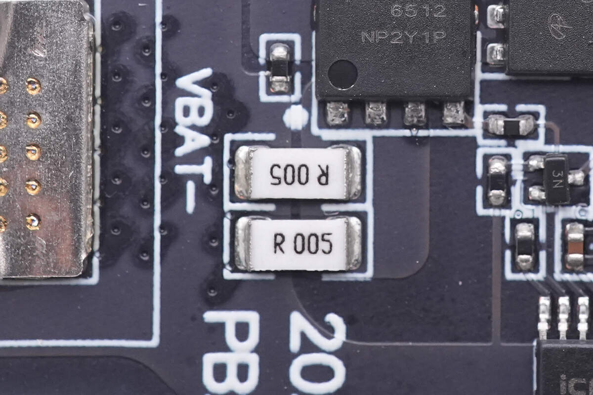
Two 5mΩ resistors are connected in parallel for current detection.
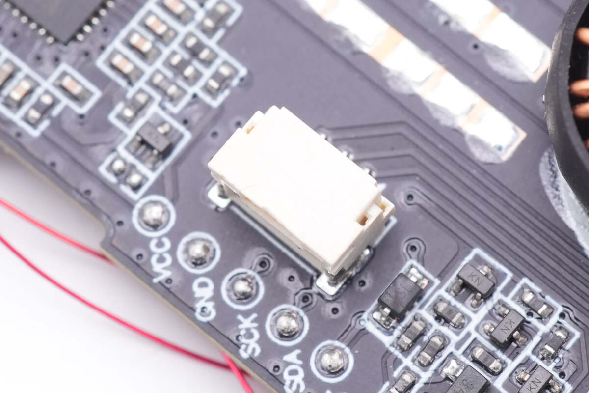
This is the connector for single cell voltage sensing.
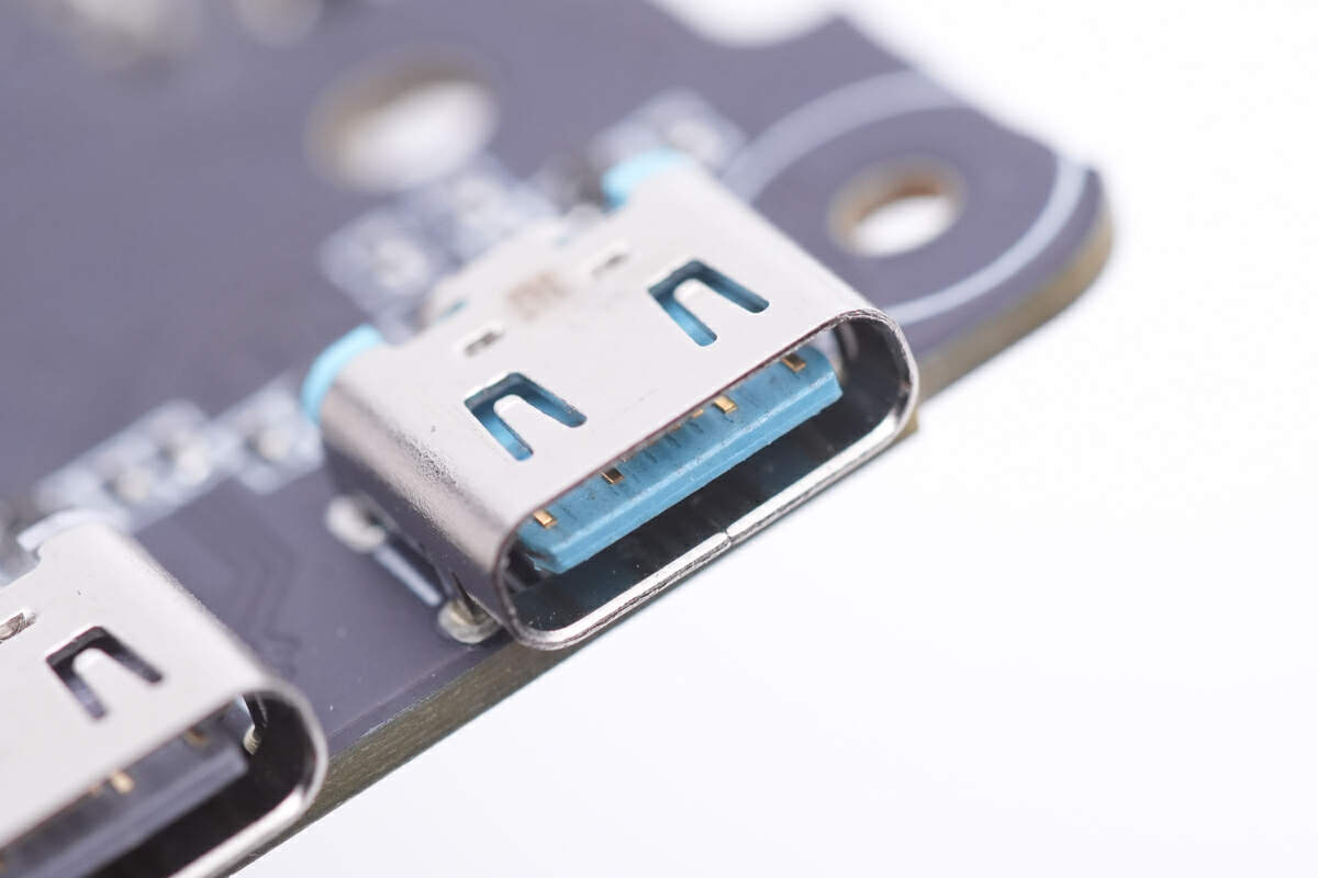
The color of USB-C1 is different from USB-C2.
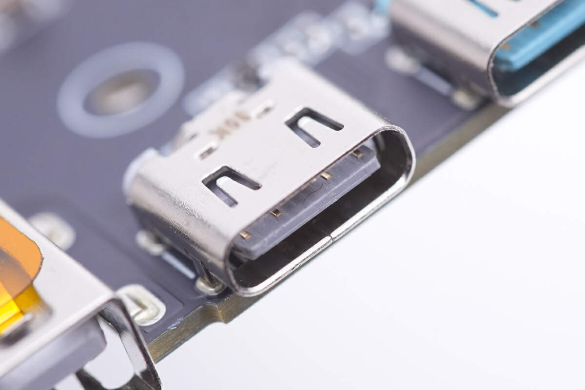
You can distinguish them more intuitively.
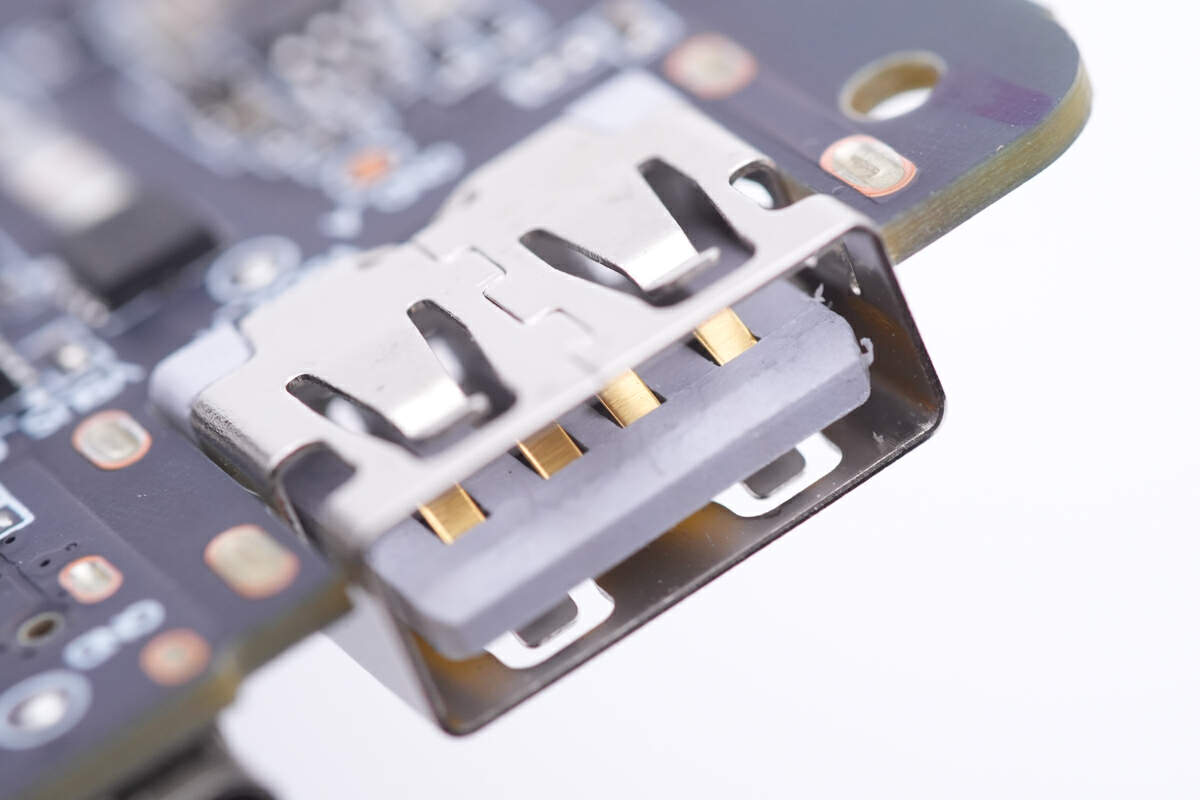
And the USB-A is soldered on the hollow of the PCB to reduce thickness.
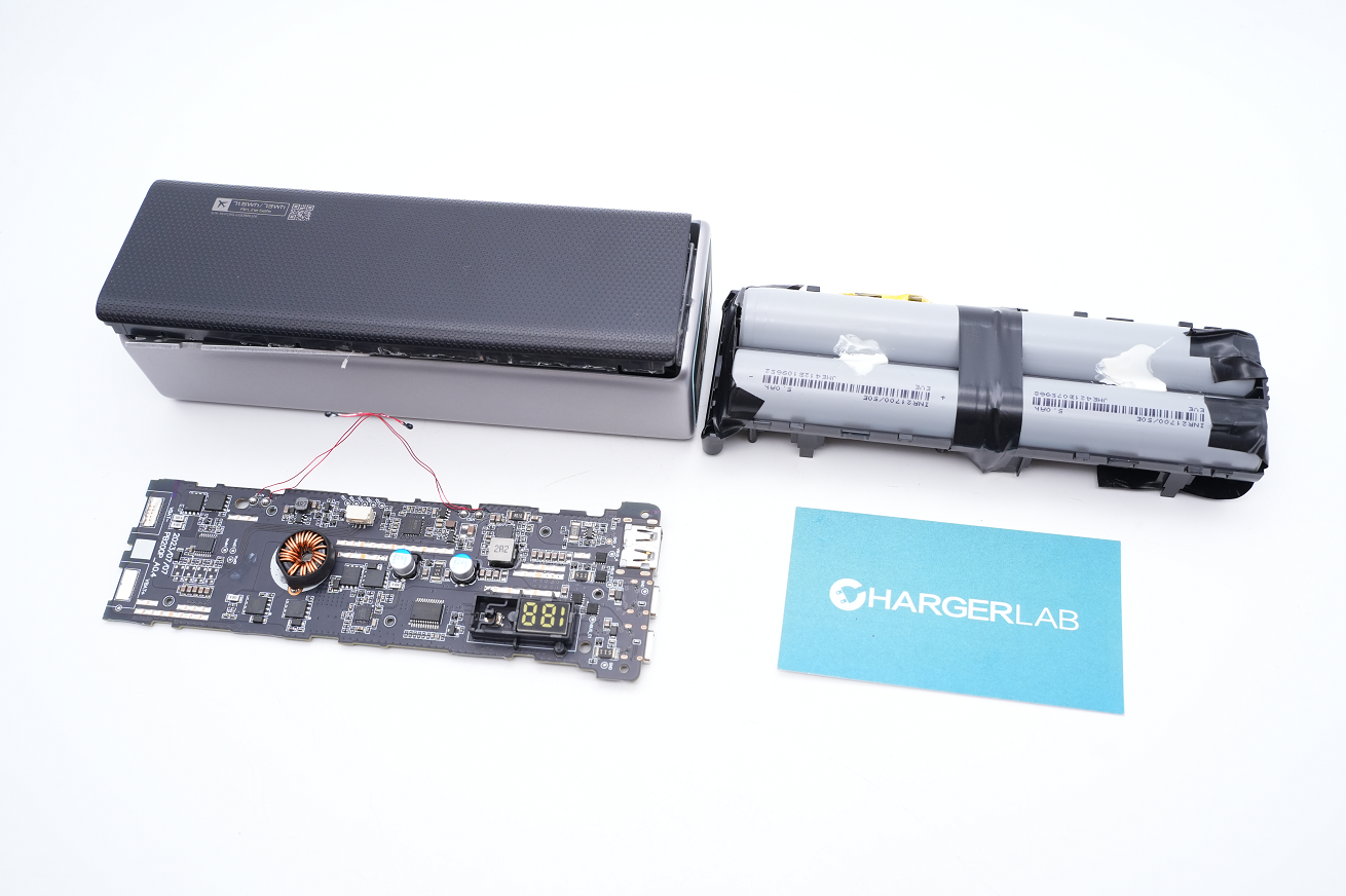
Well, that's all components of the CUKTECH 150W power bank.
Summary of ChargerLAB
As an affordable option, it does not support USB PD3.1. But the PD output power of USB-C1 can still reach 100W.
Even though performance is compromised, its quality does not. It integrates four battery cells and two independent buck-boost circuits. The all-black PCB and thick aluminum plate make it more solid.
Related Articles:
1. Teardown of CUKTECH No.15 150W & 20000mAh Power Bank (Video)
2. Teardown of CUKTECH No.30 PD3.1 & 300W Power Bank
3. Teardown of Anker 140W PD3.1 Power Bank (737 Power Bank)


