Introduction
ChargerLAB has gotten a new Lighter 65W GaN fast charger AC65B launched by CukTech recently, with a thickness of only 14.5mm (0.57 inches) and a power density of 1.41W/cm³. Let's take it apart.
Unboxing

The front of the box is printed with the CukTech logo, product name, appearance and the GaN3 icon, showing this is a GaN charger.

In the back are the product parameters and manufacturer information.

This is the close-up.

The CukTech logo is printed on the side.

The package includes the charger and user manual.

The CukTech charger is very flat. Its shell is made of white flame retardant material.

The CukTech and Lighter 65W are printed on the front of the charger.

There is a design of diagonal stripes embossing near the output area.

The other side is printed with the slogan and the parameters.

There are the parameters.
Model: AC65B
Input 1: 100-130V~50/60Hz 1.5A
Output 1: 5V3A, 9V3A, 12V3A, 15V3A, 20V2.25A (45W Max)
Input 2: 200-240V~50/60Hz 1.2A
Output 2: 5V3A, 9V3A, 12V3A, 15V3A, 20V3.25A (65W Max)

It adopts the foldable prongs.

It is equipped with a single red USB-C port.


Its size is about 71.58 X 43.93 X 14.62 mm (2.81 X 1.72 X 0.57 inches). The volume of the charger is about 45.97cm³ (2.8 in³), and the power density is 1.41W/cm³.

Compared with the Apple 61W charger, the CukTech 65W is much smaller.

That's what the charger looks like in my hand.

Its net weight is about 77g (2.71oz).

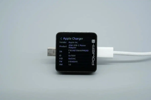
The ChargerLAB POWER-Z KT002 finds that the USB-C port supports Apple 2.4A, Samsung 5V2A, DCP protocol, QC2.0/3.0, AFC, FCP and PD3.0 fast charging protocol.

The USB-C port also supports five fixed PDOs of 5V3A / 9V3A / 12V3A / 15V3A / 20V3.25.

It is 8.93V 2.94A 26.24W when the charger is charging the iPhone 13 Pro Max.

When charging the MacBook, the power is 63.4W.
Teardown

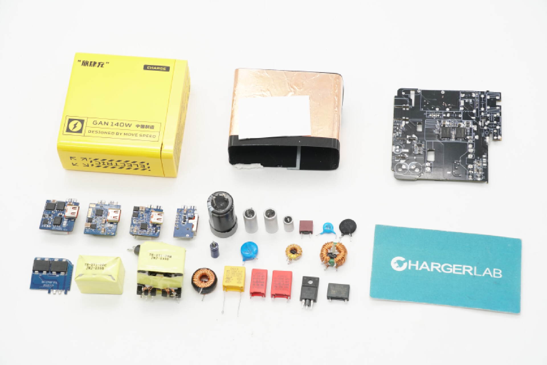
Open the shell, and we can see the ultrasonic soldering package. The white glue is filled on both sides of the PCBA module for reinforcement.

Then, take out the PCBA module.

The back of the module is covered with copper to help lose heat, and two high-voltage filter electrolytic capacitors are placed inside the space on either side of the foldable prongs to lower the thickness.

Insulating tape is pasted on the edges and inside of the two heatsinks, which are soldered on the PCB, and a conductive fabric is pasted between the two heatsinks.

PCBA module and prongs are powered by PCB and leaf spring, and two terminals are gilded.


The PCBA module's size is about 44.38 X 10.79 X 39.5 mm (1.74 X 0.42 X 1.55 inches).

In addition, the length of the module plus the capacitor is 65.32mm (2.57 inches).

Below the heatsink are two plastic pieces to insulate the transformer, one of which is also exposed and coated with the thermal adhesive. The gap is filled with the blue thermal pad to help components lose heat.

The front of the module is equipped with the SMD fuse, filter capacitor, filter inductor, optocoupler and other components.

The other side is equipped with the bridge rectifier, primary and secondary switching power controllers, MOSFET, protocol chip, etc.

The planar transformer is placed directly on the PCB at a higher cost, with better heat dissipation. We also found that the charger adopts the high-frequency QR power solution, and the protocol chip controls the output voltage through optocoupler feedback.

The fuse is from Betterfuse, rated at 3.15A. The current first pass through the SMD fuse and will be fused to protect the circuit if there is an overcurrent.

The current then passes through the SMD common mode choke to filter the electromagnetic interference.

There is also a high voltage MLCC filter with 2220 package.

There is a filter inductor.

After filtering the EMI, the AC is converted to pulsed DC by the Yangjie RYBSM6010H bridge rectifier.

The pulsed DC is then filtered into DC by two high voltage filter electrolytic capacitors, both from BERYL, with 400V 27μF.

Two BERYL electrolytic capacitors have a total capacity of 54μF.

The PWM controller from Kiwi Instruments KP2202 integrated AC input power-down detection and X-capacitor discharging function. It has ±1% constant voltage accuracy, low starting/working current, and standby power consumption is less than 30mW.
The maximum operating frequency of KP2202 is adjustable at 500kHz, 300kHz and 140kHz; the VDD supply voltage range is 10-112V; the chip integrates comprehensive protections, and the built-in driver can drive CoolMos and GaN switch transistors.

The GaN IC comes from Navita NV6134A and adopts 6*8mm QFN package. It integrates a driver and lossless current sampling circuit. It supports the 2MHz switching frequency. And the resistor is 260mΩ. Withstand voltage is 650V.

Here are the details of the Navitas NV6134A.

The planar transformer is made of a PCB board with a label on the side of the core, bearing the TEC26004 and QR.

There is a blue thermal pad inside the core.

Let's smash the planar transformer to make it clear.

The EL 1018 optocoupler is used for output voltage adjustment and feedback. It changes the luminous intensity of the diode inside the optocoupler through the protocol chip and changes the conductivity of the phototransistor inside the optocoupler.

Four SMD Y capacitors are from Holy Stone.
The AC output from the planar transformer is synchronously rectified and converted to pulsed DC.

The synchronous rectifier controller adopts the Southchip Semiconductor SC3503.

Here are the details of the Southchip Semiconductor SC3503.

The synchronous rectifier is from AOS, model AON6220, an NMOS that withstands the voltage of 100V, with a thermal resistance of 5.1mΩ and a DFN5*6 package.


The pulsed DC is filtered into DC by the solid capacitors, both of which are also from BERYL, with specifications of 25V 270μF.

The USB PD protocol chip is the Weltrend WT6636F, which is a protocol chip certified by USB-IF's USB PD3.0 (PPS) (TID No. 1080018), and additionally had a Qualcomm QC4+ certification with the number QC20200316138. The WT6636F supports USB PD3.0 and PPS and has a built-in programmable constant-current constant-voltage controller.

The output VBUS switch transistor is the AOS AON7534, an NMOS that withstands 30V and has a thermal resistance of 4.1mΩ and a package of DFN3*3.

Here is the USB-C receptacle soldered by a via.

The USB-C receptacle is from KRCONN.

OK, that's all for the teardown of the new CukTech Lighter 65W GaN charger AC65B.
Summary of ChargerLAB
The CukTech Lighter 65W GaN charger adopts the GaN technology, making it small and flat. With the foldable prongs, it is very suitable for travel. The charger supports QC2.0/3.0, AFC, FCP, and PD3.0 fast charging protocols and has a full range of voltage levels from 5-20V to meet the charging needs of laptops and power banks.
The components used are from well-known manufacturers. It adopts the BERYL electrolytic capacitors, the Kiwi Instruments KP2202 PWM controller, Navitas GaN power chip, four Holy Stone SMD Y capacitors, Southchip Semiconductor SC3503, AOS AON6220, Weltrend WT6636F USB PD protocol chip, etc.
Related Articles:
1. Review of Asus Adol 100W GaN Charger
2. Teardown of Anker 100W USB-C Charger, 736 Charger (Nano II 100W)
3. Review of UGREEN Nexode 3-in-1 65W GaN Charger

