Introduction
Apple announced new products and updated their operating systems at WWDC2023. ChargerLAB found Apple also listed a brand new 70W power adapter on its official website. We’ve posted the Compatibility 100 Test for this charger, you can click the related articles to check that out.
And today, we're going to take it apart to see how it differs from other Apple chargers we’ve taken apart before.
Product Appearance
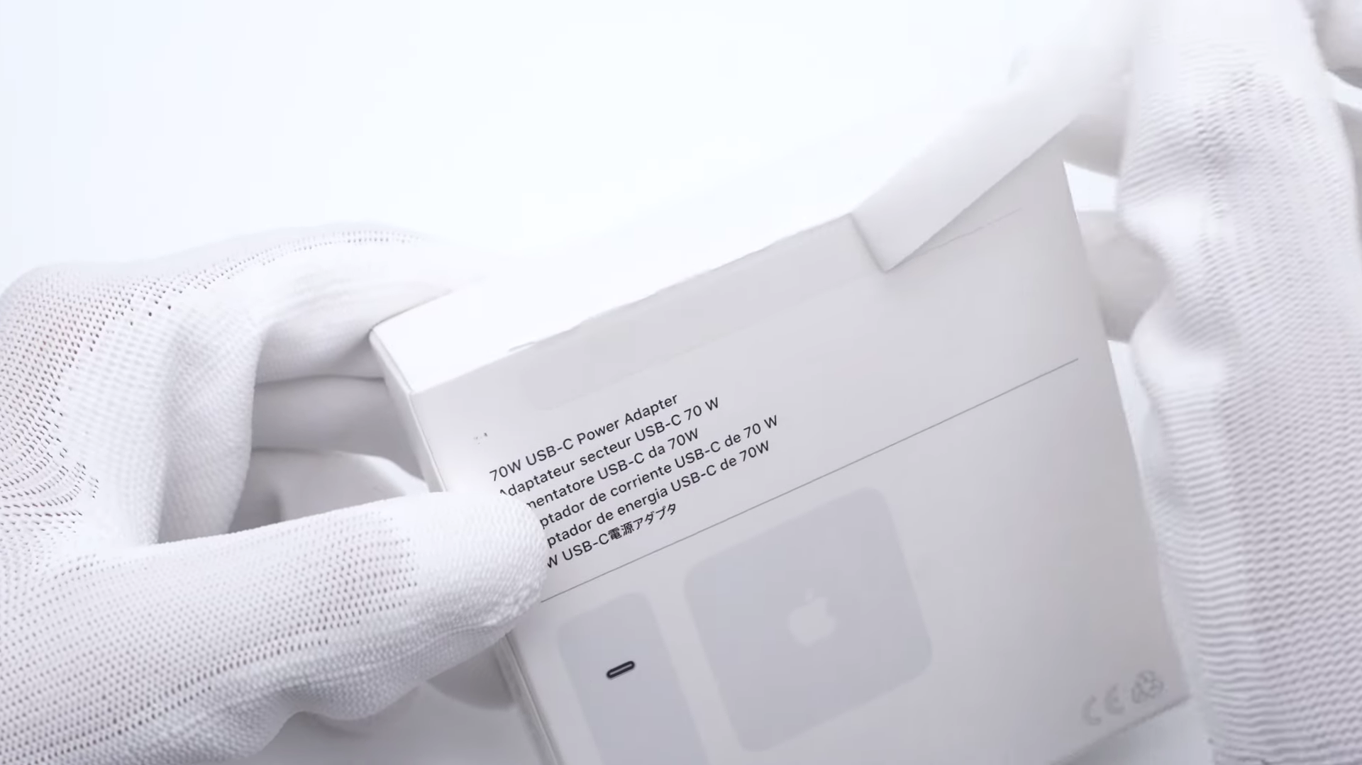
Let’s tear off the sealing strip.
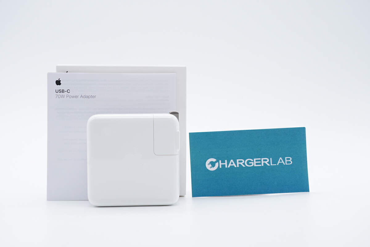
Like always, it only contains a charger and some documents without any cable.
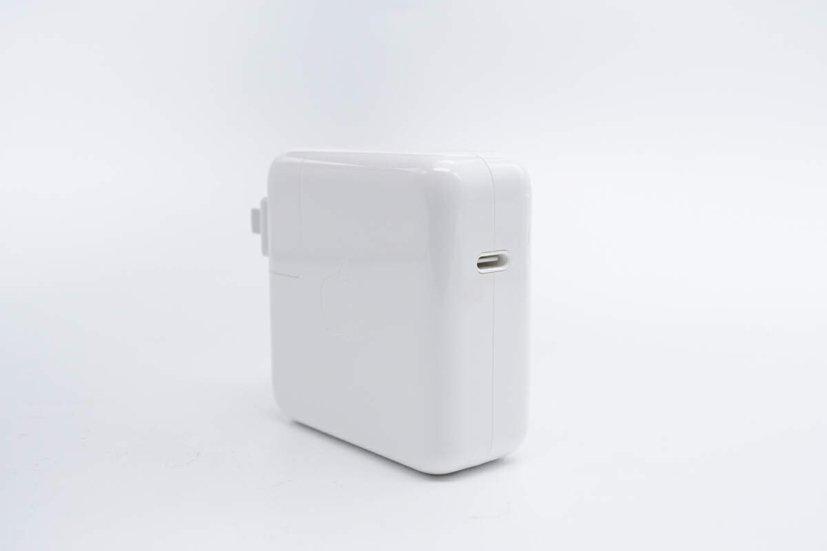
It adopts a classic white square design with glossy surface.
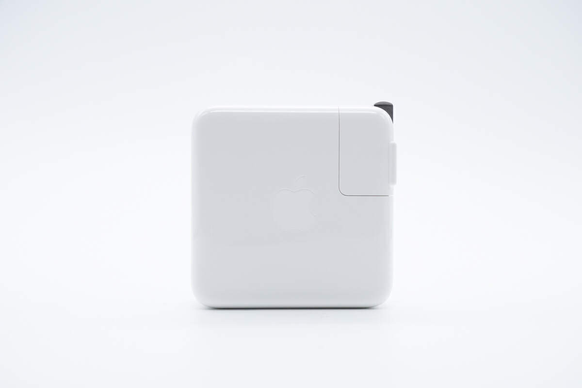
The Apple logo is engraved on the front.
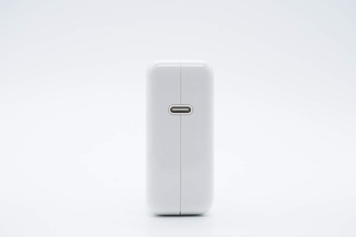
And it’s equipped with a USB-C port.
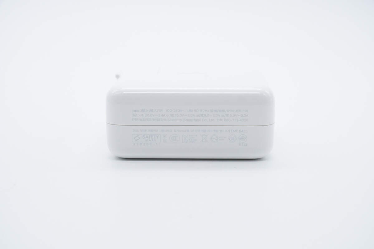
All specs info are printed on the side.
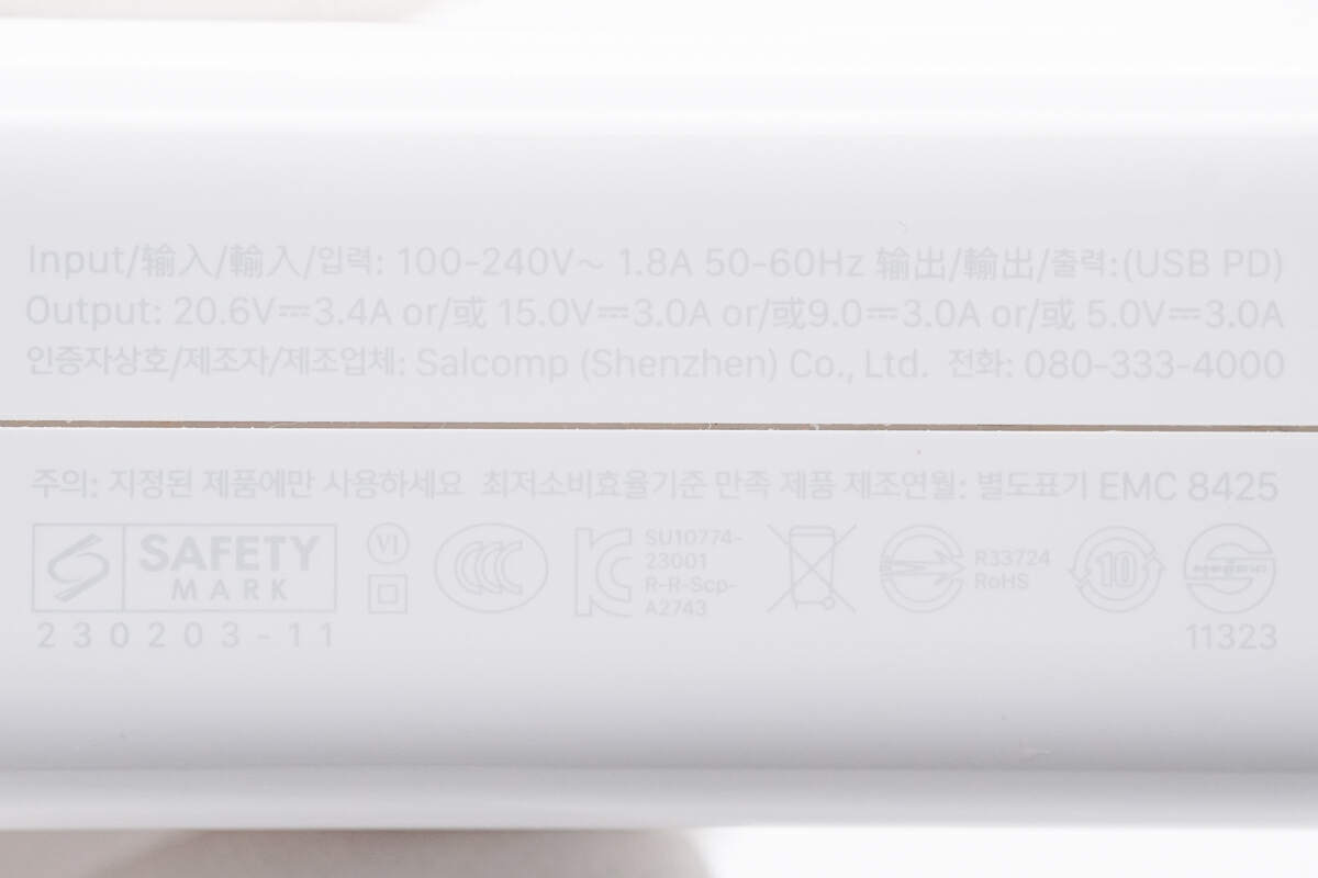
It supports input of 100-240V~50/60Hz 1.8A. The maximum output voltage and current are 20.6V and 3.4A, exactly 70W, and the manufacturer is Salcomp.
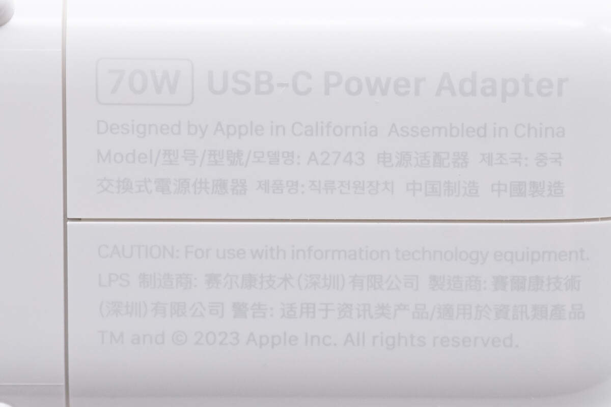
The model is printed on the other side, which is A2743.
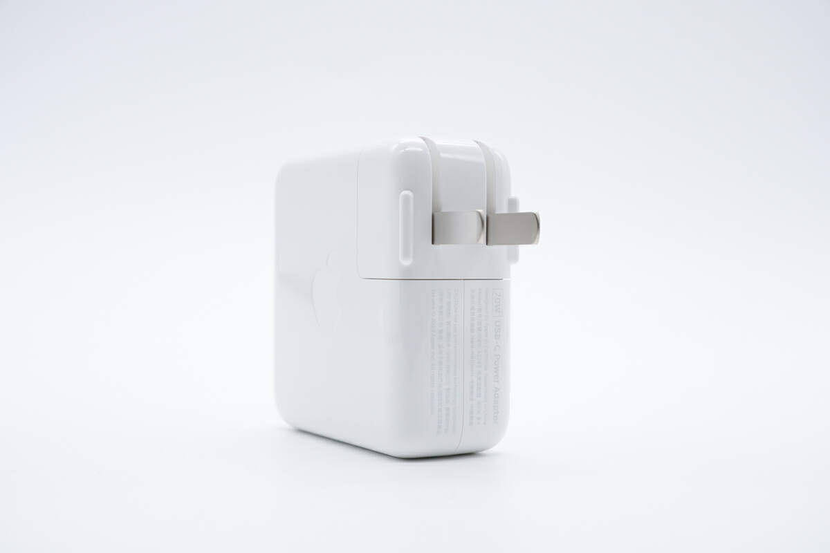
Like most Apple chargers, it also has a foldable input plug.
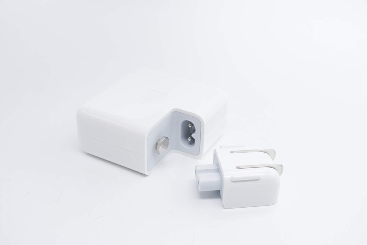
You can replace different plugs from different countries for traveling around.
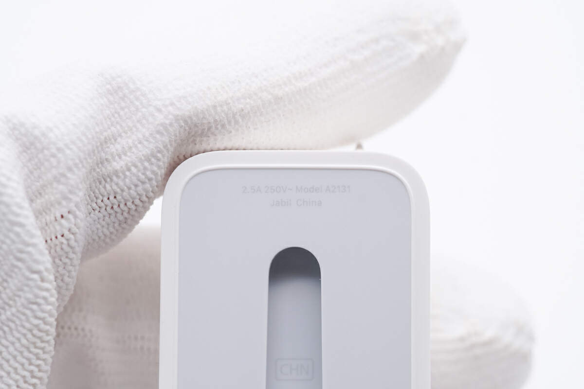
Surprisely, the included plug also has a model, which is A2131.
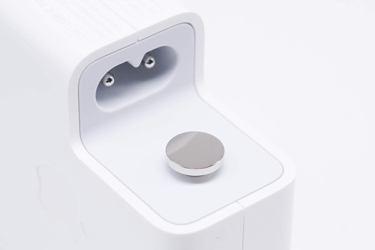
This round metal block is used for grounding and fixing.
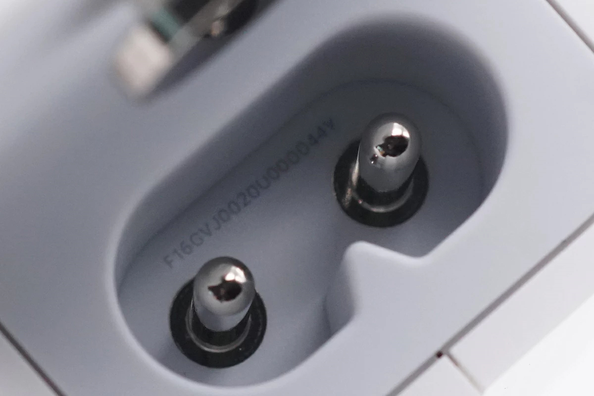
The slot is imprinted with an SN code, which is F16GVJ0020U000044Y.
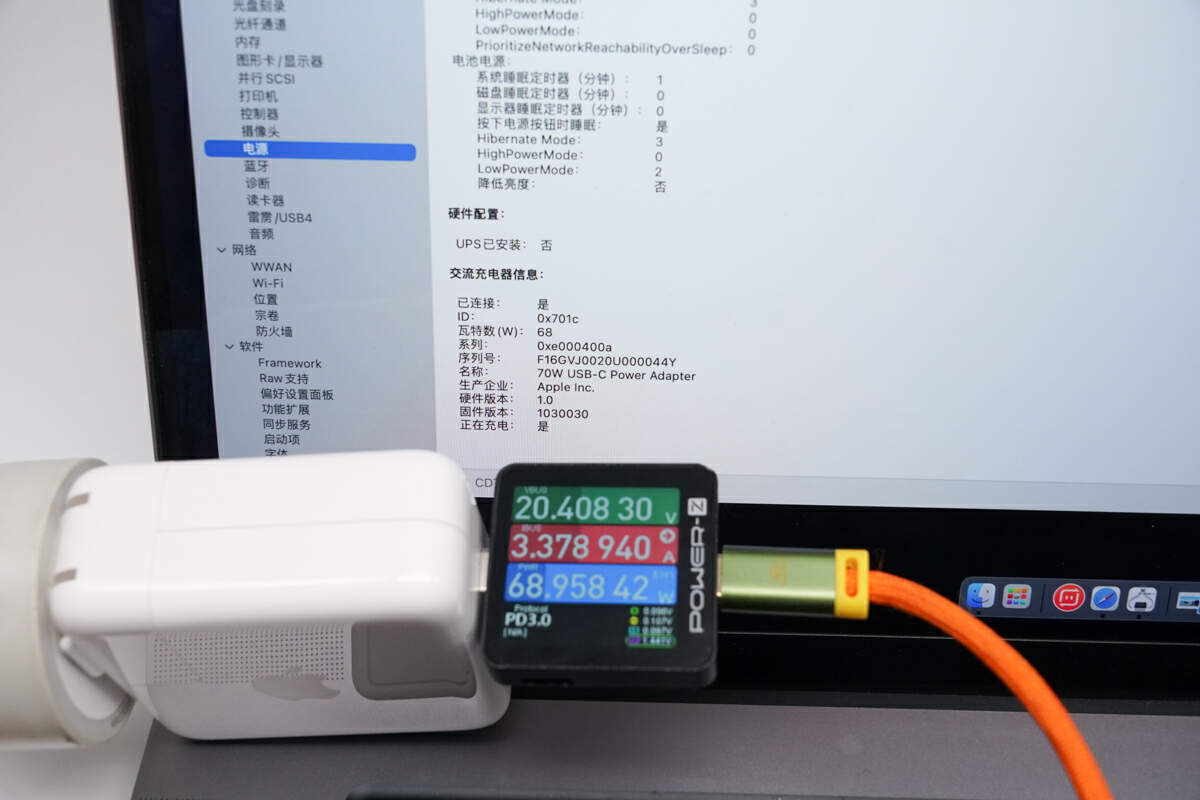
Connect the charger to the MacBook Pro, and the obtained serial number match the one mentioned above.
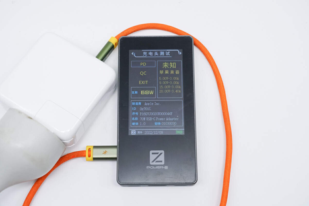
Furthermore, using ChargerLAB POWER-Z MF001 to read the SN code yields the same result.
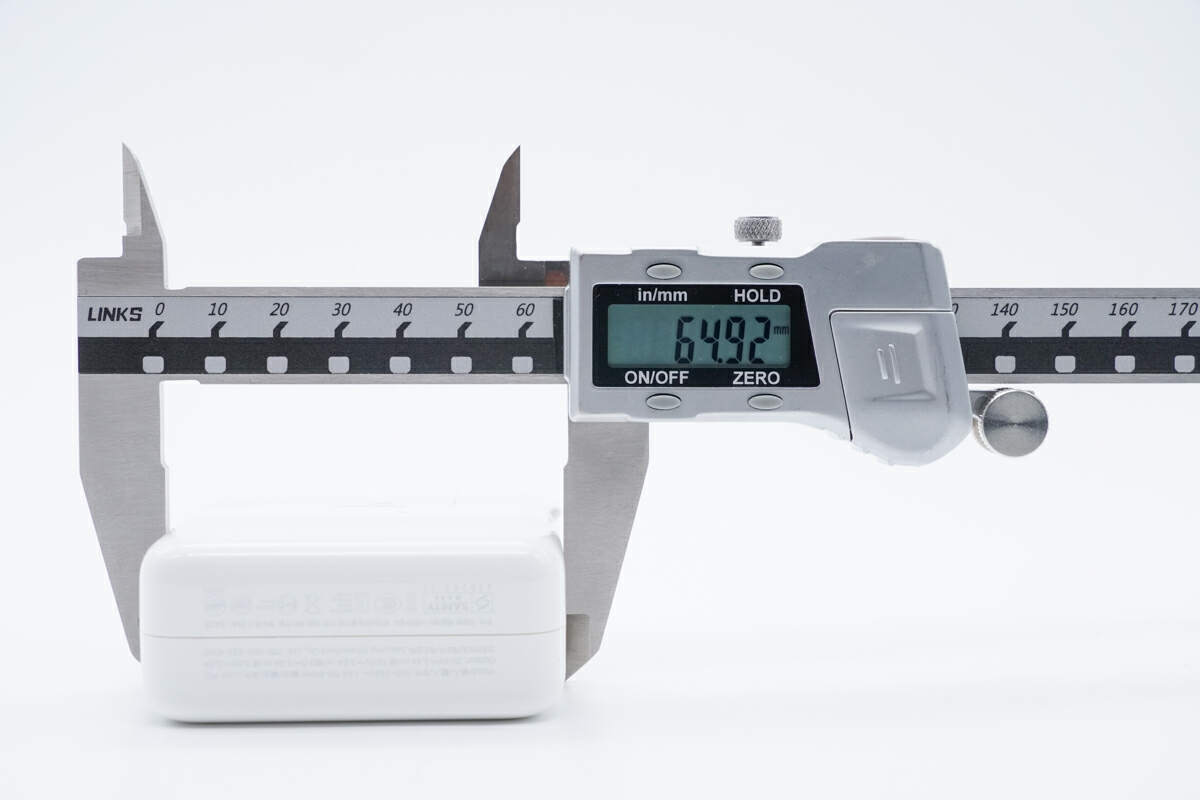
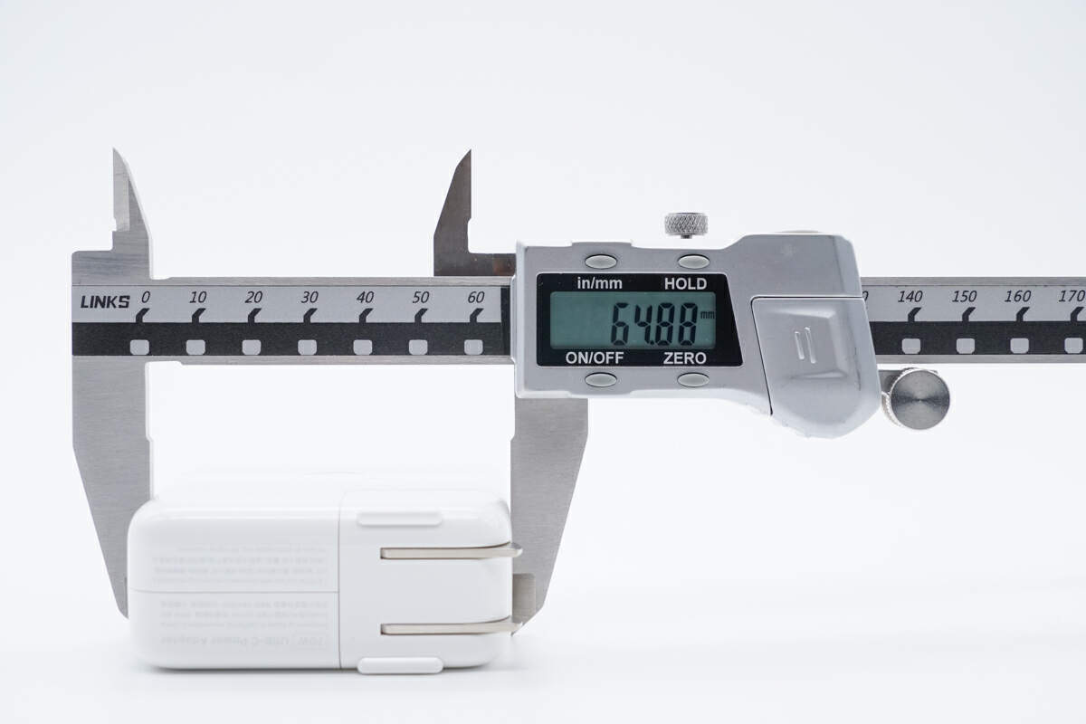
The length of this charger is about 65mm (2.56 inches).
The width is also about 65mm (2.56 inches).
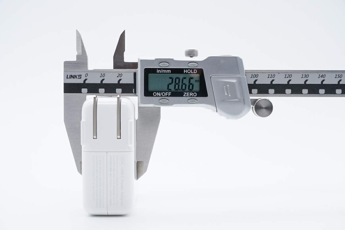
And the height is 28.5mm (1.12 inches),
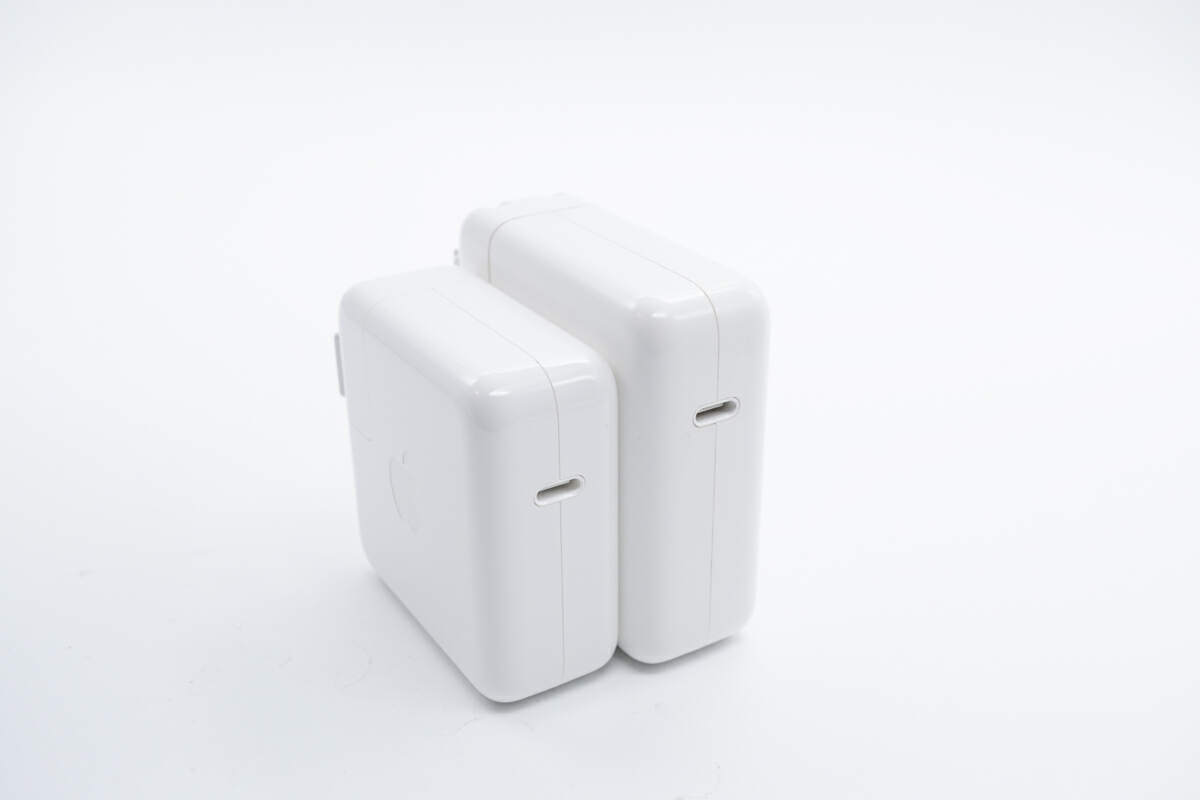
Due to the GaN components, it’s slightly smaller than the previous 67W.
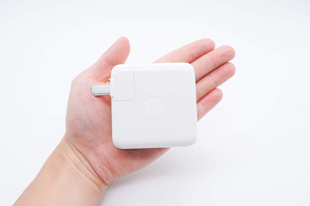
This is how it looks like on my hand.
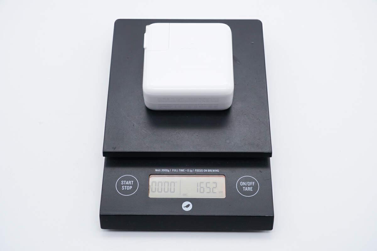
And the weight is about 165g (5.82 oz).
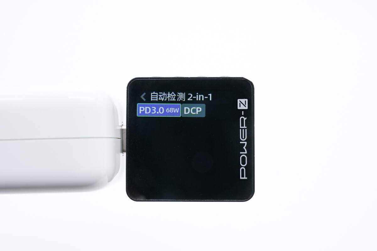
The ChargerLAB POWER-Z KM003C shows it only supports PD3.0 and DCP protocols.
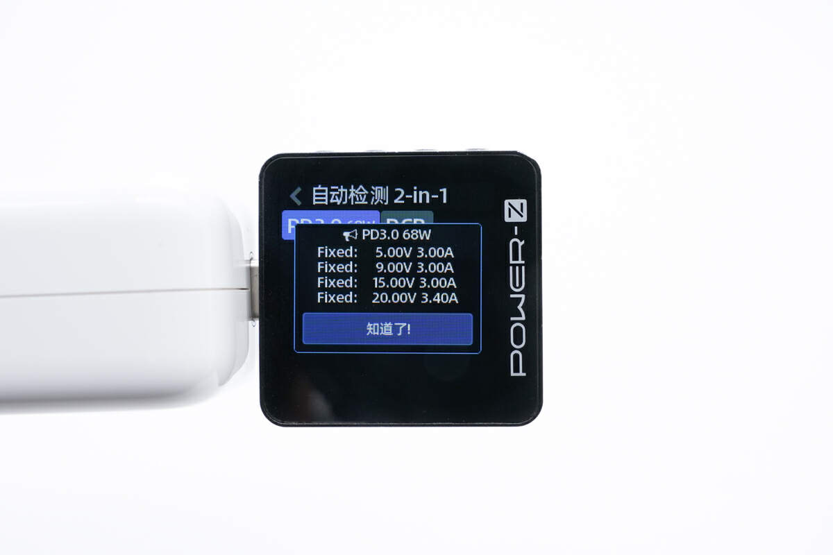
And it has four fixed PDOs of 5V/9V/15V 3A, 20V 3.4A.
The 20.6V is not the standard voltage of PD protocol, so it just shows 20V.
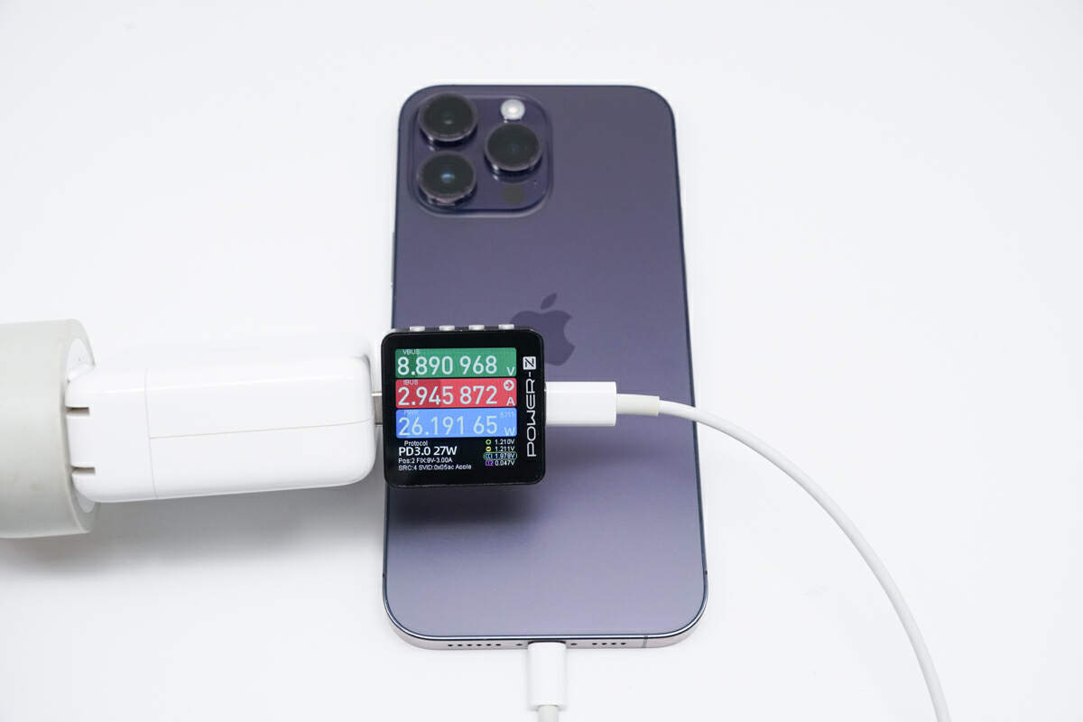
Use it to charge the iPhone 14 Pro MAX, the power is 26W.
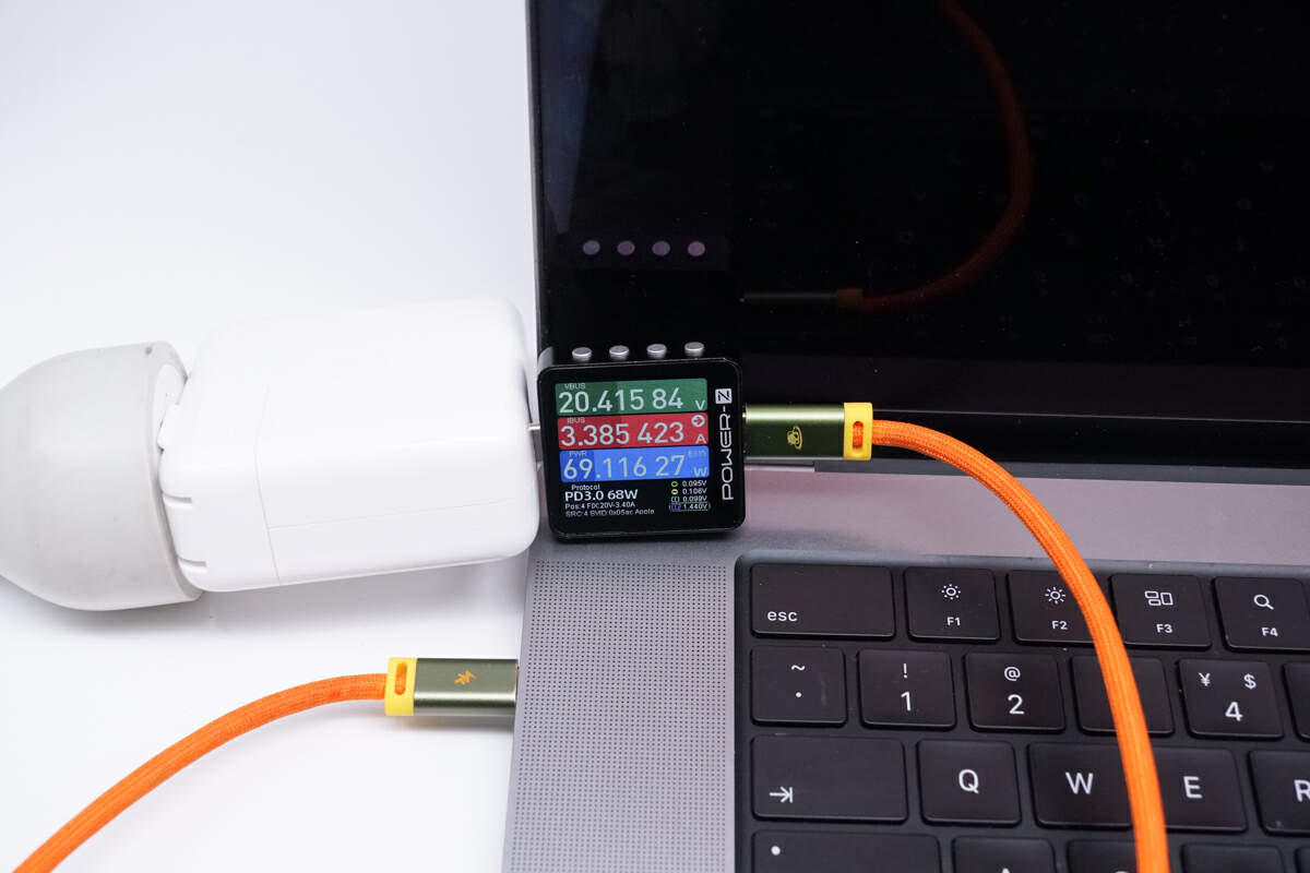
Then, for the 16-inch MacBook Pro M1 Max, it reaches an impressive 69.12W, with zero false advertising.
Teardown
Now that we have completed our unboxing and testing of this charger, it's time to take apart the device and examine its internal components and structure.
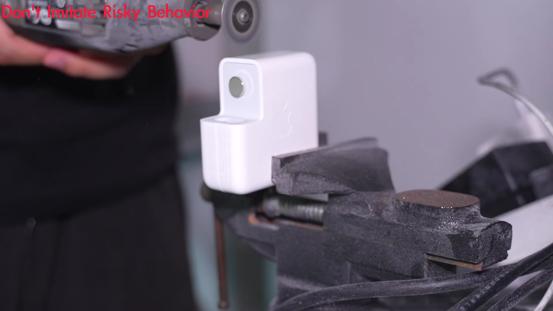
Next, let’s go ahead and use the cutting machine to destroy the outer case.

Use the spudger to separate those two parts.
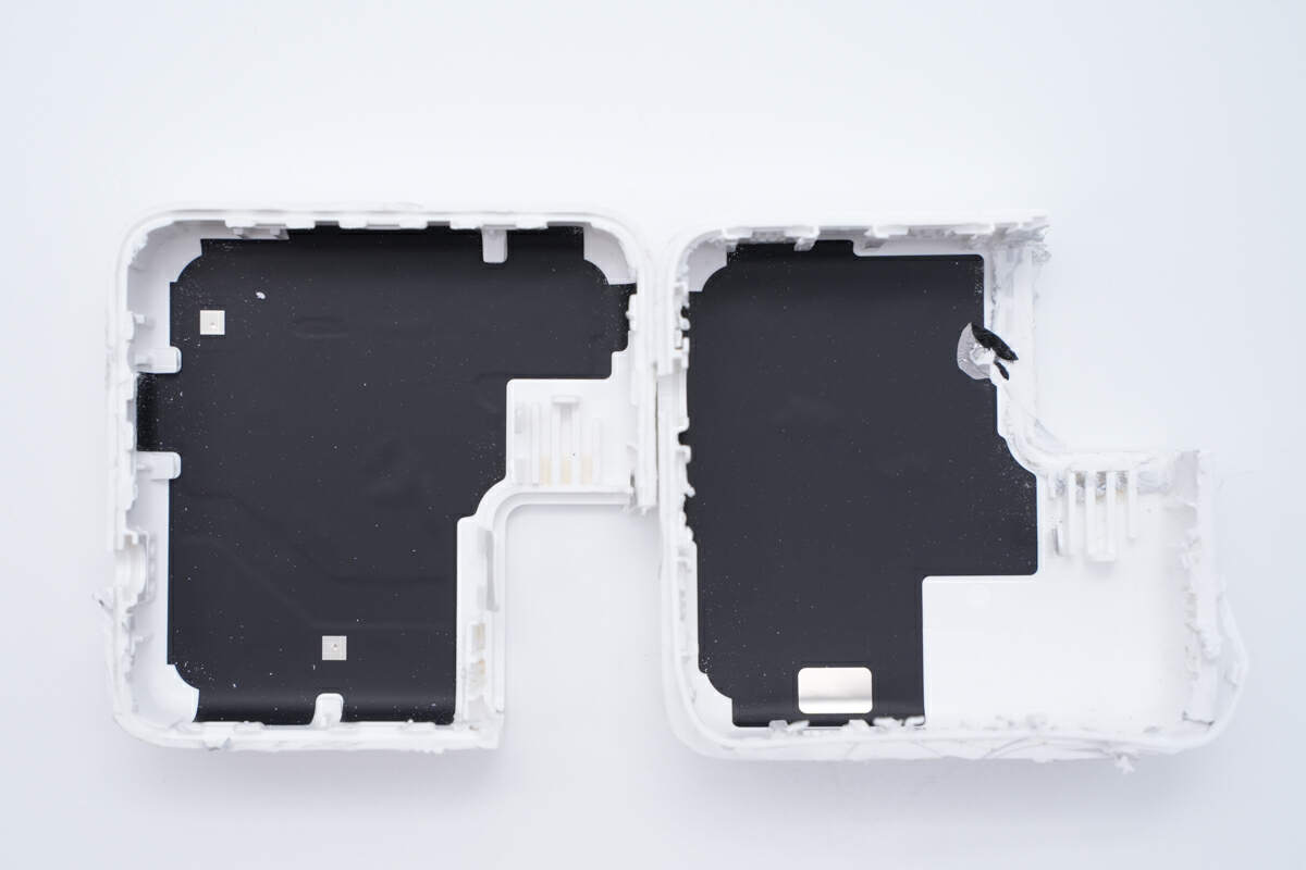
The black thermal graphite sheet is pasted inside the case.
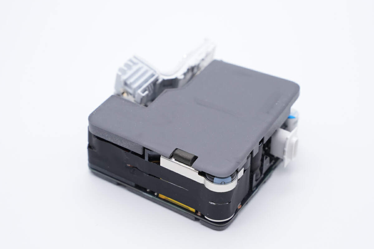
The front side of the PCBA module is covered with silicone pad for heat dissipation and buffering.
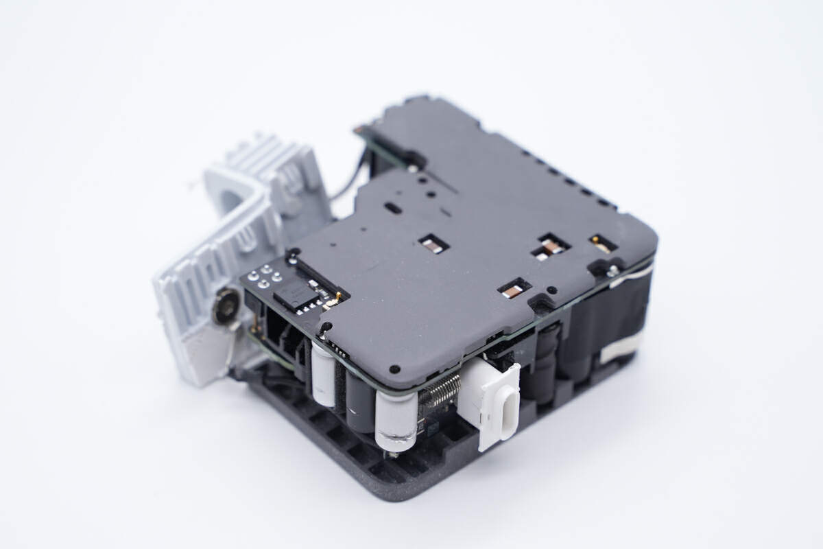
So is the back.
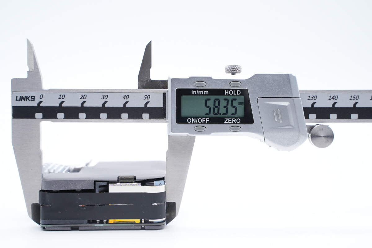
The length of the PCBA is about 58.5mm (2.30 inches).
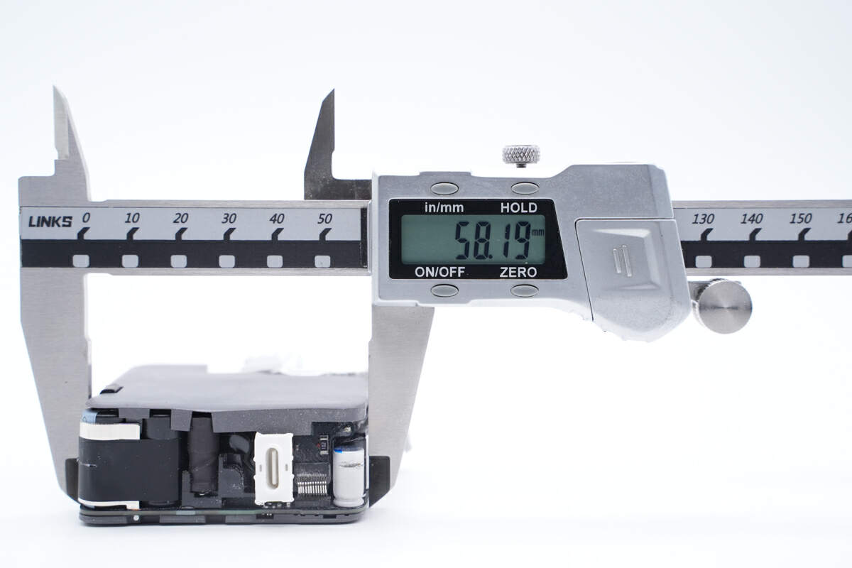
The width is about 58mm (2.28 inches).
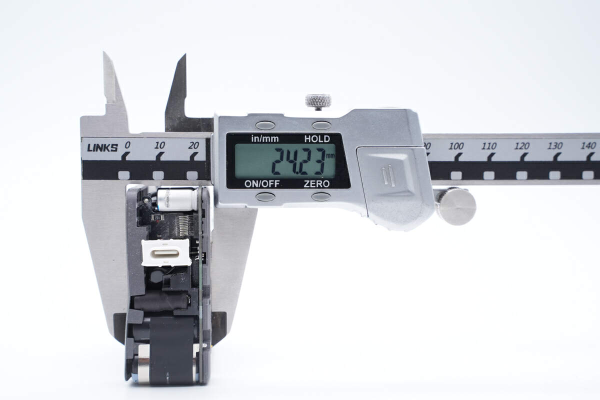
And the height is about 24mm (0.94 inches).
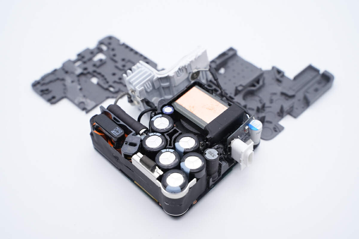
Take off the two silicone pads, you can clearly see that the gaps on them fit perfectly with the various components on the PCB, a very rare and thoughtful design.

The input plug is connected to the PCBA module through black and grey wires, and the solder joints are insulated with heat-shrinkable tubing.
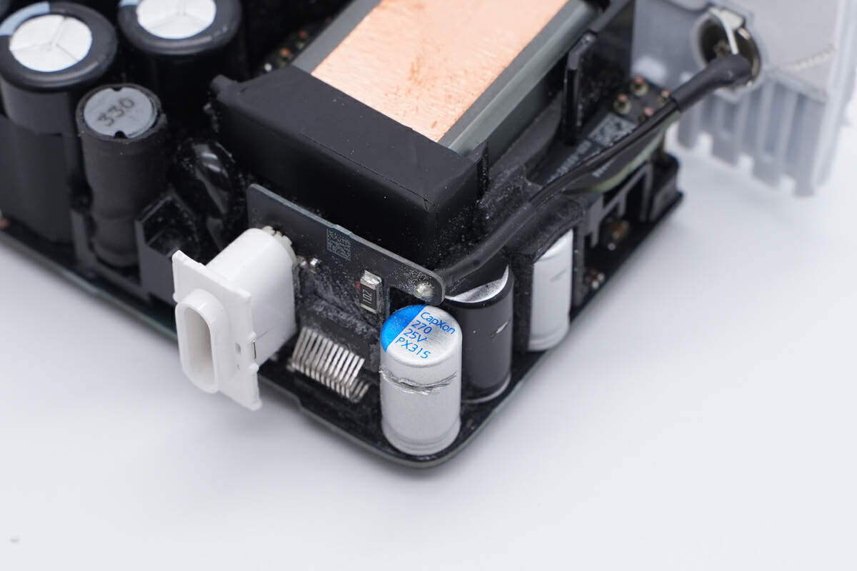
The ground wire is directly connected to the round metal block.
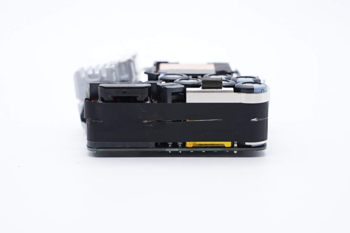
The black tape is pasted on the side of the PCBA module for insulation.

Disconnect the input plug from the module.
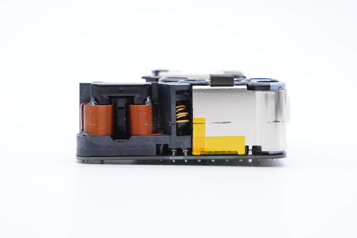
And tear off the black tape, a metal heat sink is wrapped on the right side.
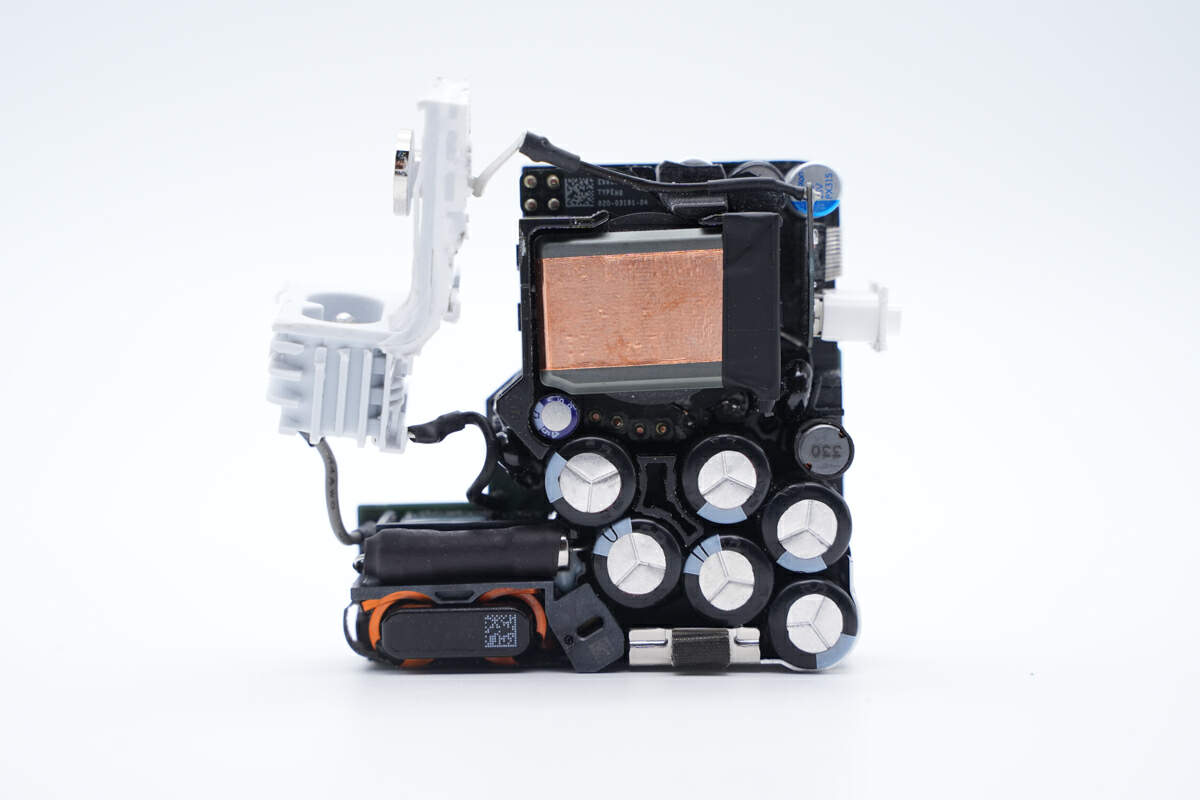
The fuse, common mode choke, transformer, and all capacitors are on the front.
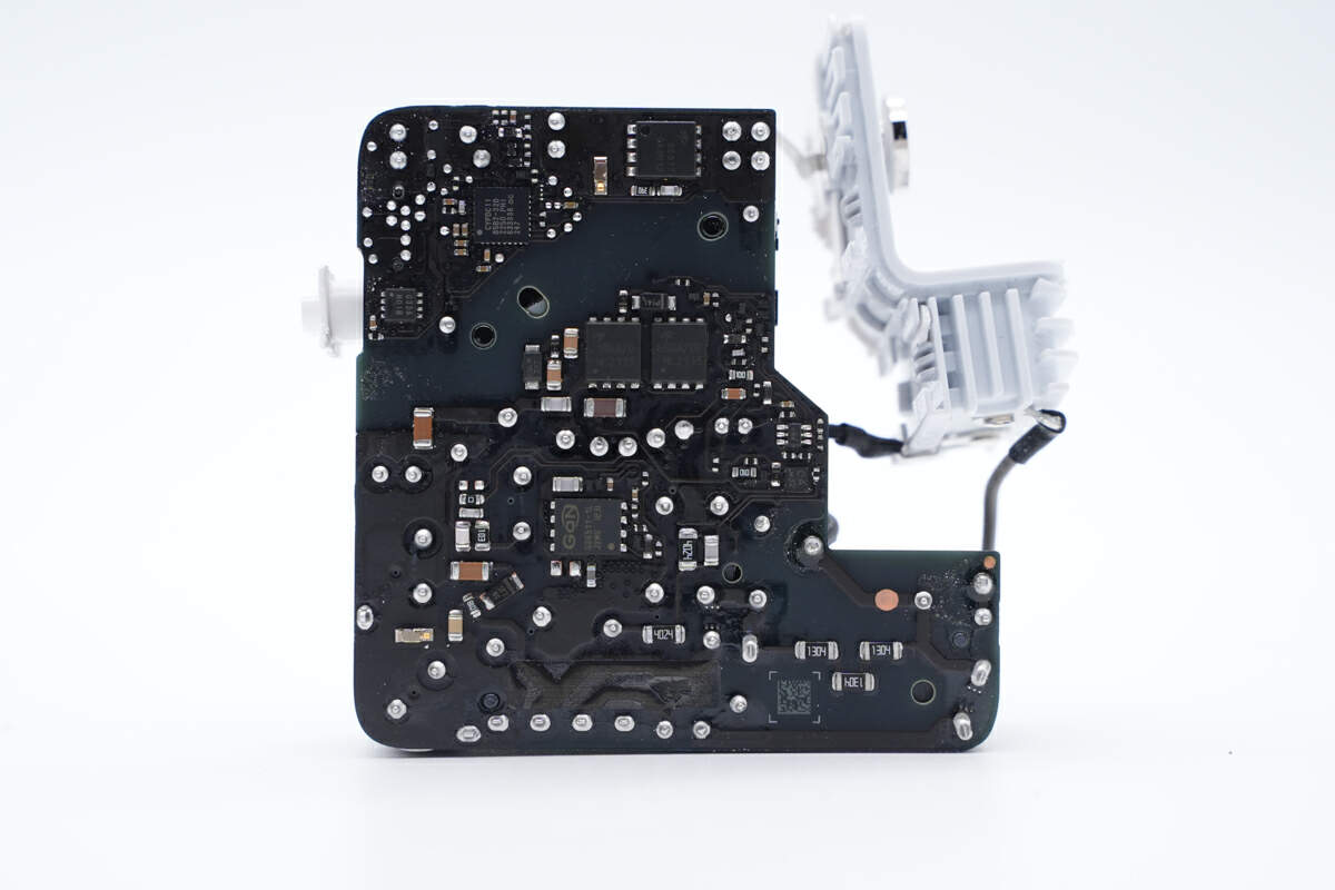
This is Apple’s second GaN charger with a GaN FET on the back.
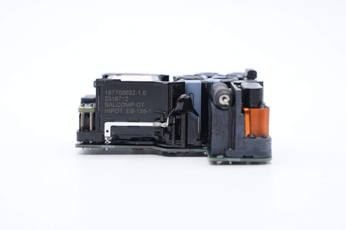
Then, let’s introduce all components one by one, starting from the input end.
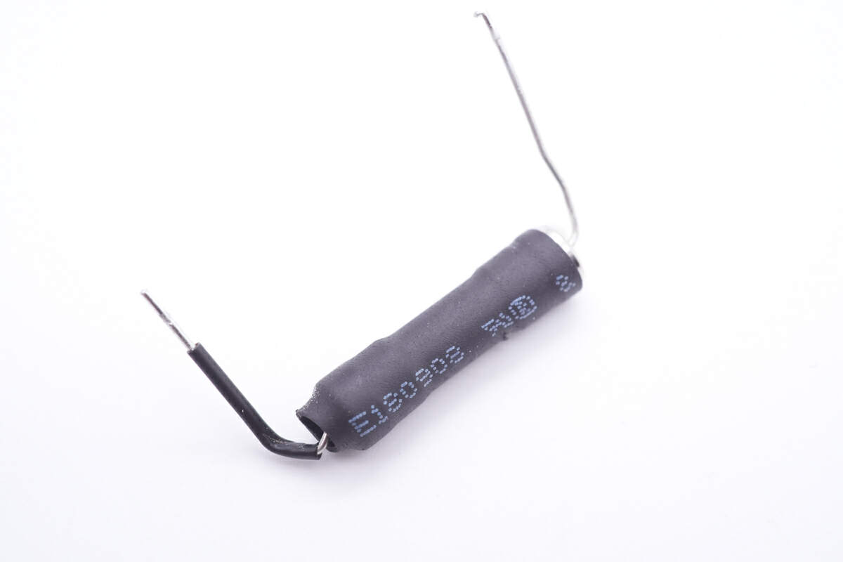
The input fuse is insulated with heat-shrinkable tubing.
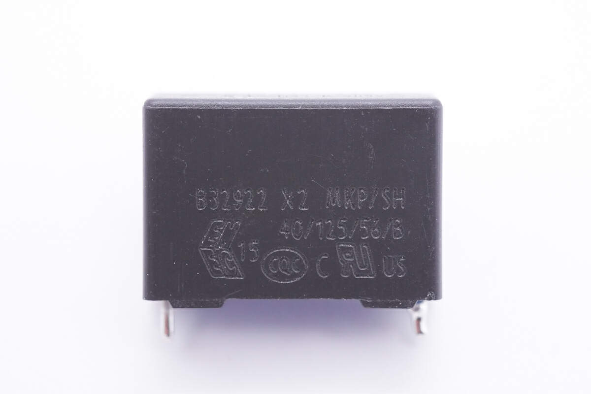
The safety X2 capacitor is from TDK. 0.22μF.
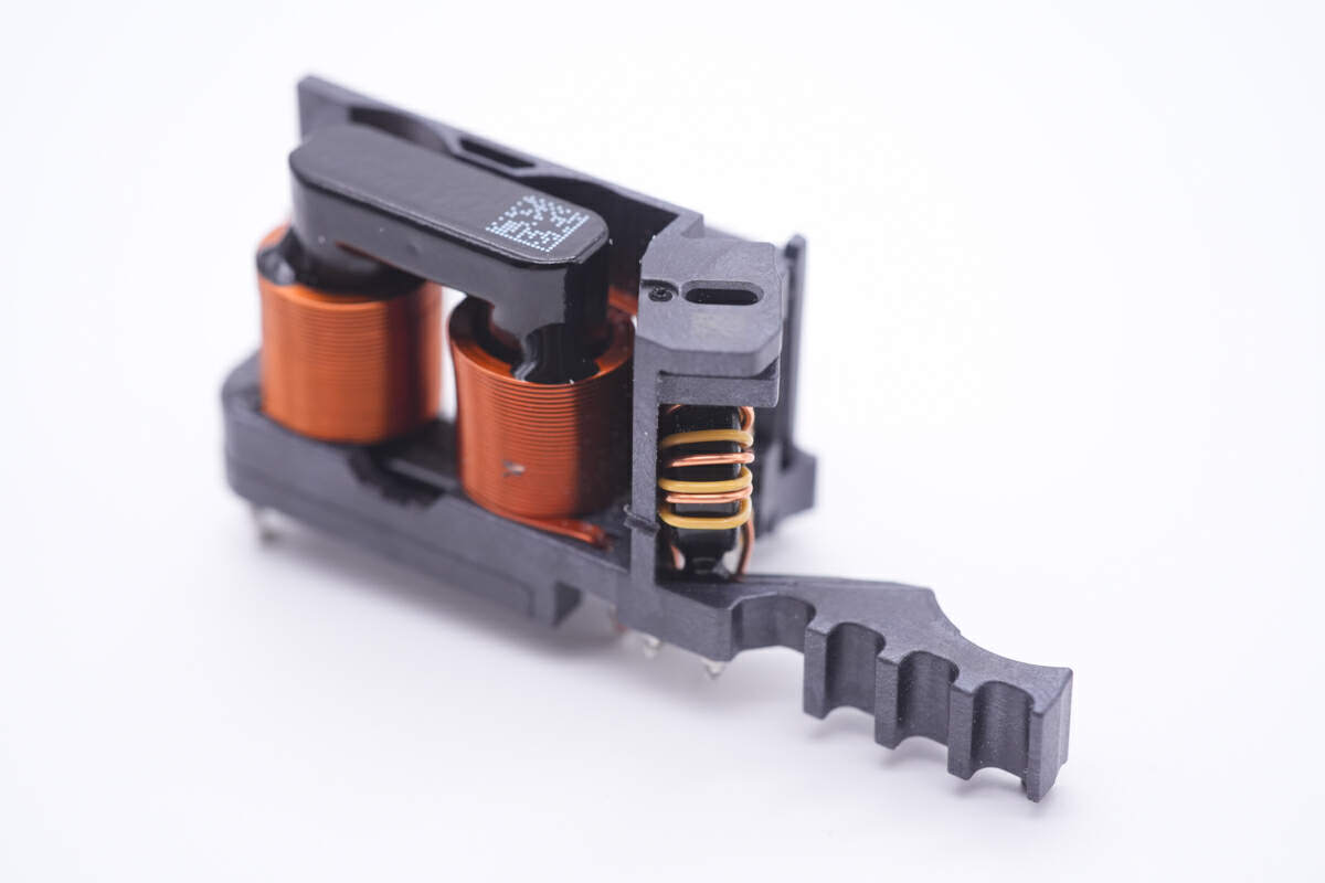
Two common mode chokes are fixed on an insulating frame.
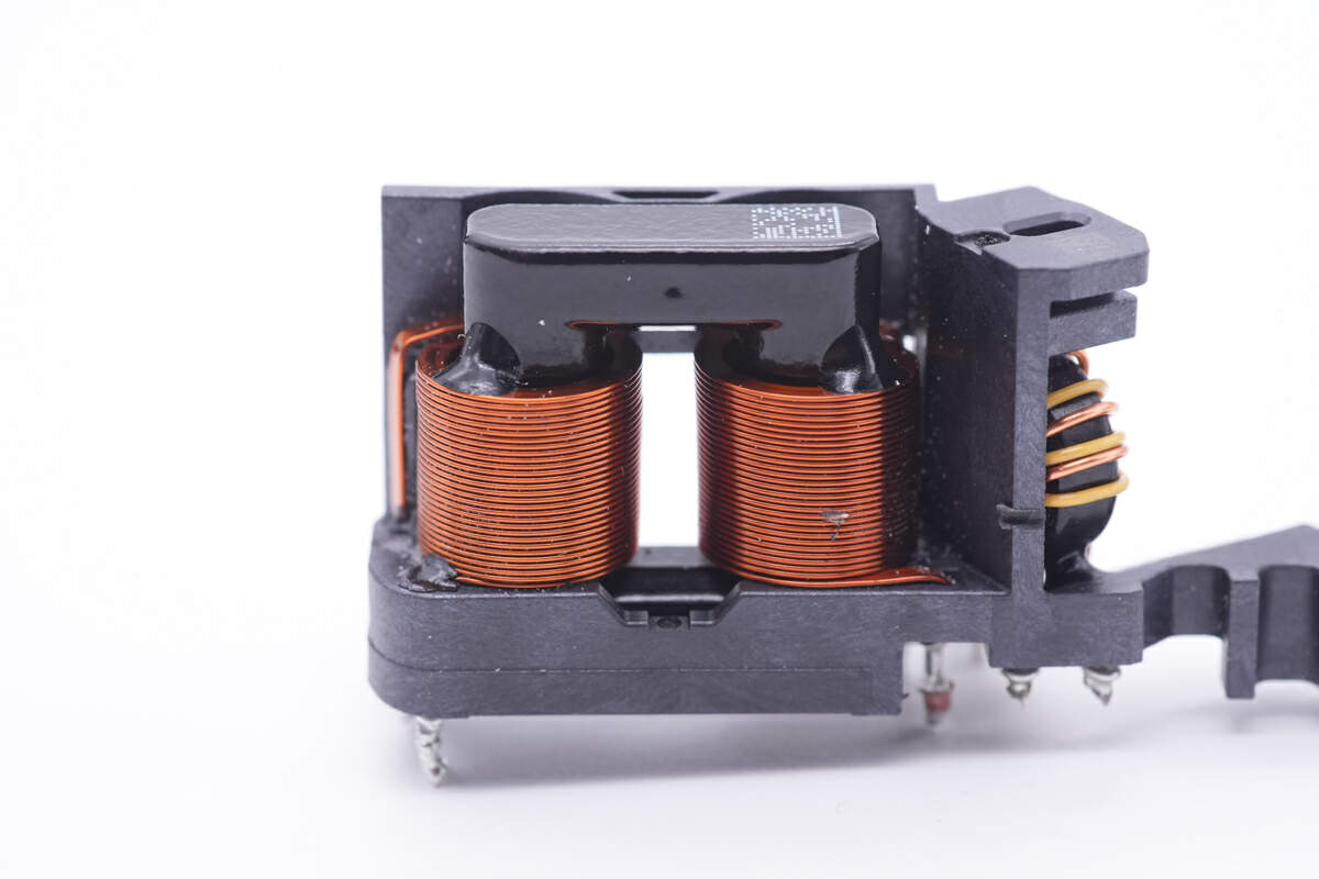
The first one is wound with flat copper wires.
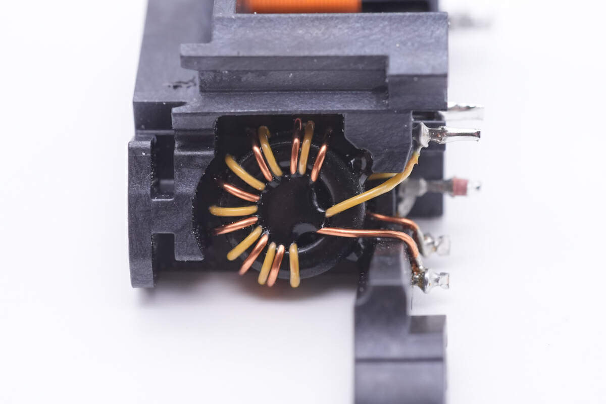
And the second one is actually smaller and is a toroidal-core inductor.
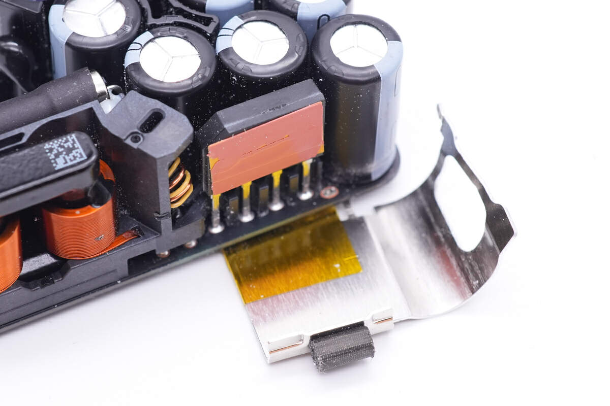
The bridge rectifier is under this heat sink to dissipate heat quickly.
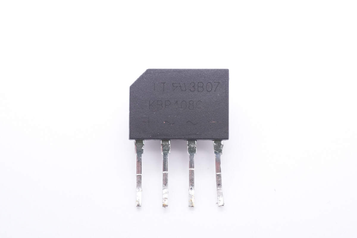
Model is KBP408G. 800V 4A.
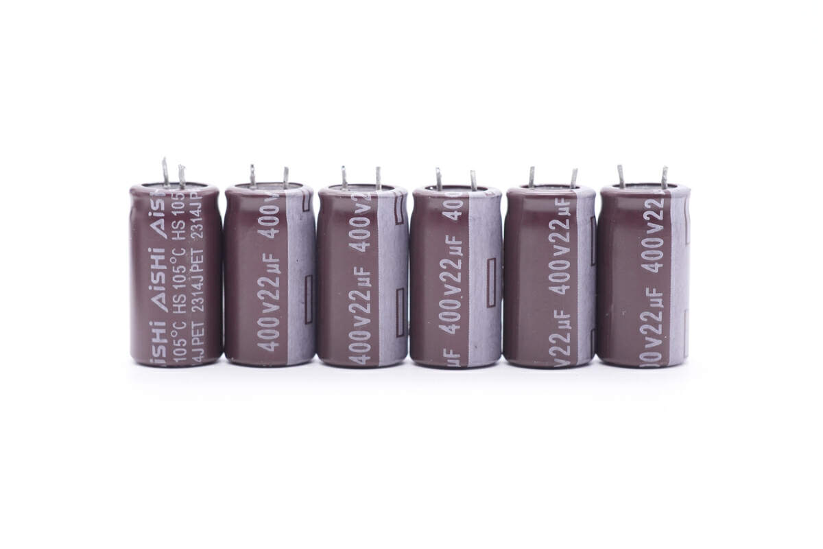
Those six electrolytic capacitors for input filtering are from AiSHi. They’re connected in parallel and 400V 22μF for each. 132μF in total.
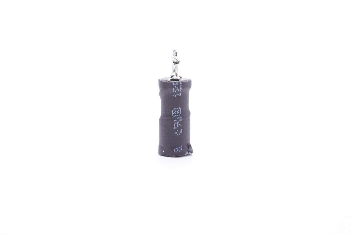
Here is the differential mode choke, insulated with heat-shrinkable tubing.
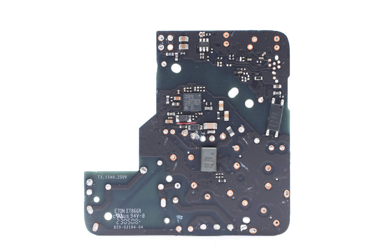
After removing all plug-in components on the front, we can find some chips under them.
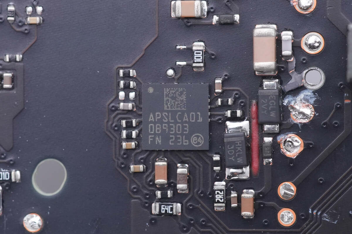
The master control chip is customized by Apple and marked with APSLCA01. We have seen this chip in many Apple original chargers.
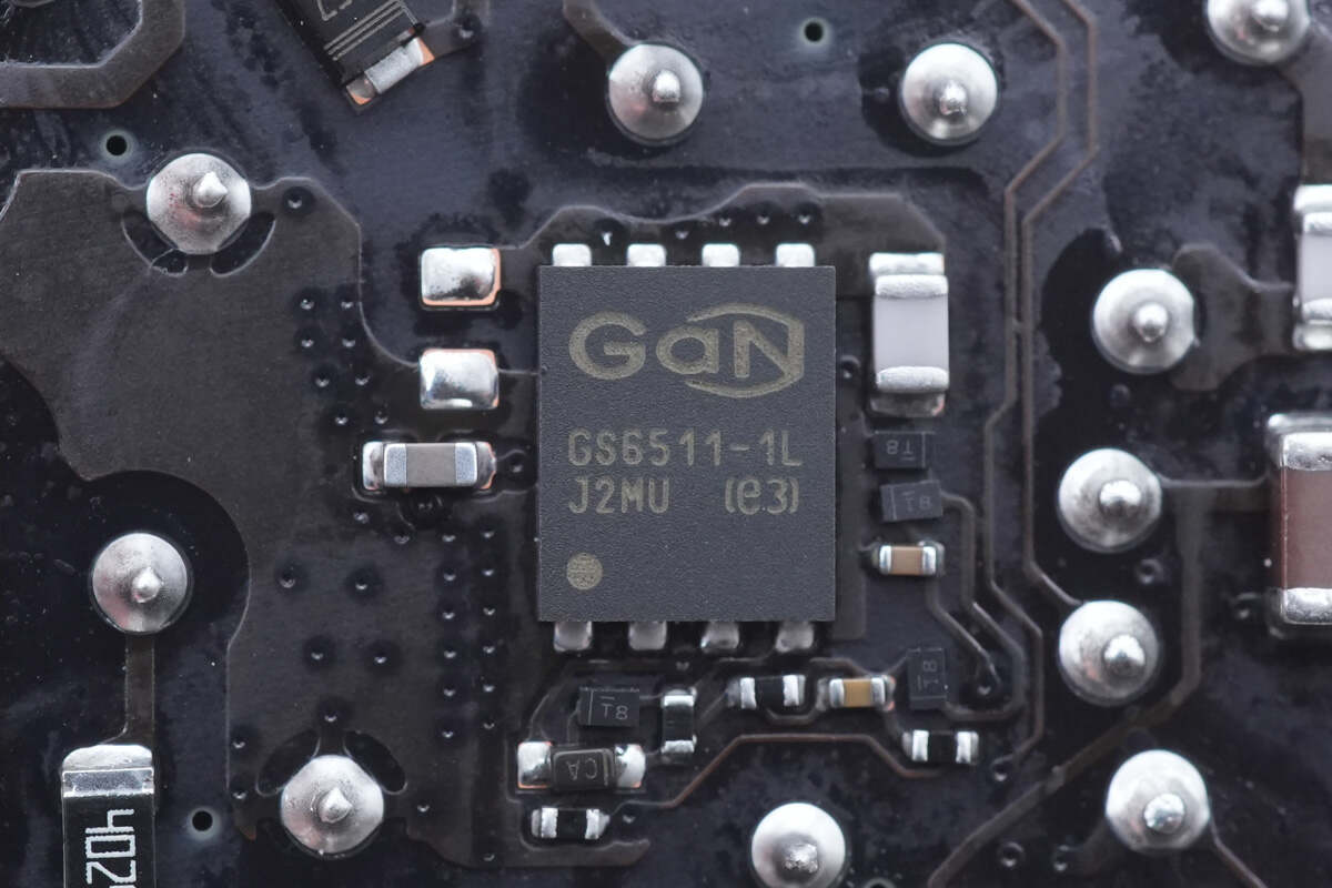
This is a GaN FET from GaN Systems. It adopts DFN5 x 6 package and is the same model as the Apple 140W. 650V, 150mΩ. Model is GS-065-011-1-L.
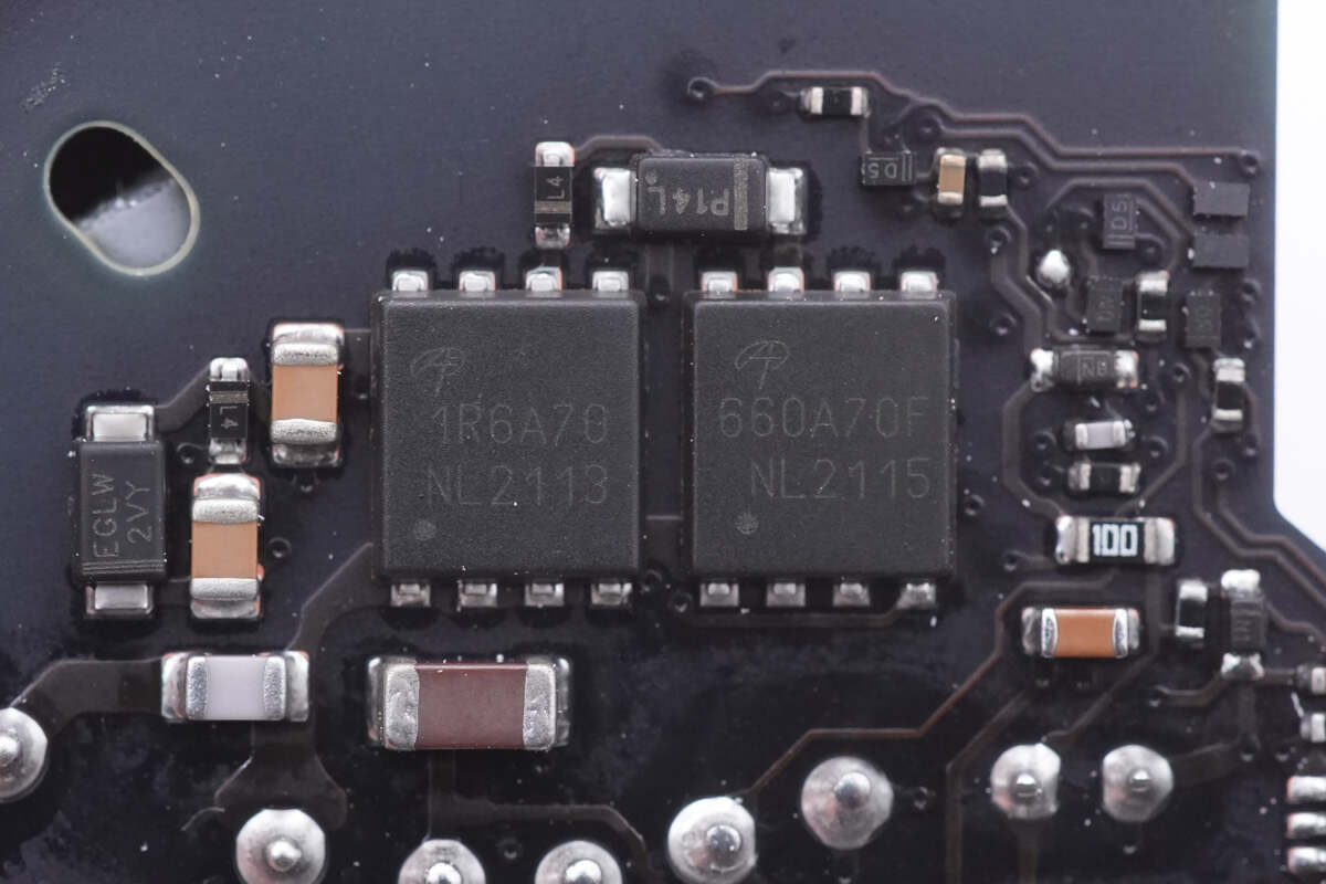
The other two MOSFETs are from AOS and adopt DFN5 x 6F package, but they have different models. The left one is AONS1R6A70. 800V, 1.3Ω. And the right one is AONS660A70F. 800V, 550mΩ.
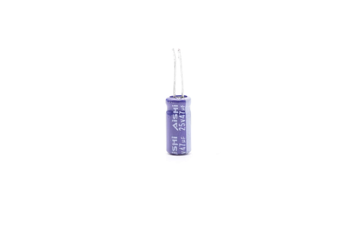
This electrolytic capacitor powers the master control chip. It’s from AiSHi and is 25V 47μF.
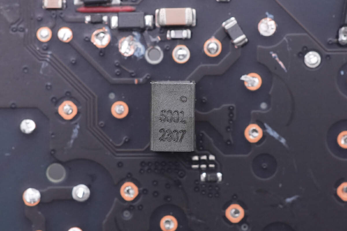
The SMD current transformer is used to detect the current of the primary side for over-current protection.
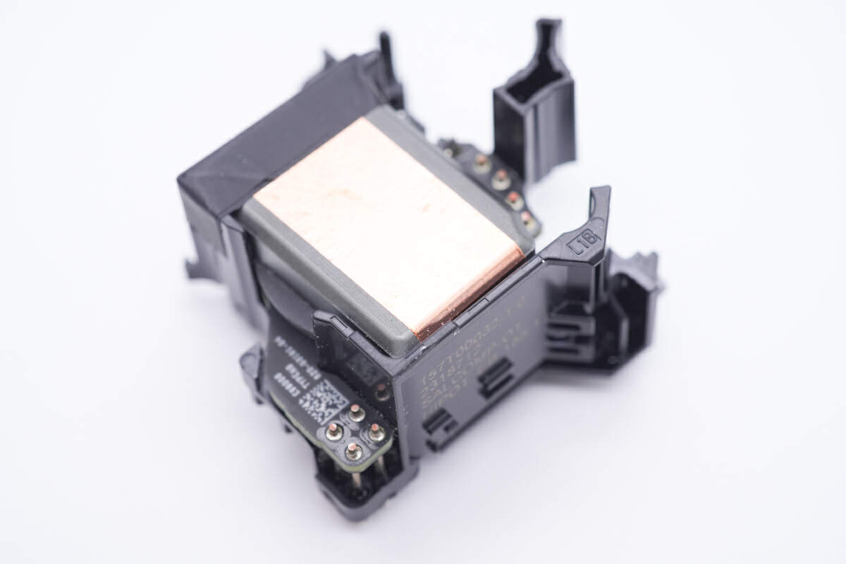
The magnetic core of the planar transformer is insulated by a plastic case.
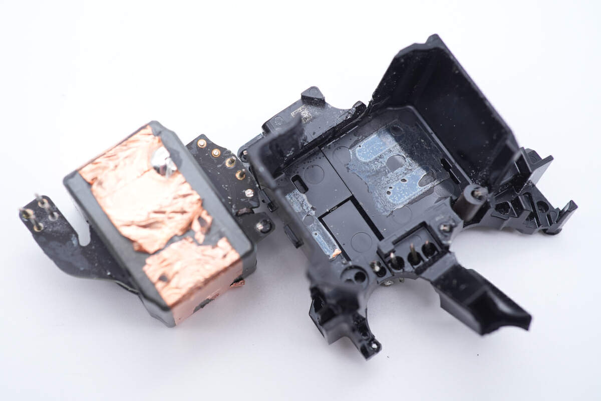
Take it out, the magnetic core is insulated by copper foil.
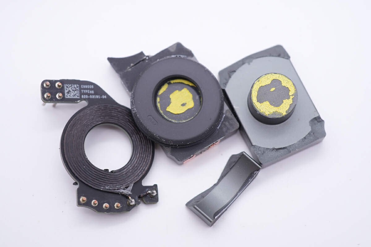
Going further and smashing it open, there are rubber pads attached to both sides of the internal PCB.
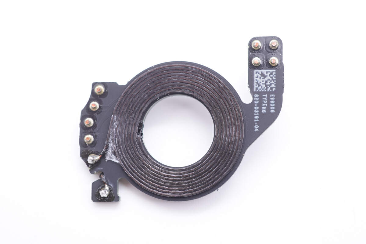
The coils are wound with Litz wire.
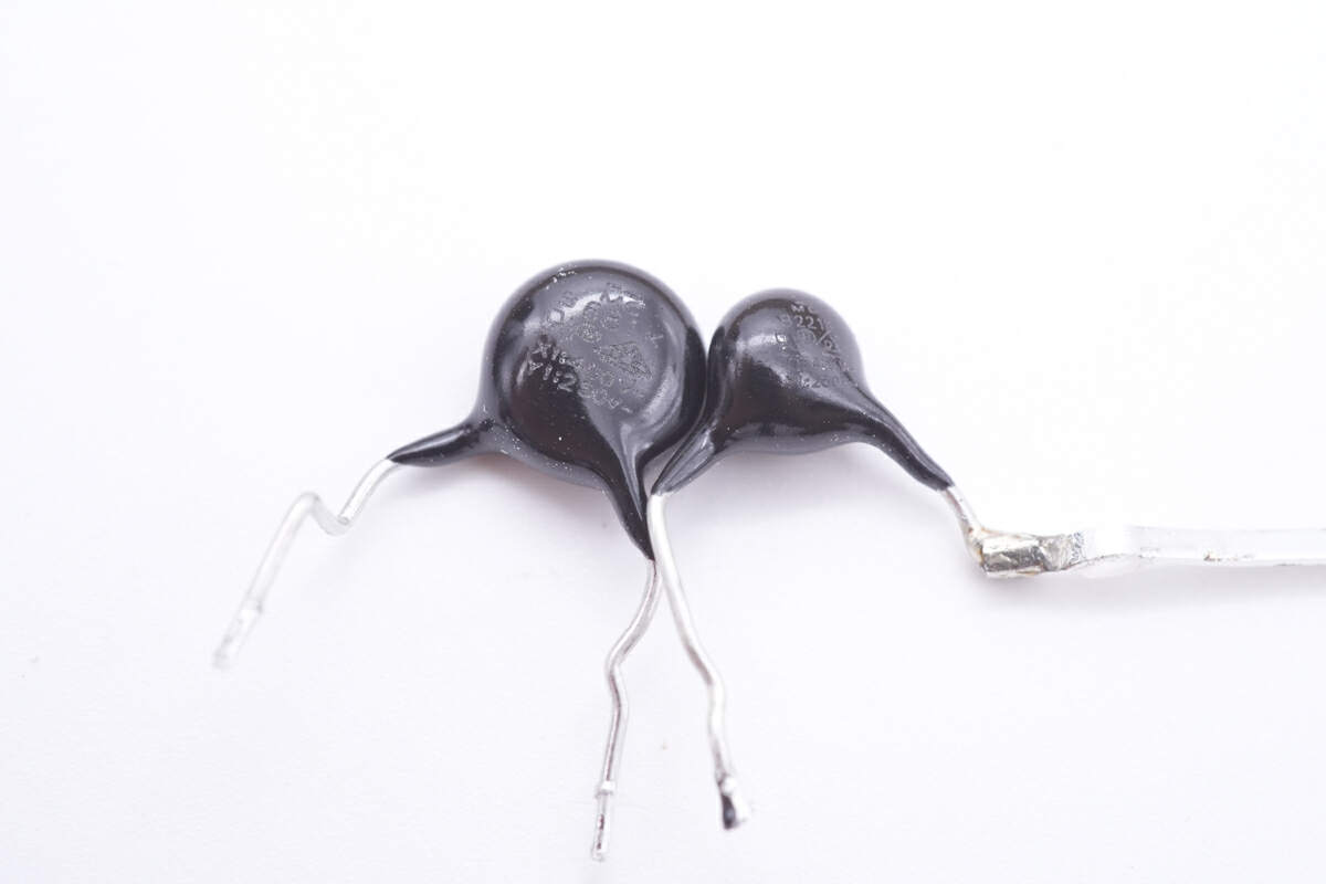
Two black Y capacitors are soldered on both sides of the transformer.
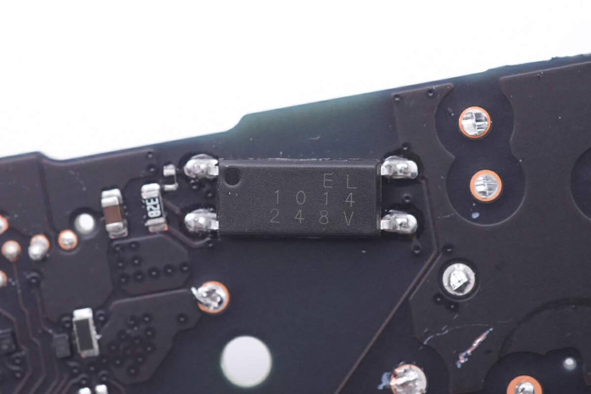
The EL1014 optocoupler is used to regulate the output voltage.
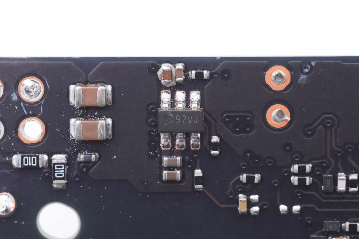
Then, let’s move to the synchronous rectification circuit. Its controller is marked with D92vJ.
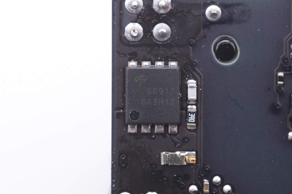
And the synchronous rectifier is from AOS and adopts DFN5 x 6 package. 100V, 2.9mΩ. Model is AONS66917.
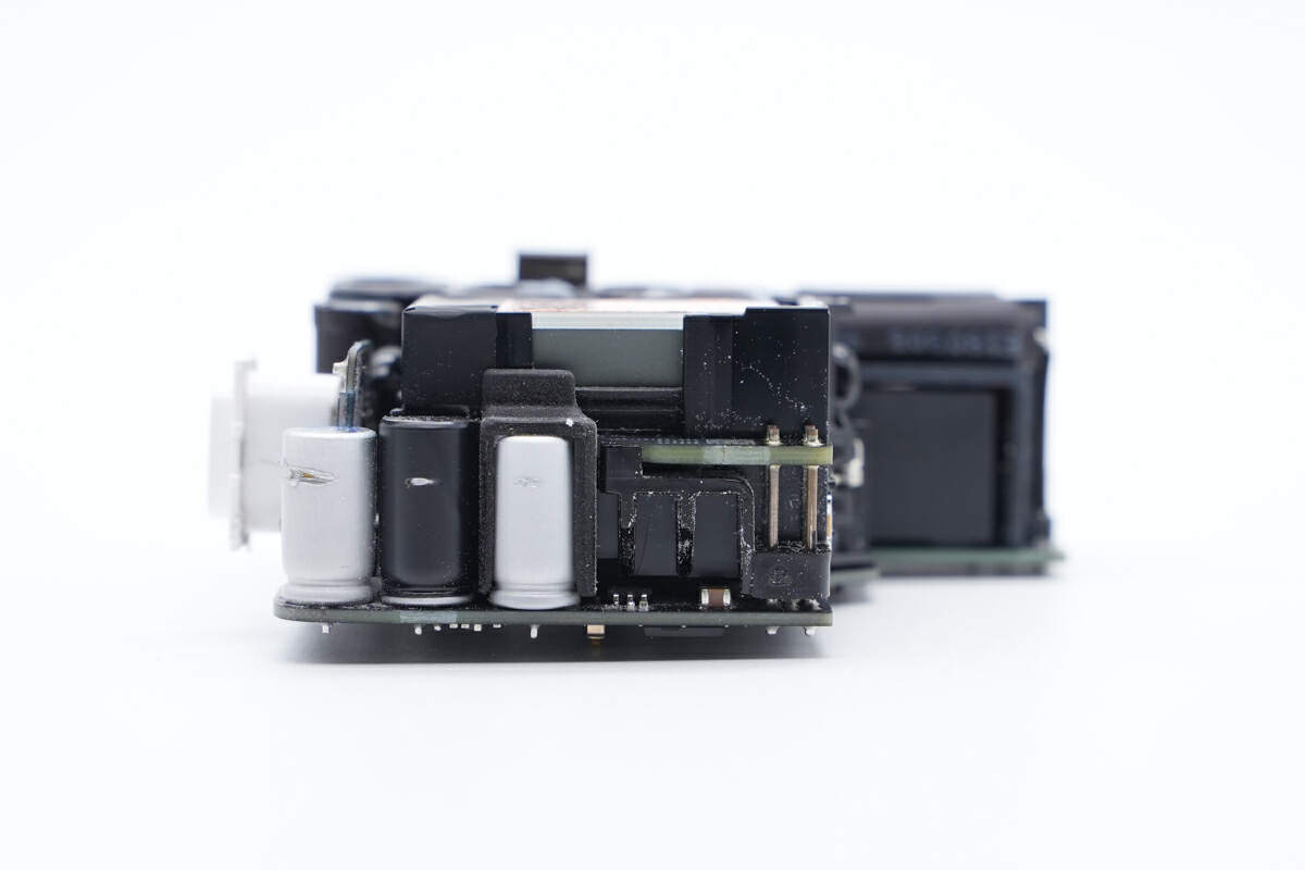
As for the output end, there’re three solid capacitors for output filtering.
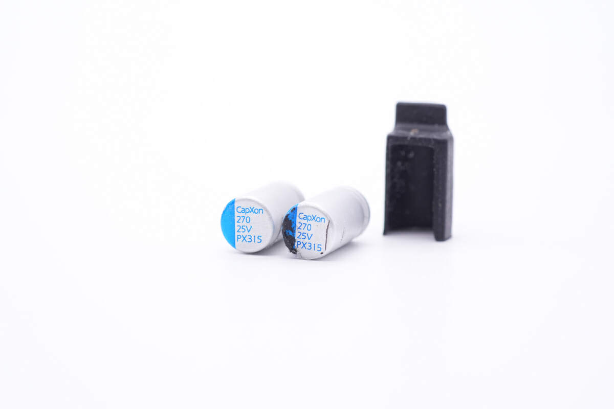
Two of them are from CapXon PX series. 270μF 25V for each.
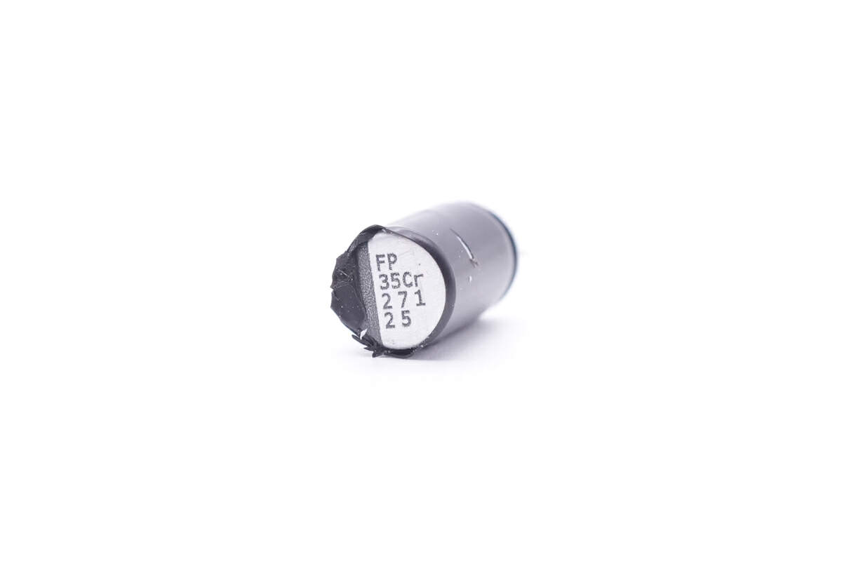
The black one is from Nichicon. It’s also 270μF 25V, but is wrapped with tape for insulation.
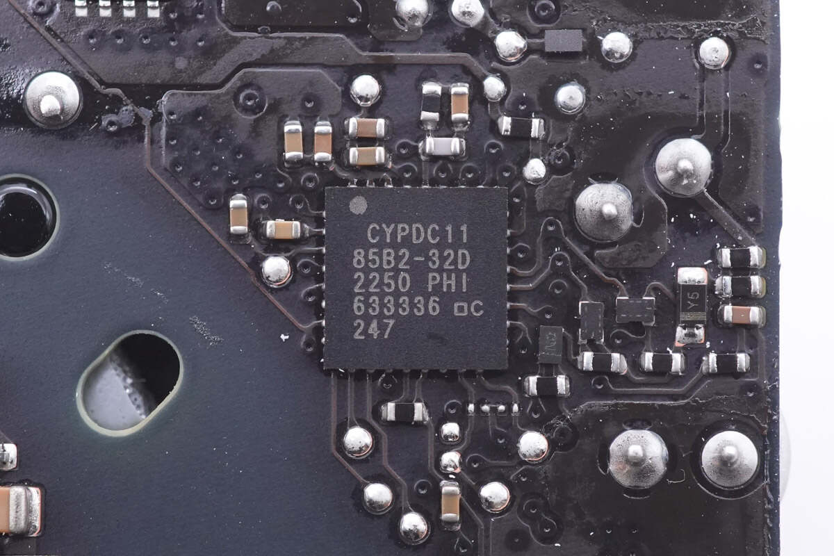
The protocol chip is from Infineon CCG3PA2 series.
It integrates a 32-bit M0 processor and has multiple protection functions. Model is CYPDC1185B2-32D.
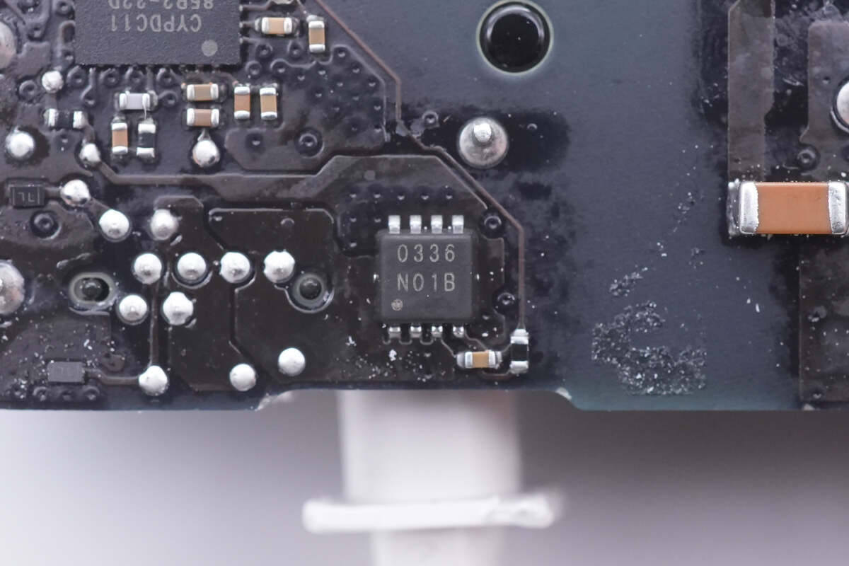
This is the output VBUS MOSFET, marked with 0336.
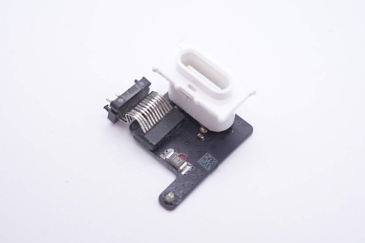
The USB-C connector is connected to the main PCB.
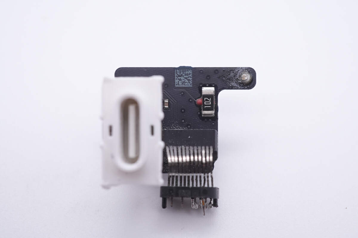
And there is a 1KΩ resistor next to it.
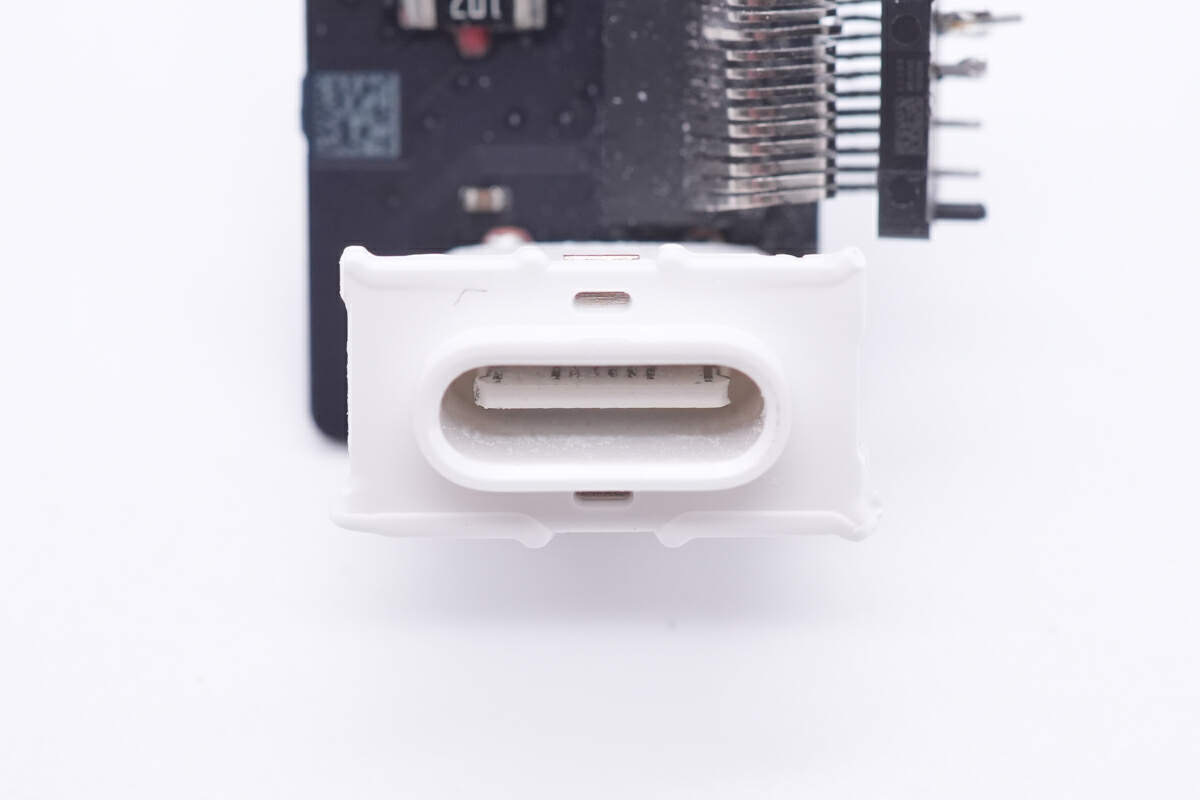
The plastic sheet inside the USB-C sockets is white.
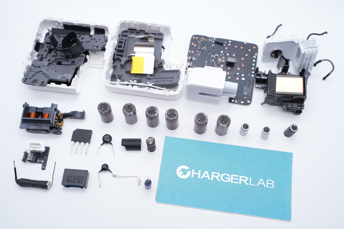
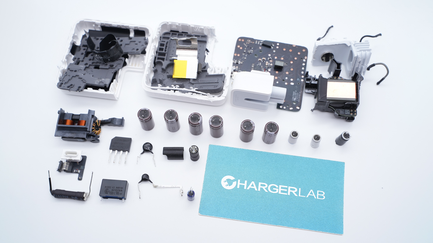
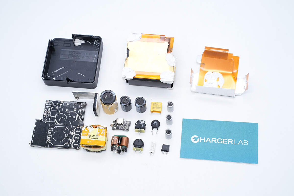
One last look at all the components of this AOHi Magcube 140W GaN Charger.
Summary of ChargerLAB
Well, as Apple’s second GaN charger, it’s smaller than the previous 67W charger but with higher output power. This technological advancement allows users to enjoy faster and more efficient charging for their devices.
After taking it apart, we found that there was no PFC circuit, and the heat dissipation measures are pretty good. The internal design is very compact, and most components are black, which looks neat. Except for components from AOS, Nichicon, and Infineon, we also found components from new suppliers such as AiSHi and CapXon.
Related Articles:
1. Brand New Apple 70W GaN Charger - ChargerLAB Compatibility 100
2. Latest Teardown of Brand New Apple 140W USB-C GaN Charger
3. Teardown of Brand New Apple 70W GaN USB-C Power Adapter (Video)

