On october 19, 2021, Apple held the special event, released AirPods 3, 2021 Macbook Pro, and also brought a new color for HomePod mini.

The brand new MacBook Pro 16 inch is equipped with powerful processors M1 MAX.
It supports up to 140W fast charging. And it’s also the world’s first laptop that supports USB PD3.1 protocol, which makes it can support up to 140W PD fast charging.

There is also a customized USB-C to MagSafe 3 cable.
You have to use this cable to achieve 140W charging.

Except for this 140W PD charger, Apple has released ten PD chargers, from 18W to 140W.
We made a chart for you to check out.

Many people are curious about the internal design, architecture of the first PD 3.1 GaN fast charger, and what kind of brand new components are inside.
We will test and teardown this charger to answer those questions.
1. Appearance of Apple 140W GaN Charger

Firstly, it continues the simple white shell of other Apple PD chargers and adopts the glossy surface, and the corners are rounded.

But compared to 81W, 87W and 96W, it changed from the traditional square to rectangle.

We can see Apple logo in here.

Model is A2452. And the manufacturer is Flextronics Power.

It supports input of 100-240V~50/60HZ 2A and output of 5V3A, 9V3A, 15V5A, 20.5V5A, 28V5A.

It is still equipped with foldable pins and a replaceable plug.
You can conveniently change the plug you want to use.

You can replace the plug equipped with ground wire.

It only has one USB-C.

Take a closer look at the USB-C.

The length of the charger is about 96mm (3.78 inches).

Width is 75mm (2.95 inches).

Thickness is 28mm (1.1 inches).

Here is how you hold it.

And the weight is about 277g (8.01 oz).

Use ChargerLAB POWER-Z KT002 to test the protocols.
It supports Apple 2.4A, Samsung 5V2A, DCP, PD3.0 protocol
And actually, PD3.1 is also supported.

And the supported five fixed PDOs are 5V3A, 9V3A, 15V3A, 20V4.7A, and the 28V 5A additionally.

Connect it to the outlet and use ChargerLAB Power-Z KM001C to test, we can see it can reach 27.73V 4.92A 136.68W.
2. Teardown of Apple 140W GaN Charger

Use the cutting machine to open the shell.

The shell is very thick.
And those black glue is used to fix the module.

This is the ground wire that is connected to the plug.

The solder joints of AC wire are insulated with heat-shrinkable tubes.

The large heat sink is covered on the PCB module.

It fixed with screws and used to evenly dissipate heat.

The insulating tape is pasted on the side.

The length of PCB module is 87.6mm (3.45 inches).

The width is 67.07mm (2.64 inches).

And the thickness is 23.2mm (0.91 inches).

Remove the heat sink, and we can see the internal module.

And the insulating plates are black.

The capacitors, inductors, and other components are on the front of the module.
And the transformer is covered with plastic.

Remove the plastic.

The back of the PCB is covered with a rubber pad for insulation and protection.

And the thermal adhesives and graphite thermal pads are on different chips.

We can see the electrolytic capacitor for high-voltage filtering, current transformers, film capacitors, capacitor for power supply, etc.
The electrolytic capacitor is placed horizontally and covered with insulating tube.

After removing all the plug-in components,
We can see four diodes, two drivers, optocoupler, protocol chip, and output VBUS switch MOSFET are on the front.

Flip to back, we can see PFC boost circuit, LLC switching power supply controller, and MOSFETs.

Here is the input end.
The safety X capacitor is covered with a plastic, and the fuse is equipped on the top.
There are two Infineon MOSFETs on the right.

The rated current of the fuse is 3.15A.

This is the safety X capacitor.

The common mode choke is used to filter out EMI interference.

Another common mode choke is winded by blue and black wires.

This varistor is used for input overvoltage protection.
Model is TVR10621M.

Those four diodes at the input can form the full-bridge rectifier.

Those two diodes can cooperate with Infineon MOSFET for active rectification.
Model is IPA65R095C7.

Take a closer look at the Infineon MOSFETs, which are used to improve rectification efficiency.

Turn to other side, we can see film filter capacitors and magnetic ring filter inductor.

There are two blue film capacitors.

The toroidal-core filter inductor is fixed by glue.

Here is the PFC boost and buck inductor.
And the USB-C is connected to PCB by cable.

This is the PFC boost controller, NXP TEA19162T.

Those two MOSFETs are used for PFC boost, marked with 36N60PF8N.

The other one.

The diode for PFC rectifier comes from ON Semiconductor FES10J.
600V 10A.

This is the PFC boost inductor.

The electrolytic capacitor for high-voltage filtering comes from Rubycon, 450V 82μF.

This is the ON Semiconductor customized driver, used to drive Toshiba and Infineon switch MOSFET and marked with SC530C.

This is Toshiba MOSFET, which adopts DFN 8*8 package. Model is TK210V65Z.
650V, 175mΩ.

Here is the Infineon MOSFET. Model is IPL65R1K5C6S.
700V, 1.5Ω.

There is the current transformer for detecting input current.

The chip marked with AZV.

This is the step-down inductor.

There is the third blue filtering capacitor.

The power supply capacitor of master control chip also comes from Rubycon.
35V 47μF.

For this side, we can see a transformer, an solid capacitor for output filtering, and an output VBUS switch MOSFET.

This M0 core microcontroller comes from ST STM32G071, used for drive control of primary circuit.
It integrates 128KB flash memory, 36 KB RAM, and 64 MHz CPU.

Here is the customized driver, which comes from ON Semiconductor.
It’s used to drive two GaNFETs and marked with SC278A.

And those two are enhanced GaNFETs, which come from GaN Systems, withstand voltage is 650V.
This should be the first time Apple uses GaN chips in their chargers.

Those two resonant capacitors come from VISHAY.

And transformer is provided by Sumida.

Those two black Y capacitors are used for anti-interference.

And this is the optocoupler, used for feedback circuit of output voltage.

There is another optocoupler, used for circuit protection.

Here is the step-down converter that powers the synchronous rectifier controller.

And here are two customized synchronous rectifier controllers from ON Semiconductor.

The synchronous rectifiers are next to it. Model is ON Semiconductor NTMFS6H801NL.
80V, 2.7mΩ.

The specs of solid capacitor for output filtering is 35V 680μF.

The protocol chip is customized by Infineon for Apple, which is also the industry’s first USB PD3.1 protocol chip. Model is Infineon CYPD3135.

This is the resistance for detection of output current.

And here is the amplifier for detection of output current.

The output VBUS switch MOSFET comes from AOS AON6590A and adopts DFN5*6 package.
40V, 0.99mΩ.

Finally, the USB-C is connected to the PCB through a flexible circuit board.

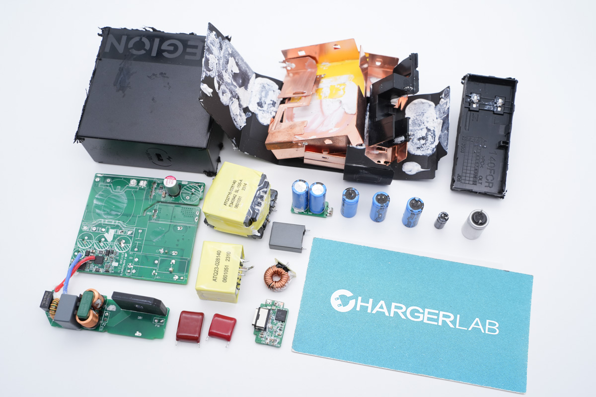
OK, that’s all for the Teardown of Apple 140W GaN USB-C charger. Let’s take a “family portrait.”
Summary of ChargerLAB
As the first charger that supports USB PD3.1. This 140W GaN charger still maintains Apple’s consistent high quality. Most of the controllers and MOSFETs are customized models and come from internationally renowned manufacturers such as ST, Infineon, ON Semiconductor, Toshiba, etc.
In addition, there are two GaNFETs, which is the first time Apple uses GaN chips in their chargers. And the electrolytic capacitor for filtering comes from Japanese Rubycon.
Until now, we can understand why it can be sold for $99.
As the industry leader, the first PD3.1 and GaN charger from Apple means more and more manufacturers will follow up very quickly. Hope more devices and chargers can support PD3.1 in the future.

