Introduction
As the PD3.1 protocol is equipped on more devices, more third-party chargers on the market can support 140W now. And today, we got a 140W multi-port charger from Baseus, equipped with two USB-C ports and a USB-A port. So let's go ahead and take it apart to see how it works.
Product Appearance
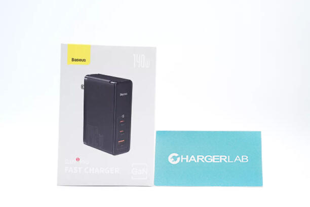
The front of the box is printed with Baseus logo and the product itself. It is called the "GaN 5 Pro Fast Charger".
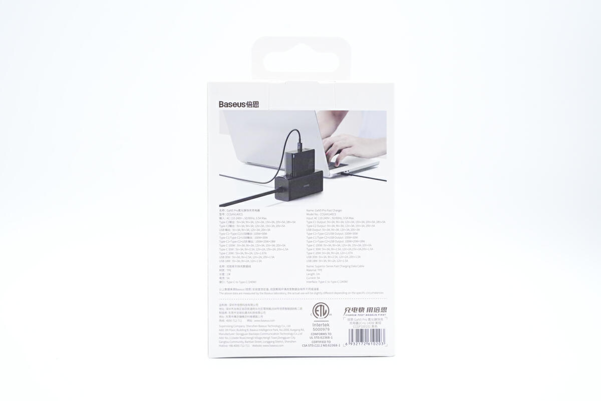
The specs info in different languages are printed on the back.
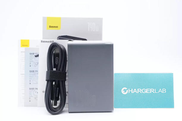
The box includes the charger, cable, user manual, warranty card and cartoon stickers. The charger is wrapped with an anti-scratch film for protection.
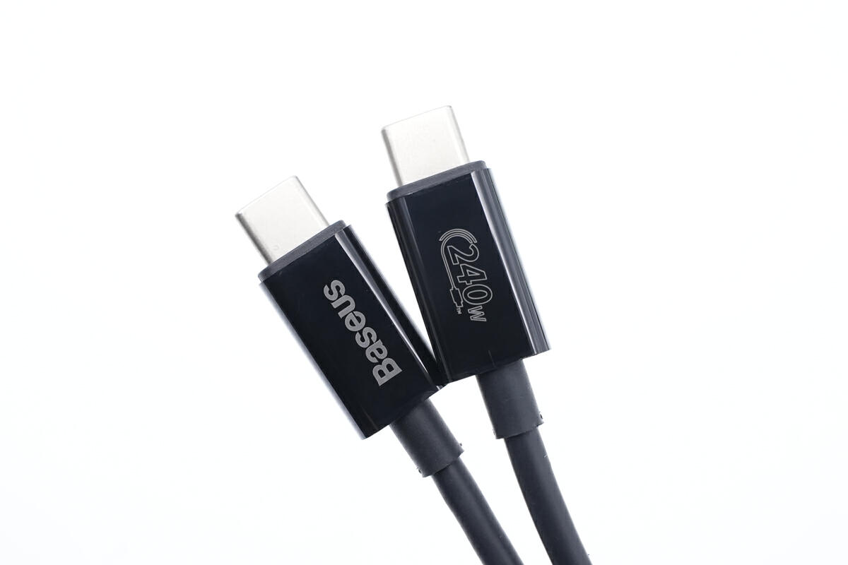
This is a 240W dual USB-C cable, which can fully support 240W and PD3.1 protocol.
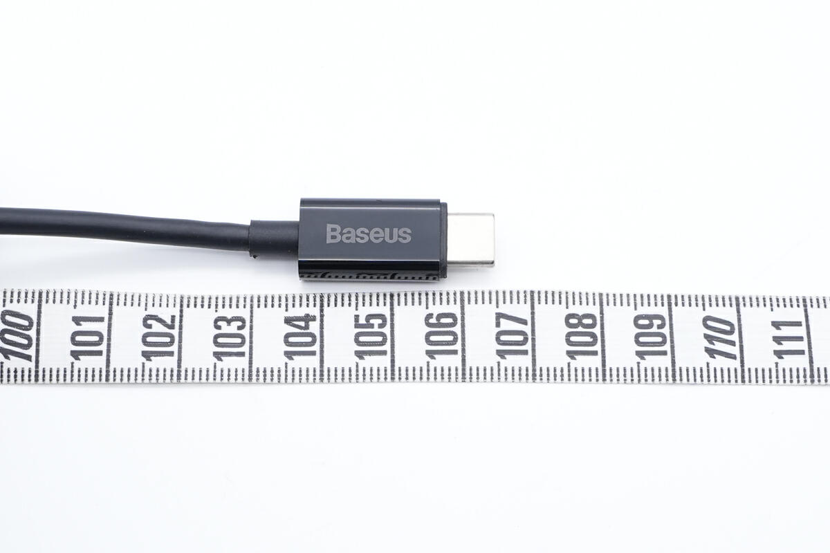
The length is about 1.06m (3' 5.73'').
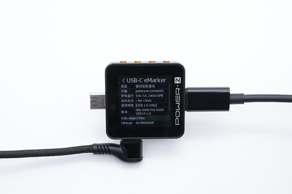
The ChargerLAB POWER-Z KM002C shows that this is a USB 2.0 cable and supports 240W super fast charging.
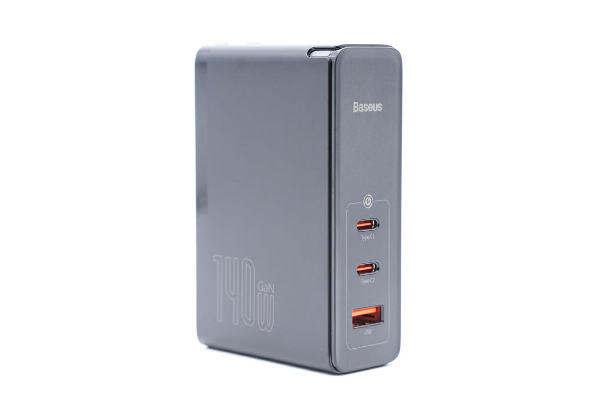
The charger is pretty like the Apple 140W charger with a rectangular shape, but with two more USB ports.
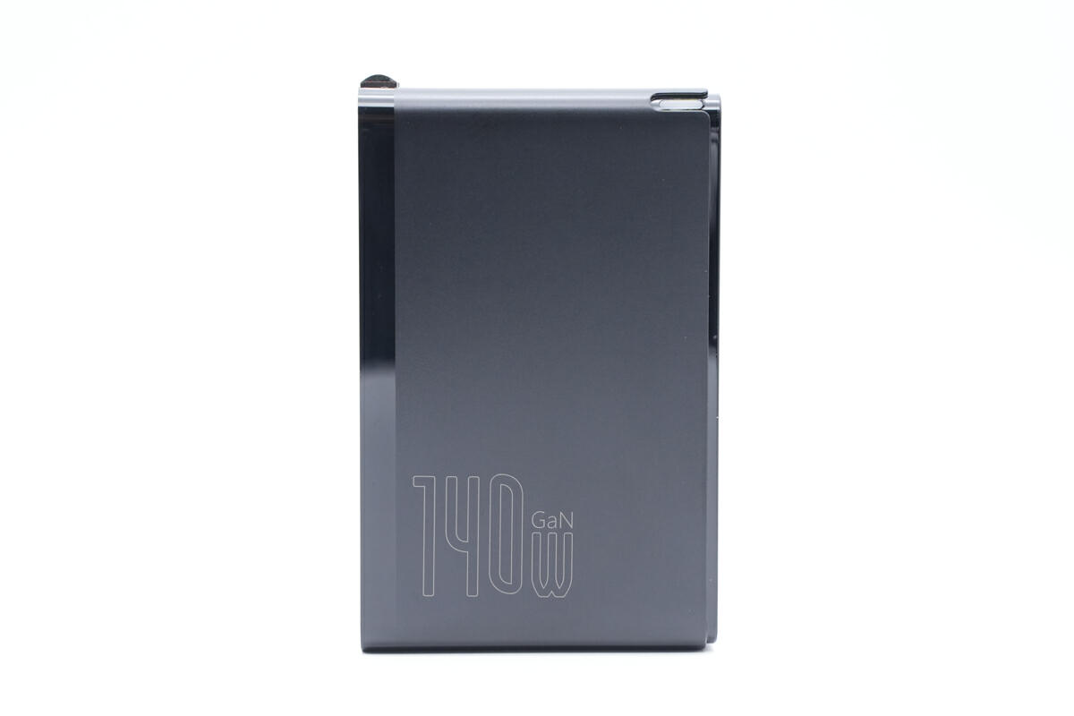
It adopts a black matte design with the 140W GaN printed on the side.
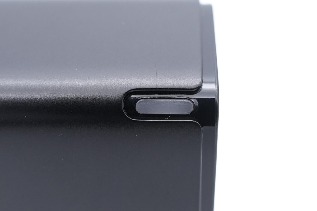
A small indicator light is at the corner.
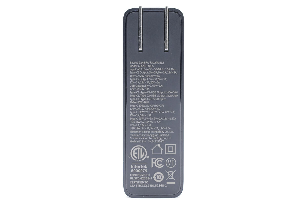
This charger has passed ETL, FCC certification.
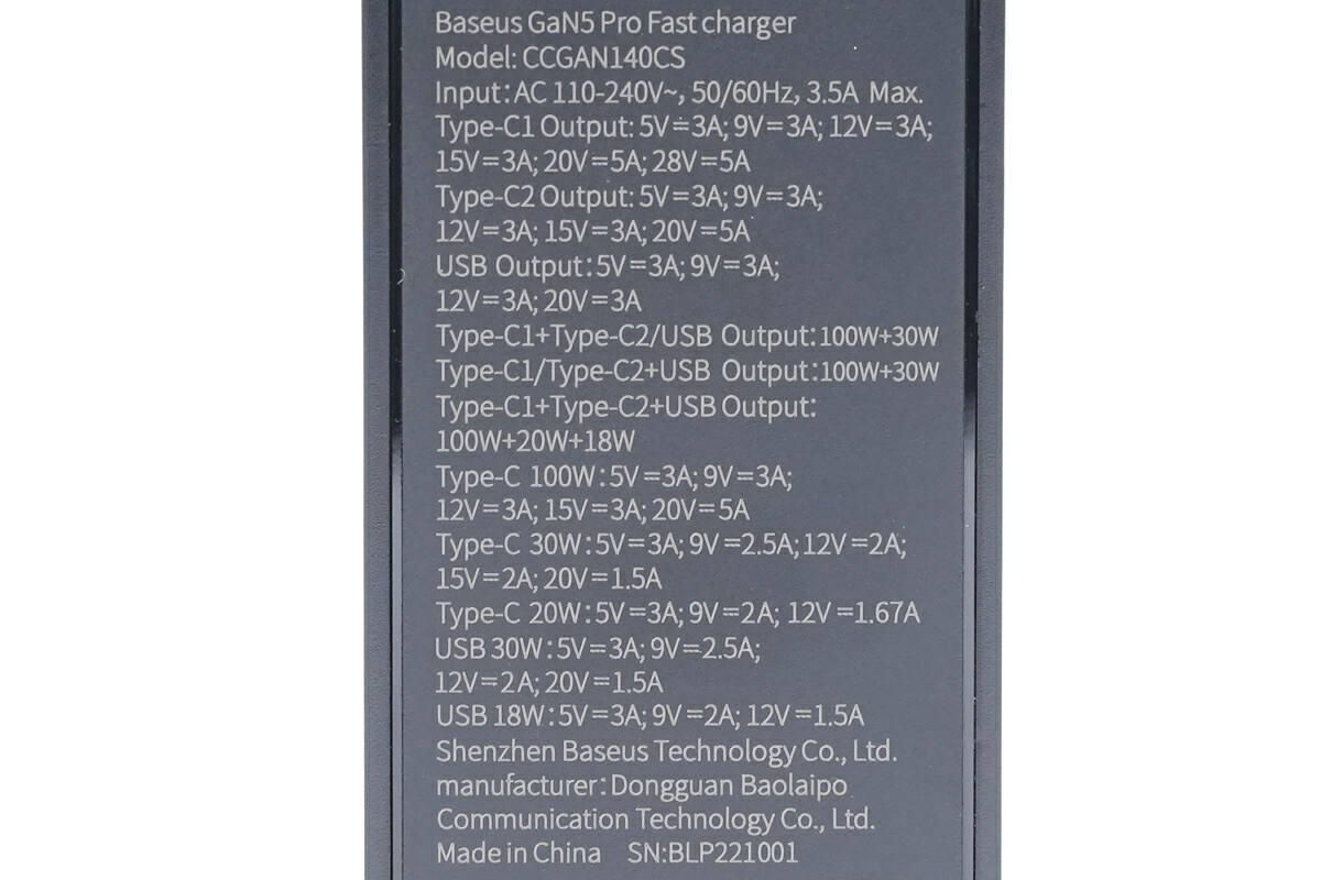
The specs info is very complicated. The model is CCGAN140CS. It can support input of 110-240V 50/60Hz 3.5A. Only the USB-C1 can support 140W, and the other USB-C port can only support up to 100W. And when charging multiple devices, the 140W output will be distributed automatically. The manufacturer is Baolaipo Communication.
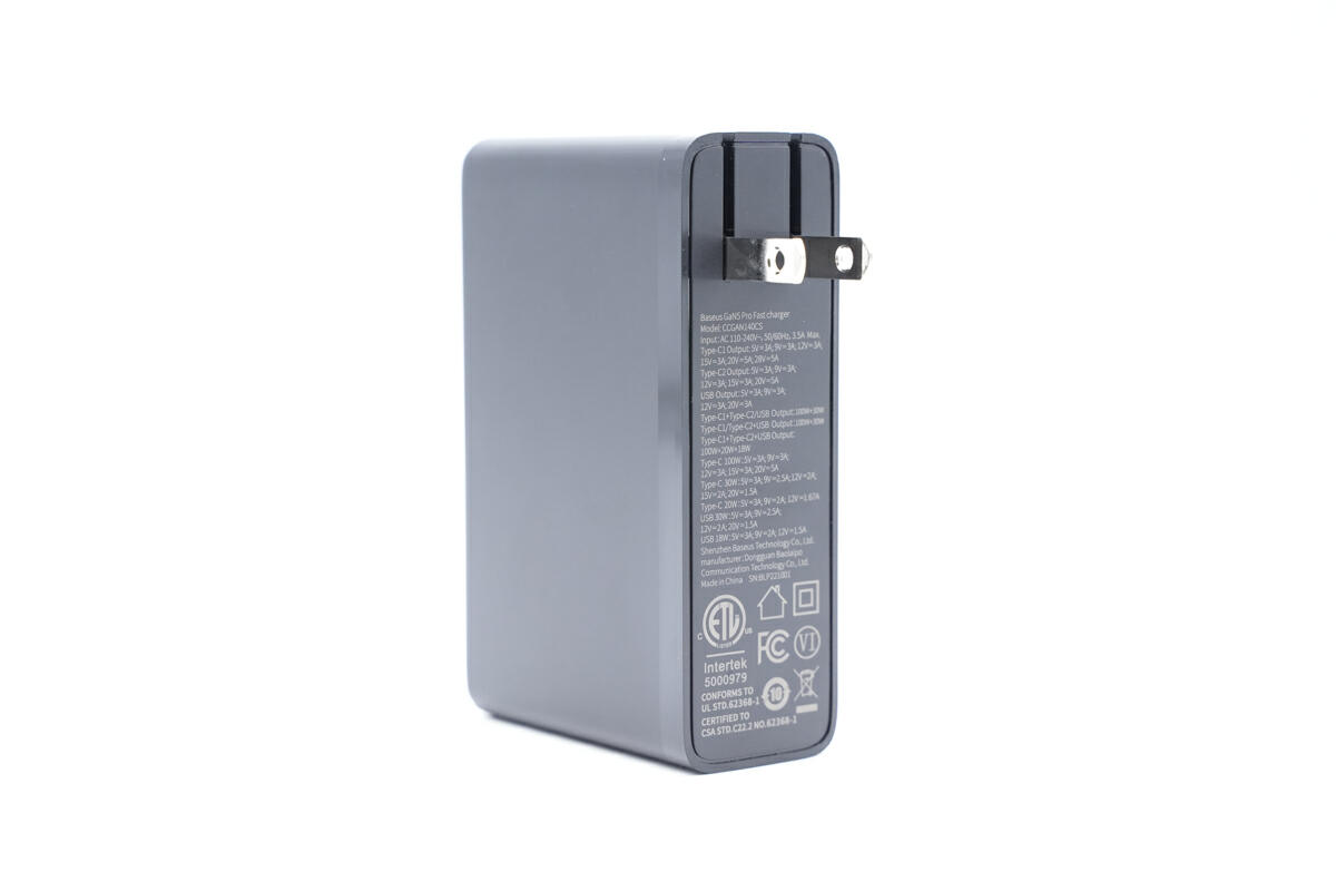
The input prongs can be folded, which is easy to carry around.
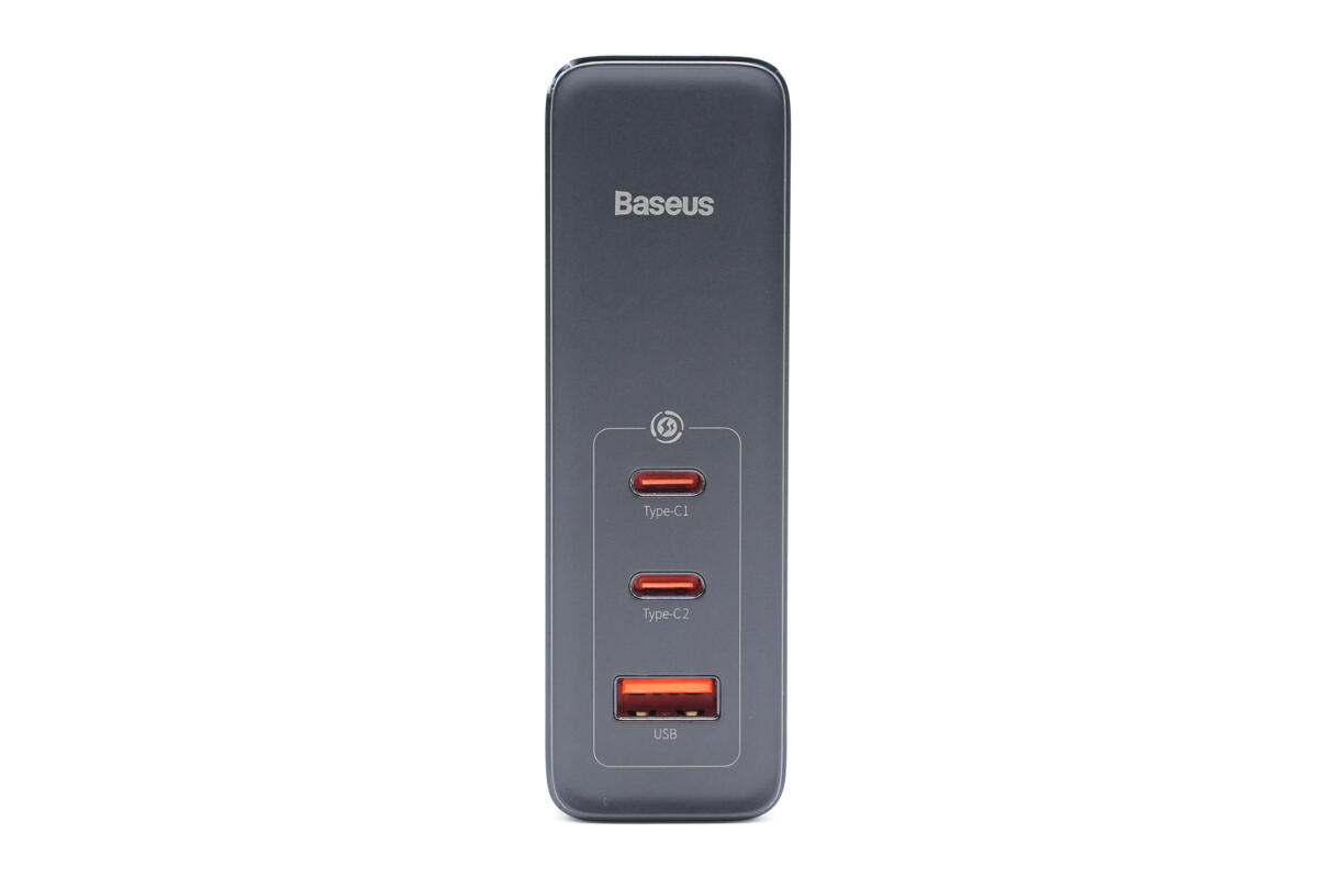
All the USB ports at the output panel are orange. And the C1 and C2 are printed below the USB ports.
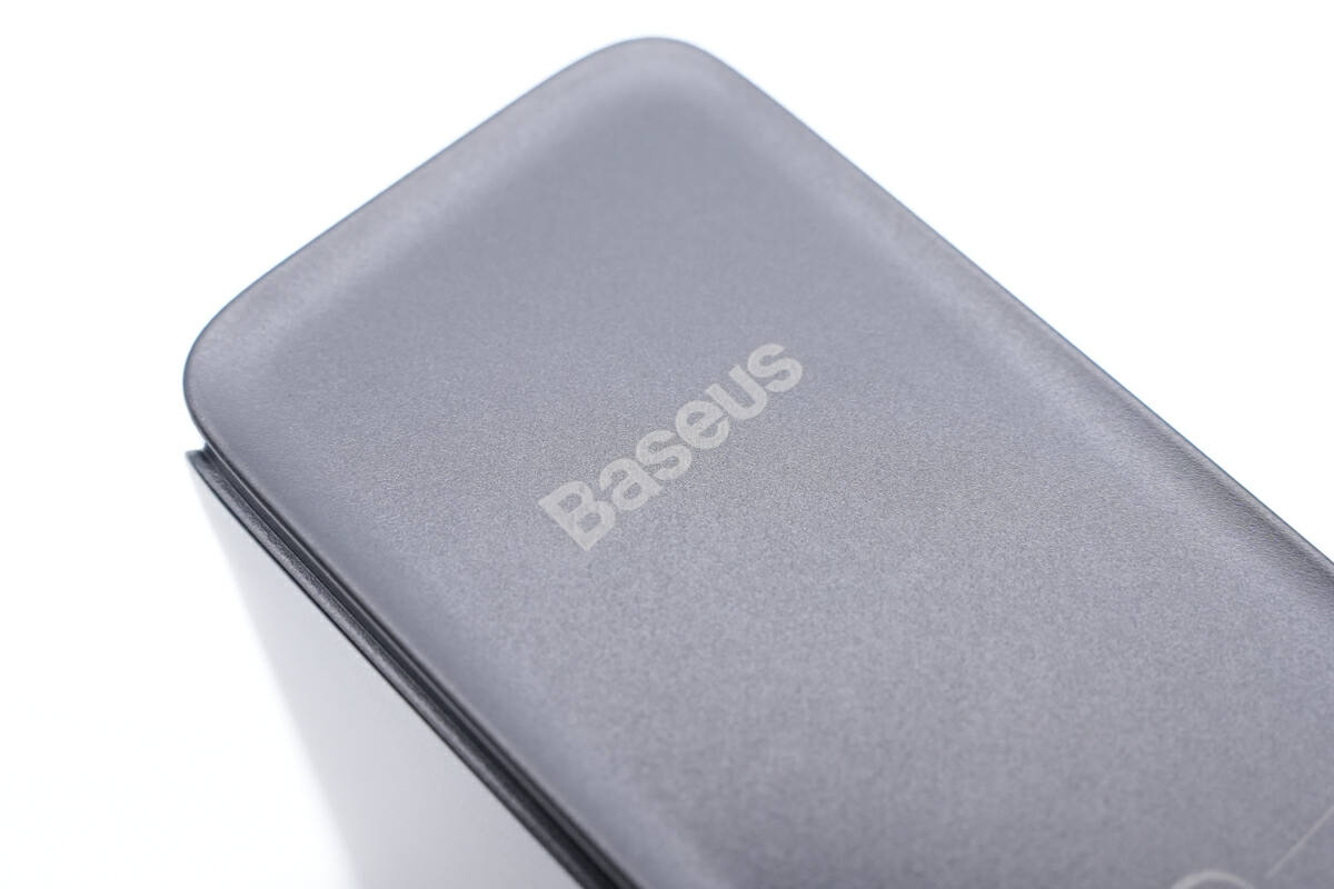
The baseus logo is above them.
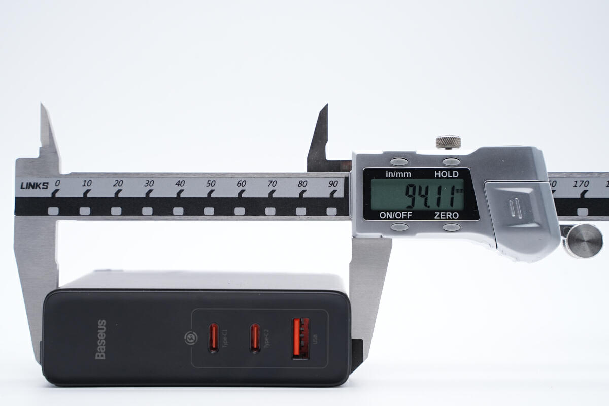
The length of the charger is about 94mm (3.7 inches).
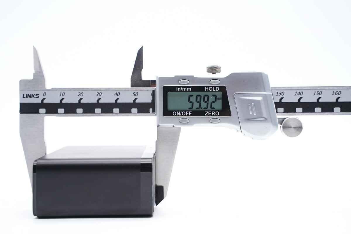
The width is about 60mm (2.36 inches).
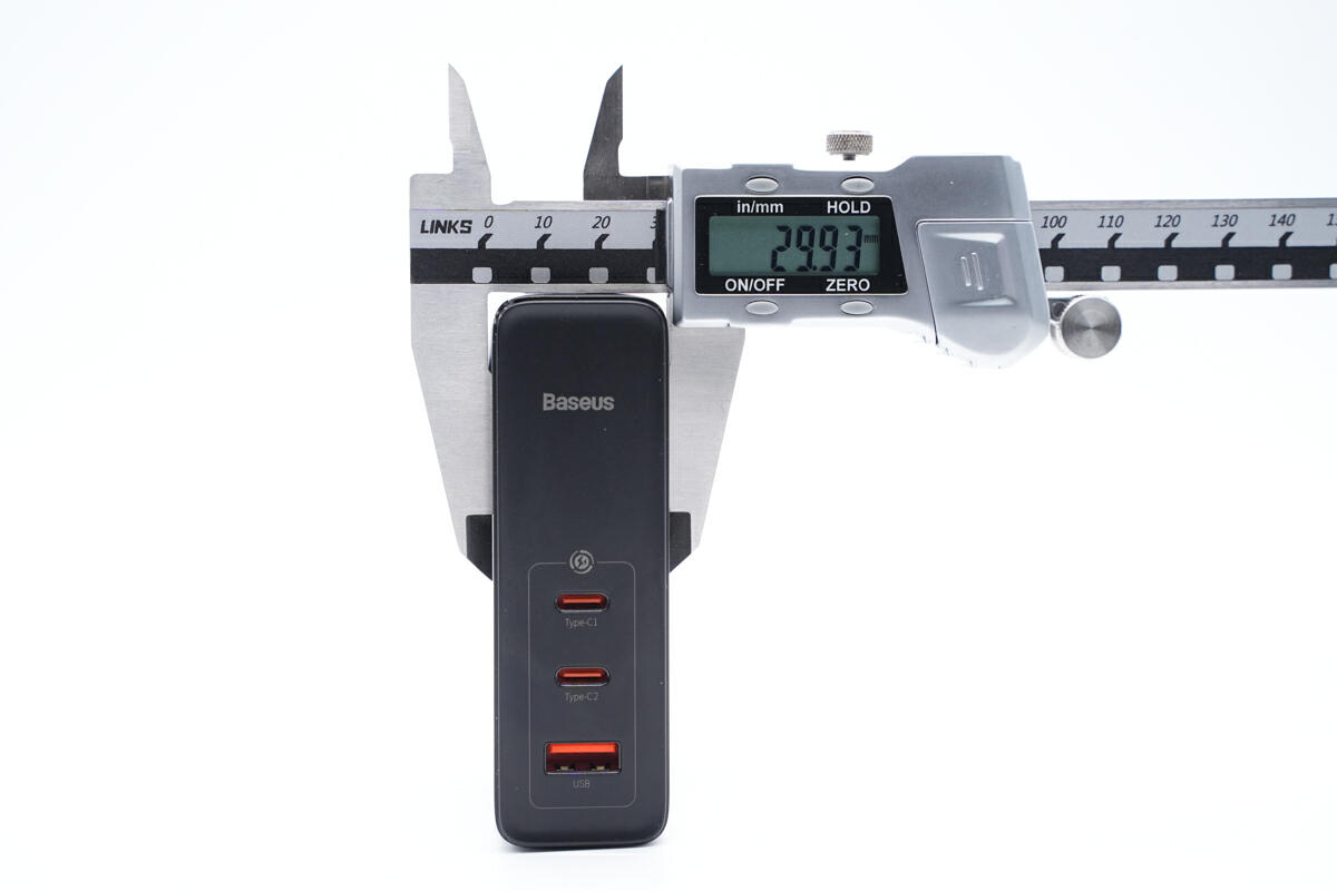
And the height is about 30mm (1.18 inches).
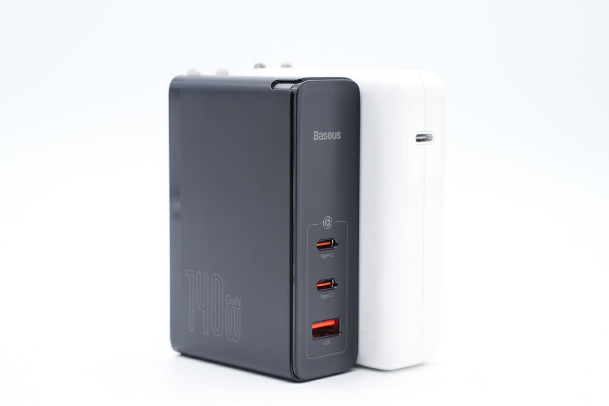
Compared with Apple 140W charger, the size is almost the same.
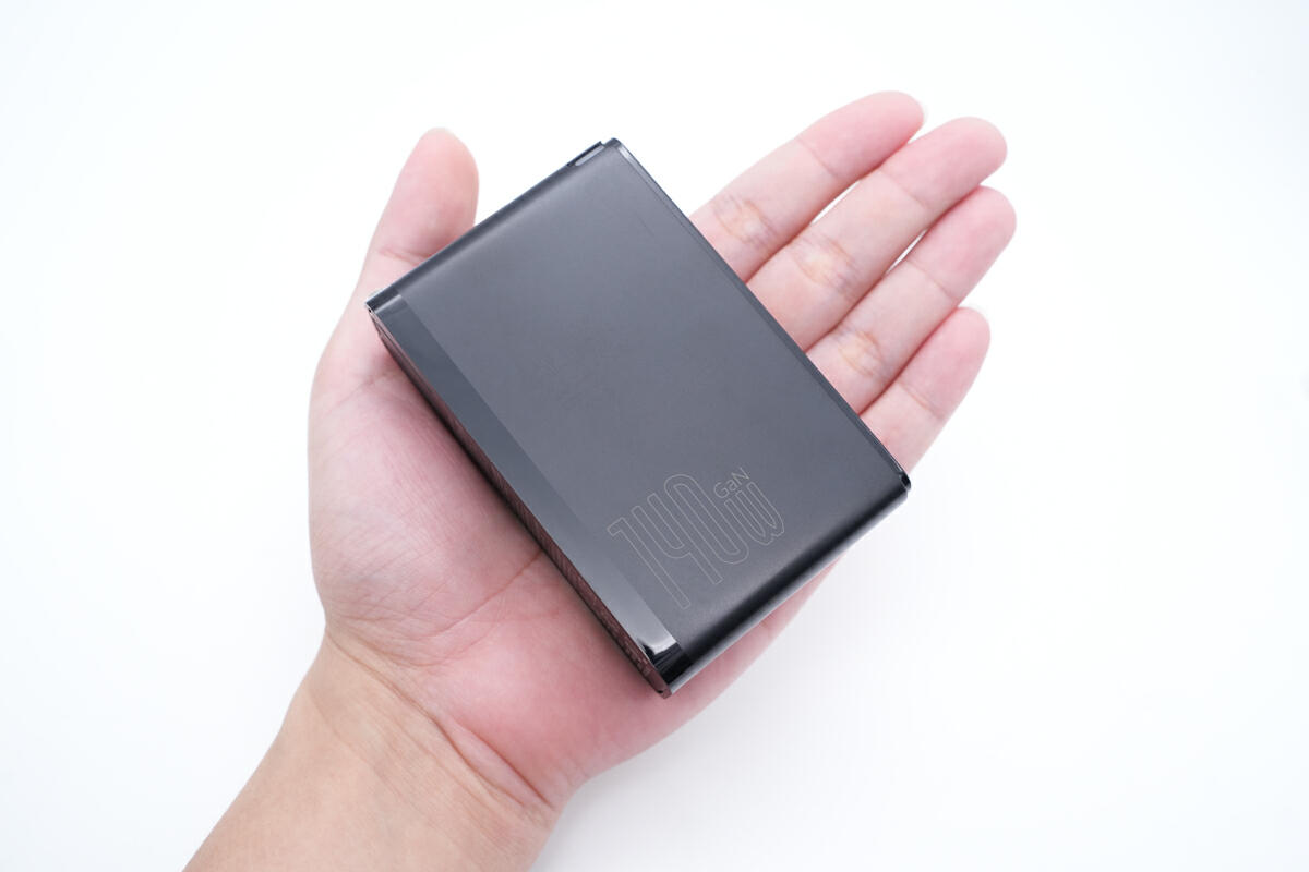
This is how it looks like on my hand.
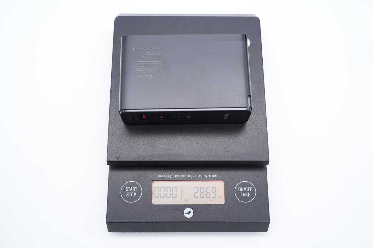
And the weight is about 287g (10.12 oz).
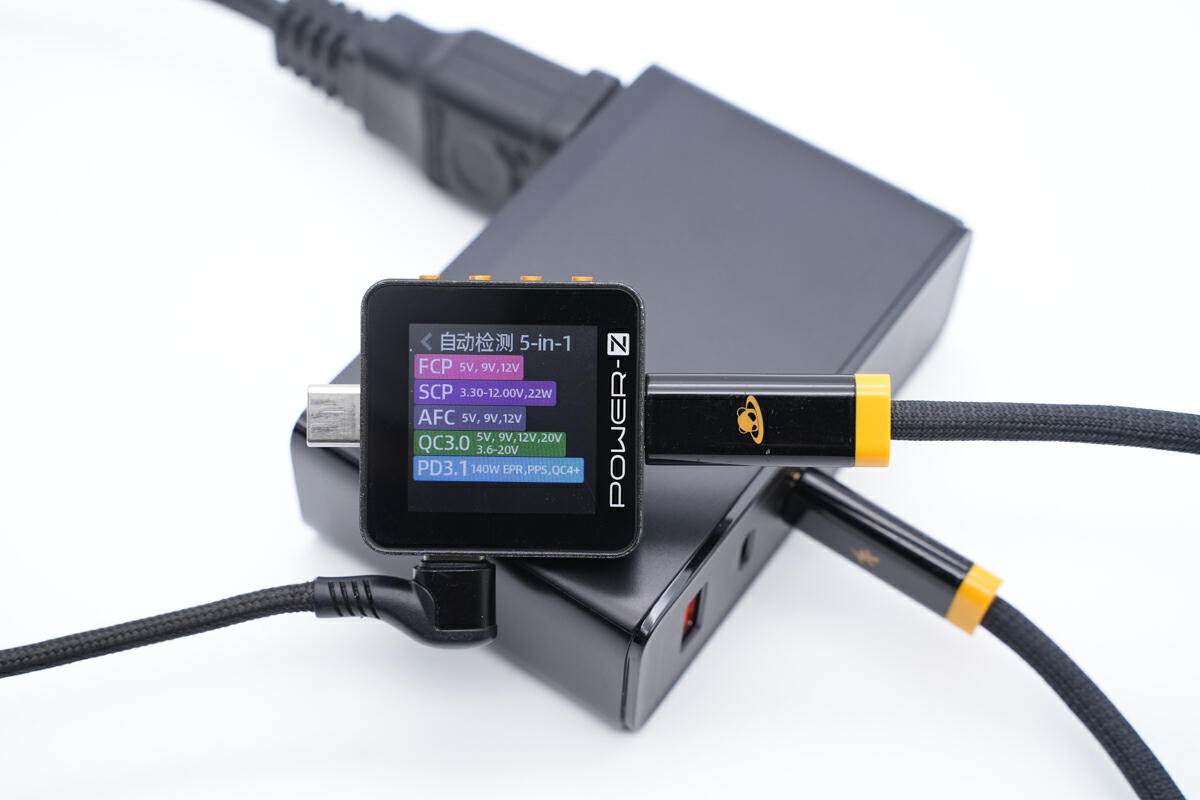
The ChargerLAB POWER-Z KM002C shows USB-C1 supports FCP, SCP, AFC, QC3.0/4+, PD3.1, and PPS protocols.
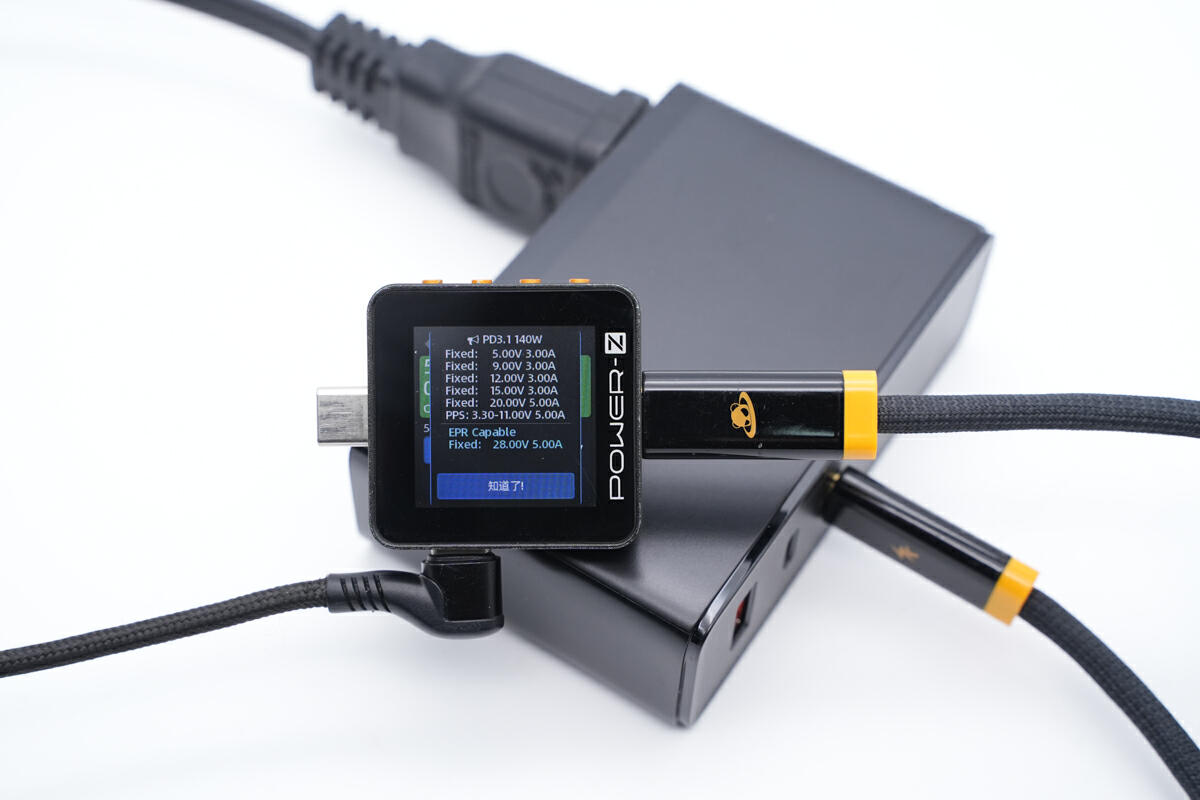
It also supports six fixed PDOs of 5V3A, 9V3A, 12V3A, 15V3A, 20V5A, 28V5A, and a set of PPS.
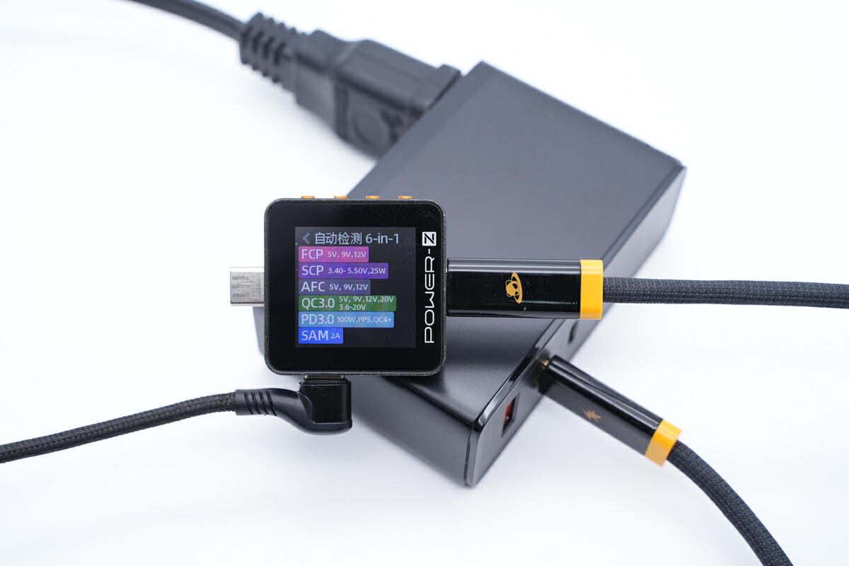
And the USB-C2 supports FCP, SCP, AFC, QC3.0/4+, PD3.0, and PPS protocols.
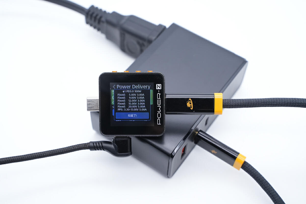
It can support five fixed PDOs of 5V3A, 9V3A, 12V3A, 15V3A, 20V5A, and a set of PPS.
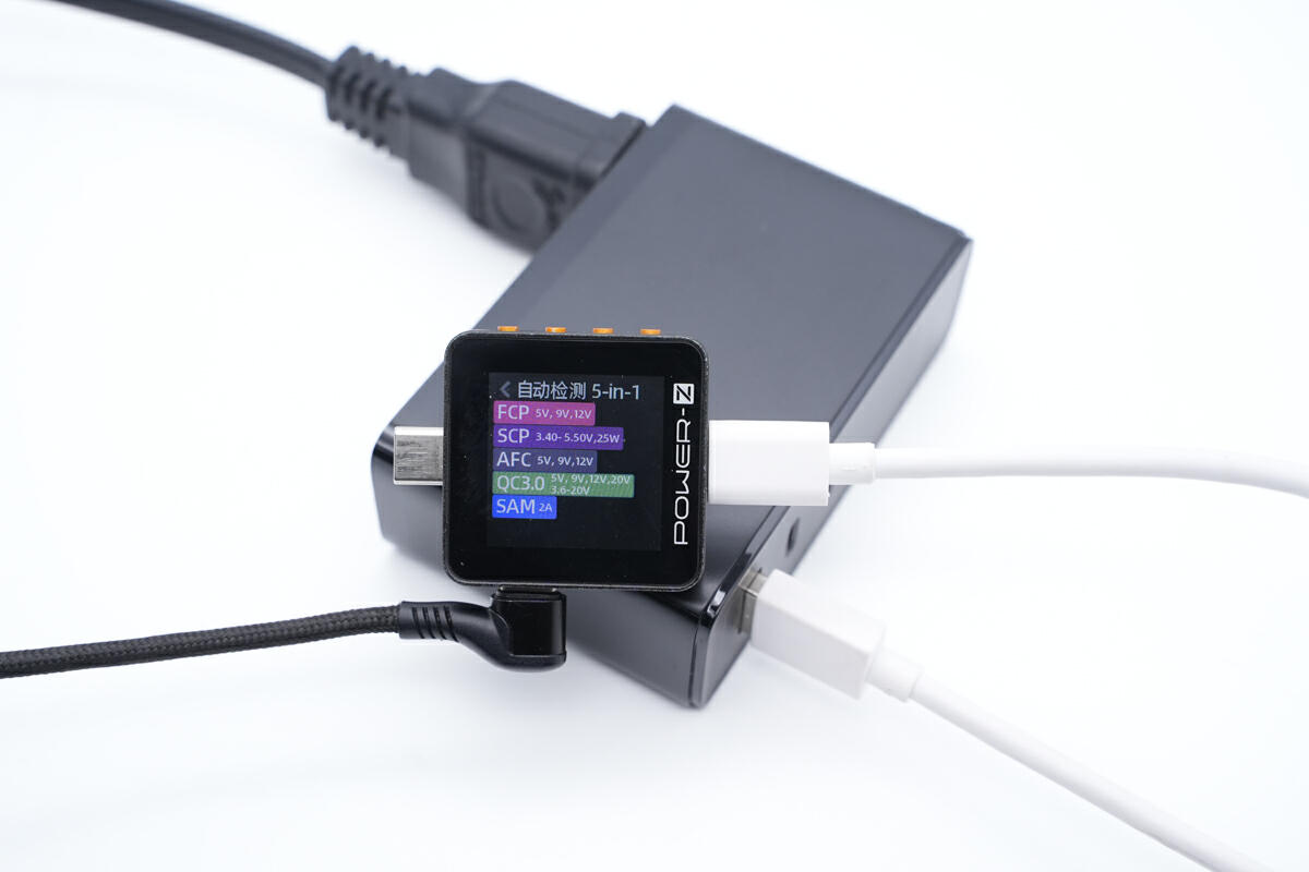
Finally, the USB-A supports FCP, SCP, AFC, and QC3.0 protocols.
Teardown
Next, we gonna take it apart to check out the internal components and structure.
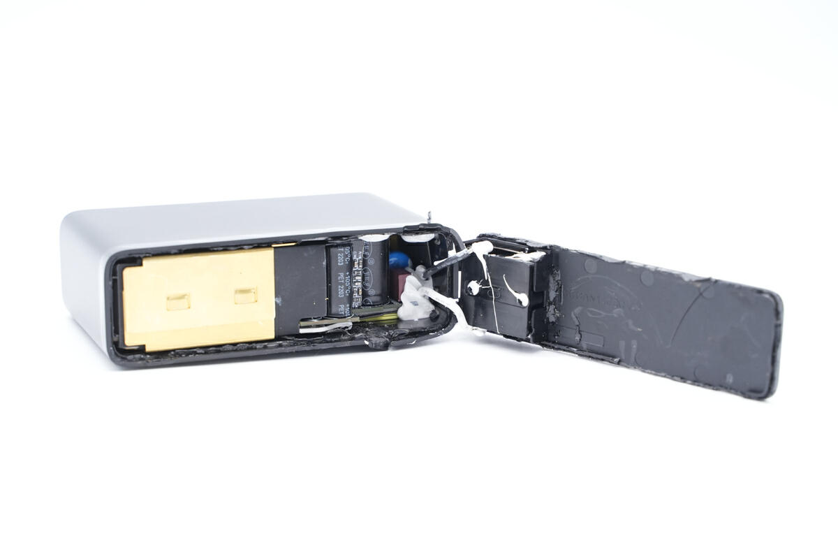
Firstly, remove the bottom cover, we can see a large area of pure copper heat sinks.
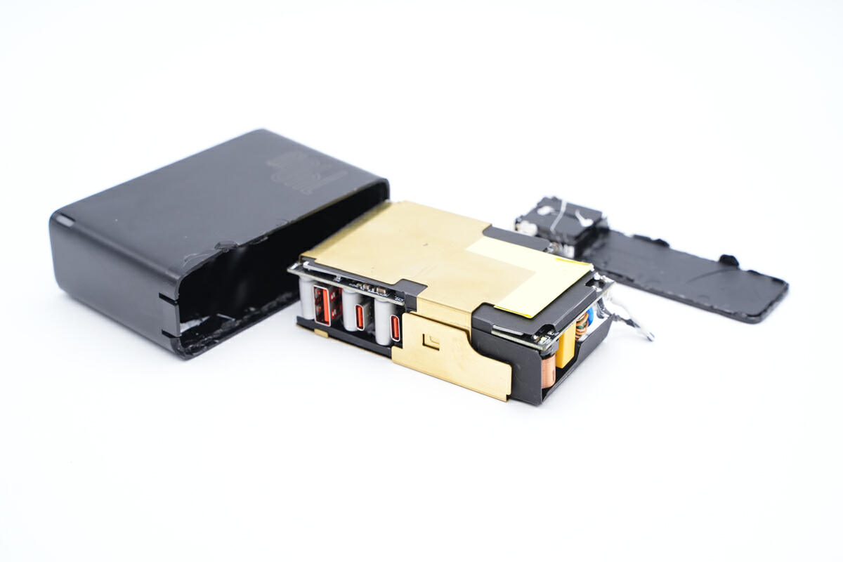
The entire module is covered by the heat sinks, and a layer of black Mylar sheet for insulation is under it.
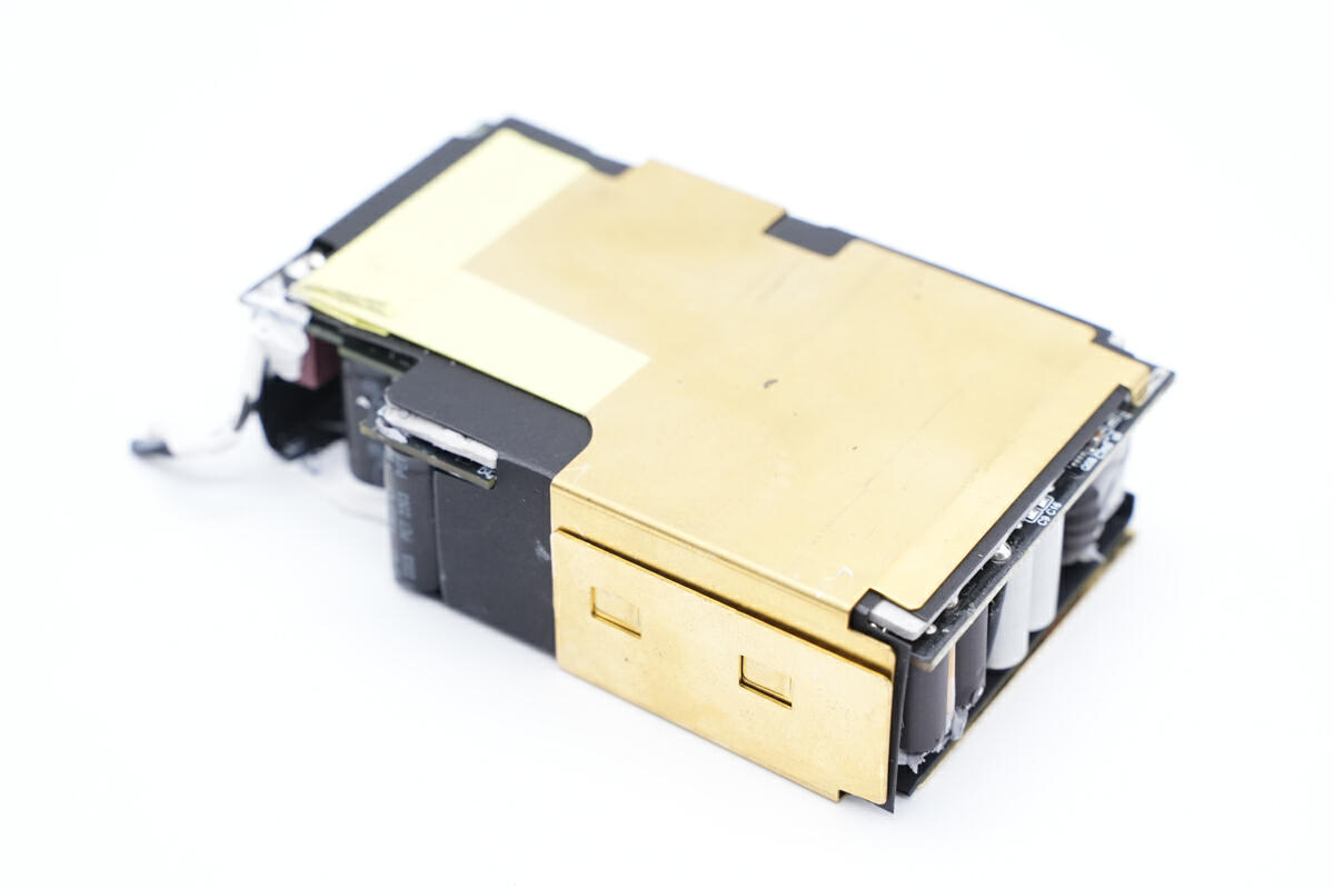
These two heat sinks are connected together on this side.
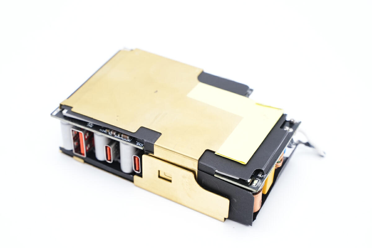
And also on the other side.
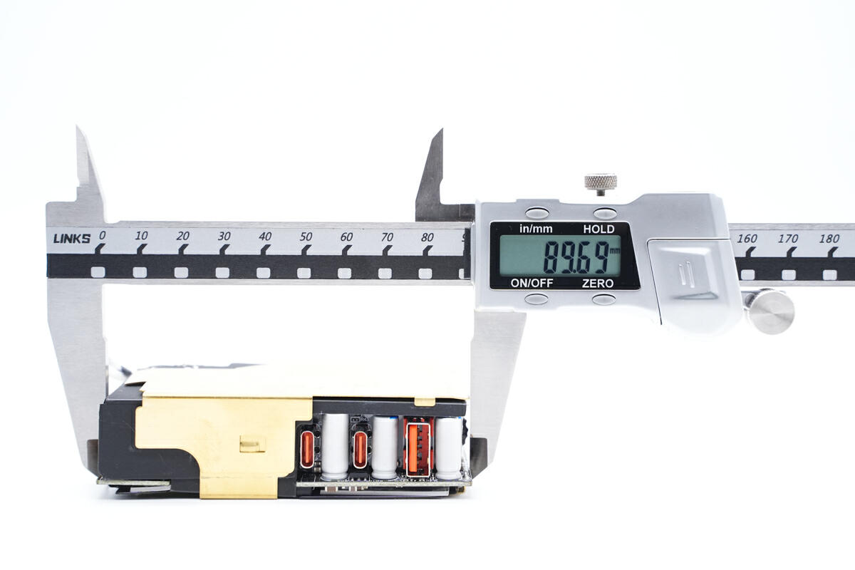
The length of the PCBA is about 90mm (3.54 inches).
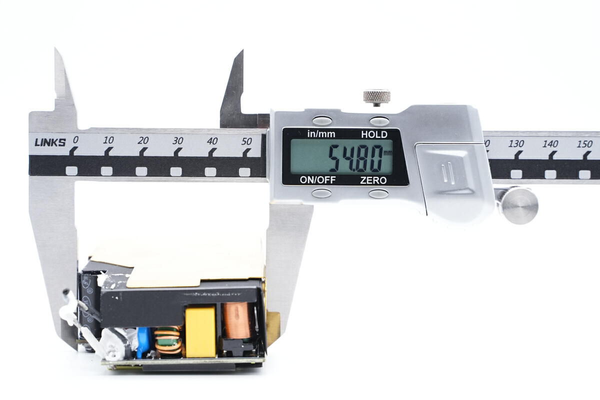
The width is about 55mm (2.17 inches).
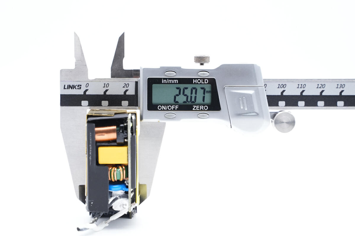
And the height is about 25mm (0.98 inches).
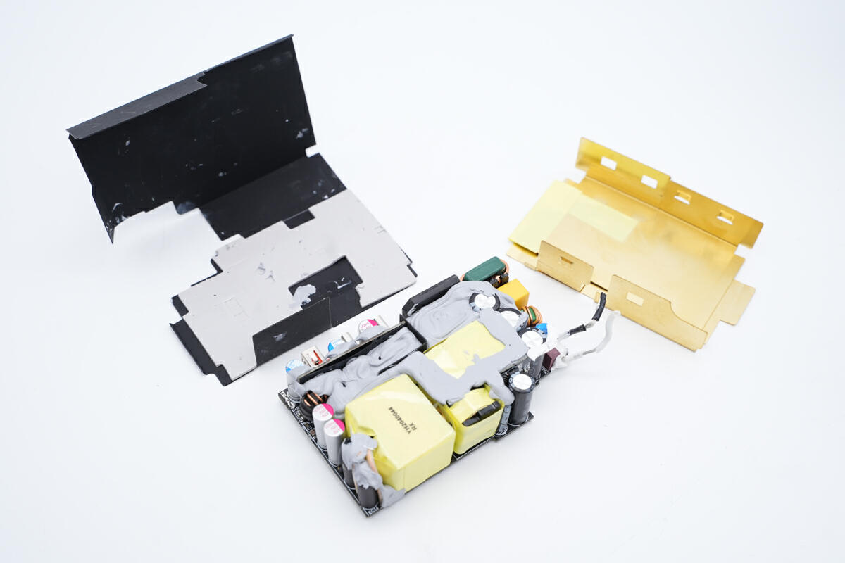
Remove the heat sinks outside the PCBA module, the Mylar sheet has a thermal pad to dissipate heat.
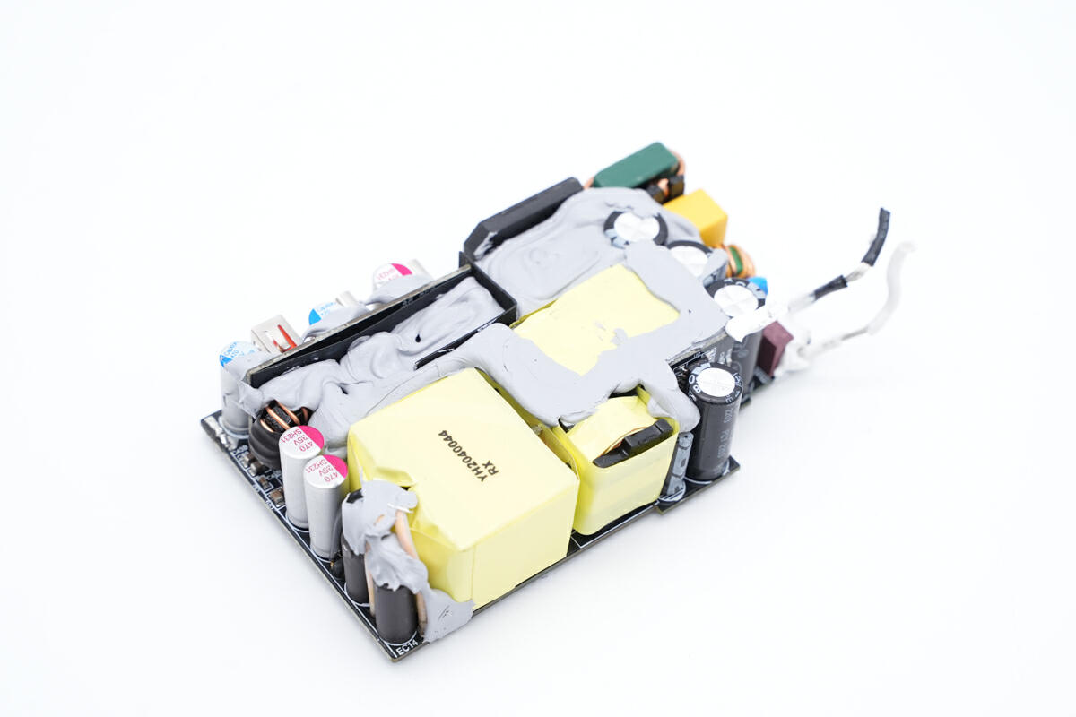
The gaps between different components are filled with gray silicone adhesives. It can fix the components and dissipate heat.
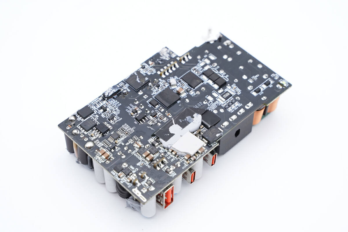
A Mylar sheet is inserted into the PCBA module and fixed with adhesives for insulation between primary and secondary side.
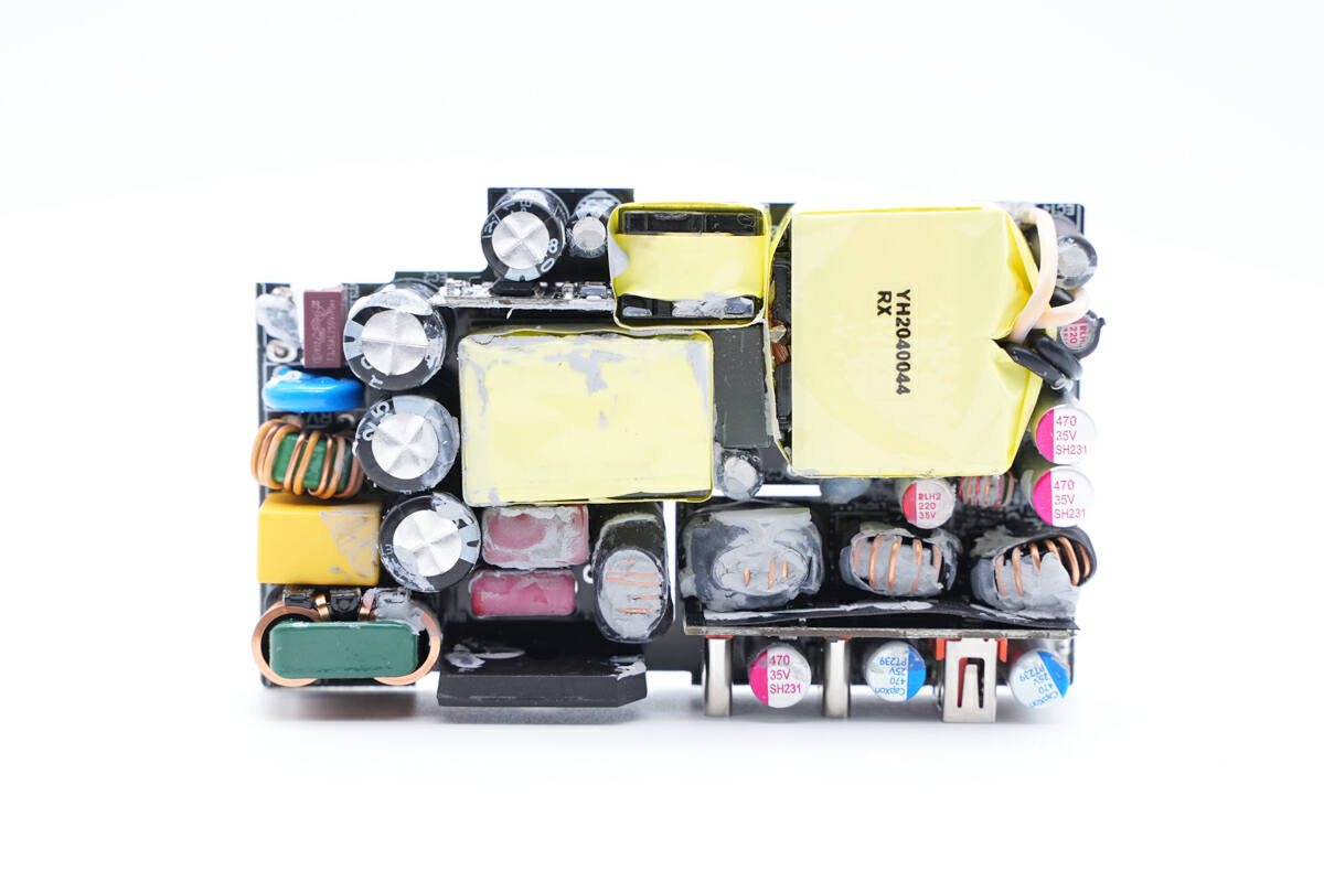
Clean up the PCBA module. The AC input, fuse, varistor, common mode choke, safety X2 capacitor and the secondary common mode choke are on the left. The rectifier bridge, filter inductor and filter capacitor are on the right side of the common mode choke. Above is the PFC boost inductor. A high voltage filter capacitor is on the left of the PFC boost inductor.
There is a small PCB above the PFC boost inductor, and there is a primary master control chip on it. On the right side of the PFC boost inductor are the resonant capacitor and inductor. The inductor and small PCB are below the transformer, and the layout is very compact.
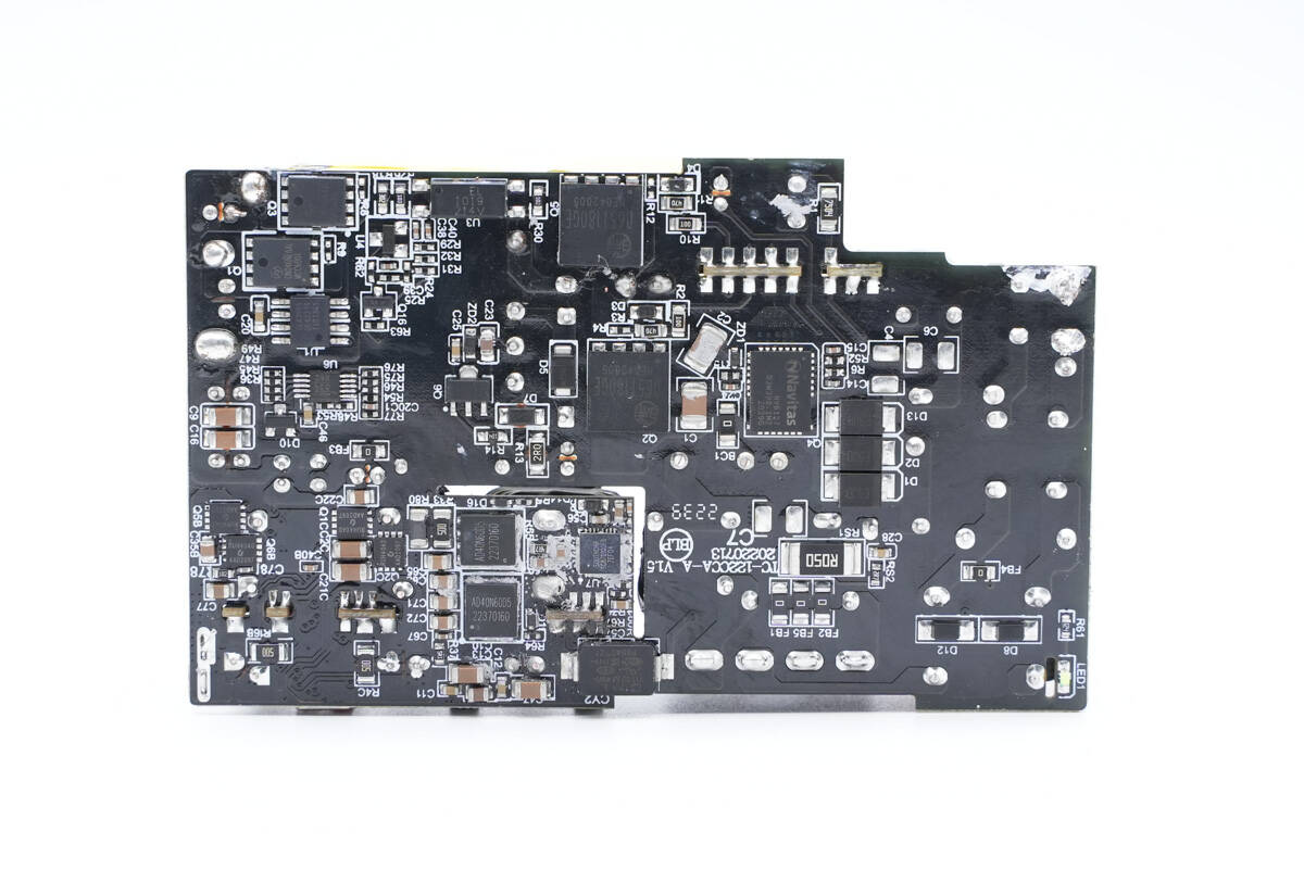
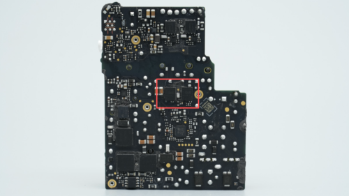
Flip to the back, the synchronous rectifier MOSFET and the controller are in the upper left corner, the LLC half-bridge MOSFET and the PFC boost MOSFET are on the right. The buck MOSFET and buck-boost controller are on the low-voltage side, and there is an MCU for secondary control.
ChargerLAB found it adopts LLC topology and has a PFC circuit. The 140W USB-C port adjusts the output voltage through a buck-boost circuit, and the 100W USB-C and USB-A port output through a buck circuit to achieve independent fast charging of the three ports.

The AC input is connected to the PCBA through two wires, and the solder joint is reinforced with adhesives.
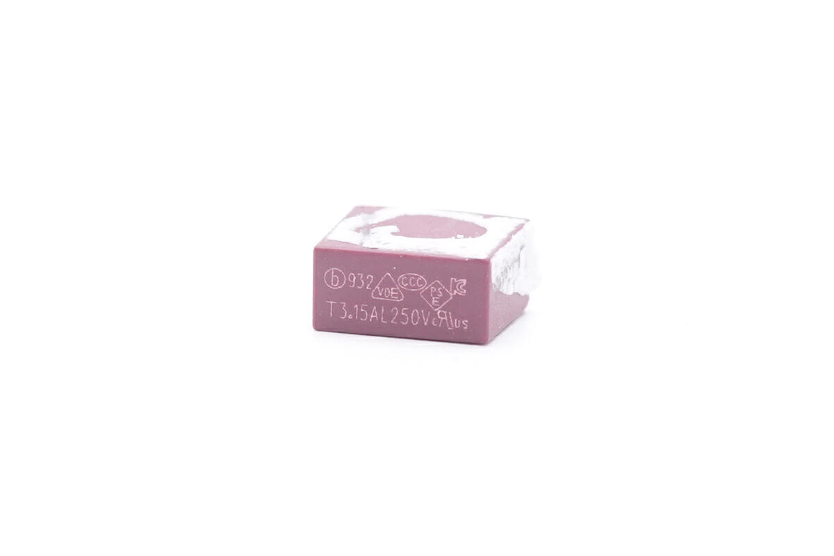
The time-delay fuse is from Better Electronics. 3.15A 250V.
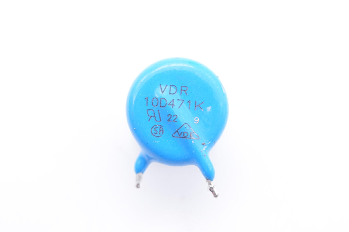
This blue varistor marked with 10D471K is used for overvoltage protection.
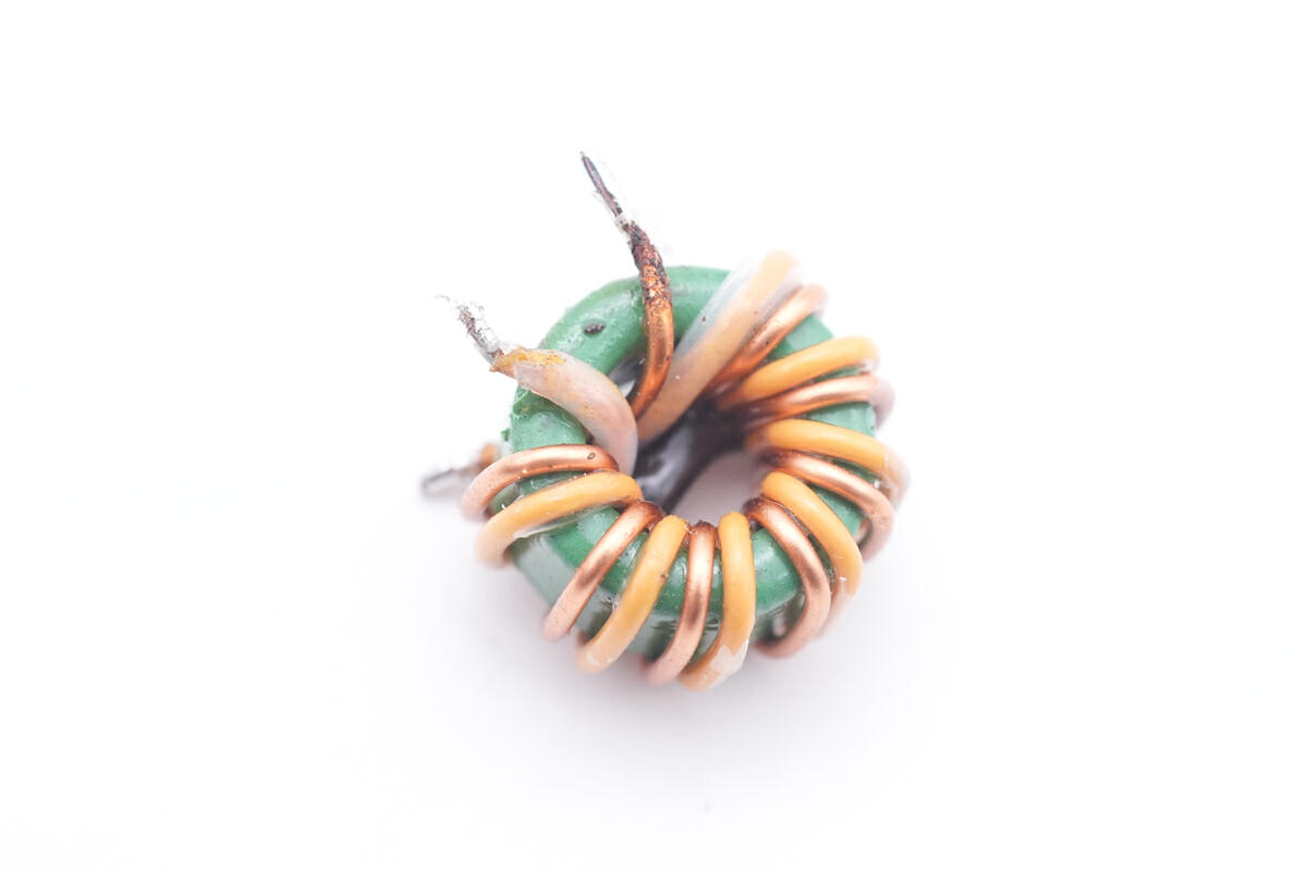
The first common mode choke is wound with magnet wires and insulated wires.
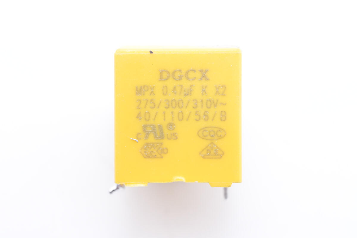
The safety X2 capacitor is from DGCX. 0.47μF.
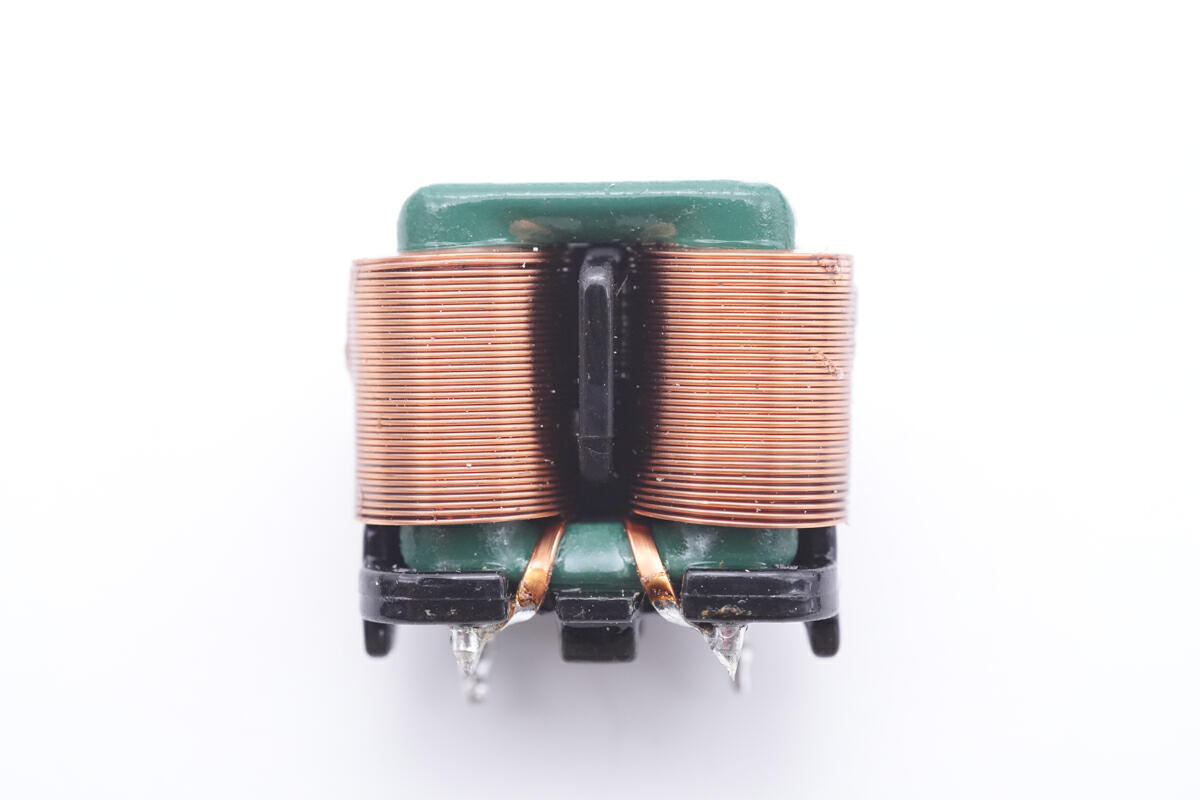
The second common mode choke is wound with flat copper wires.
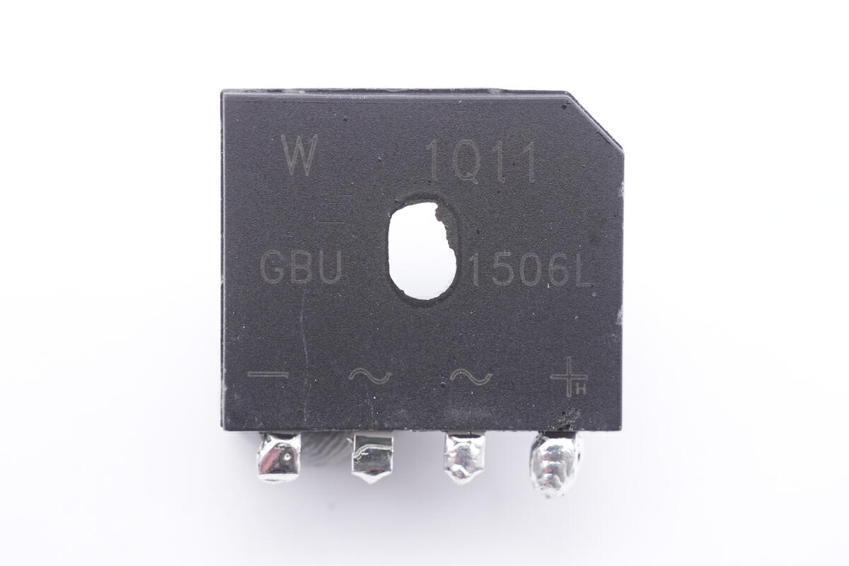
The model of the bridge rectifier is GBU1506. 15A 600V.
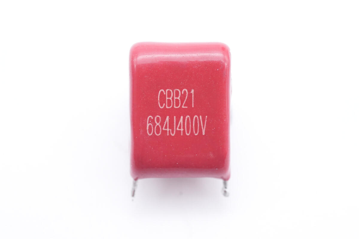
This film filter capacitor is 0.68μF 400V.
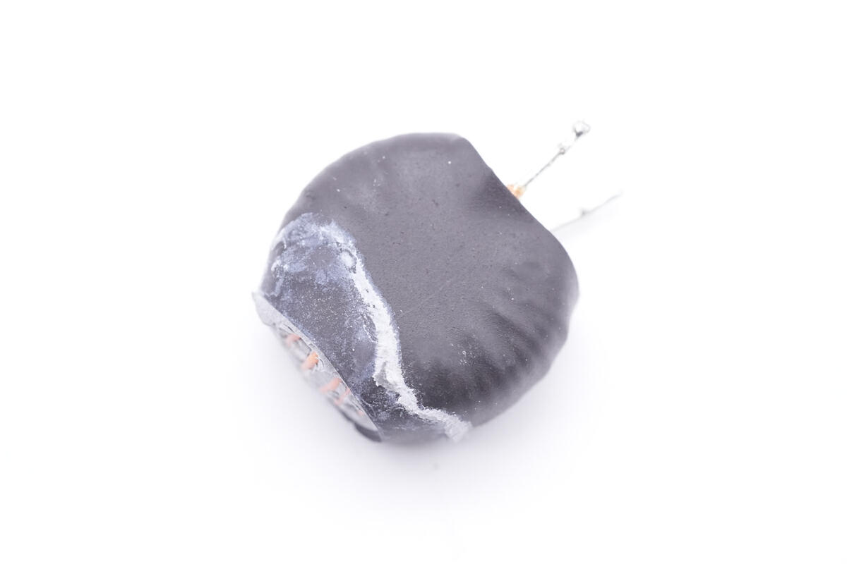
The filter inductor is insulated by heat shrinkable tubing.
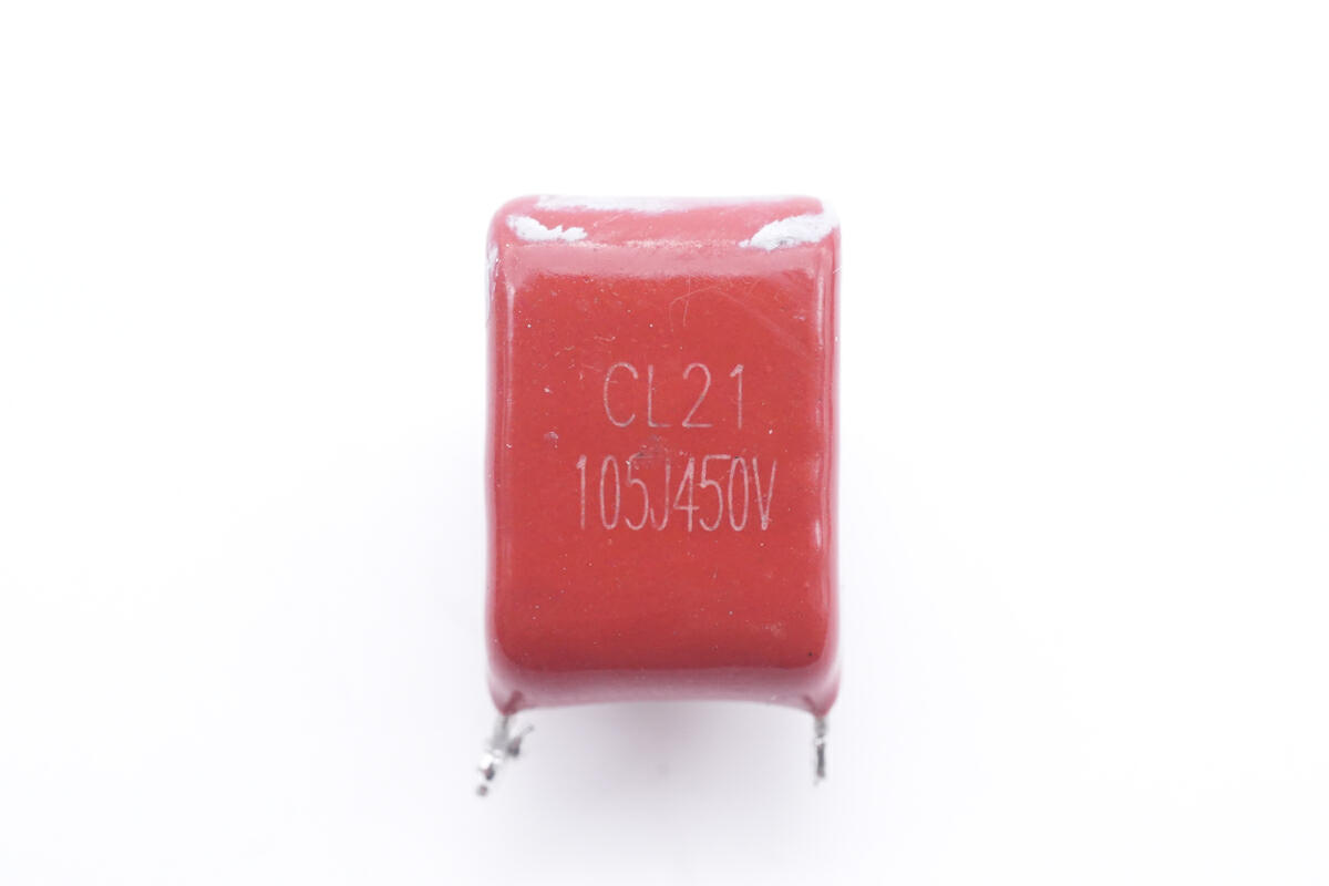
And this film filter capacitor is 1μF 450V.
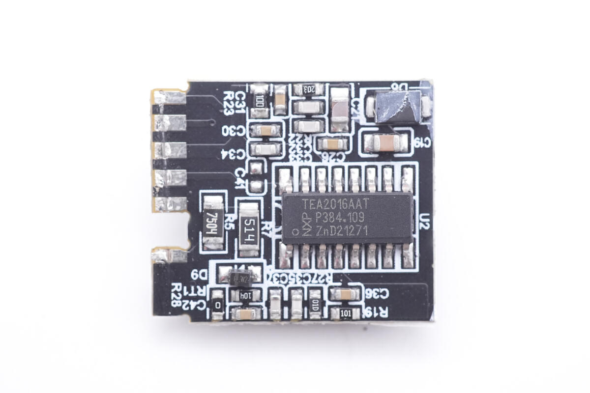
The primary controller of the charger is soldered on the front of the vertical PCB.
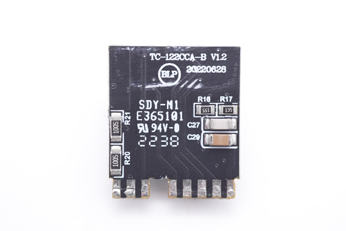
And the resistor capacitor is on the back.
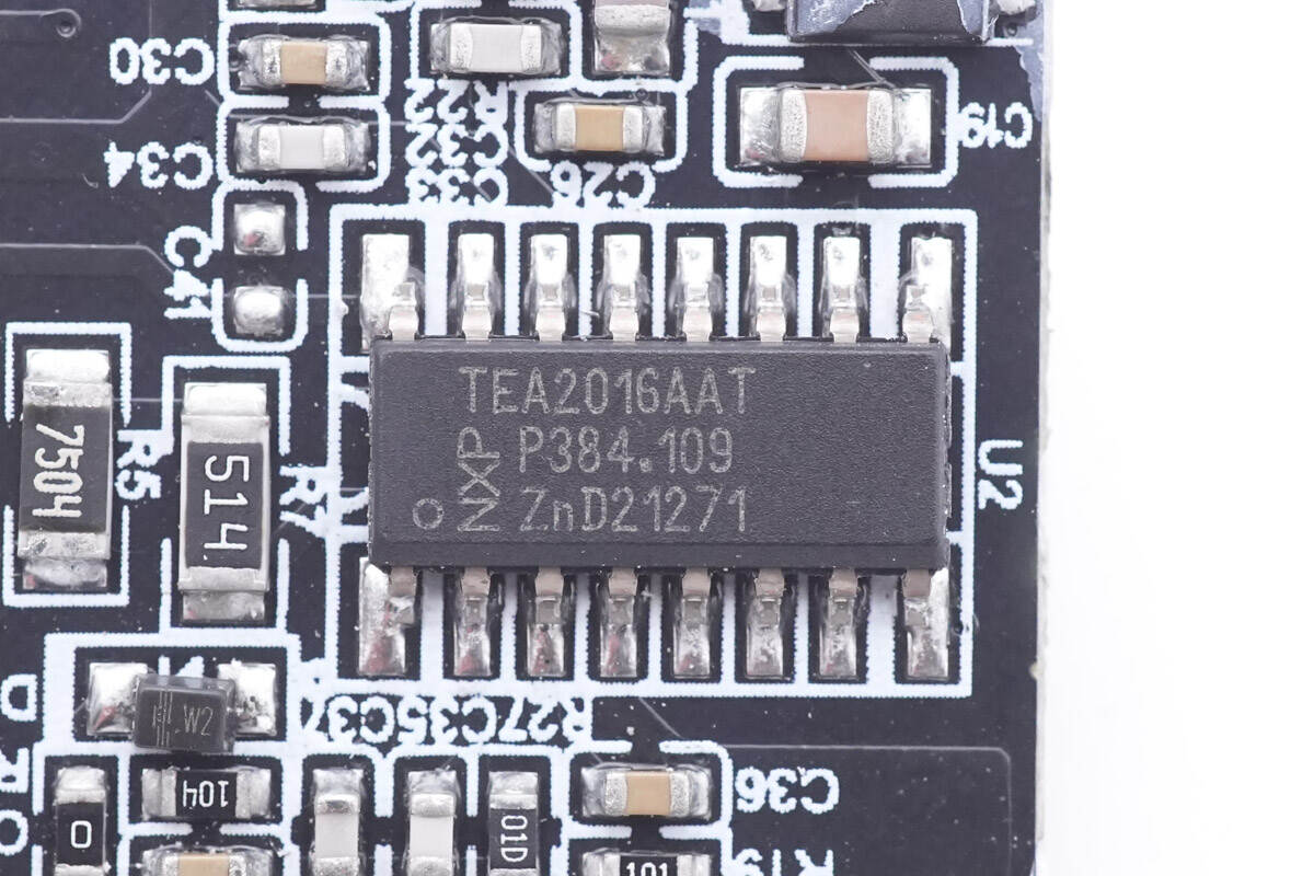
The primary PWM master control chip adopts NXP TEA2016AAT, which is a chip with built-in LLC controller and PFC controller. It integrates a digital architecture control, which simplifies the design and reduces the number of peripheral components. The chip has multiple protection features, and the integration level is very high.
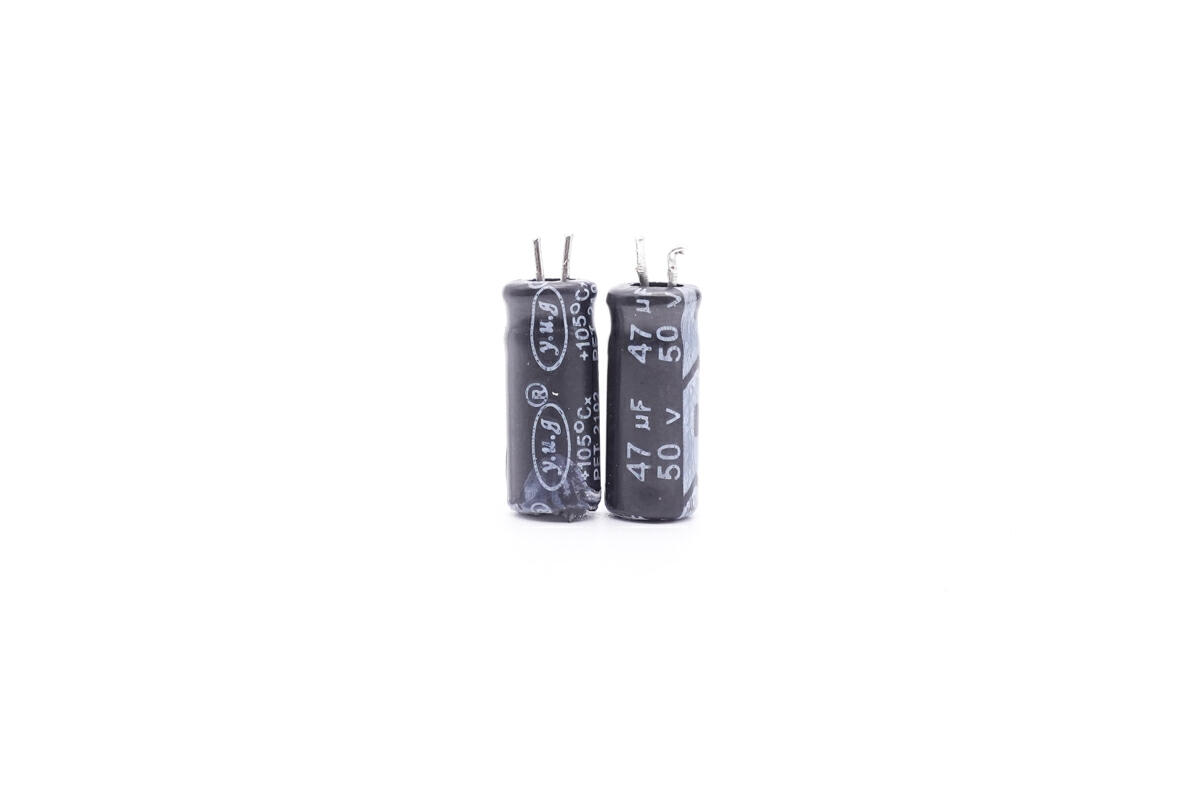
Those two tiny electrolytic capacitors from Yuguang Electronics can power the primary controller. 47μF 50V.
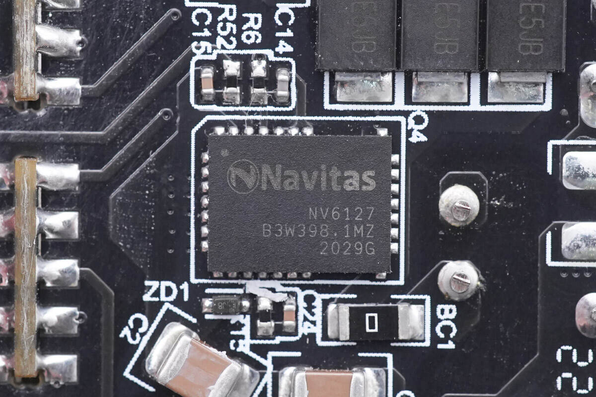
The NV6127 GaN IC for PFC circuit is from Navitas, which integrates GaN FET, GaN driver and logic circuit. It adopts QFN 6 x 8 package, with upgraded heat dissipation performance, 125mΩ resistance, and built-in driver to support 10-30V power supply. It also supports up to 2MHz switching frequency.
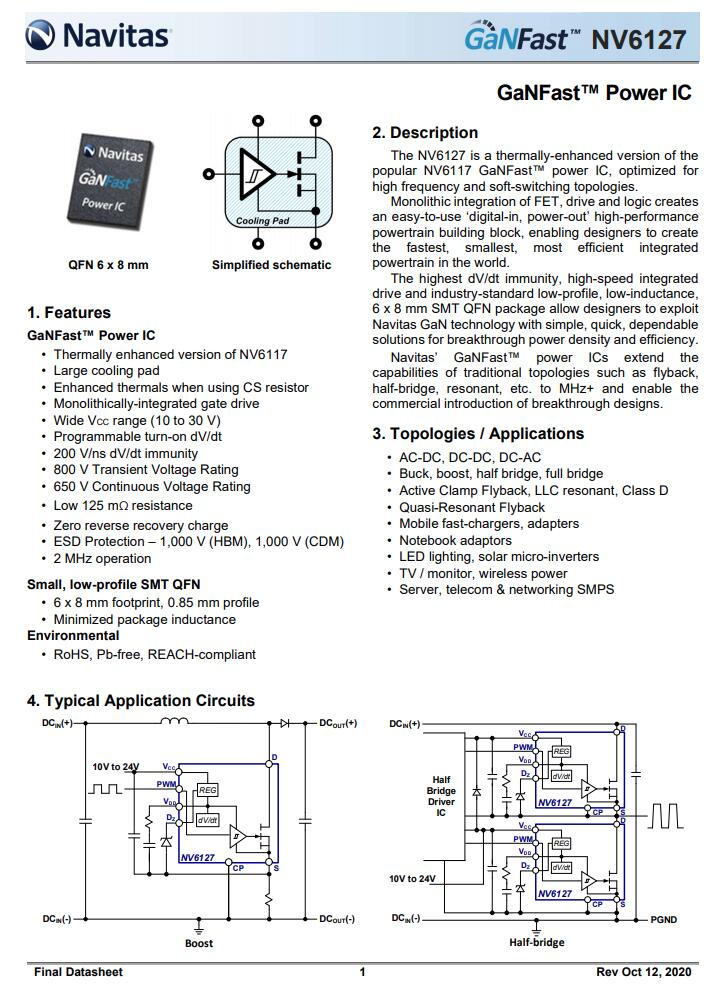
ChargerLAB found that Lenovo 90W flash charging dual-port GaN charger, Baseus 120W GaN plus silicon carbide PD charger also use Navitas NV6127 GaN IC. In addition, Navitas GaNFast power IC has been used by OPPO 50W mini GaN Fast Charger, RAVPOWER 65W GaN Fast Charger, Xiaomi 65W GaN Charger, SlimQ 65W GaN Fast Charger, Anker PowerCore Fusion PD Super Extreme Charger, RAVPower 45W GaN PD charger, Baseus 65W GaN charger and other products, and have been highly praised by the market.
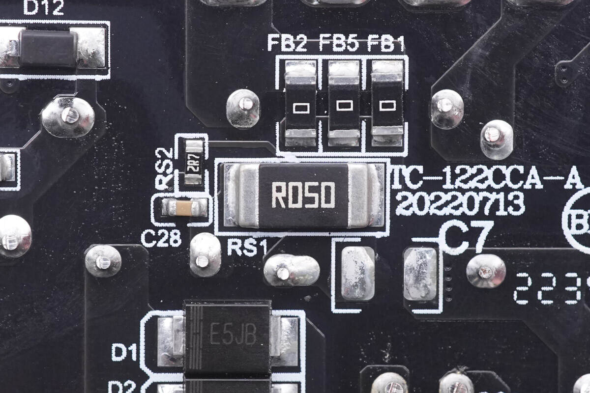
This is the sampling resistor, used to detect the current of the PFC circuit. It adopts 2512 package, and the resistance is 50mΩ.
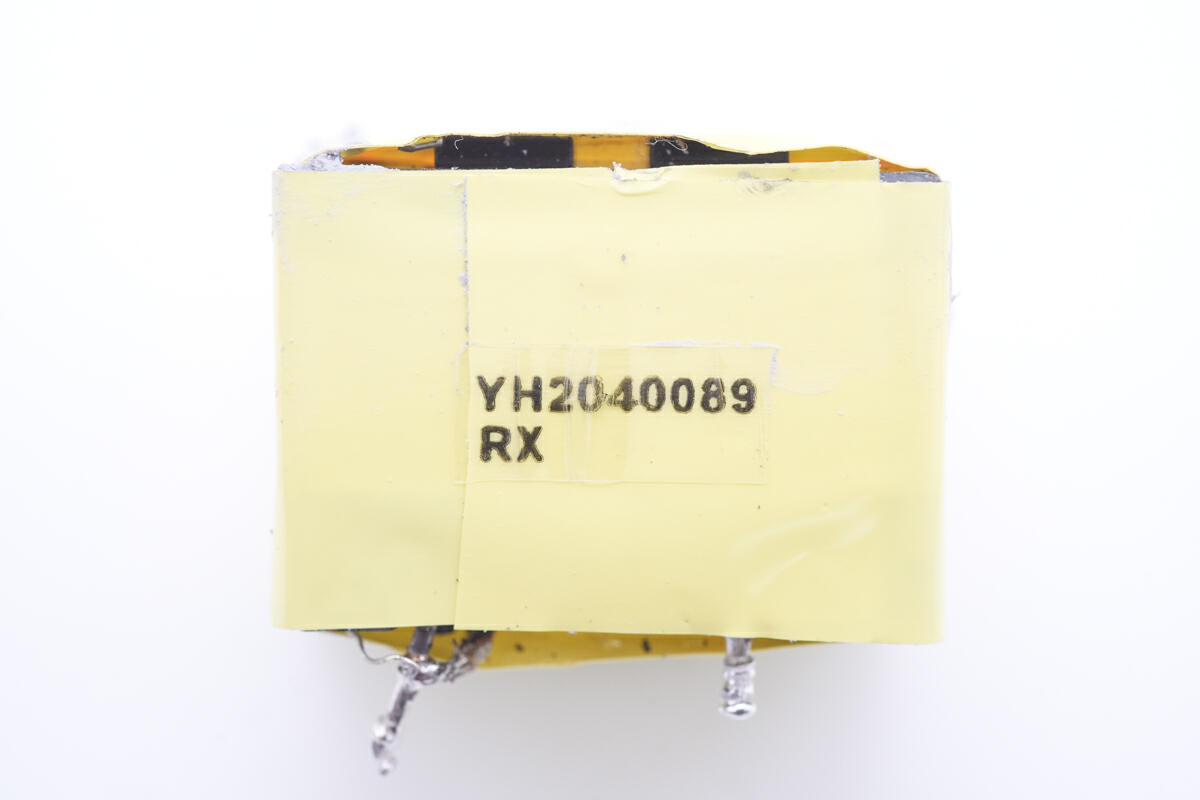
The PFC boost inductor is tightly wound and insulated with yellow tape.
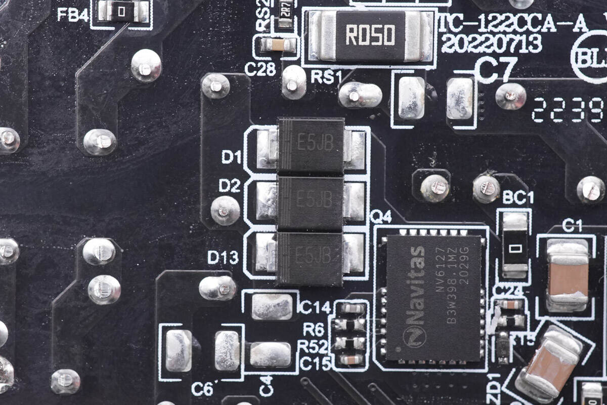
The PFC boost rectifier consists of three ultra-fast recovery diodes.
They are connected in parallel and marked with E5JB. 600V 5A.
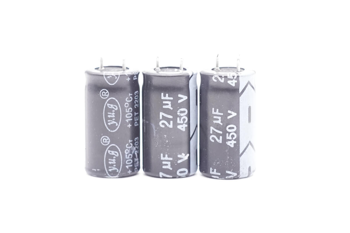
Those three electrolytic capacitors for input filtering are from Yuguang Electronics. 27μF 450V.
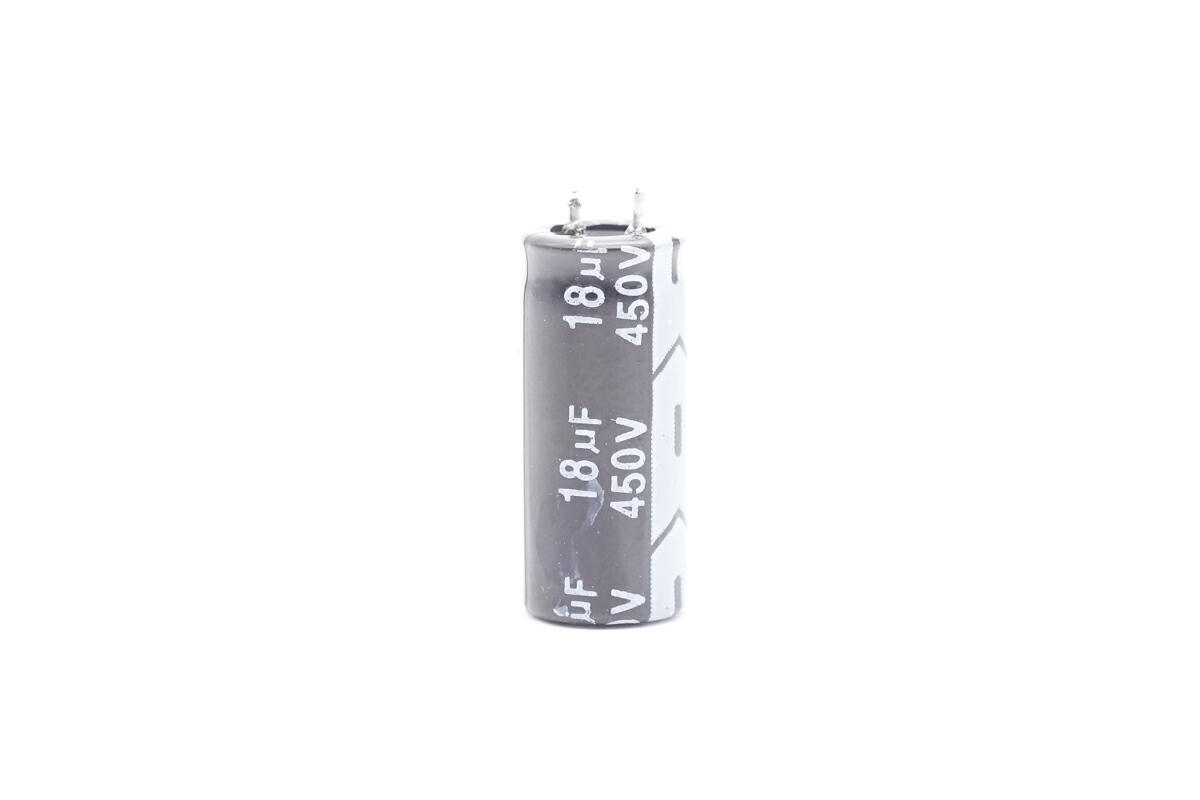
The other electrolytic capacitor is also from Yuguang Electronics.
18μF 450V. And 99μF in total.
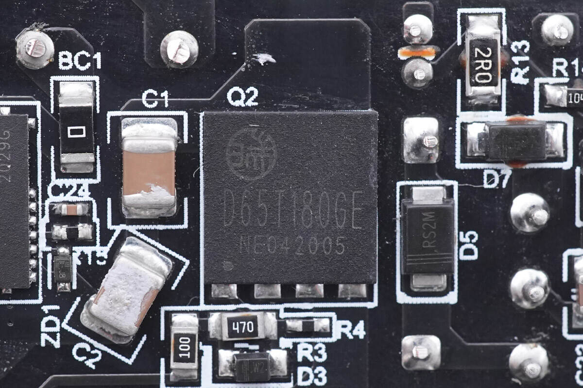
This LLC MOSFET is from HRmicro and adopts DFN8 x 8 package. Model is HRD65T180GE. 700V, 180mΩ.
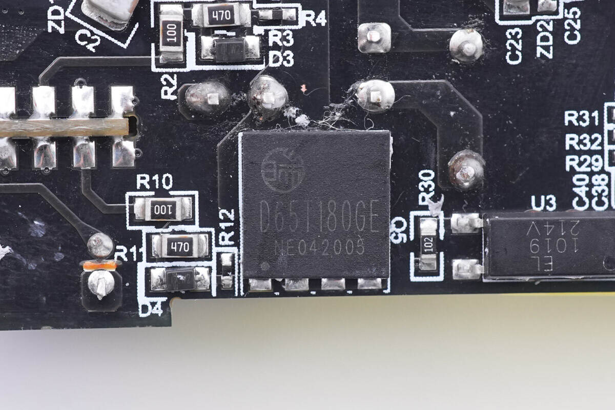
And this is another same MOSFET.
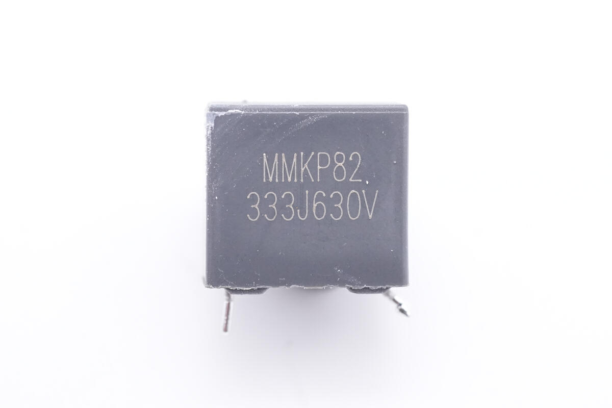
The LLC resonant capacitor is 0.033μF 630V.
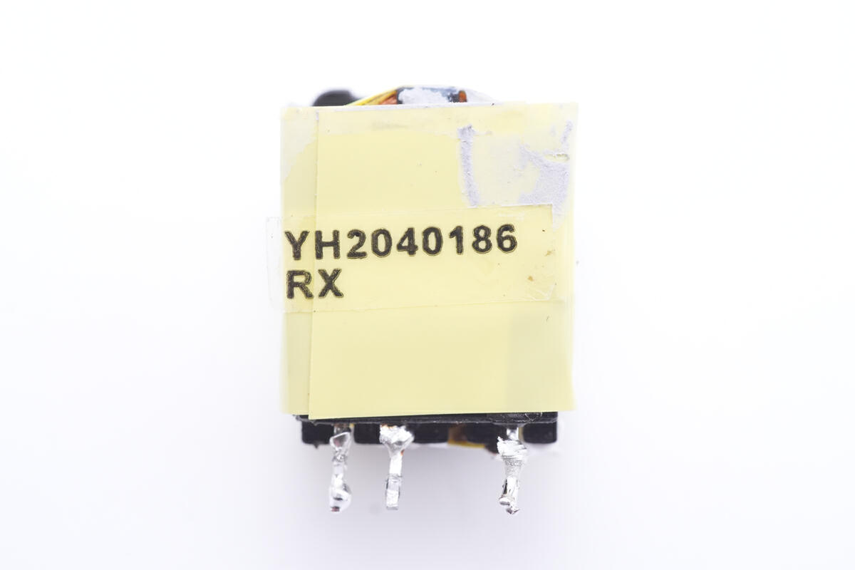
And the resonant inductor is wound with yellow tape.
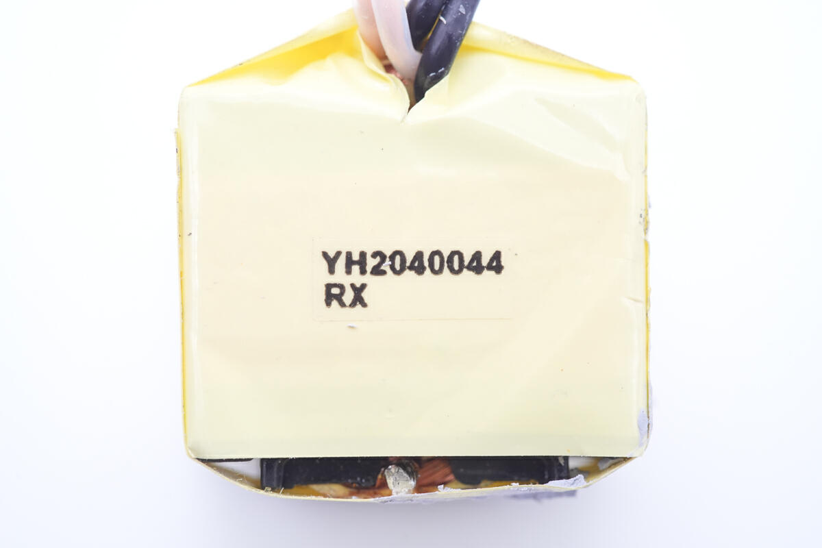
The LLC transformer is also tightly wound with tape for insulation, and the output adopts multi-layer insulated wires.
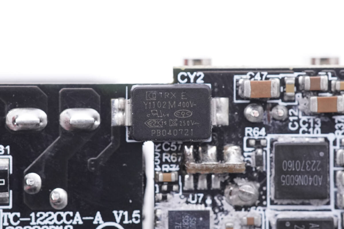
The SMD Y capacitor marked with TMY1102M is from TRX, which features in small size and light weight, and are very suitable for high-density power supply products such as GaN charger.
Teruixiang focuses on the R&D, production and sales of passive components, with a registered capital of 100 million yuan. It has two types of capacitor brands: SMD TRX and DIP TY capacitors. TRX will devote itself to the research of ceramic materials in order to provide customers with more solutions.
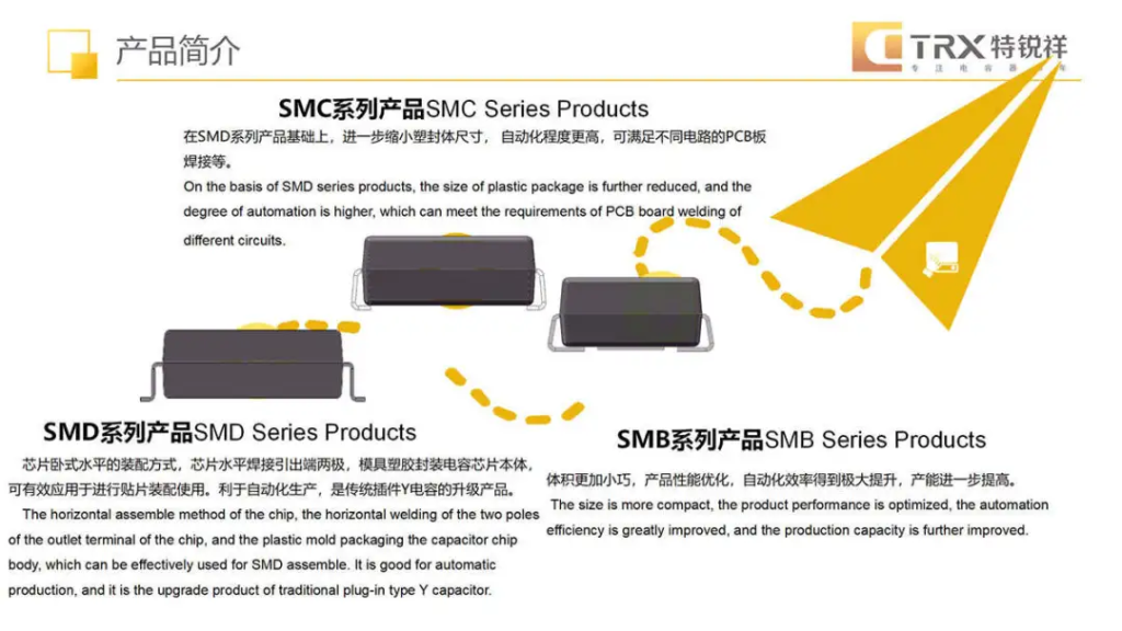
ChargerLAB found that Baseus Qualcomm QC5 certified 100W GaN fast charger, Mcdodo 100W GaN charger, OPPO 65W super flash GaN charger, Lenovo 90W GaN fast charger, Nubia 65W GaN charger, Baseus 120W GaN plus silicon carbide PD chargers are using TRX SMD Y capacitor. It can also be used in ARUN, DIVI, Belkin 20W mini fast charger, the performance has been widely recognized by customers.

Another blue Y capacitor is from DGCX.
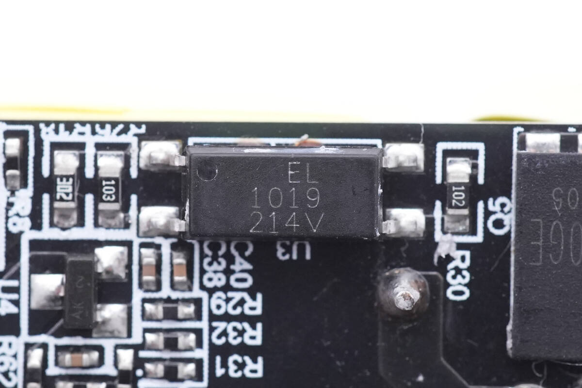
This is the EL1019 optocoupler, used to regulate the output voltage.
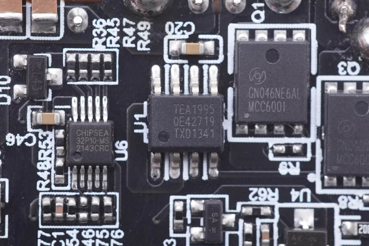
The synchronous rectification controller adopts NXP TEA1995, which integrates two independent drivers for synchronous rectification circuit. It can support 38V working voltage, which can meet the 28V output of USB PD3.1.
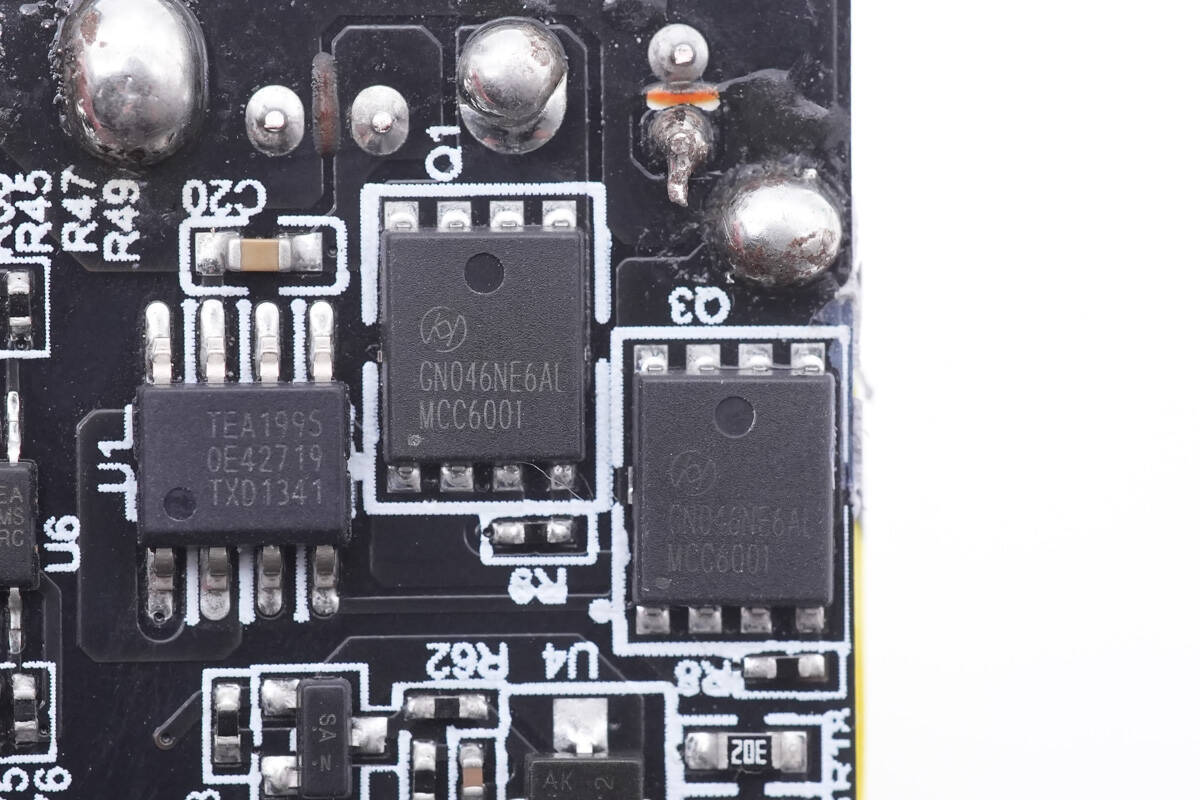
Those two synchronous rectifiers are from Hunteck and adopt DFN5 x 6 package. Model is HGN046NE6AL. 3.8mΩ, 65V.

Those three solid capacitors for output filtering are from Reloncap. 220μF 35V for each.
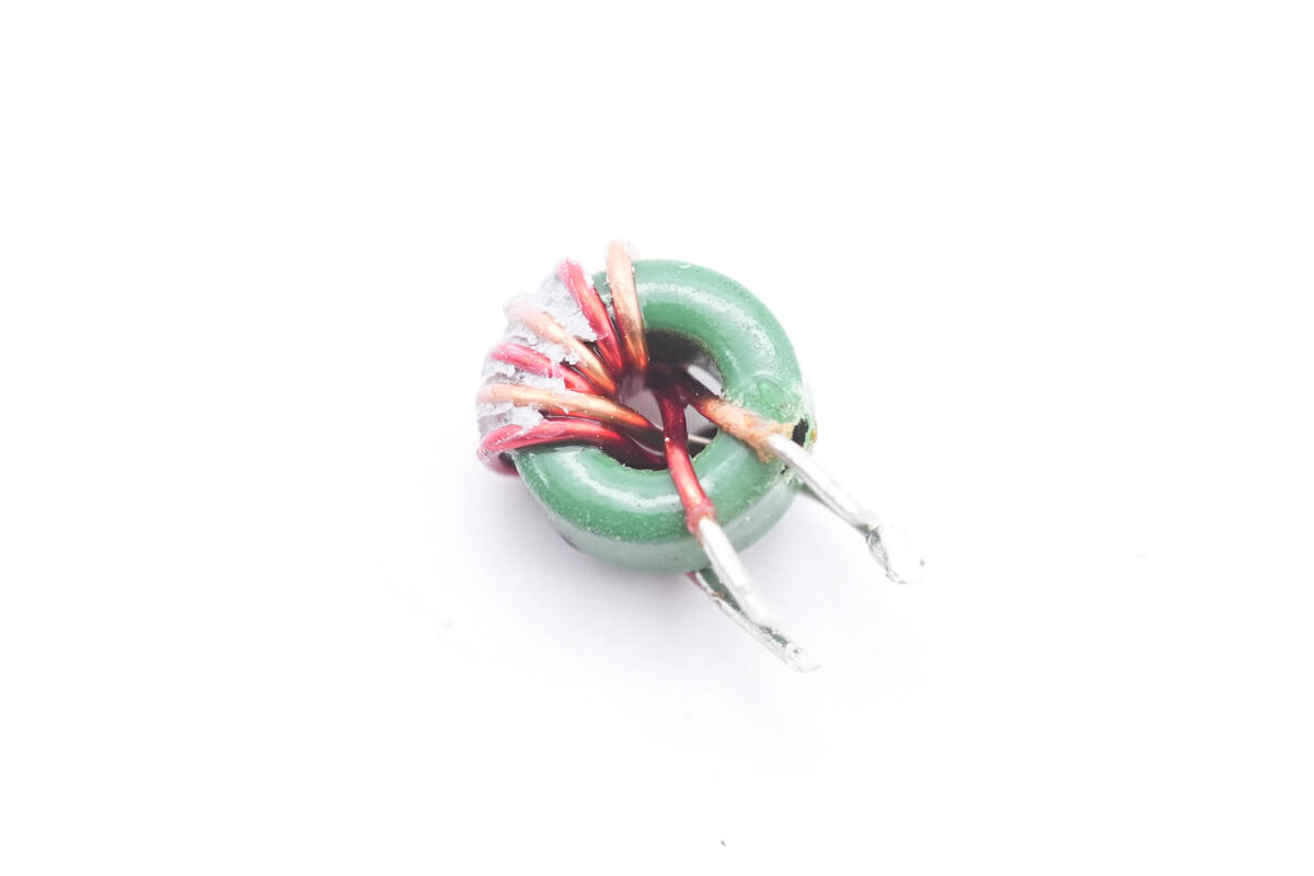
This is the inductor for output filtering.
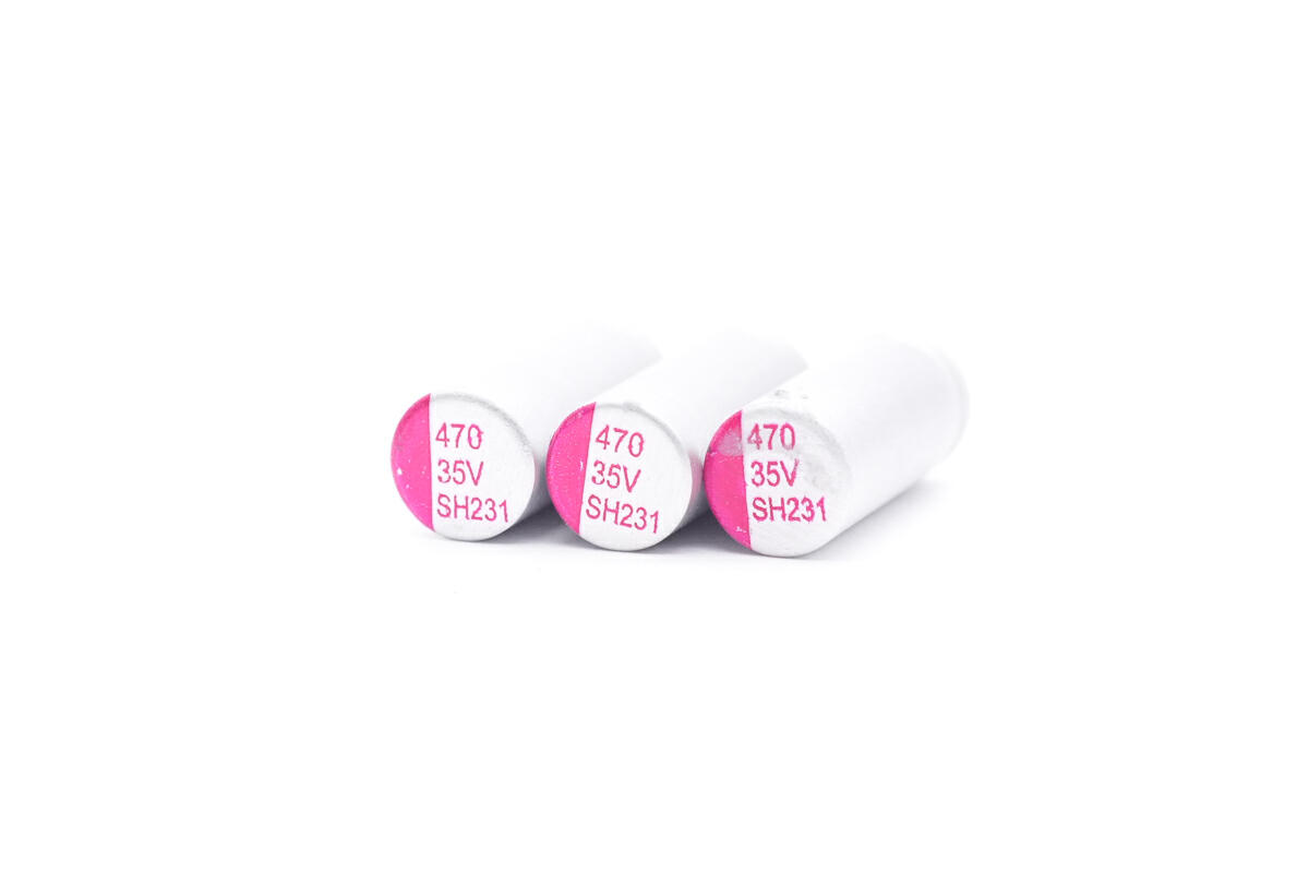
The other three solid capacitors are 470μF 35V.
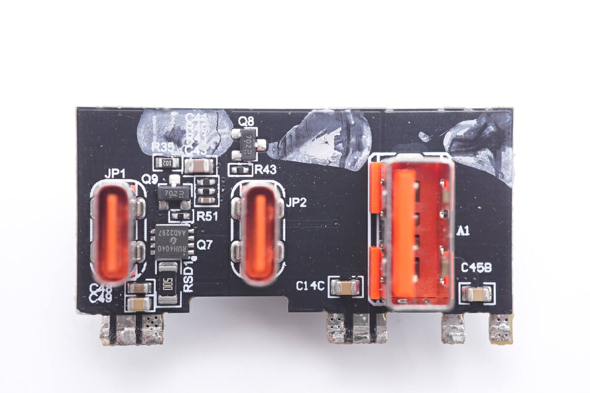
The VBUS MOSFET, USB-C and USB-A sockets are on this output PCB.
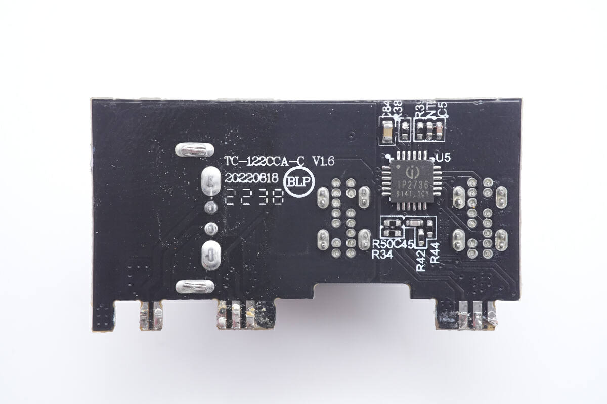
And a protocol chip is one the back.
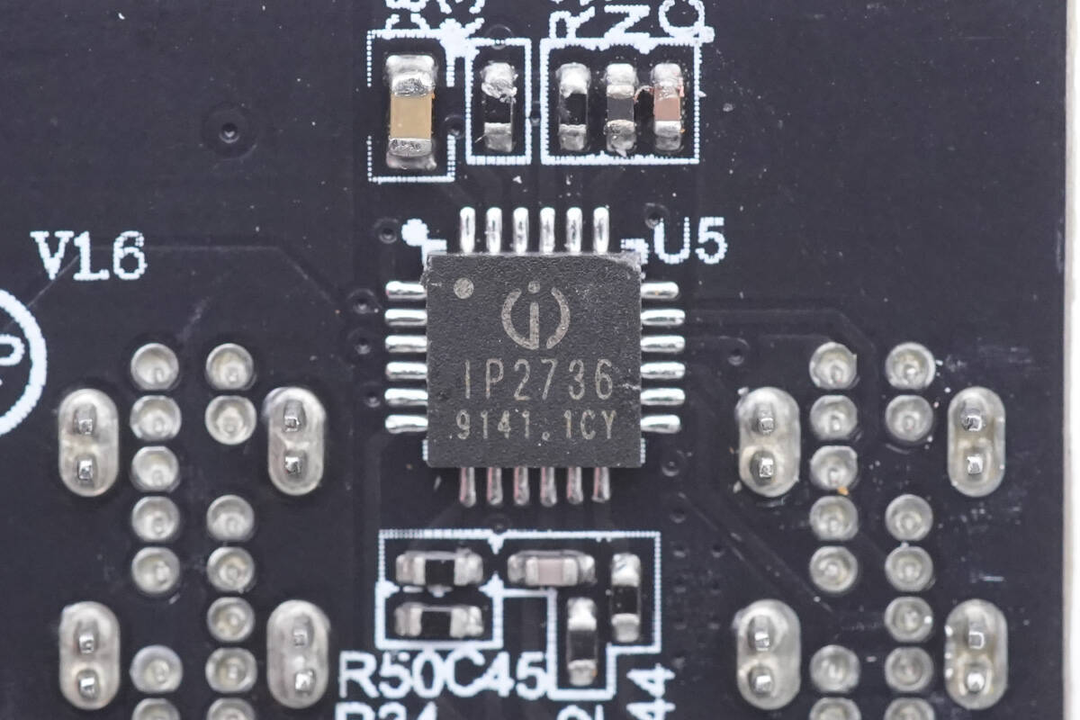
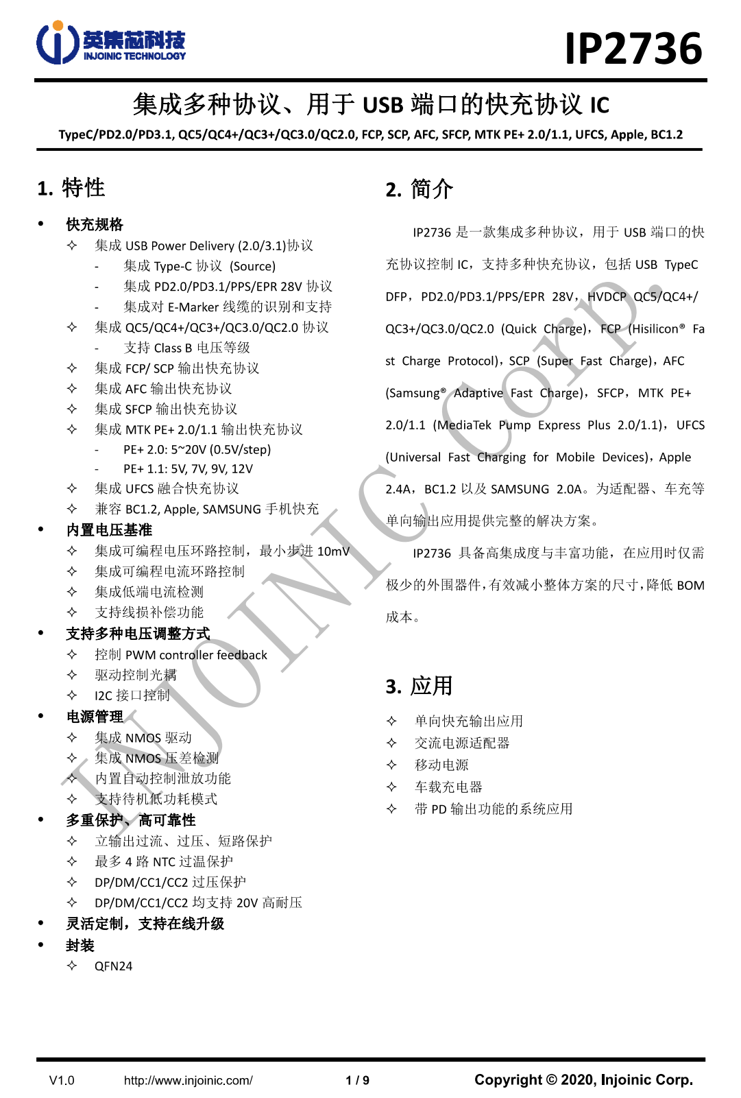
This Injoinic IP2736 protocol chip integrates voltage reference, programmable voltage/current loop control, low-side current detection, and line loss compensation. It also supports optocoupler feedback for power adapter, changes the output voltage through DC-DC controlled by I2C and FB, and is suitable for applications such as car chargers, portable power stations, chargers, power banks, and electric tools.
Thanks to the support of multiple feedback forms, IP2736 can be used with switching power supplies with QR, ACF, LLC and other circuit structures for PD fast charging, and can also be used with high-power car chargers and power banks with buck-boost circuits and other applications.
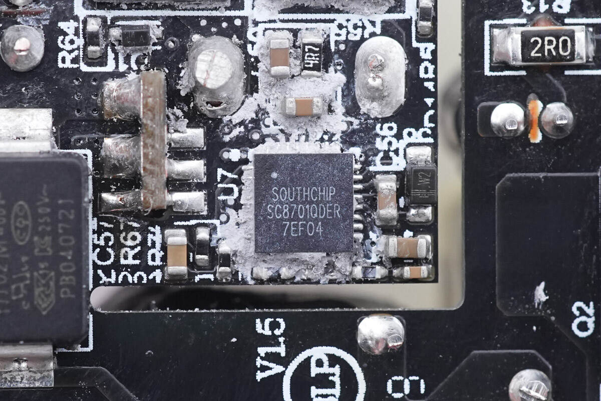
The synchronous buck-boost controller adopts southchip SC8701, which is a 4-switch controller, which supports an input range of 2.7V to 36V and an output range of 2V to 36V. The driver voltage is set to 10V to fully utilize the external MOSFETs for maximum efficiency.
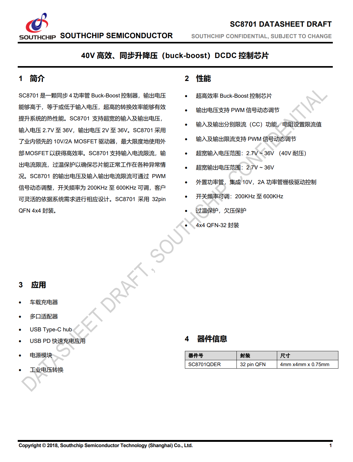
ChargerLAB found that southchip buck-boost chips are widely used in chargers, wireless chargers, power banks, car chargers and other products. The Xiaomi 80W air-cooled wireless charger, Huawei 50W wireless car charger, Anke PowerHouse II 400 portable power station, YOOBAO 300W portable power station, Zimi 200W PD power bank, Zendure SuperTank Pro 100W two-way power bank, Samsung 10000mAh 25W PD power bank and Xiaomi 20000mAh 50W power bank all use their chips.
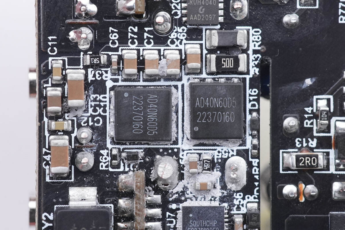
Those two MOSFETs are from Adamant and adopt PPAK 5x6 package. Model is AD40N60D5. 40V, 4.3mΩ for each.
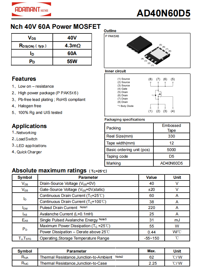
ChargerLAB found that Adamant MOSFET have entered the supply chain of many well-known brands such as Xiaomi, mophie, Meizu, Bull, UGREEN, and Netease, and the product quality has been highly recognized by the market.
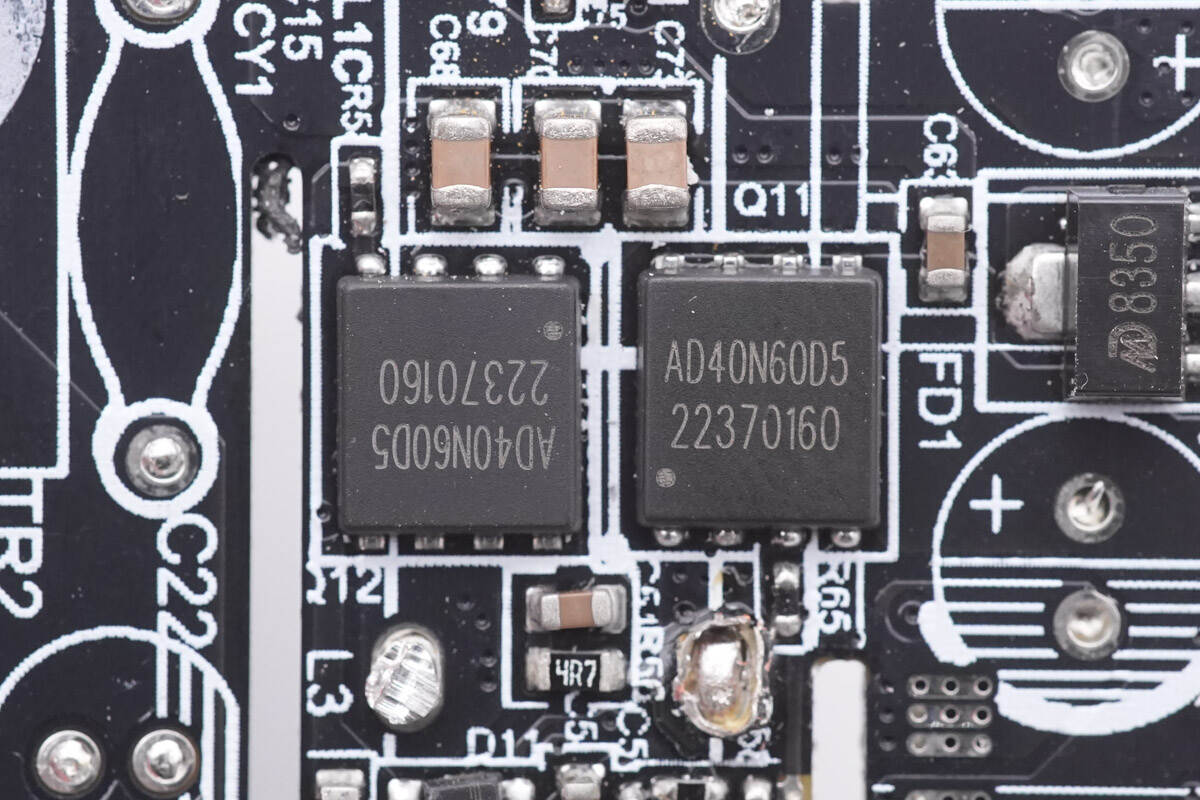
Here are two same MOSFETs.
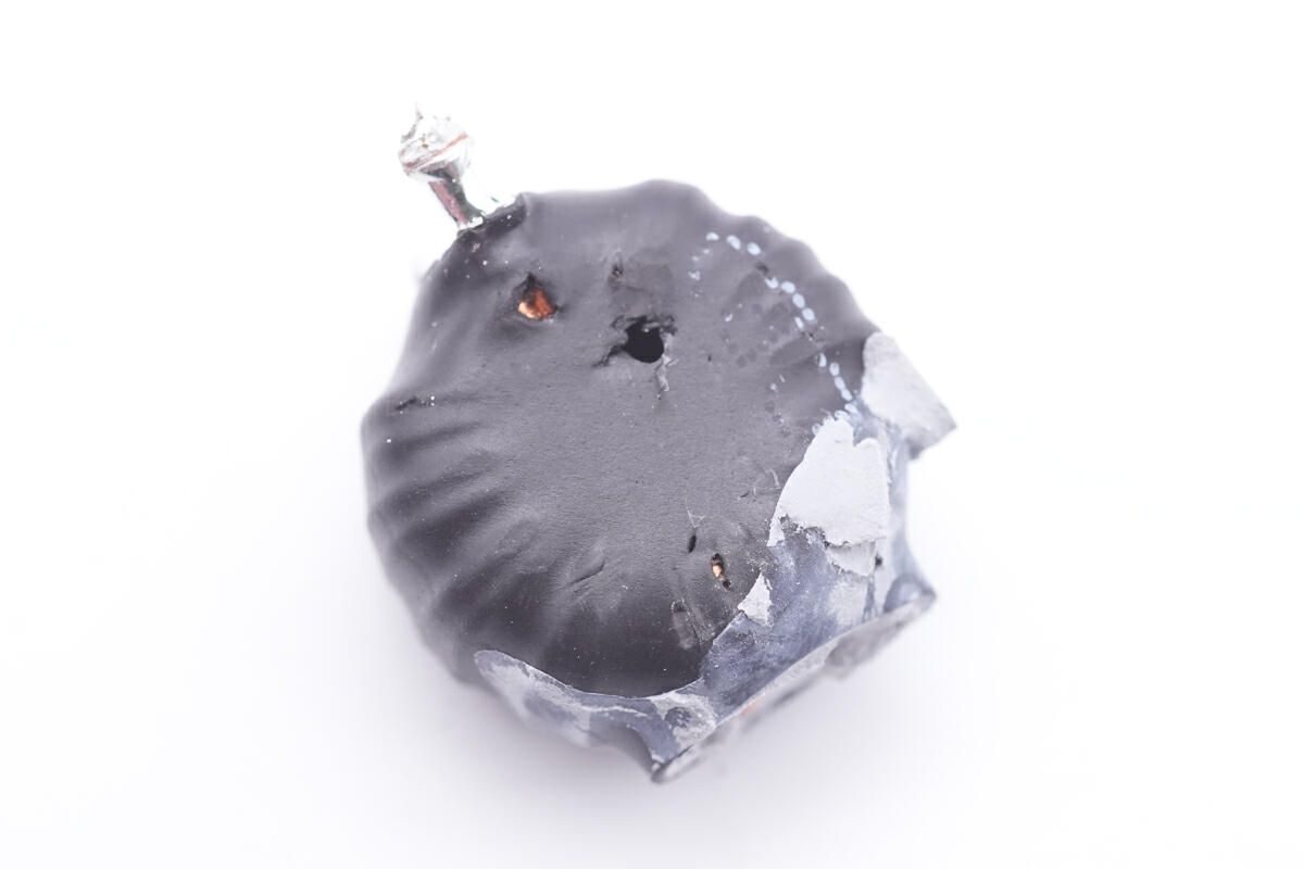
This is the buck-boost inductor, which is insulated with a heat-shrinkable tubing and fixed with silicone adhesives.
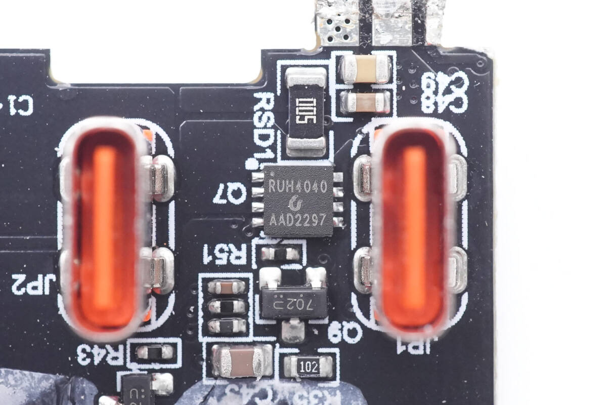
The input VBUS MOSFET is from ruichips and adopts PDFN3333 package. Model is RUH4040M2. 40V 5.5mΩ.
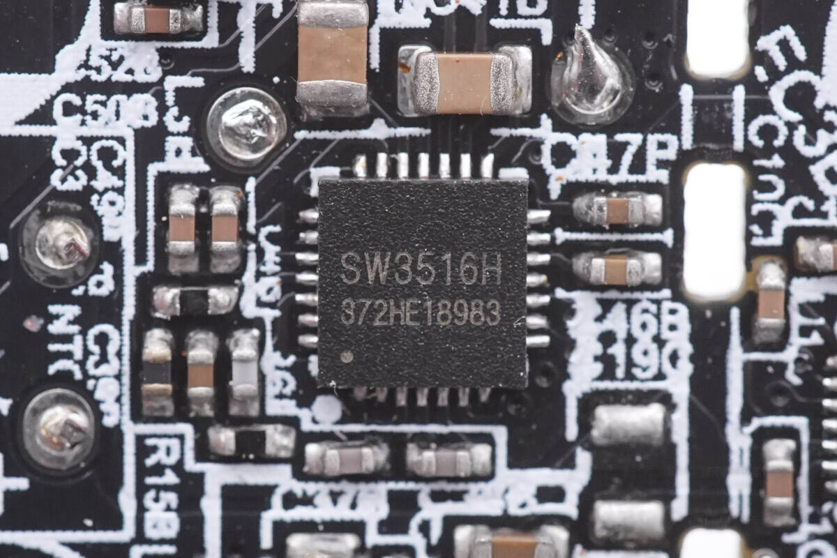
The master control chip of the 100W USB-C port and USB-A port buck circuit adopts Ismartware SW3516H, which is used for buck control and protocol identification. It is a highly integrated multi-protocol charging chip, supports USB-A plus USB-C port fast charging output, and supports dual-port independent current limiting.
It integrates a 5A high efficiency synchronous buck converter, which support PPS, PD, QC, AFC, FCP, SCP, PE and SFCP protocols, dual-port management logic.And the maximum PD output is 100W. It only needs a small number of components to form a complete high-performance multi-protocol dual-port charging solution.
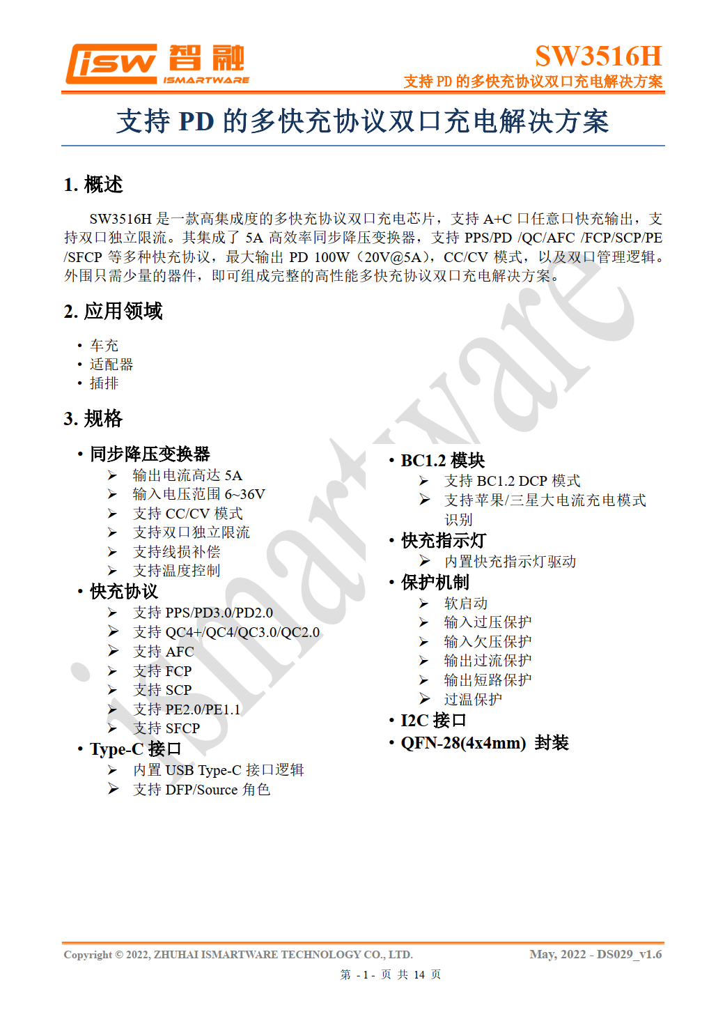
ChargerLAB found that ASUS 65W GaN charger, Nubia 65W three-port GaN charger, Rapoo 65W GaN charger, UGREEN 65W 4-in-1 GaN charger, Lenovo 90W dual-port GaN charger, HUNDA 120W four-port charger and other products also use SW3516H. In addition, Ismartware's fast charging chip can also be used for USB PD power banks, car chargers, etc.
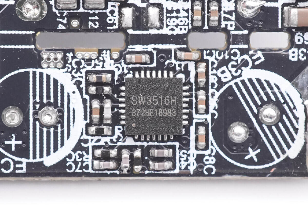
And here is another SW3516H.
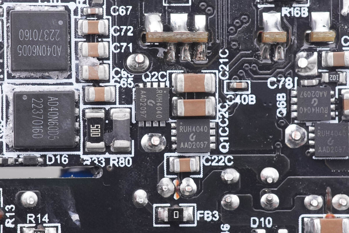
And these two buck MOSFETs are from ruichips. Model is RUH4040M2.
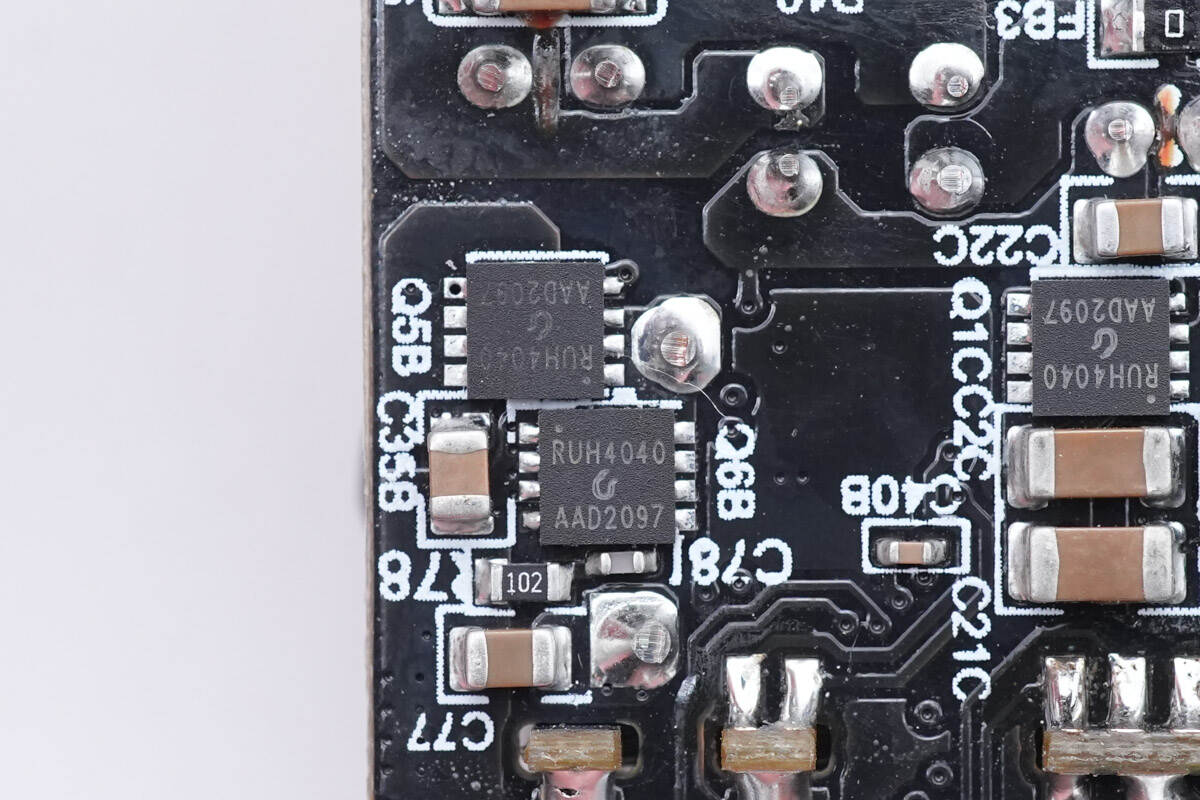
The other two buck MOSFETs are the same.
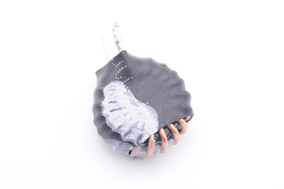
The buck inductor is insulated by heat shrinkable tubing.
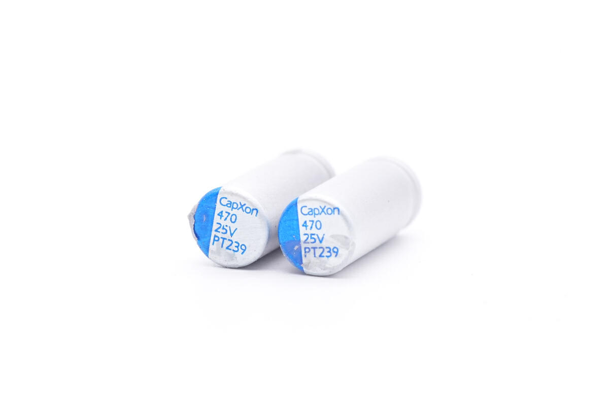
Those two blue solid capacitors are from CapXon PT series, used for output filtering of USB-C2 and USB-A, respectively. 470μF 25V for each.
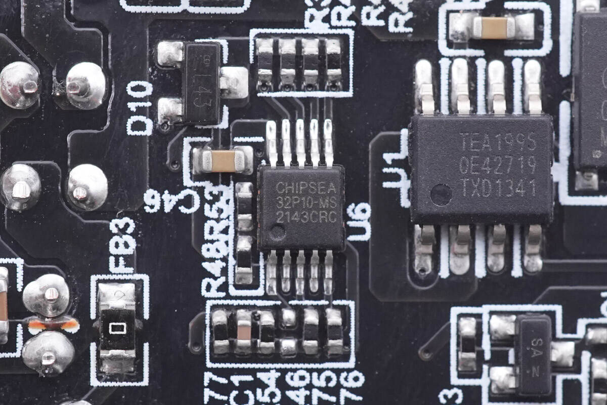
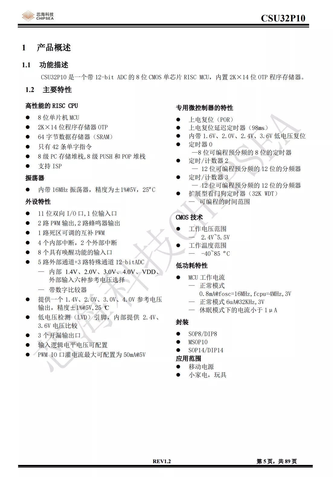
This 8-bit MCU is from Chipsea and adopts MSOP10 package. It integrates 12-bit ADC and is used to control the output power automatically. It also integrates an oscillator and supports 2.4-5.5V working voltage. The model is CSU32P10
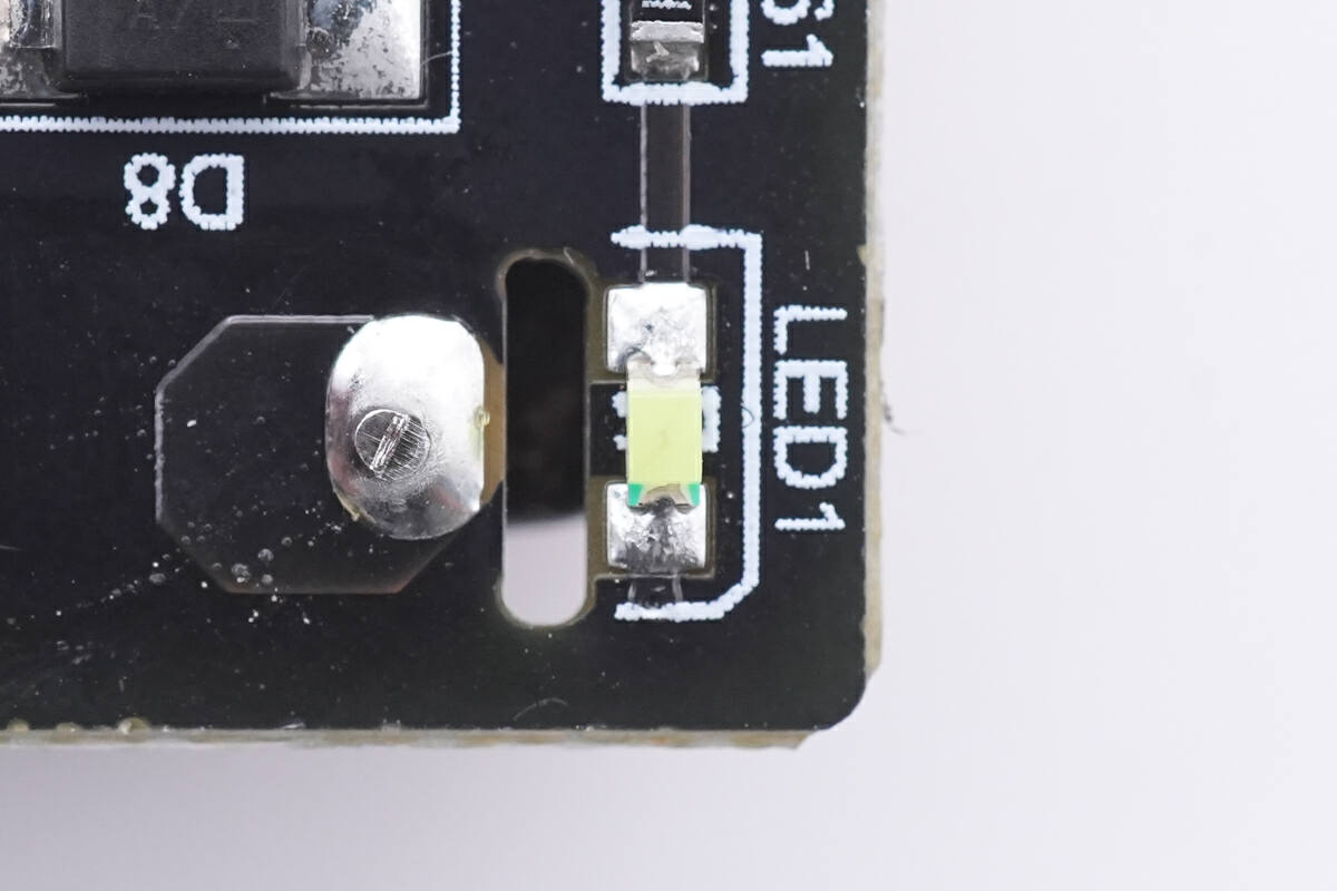
This is the LED power indicator.
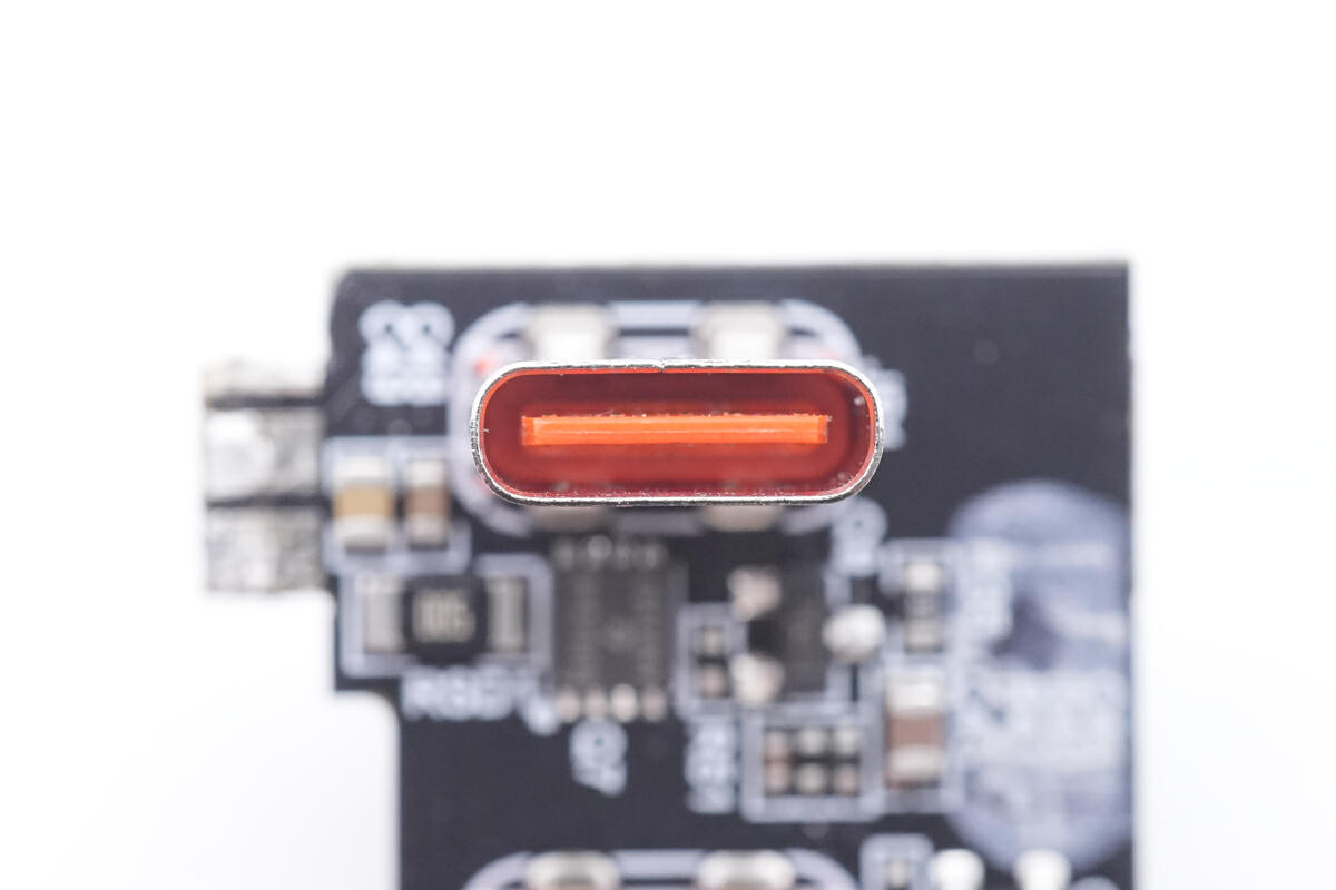
The plastic sheet inside the USB-C socket is orange.
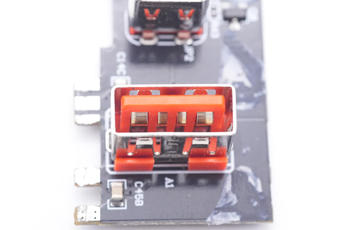
And the plastic sheet inside the USB-A socket is also orange.
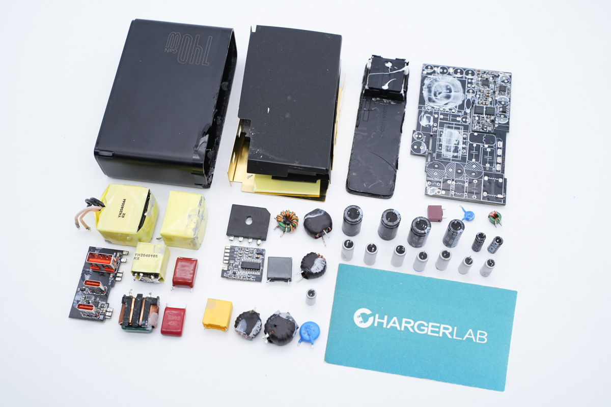
That's all for the teardown.
Summary of ChargerLAB
Well, that's all components of this 140W PD3.1 charger from Baseus. The USB-C1 can support up to 140W and has almost the same size as the Apple 140W. But unlike the Apple 140W, it has an extra USB-C and USB-A port. So, you can fast charge multiple devices at once.
After taking it apart, the internal layout is pretty compact. Multiple small vertical PCBs can significantly reduce the charger's size. It has two-way independent output circuits, used for USB-C1 and USB-C2, USB-A, respectively.
This product is priced at $89.99. You can click the button at the beginning or the end of the article to get one.
Related Articles:
1. Teardown of Baseus 100W Slim Laptop Power Bank (Blade Series)
2. With USB-C Cable | Teardown of Baseus 65W Elf Power Bank (20000mAh)
3. Teardown of Baseus 20W 10000mAh MagSafe Wireless Power Bank (For iPhone 14/13/12)

