Introduction
In today's age of technology, having multiple gadgets and devices is almost a necessity. However, constantly juggling between charging cords can be a hassle. That's where a power strip with multiple USB ports comes in handy! And today, we got our hands on the Baseus 100W GaN3 Pro Power Strip. With this convenient device, you can charge several devices at once without the need for individual chargers cluttering your countertop or desk. So, let's take a look at the components and structure of this product.
Product Appearance
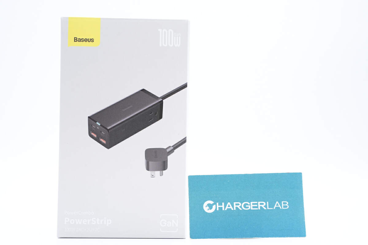
The Baseus 100W GaN3 Pro Power Strip comes in a simple packaging that displays the power and device's appearance.
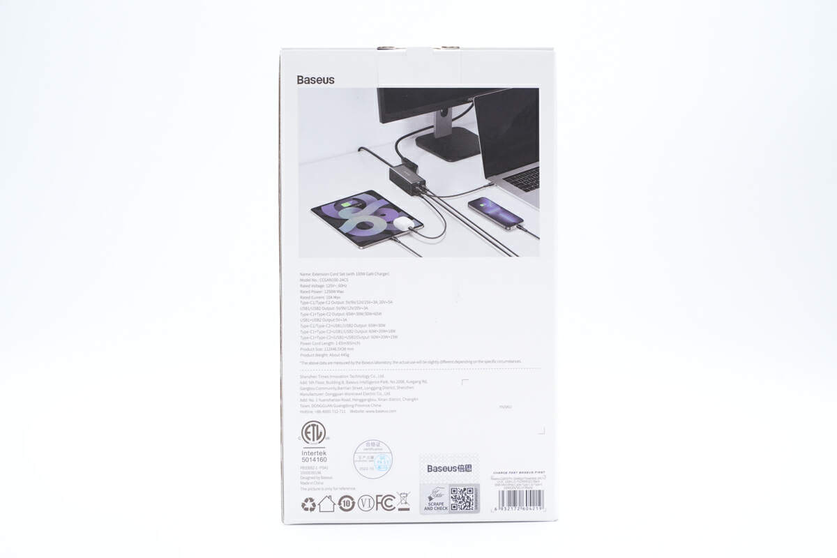
The back of the packaging shows the product's capability of charging laptops, tablets, phones, and headphones simultaneously, along with its specifications.

It contains a power strip, cable, user manual, and warranty card. The power strip comes wrapped in an anti-static dust bag, ensuring the device's safety during transport.
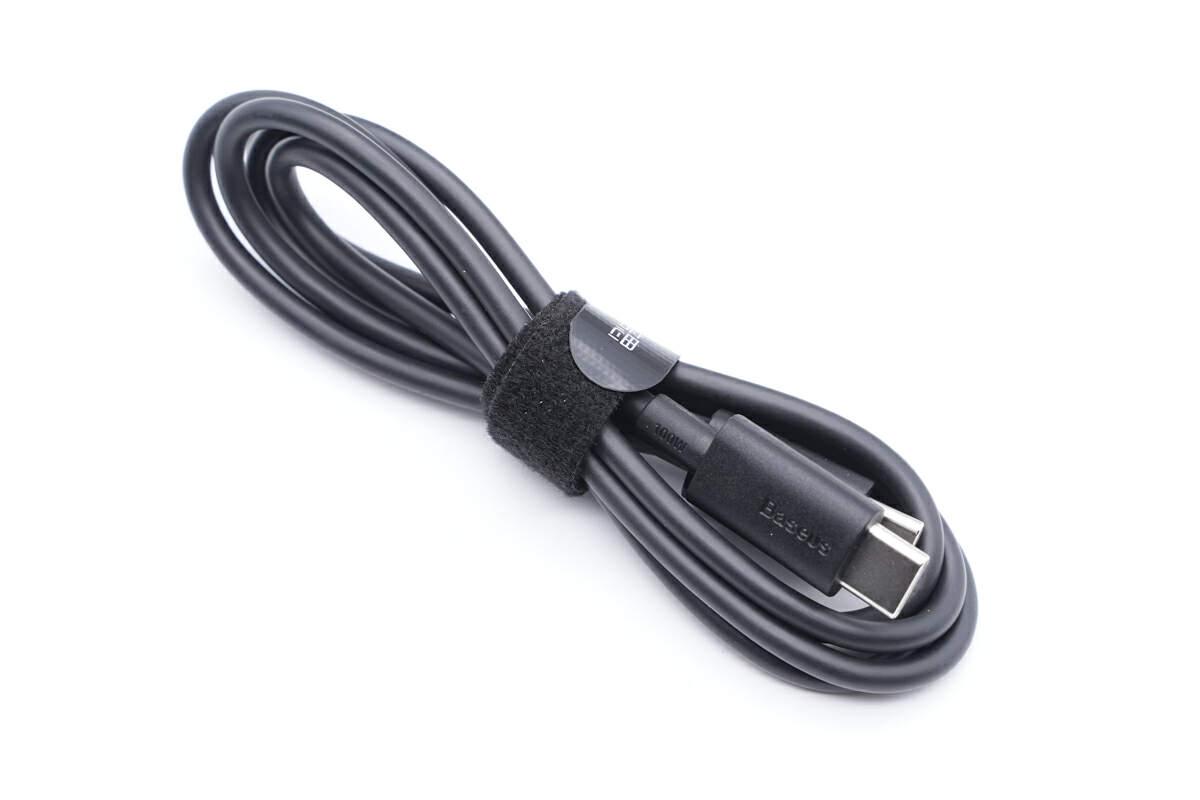
This is a dual USB-C cable, and has a Velcro cable tie for easy organization.
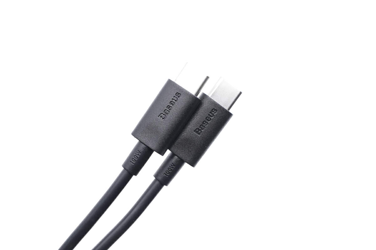
The 100W on the connector means it can support 20V5A 100W fast charging.
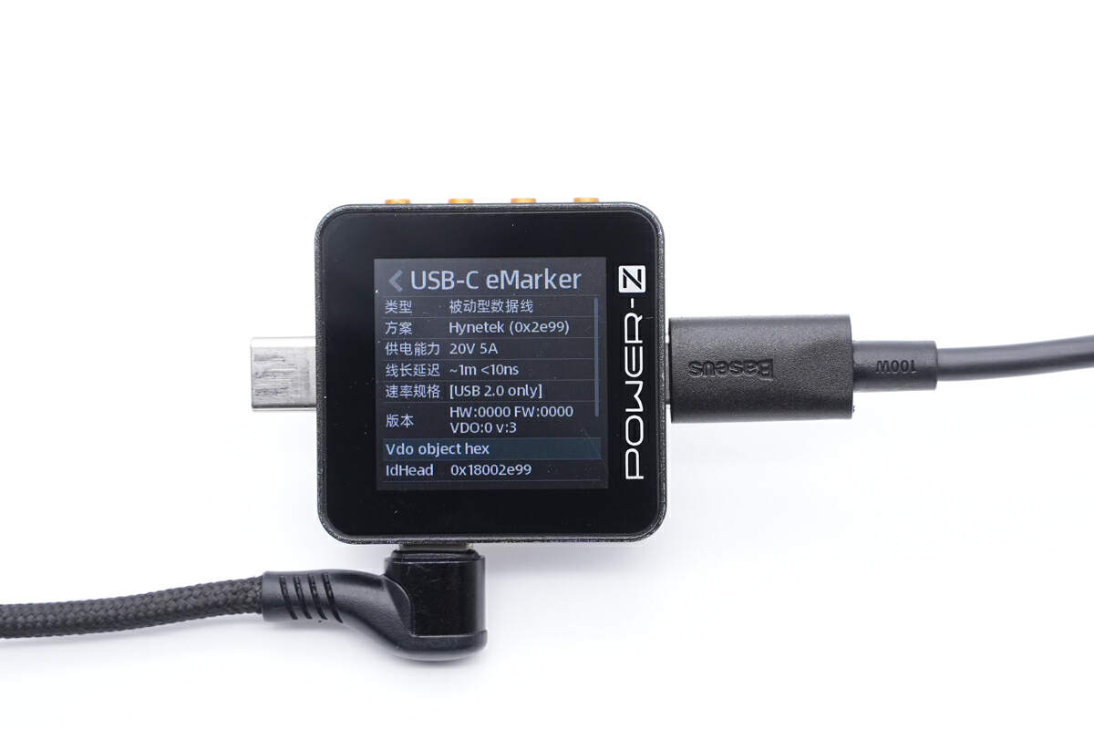
We also confirmed this using ChargerLAB POWER-Z KM002C.
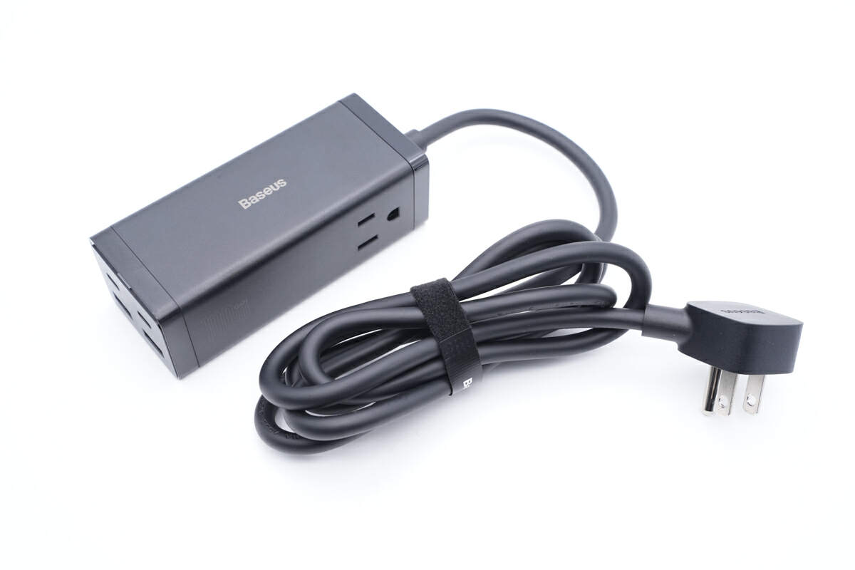
The power strip continues the design of this series with Baseus logo on the side.
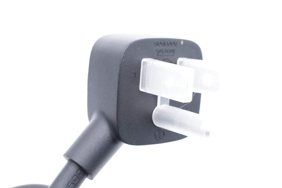
The power cord has a three-prong plug with a plastic cap protection on the prongs.
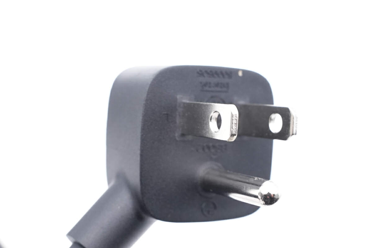
One of the prongs is used for grounding.
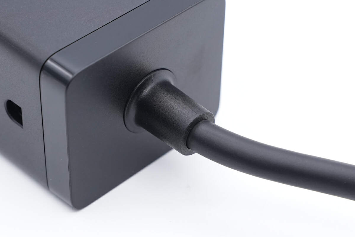
The power cord and body junction come with a rubber sleeve for added protection.
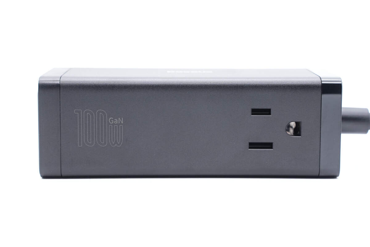
The 100W GaN and a AC outlet are on this side.
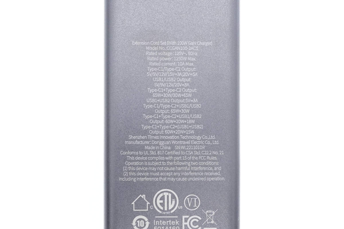
All specs info are on the opposite side. Model is CCGAN100-2ACS. It can support AC input of 125V~60Hz 2.5A. And the rated power is 1250W. As for the DC part, two USB-C ports can support up to 100W. And two USB-A ports can only support up to 60W. The total output power won’t exceed 100W. This power strip has passed FCC, ETL certification.
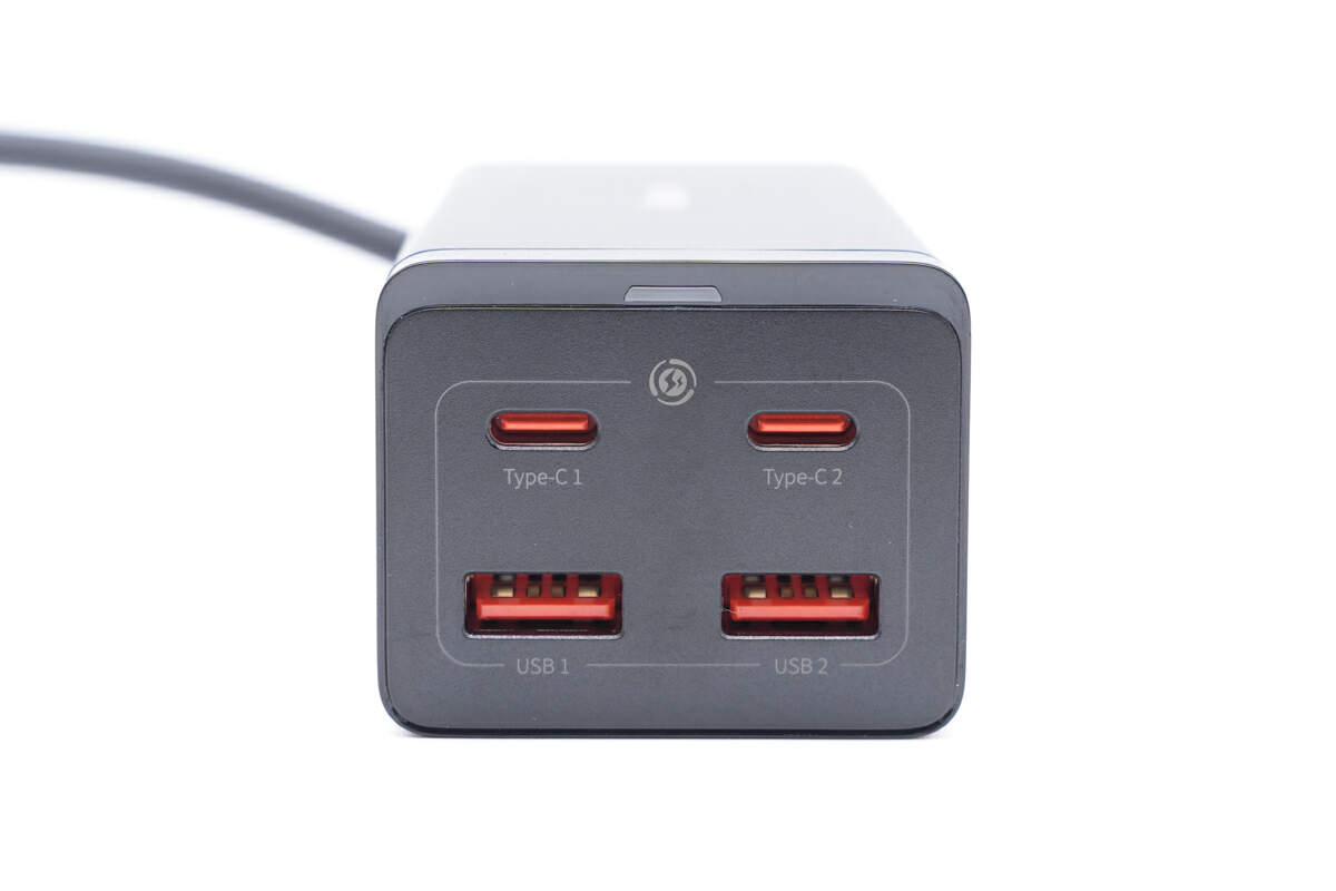
Two USB-C and two USB-A ports are on the output panel, and an indicator light is at the top.
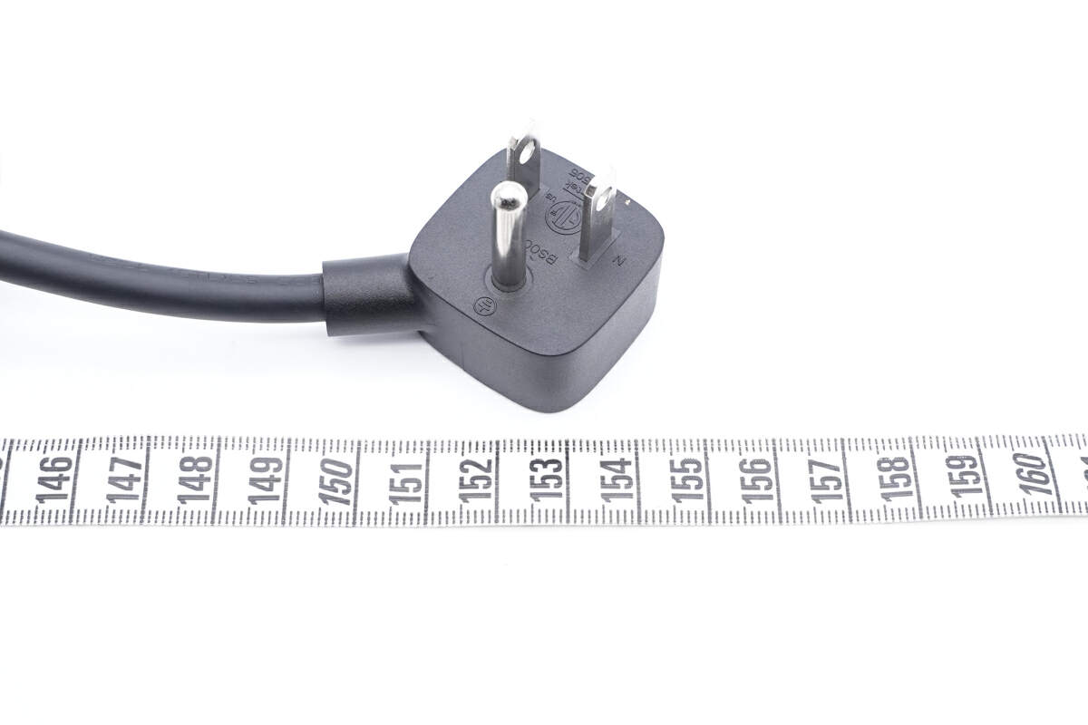
The length of the power cord is about 1.5m (4’ 11”).

The length of the power strip is about 111.6mm (4.39 inches).
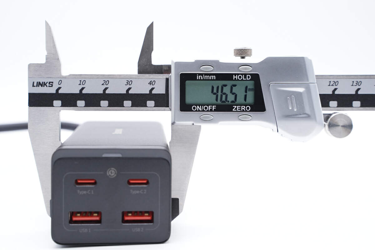
The width is about 46.5mm (1.83 inches).
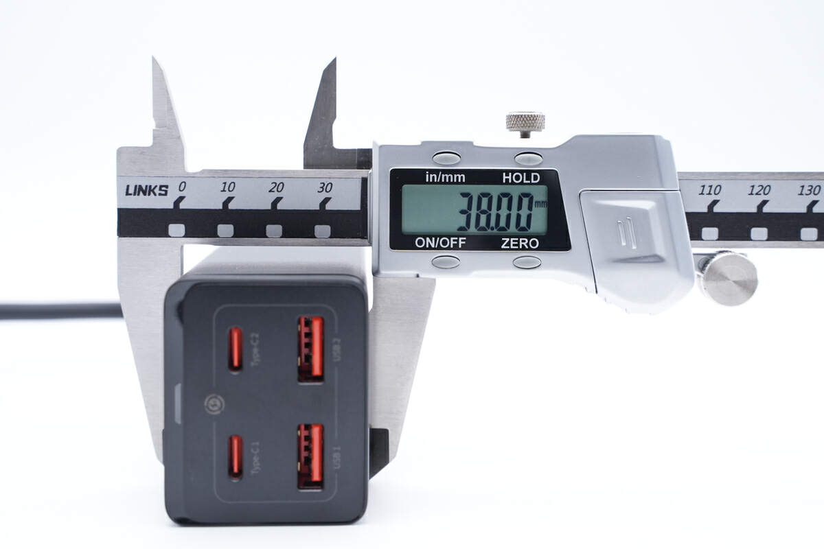
And the height is 38mm (1.5 inches).
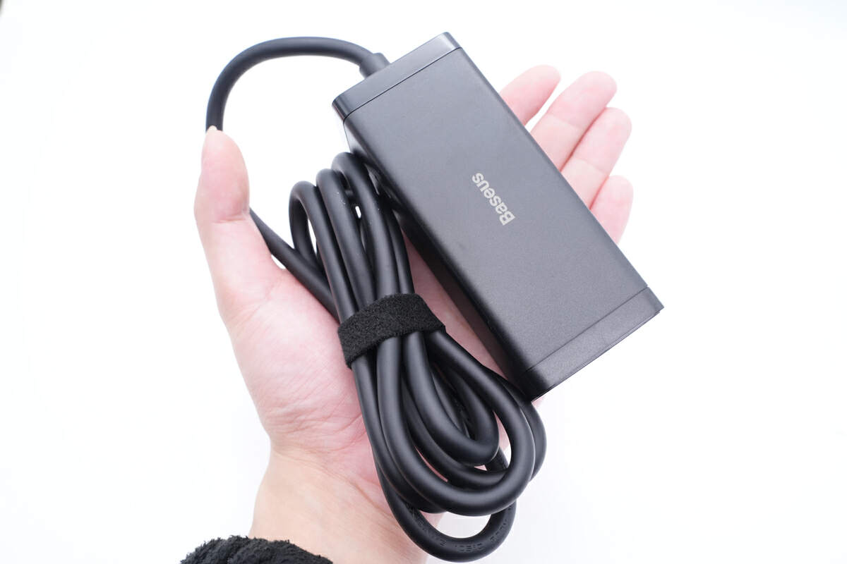
This is how it looks like on my hand.
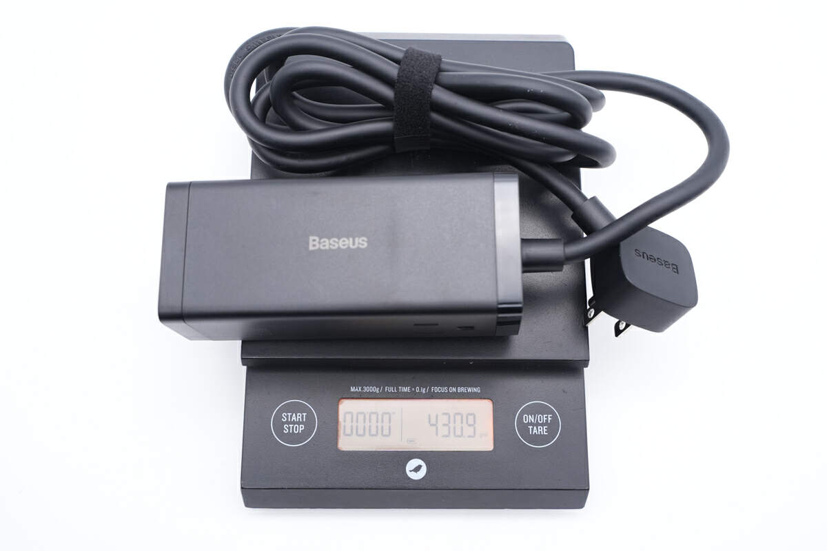
And the weight is about 431g (15.2 oz).
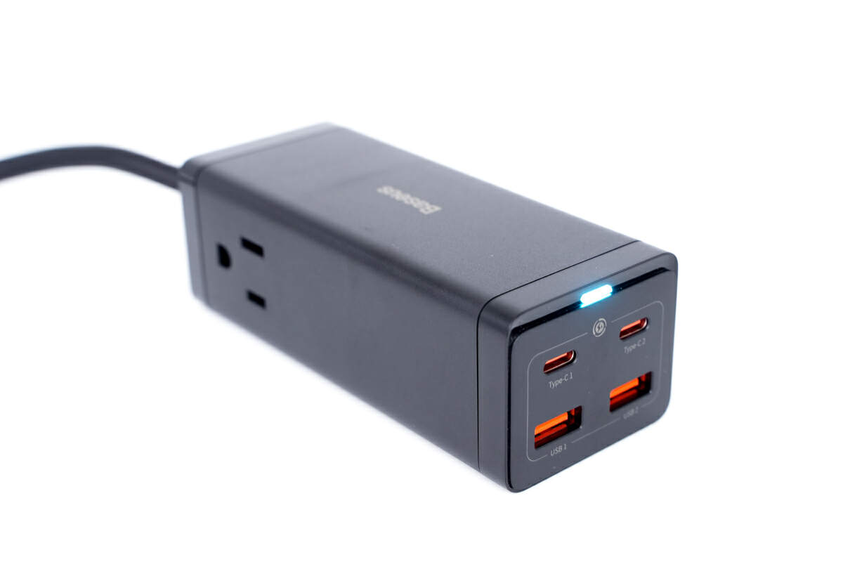
When powered on, the indicator will light up in blue.
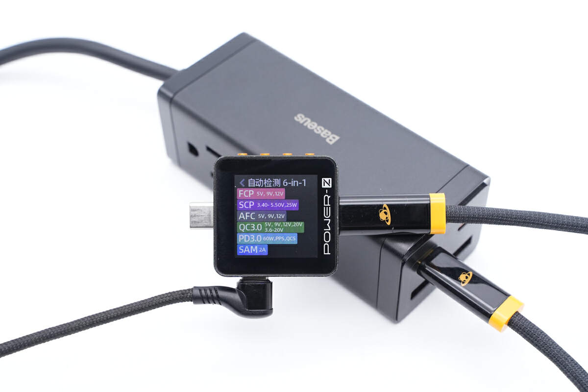
The ChargerLAB POWER-Z KM002C shows the USB-C1 supports FCP, SCP, AFC, QC3.0, PD3.0, PPS, QC5 protocols.
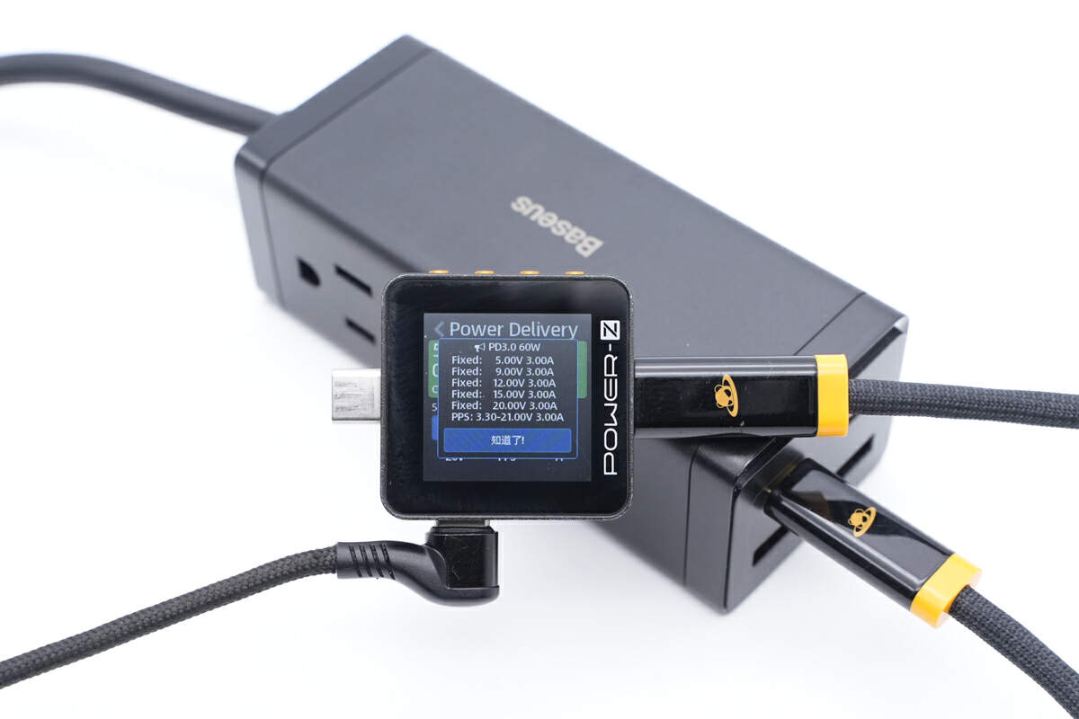
And it also supports five fixed PDOs of 5V3A, 9V3A, 12V3A, 15V3A, 20V5A, and a set of PPS.
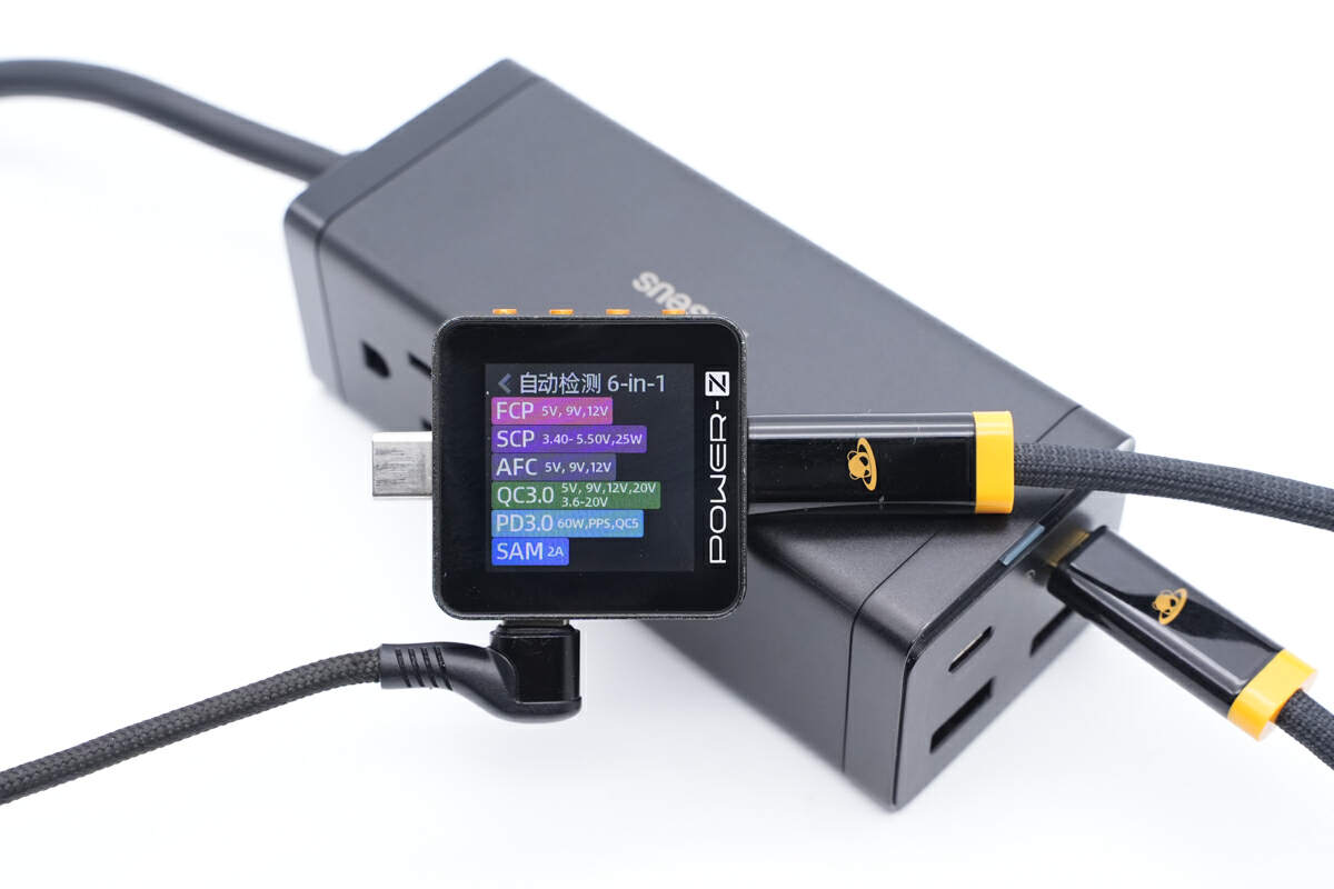
We found the supported protocols of USB-C2 is exactly the same as that of USB-C1.
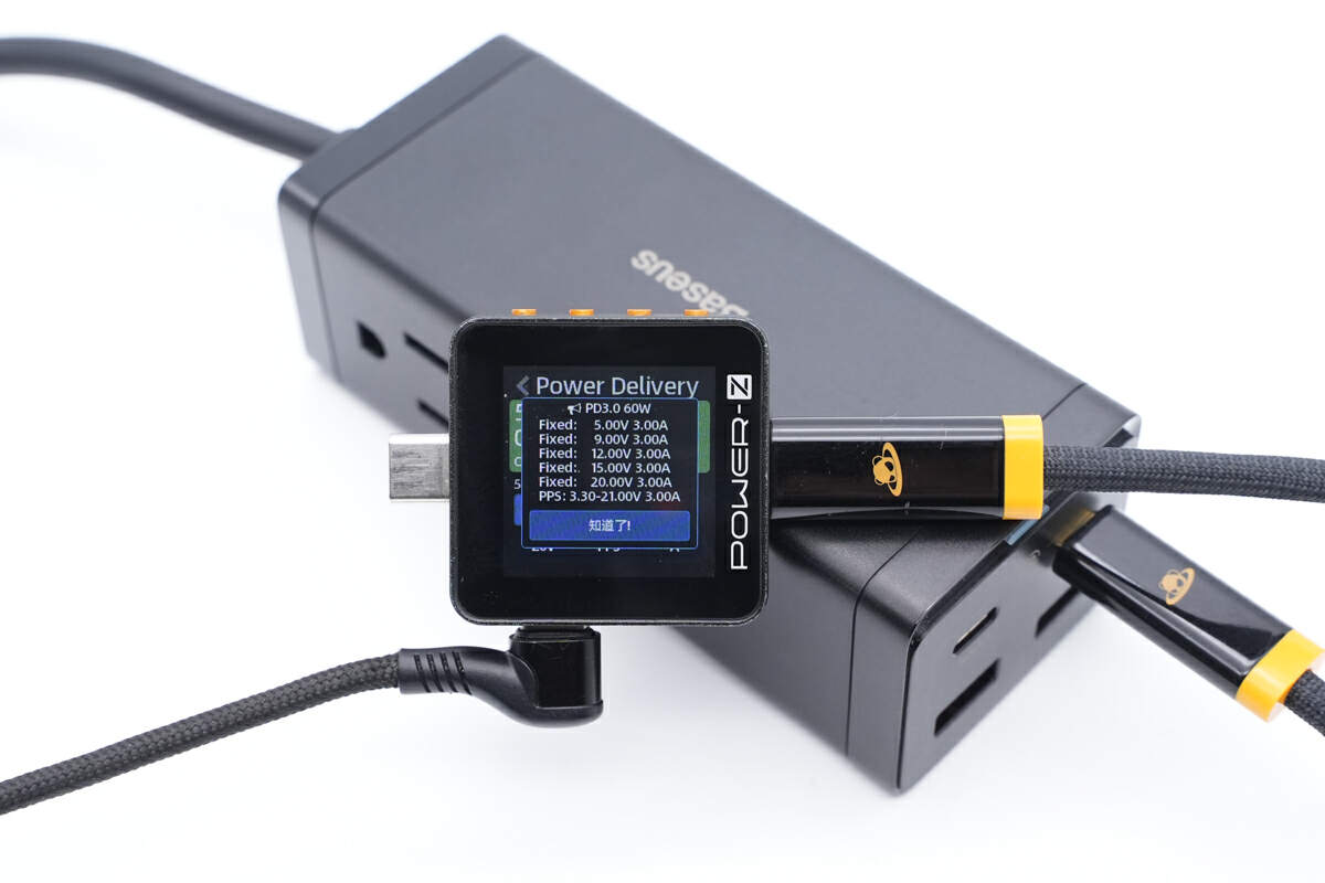
Same goes for the PDO info, so you can use any USB-C port to get the same charging speed.
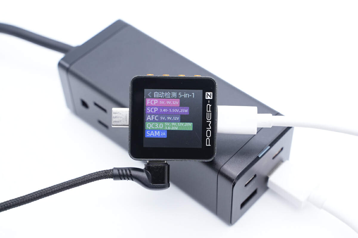
And the USB-A1 supports FCP, SCP, AFC, QC3.0 protocols.
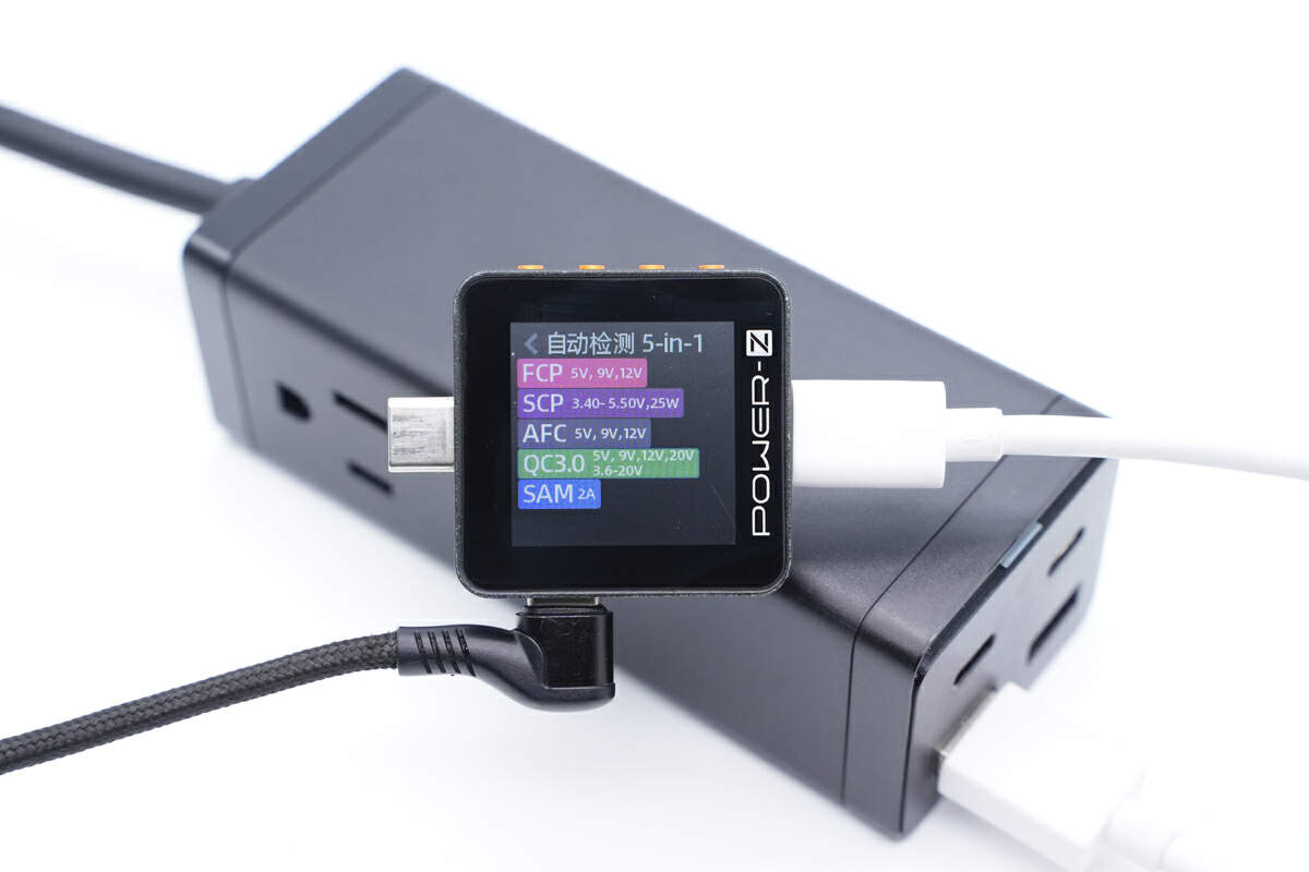
And the other USB-A port is the same.
Teardown
Next, let's take apart the power strip.
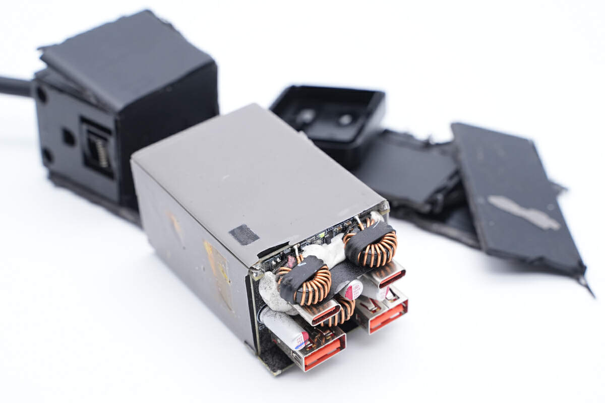
Firstly, use a cutting machine to open the shell and take out the internal PCBA module. It uses potting technology, which not only enhances heat conduction and uniform heat dissipation but also fixes the position of components. This effectively prevents damage to the power strip due to falling.
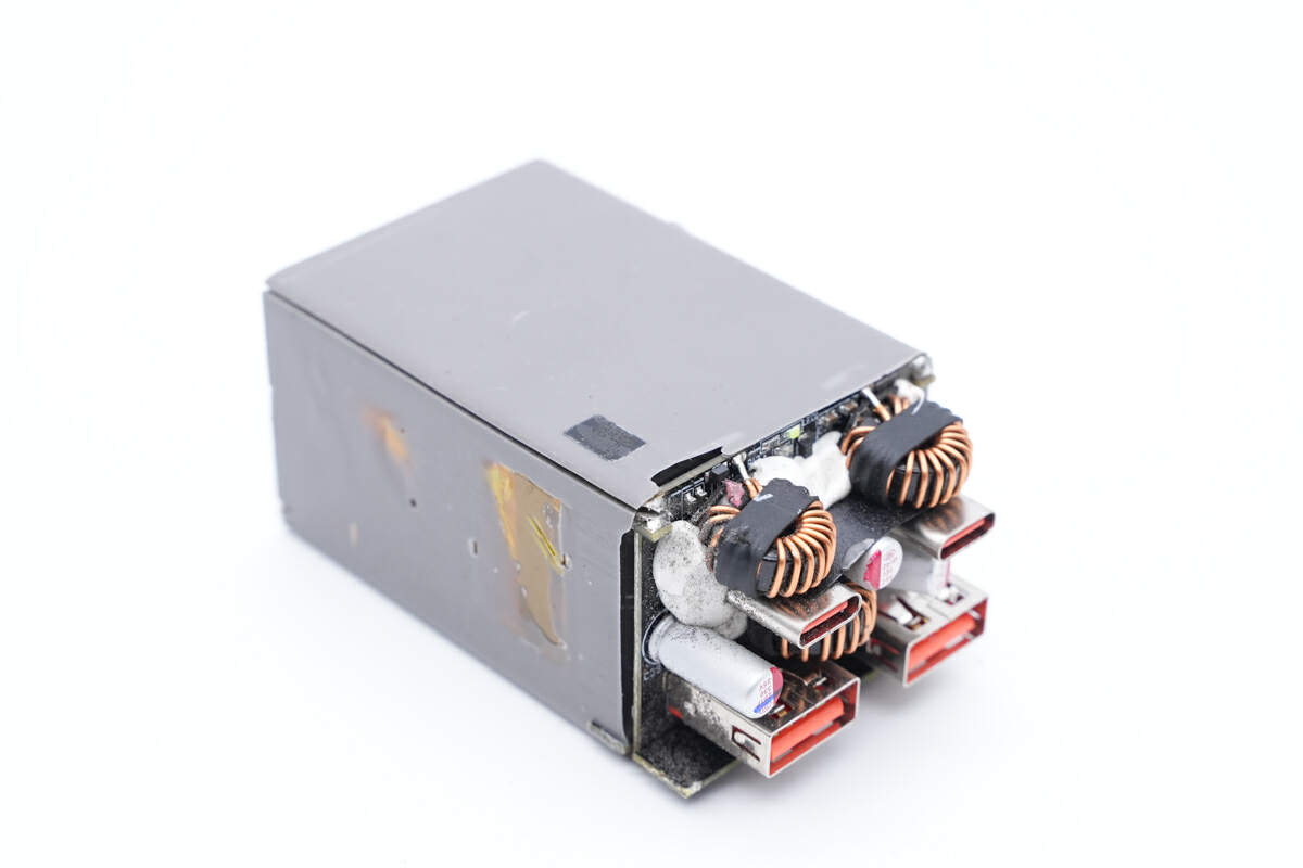
The entire internal PCBA module is potted into a whole, and the buck inductor and USB module are soldered on this small PCB.
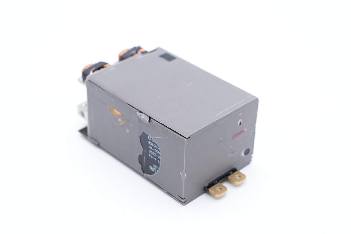
The other end of the PCBA module is the input pin, which is connected to the power supply inside.
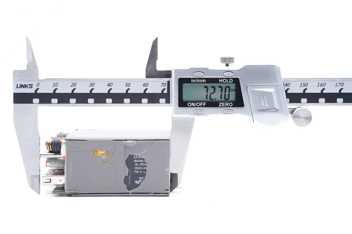
The length of the PCBA is about 73mm (2.87 inches).
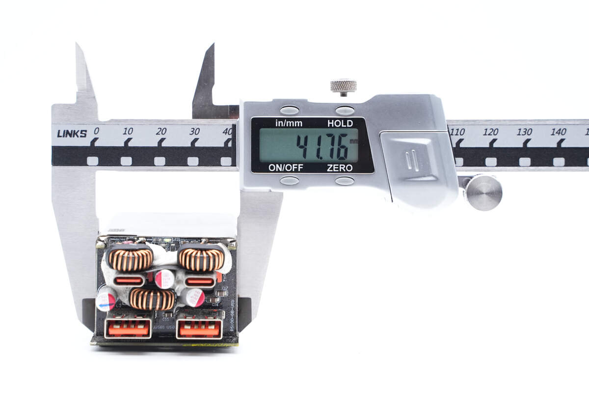
The width is about 42mm (1.65 inches).
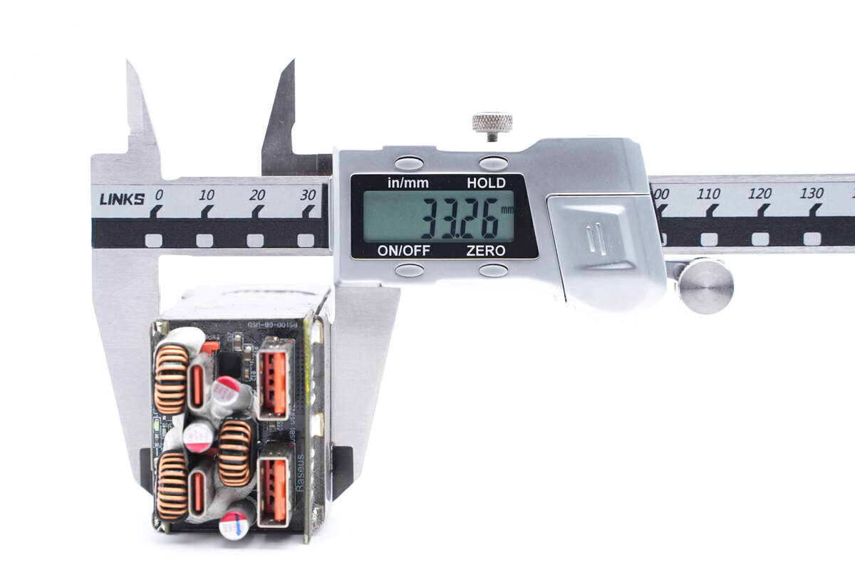
And the height is about 33mm (1.02 inches).
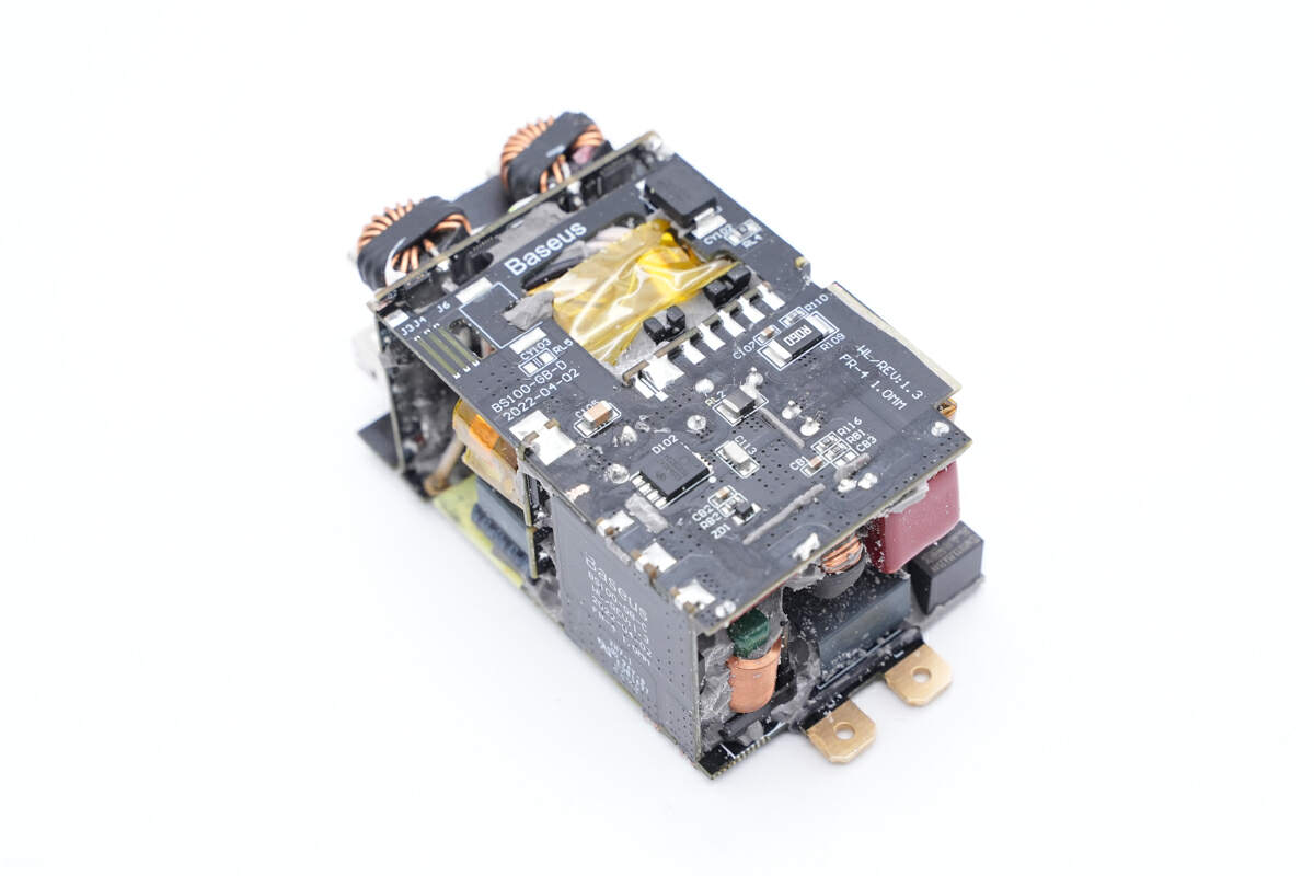
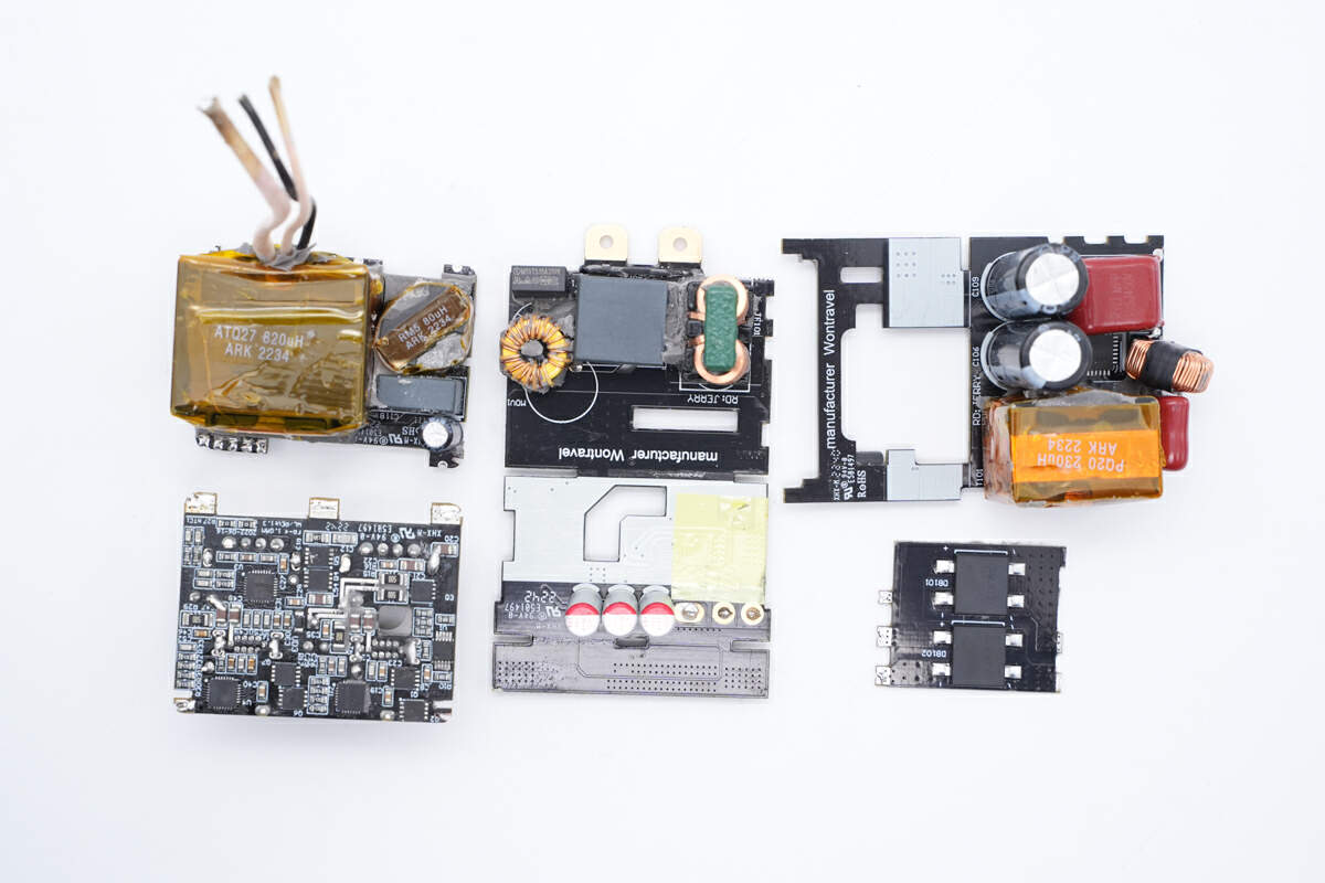
It consists of multiple PCBs to make full use of the space.
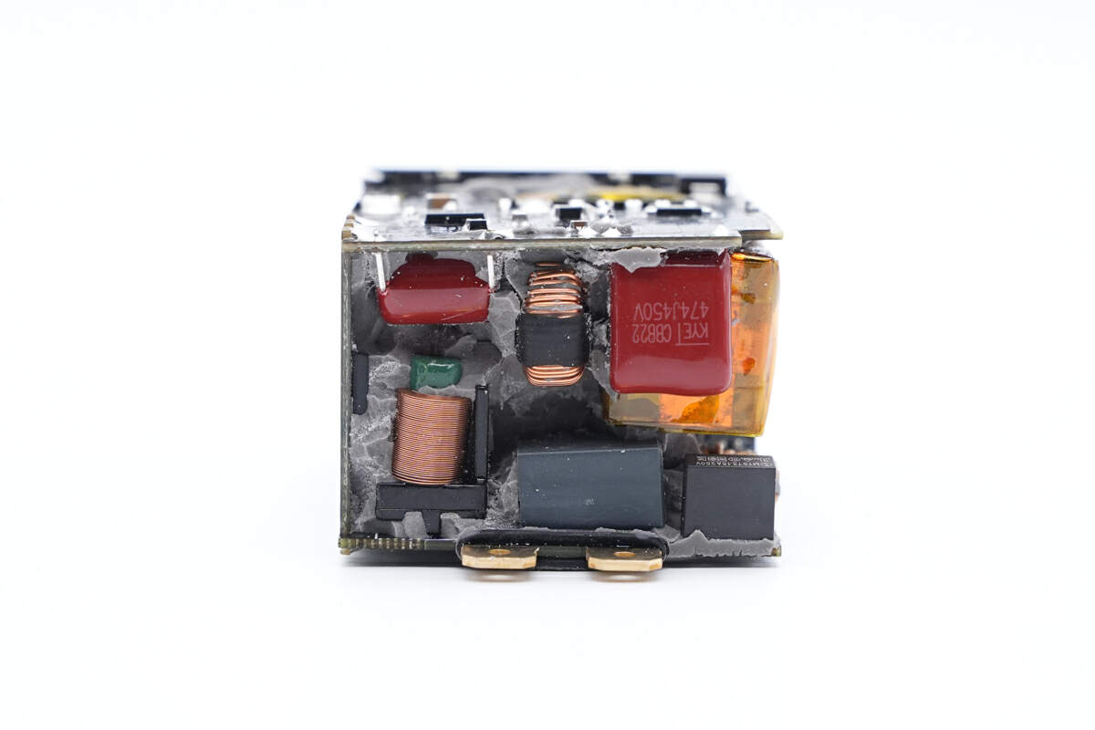
The fuse, common mode choke, and film capacitor are on the input end.
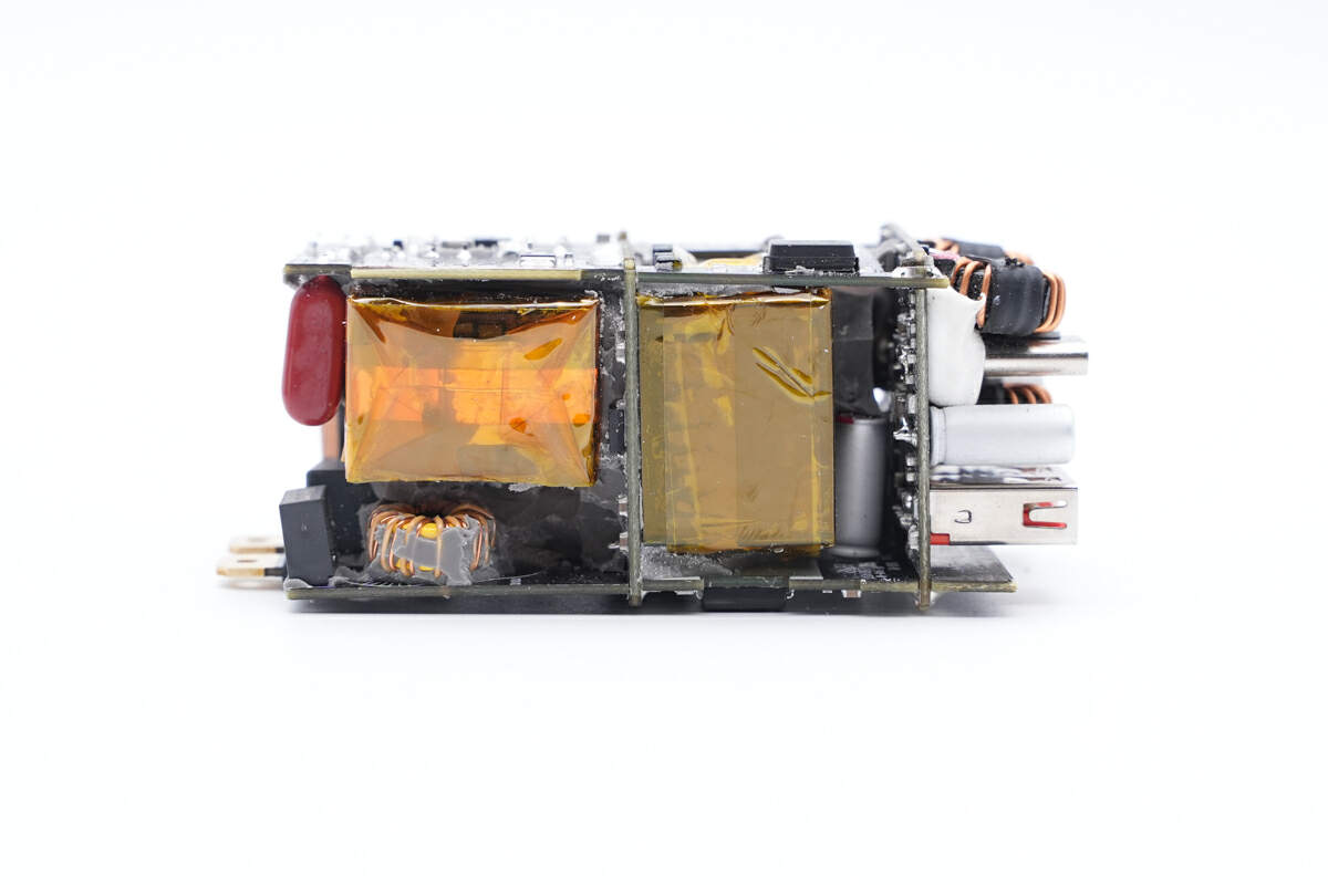
And the PFC boost inductor, LLC transformer, and fast charge synchronous buck circuit are on here.
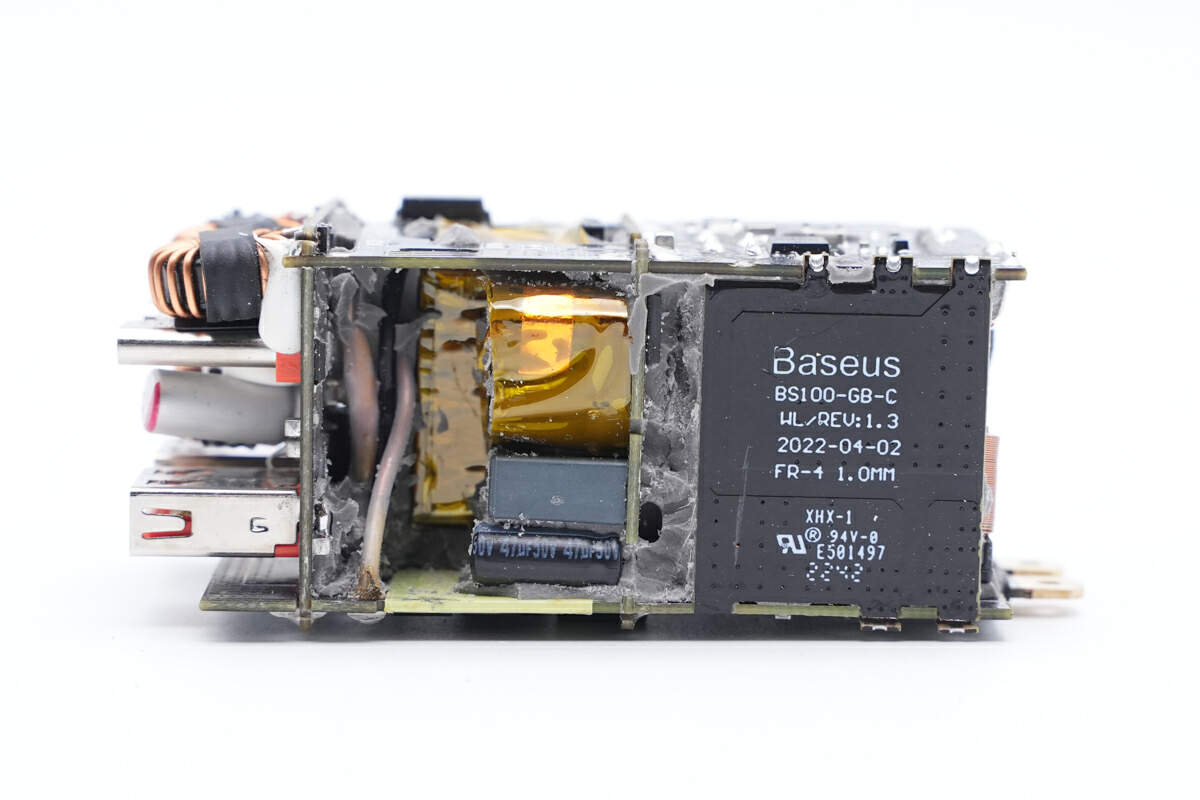
Here are the bridge rectifier, LLC transformer and related circuits.
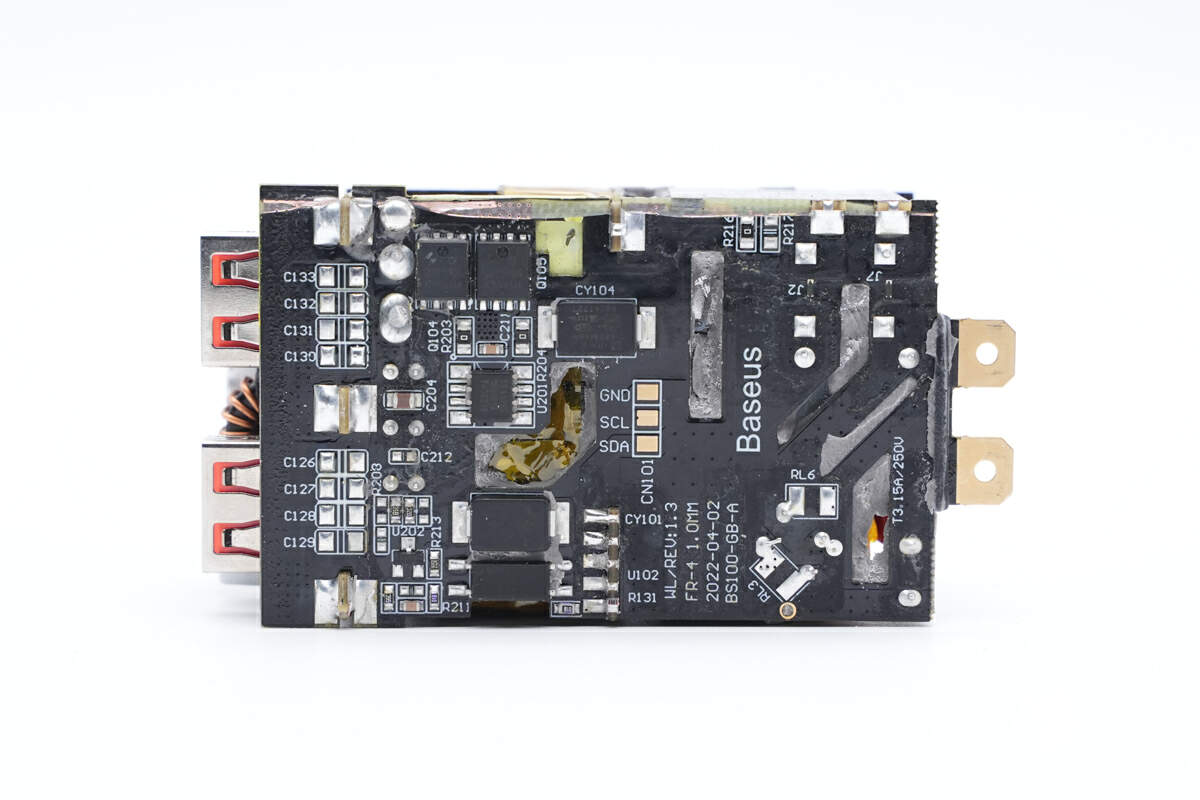
The SMD Y capacitor, feedback optocoupler, and synchronous rectification circuit are on this side.
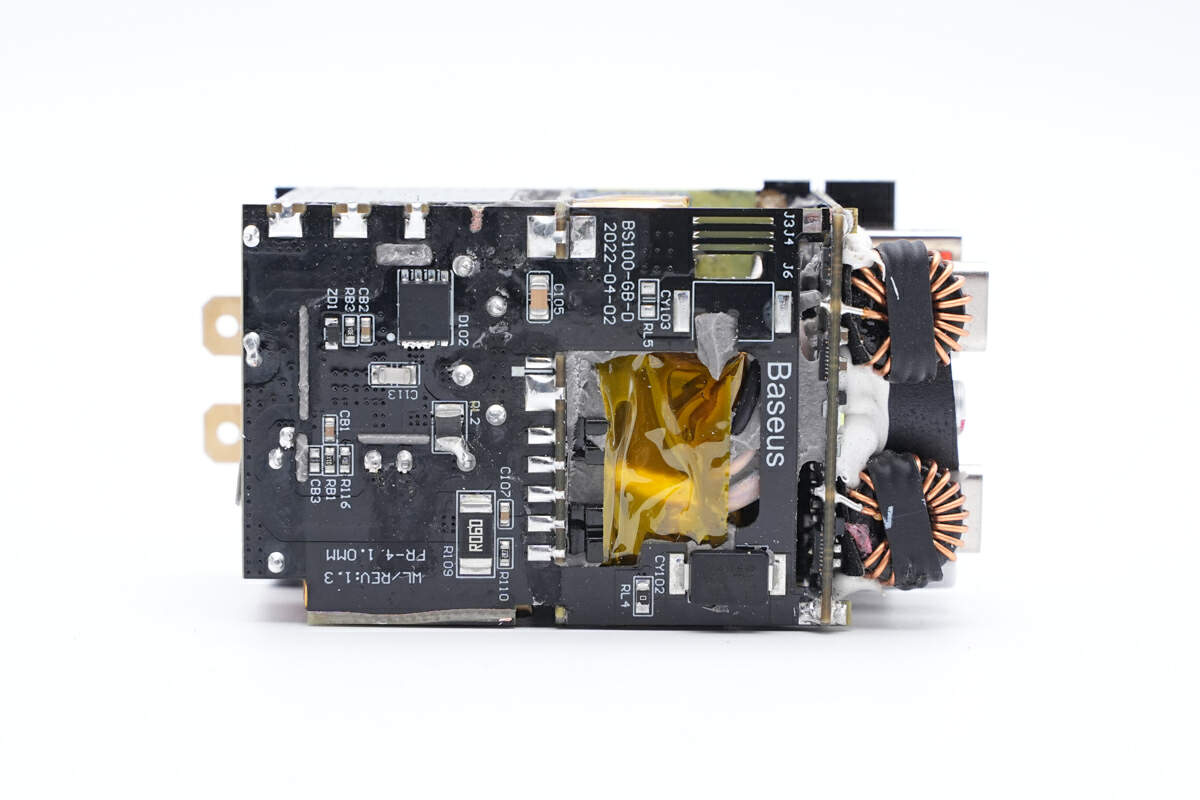
And the diode and current sampling resistor, as well as SMD Y capacitor are on the other side.
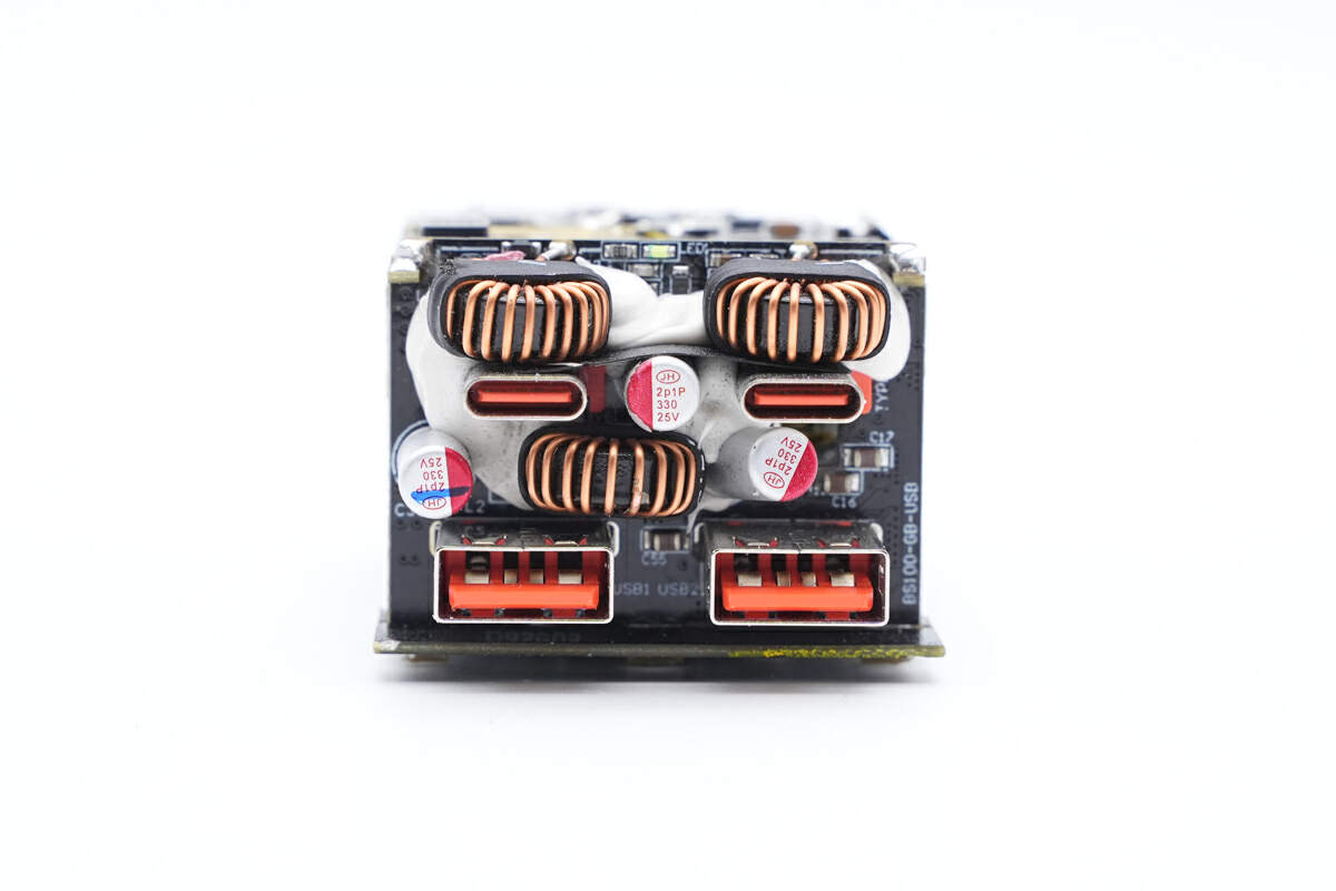
This are the three buck inductors and filter capacitors, corresponding to the USB module.
ChargerLAB found it adopts LLC topology and has a PFC circuit.
The current will be filtered by synchronous rectification circuit for output. Next, let's introduce every single component.
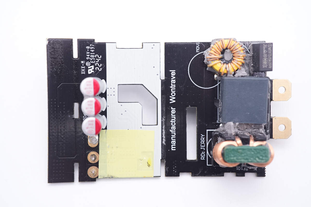
The fuse, NTC thermistor, safety X2 capacitor, and common mode choke solid capacitor are on here.
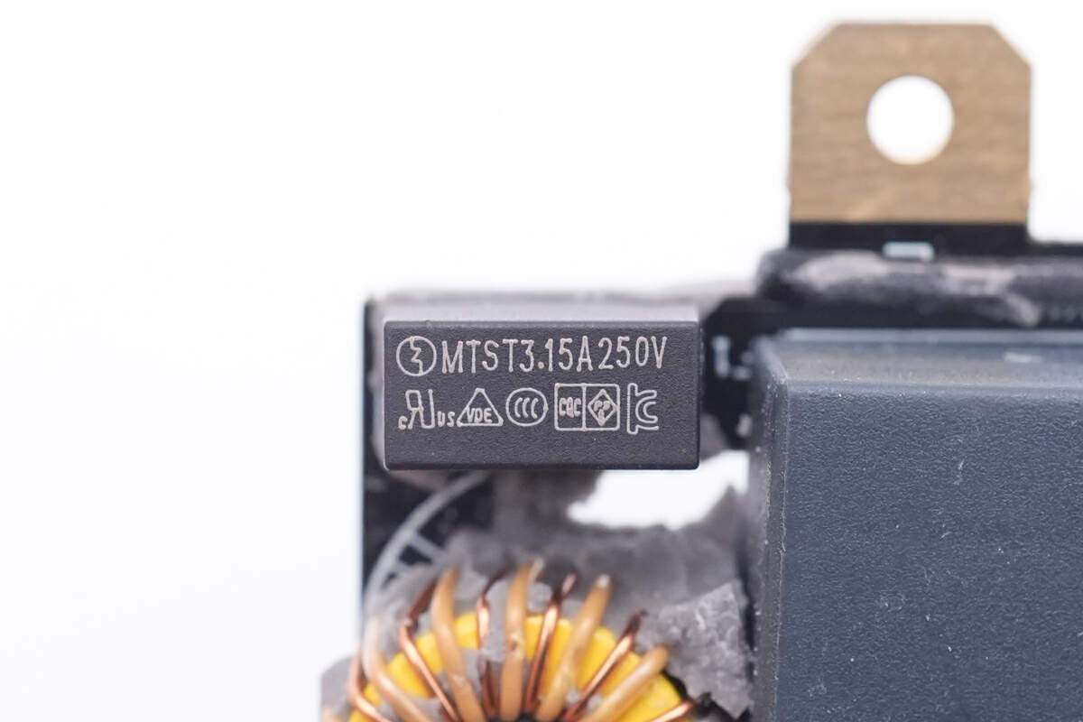
The input time-delay fuse is 3.15A 250V.
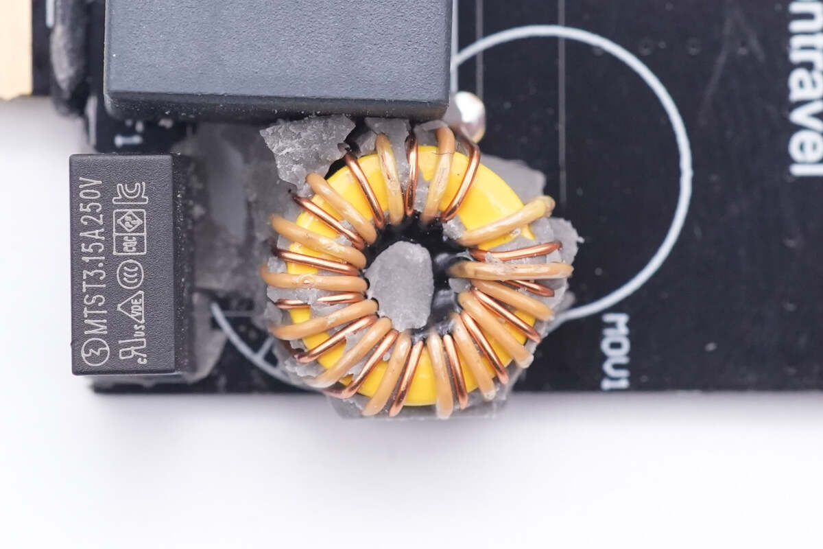
The first orange common mode choke is wound with insulated wires and magnet wires.
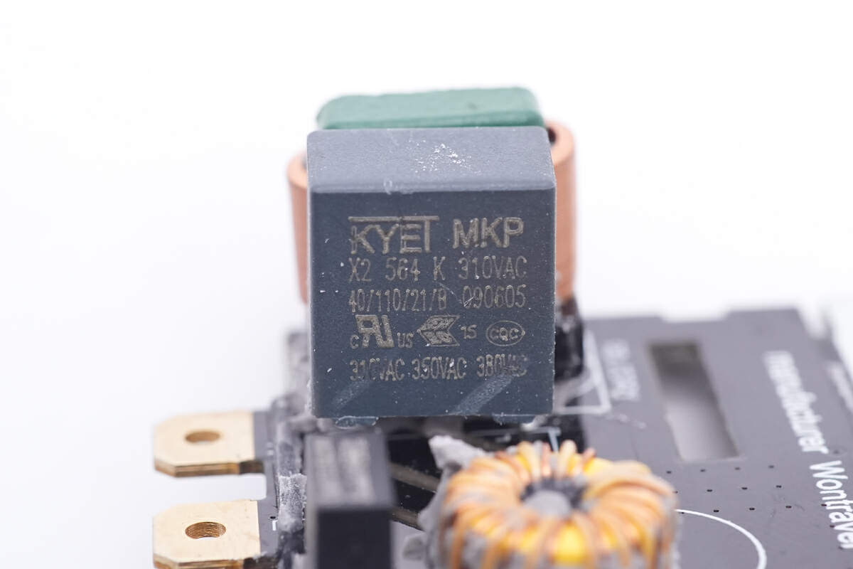
The safety X capacitor is from KYET Electronics, and the capacity is 0.56μF.
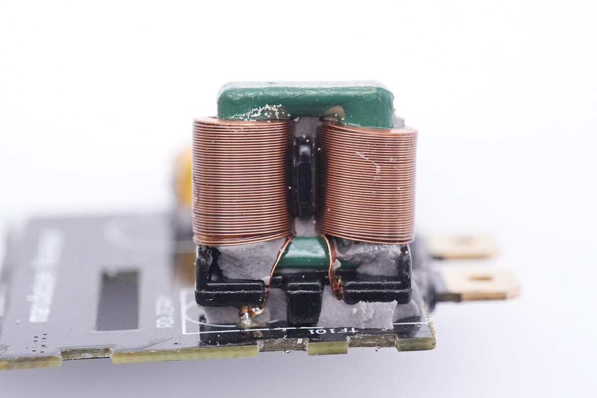
And the second green common mode choke is wound with flat copper wires.
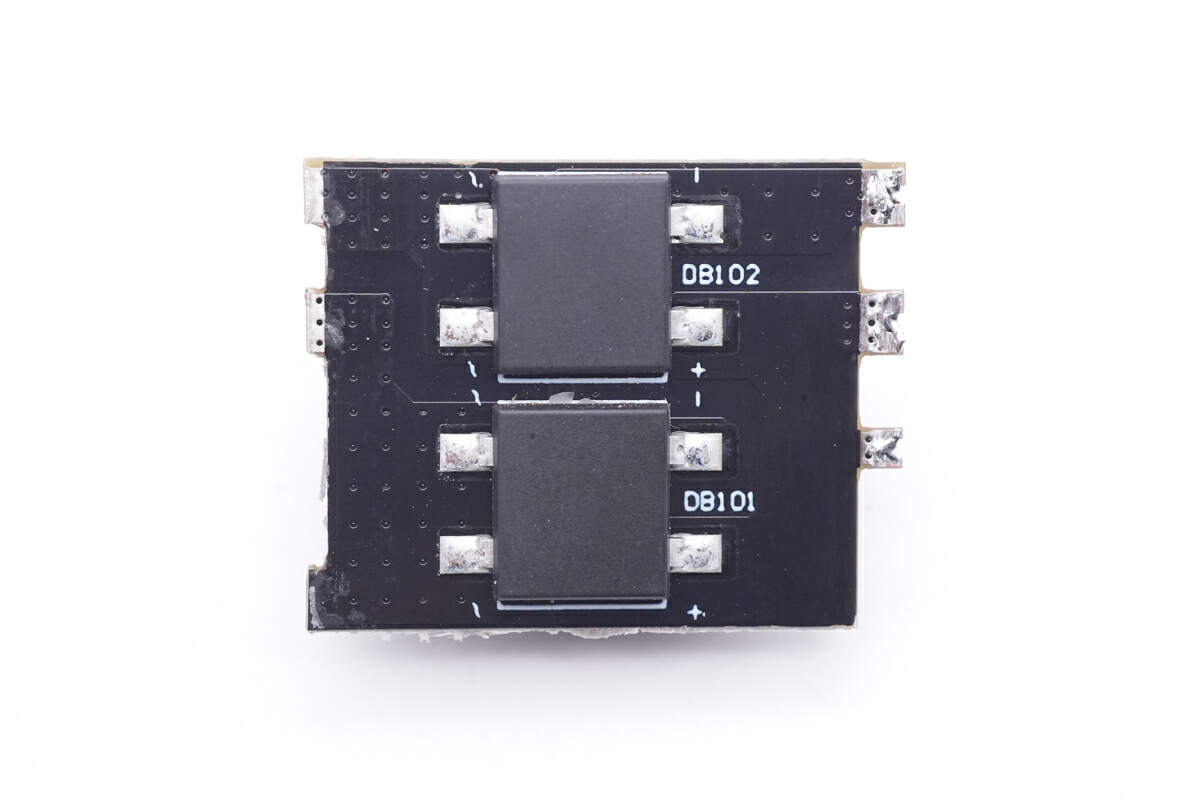
After EMI circuit filtering, the AC is sent to the bridge rectifier, and it rectifies the AC into pulsating DC for the PFC circuit.
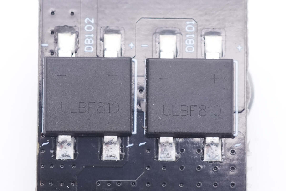
Two bridge rectifiers are connected in parallel to dissipate heat evenly. Model is ULBF810.
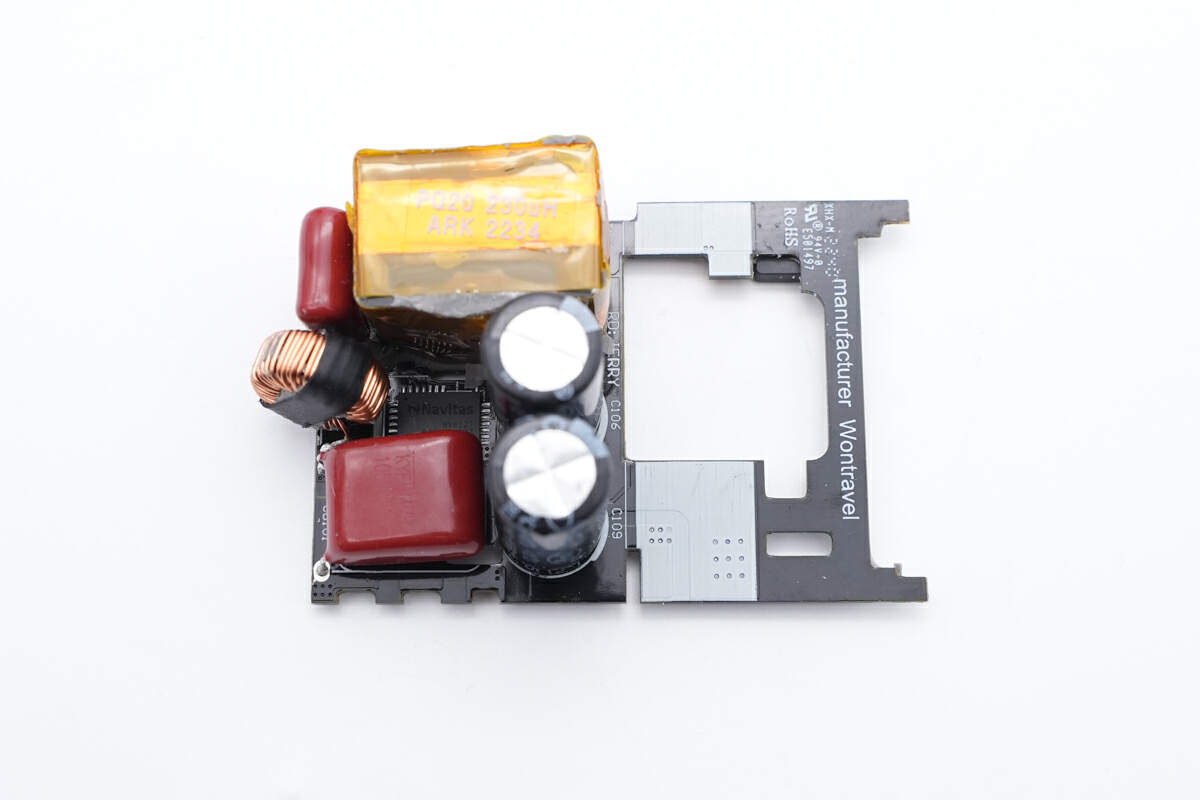
The pulsating DC after rectification is sent to the PFC small PCB, and the PFC circuit boosts and performs power factor correction. The front of the small PCB is soldered with GaN power chips, boost inductors, and filter capacitors, etc.
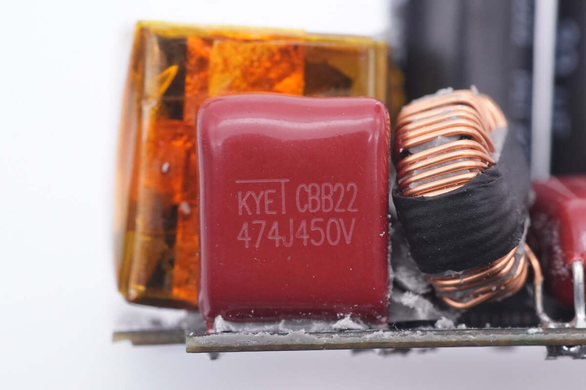
The red film capacitor is from the Kyet CBB22 series. 0.47μF 450V.
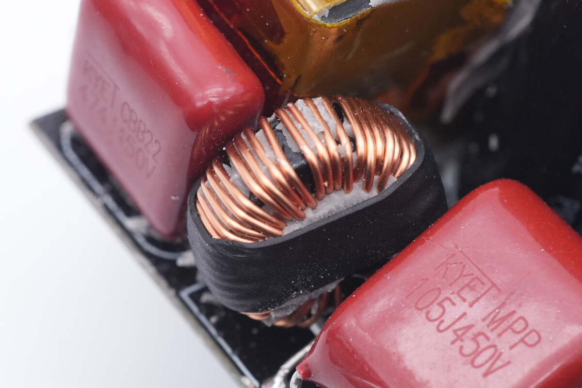
The toroidal core inductor is wrapped with heat-shrinkable tubing.
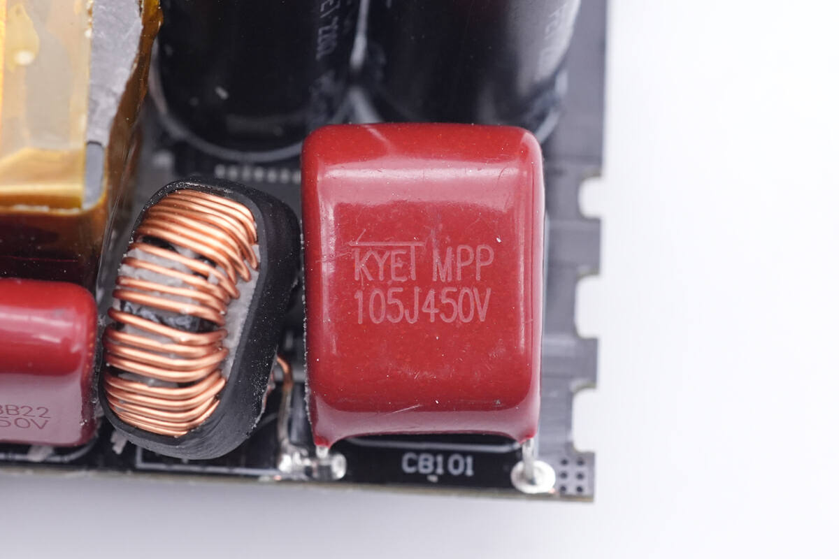
And this red film capacitor is also from the Kyet CBB22 series. 1μF 450V.
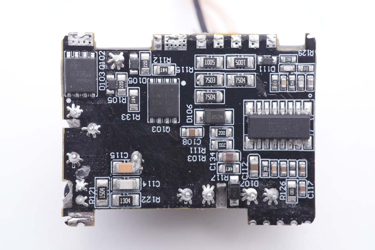
The master control chip is soldered on the interlayer PCB.
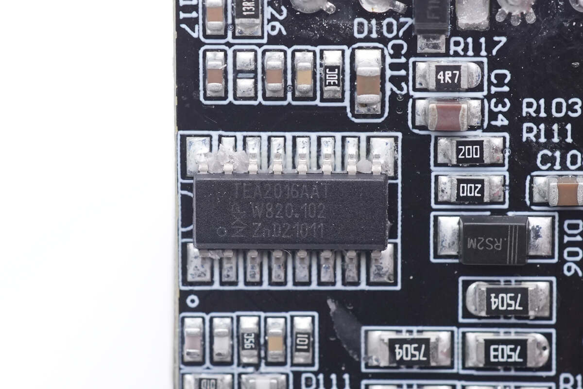
The primary PWM master control chip uses NXP's TEA2016AAT, which integrates an LLC controller and a PFC controller, and has a digital architecture to simplify design while reducing the number of peripheral components. The chip has multiple protection functions and high integration.
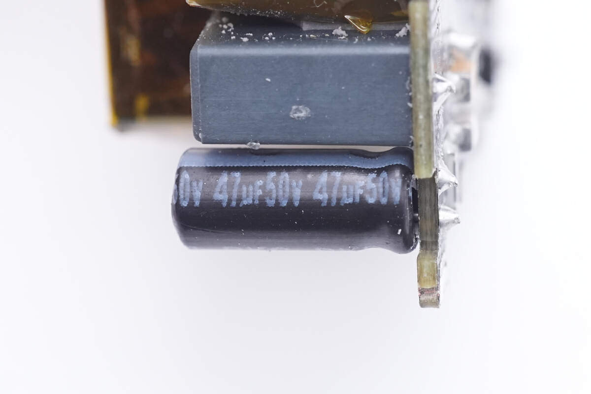
This tiny capacitor can power the master control chip, from Yongming. 47μF 50V.
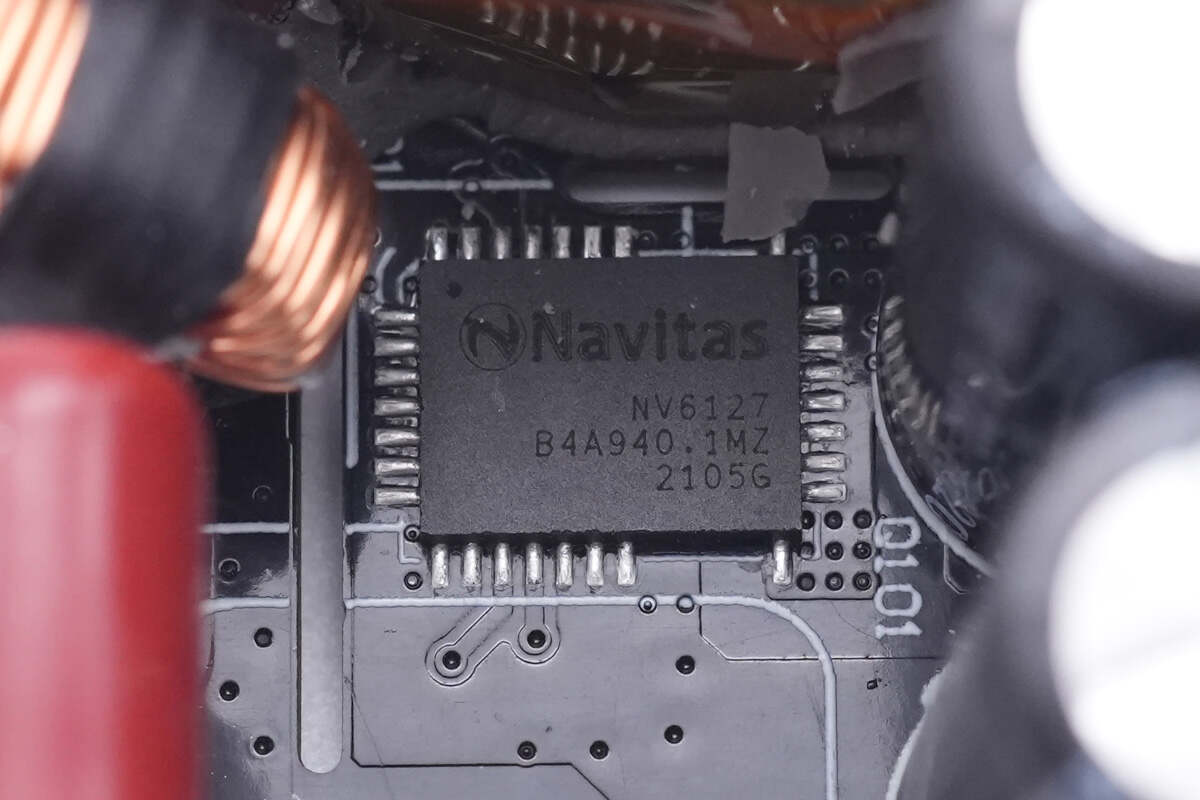
The NV6127 GaN IC for PFC boost is from Navitas, which integrates GaN FET, GaN driver, and logic circuit. The NV6127 adopts QFN6 x 8 package, upgraded heat dissipation performance, 125mΩ conduction resistance, and built-in driver support for 10-30V power supply. It supports a maximum switch frequency of 2MHz.
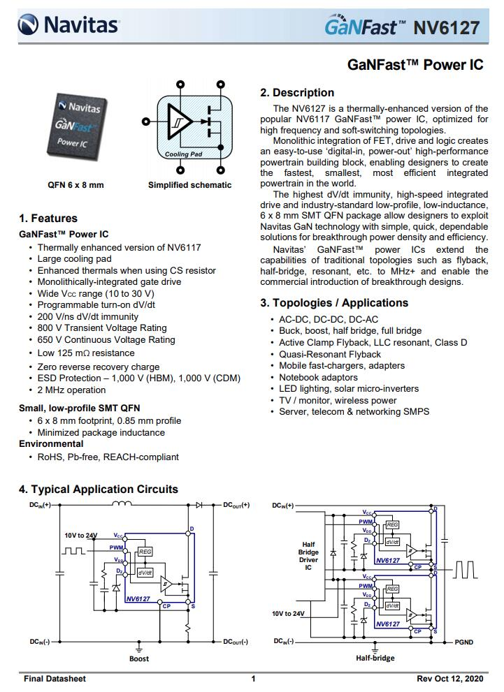
Here is all the information about NV6127.
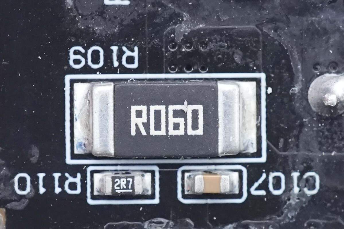
This sampling resistor is used to detect the current of the PFC circuit. Resistance is 60mΩ.
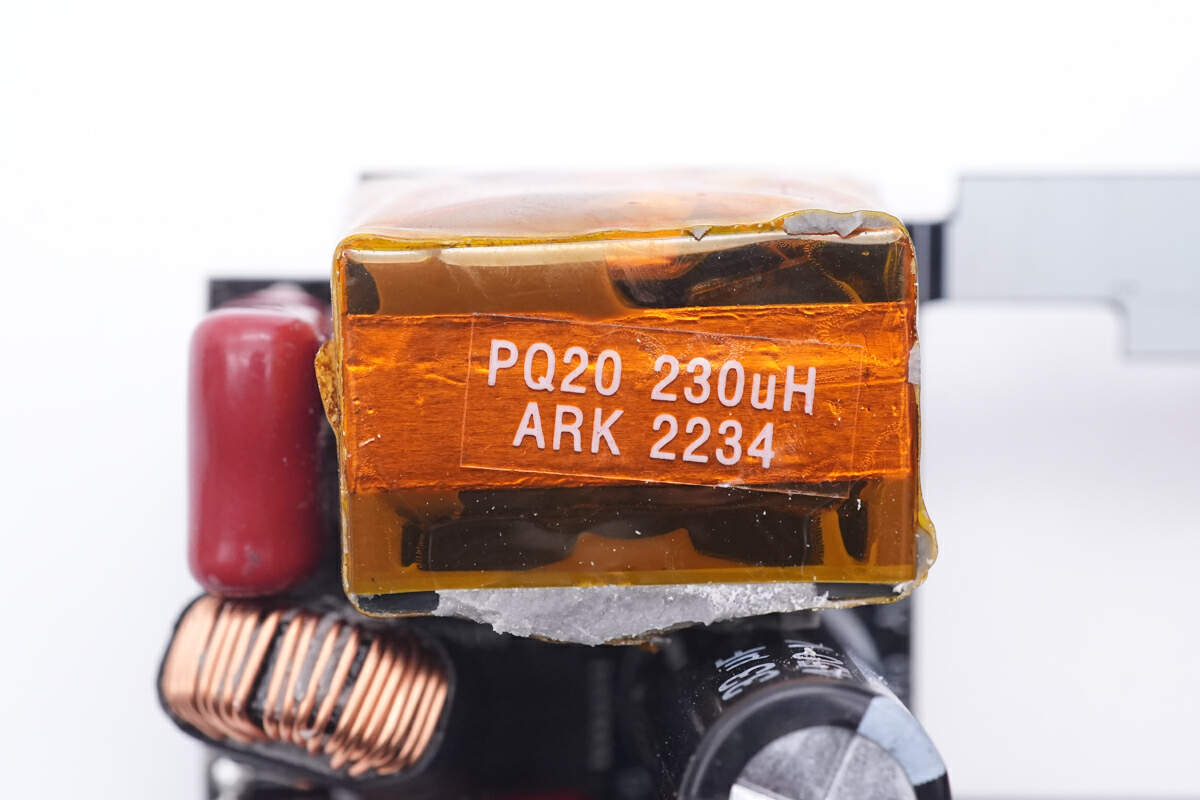
The PFC boost inductor is tightly wound and insulated with heat-resistant tape, and the ferrite core is PQ20.
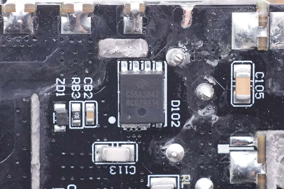
The PFC rectifier is from Global Power and adopts DFN5 x 6 package. It's a silicon carbide diode with 650V withstand voltage and 4A current. Model is G5S6504Z.
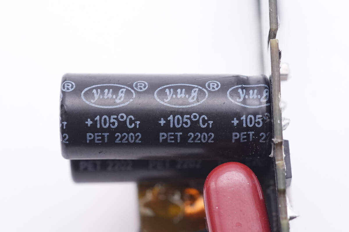
Two electrolytic capacitors for high-voltage filtering are from Yuguang Electronics.
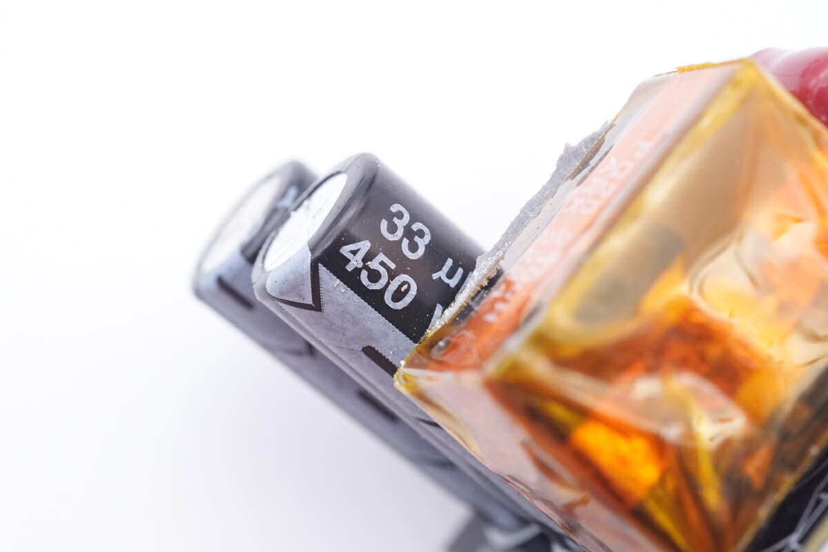
And thoes two electrolytic capacitors are connected in parallel for output filtering of PFC boost circuit. 33μF 450V for each.
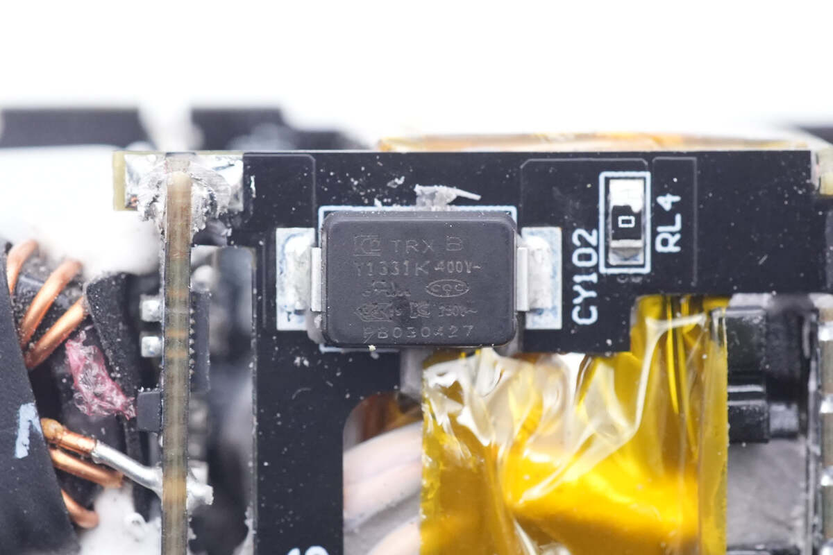
The SMD Y capacitor is from TRX, which features in small size and light weight, and are very suitable for high-density power supply products such as GaN charger.
TRX focuses on the R&D, production and sales of passive components, with a registered capital of 100 million yuan. It has two types of capacitor brands: SMD TRX and DIP TY capacitors. TRX will devote itself to the research of ceramic materials in order to provide customers with more solutions.
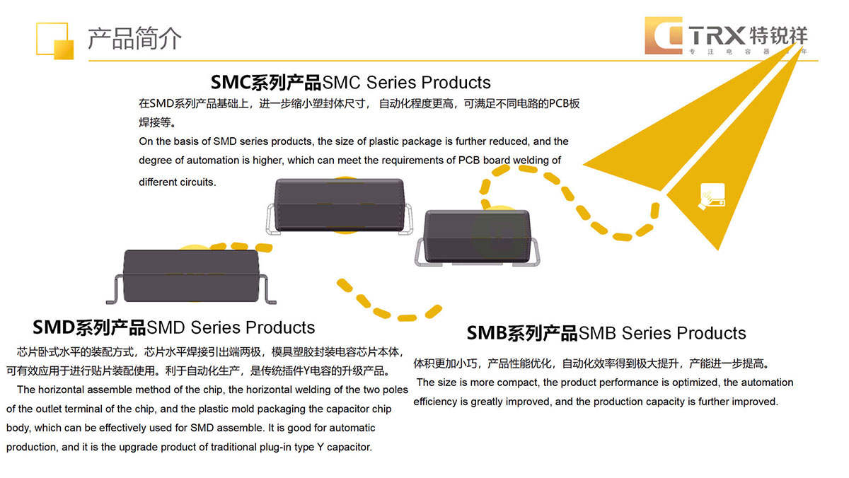
This is the introduction for TRX's products.
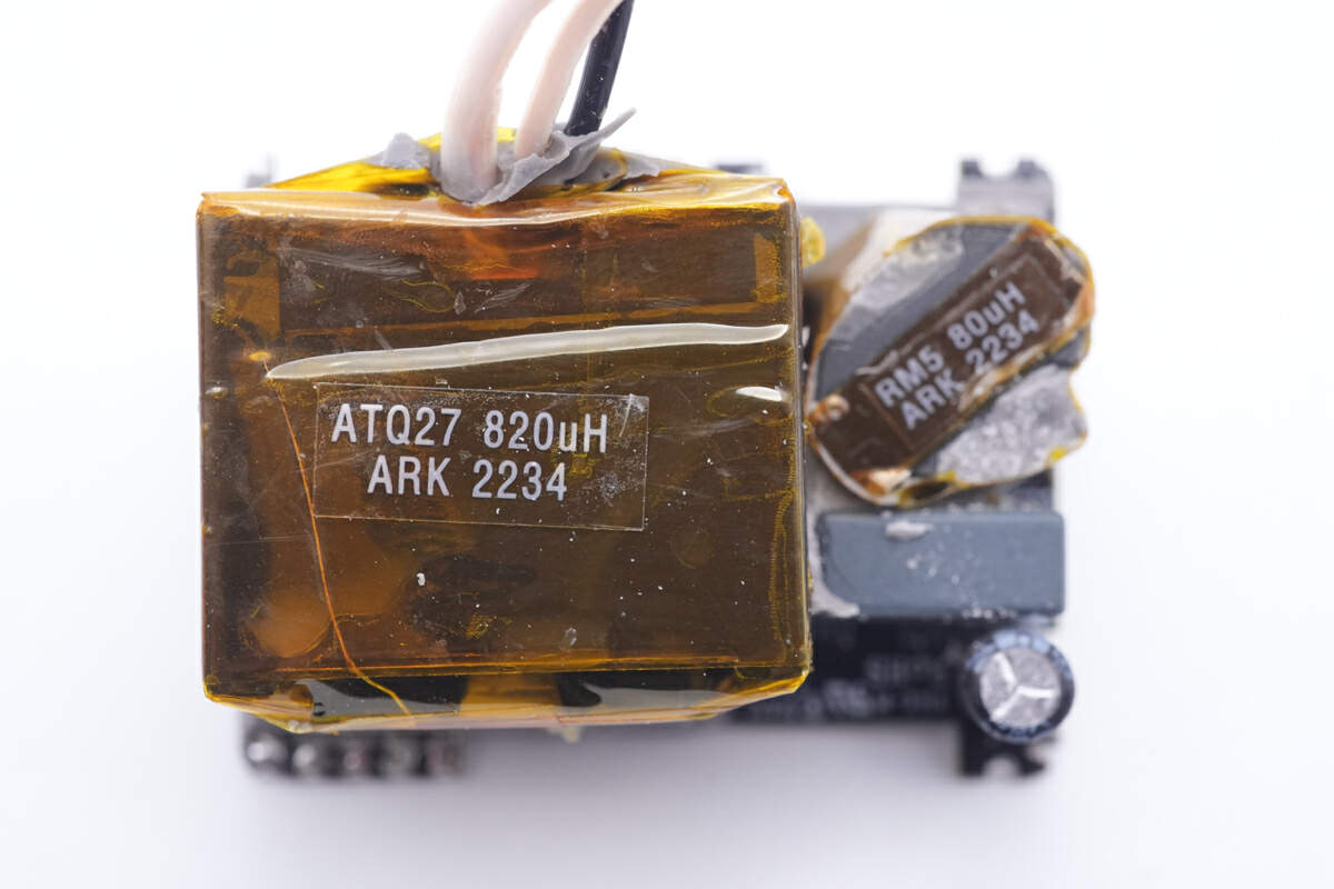
The LLC transformer, resonant capacitor and resonant inductor are on the internal PCB, as well as the filter capacitor for the power supply of the master control chip.
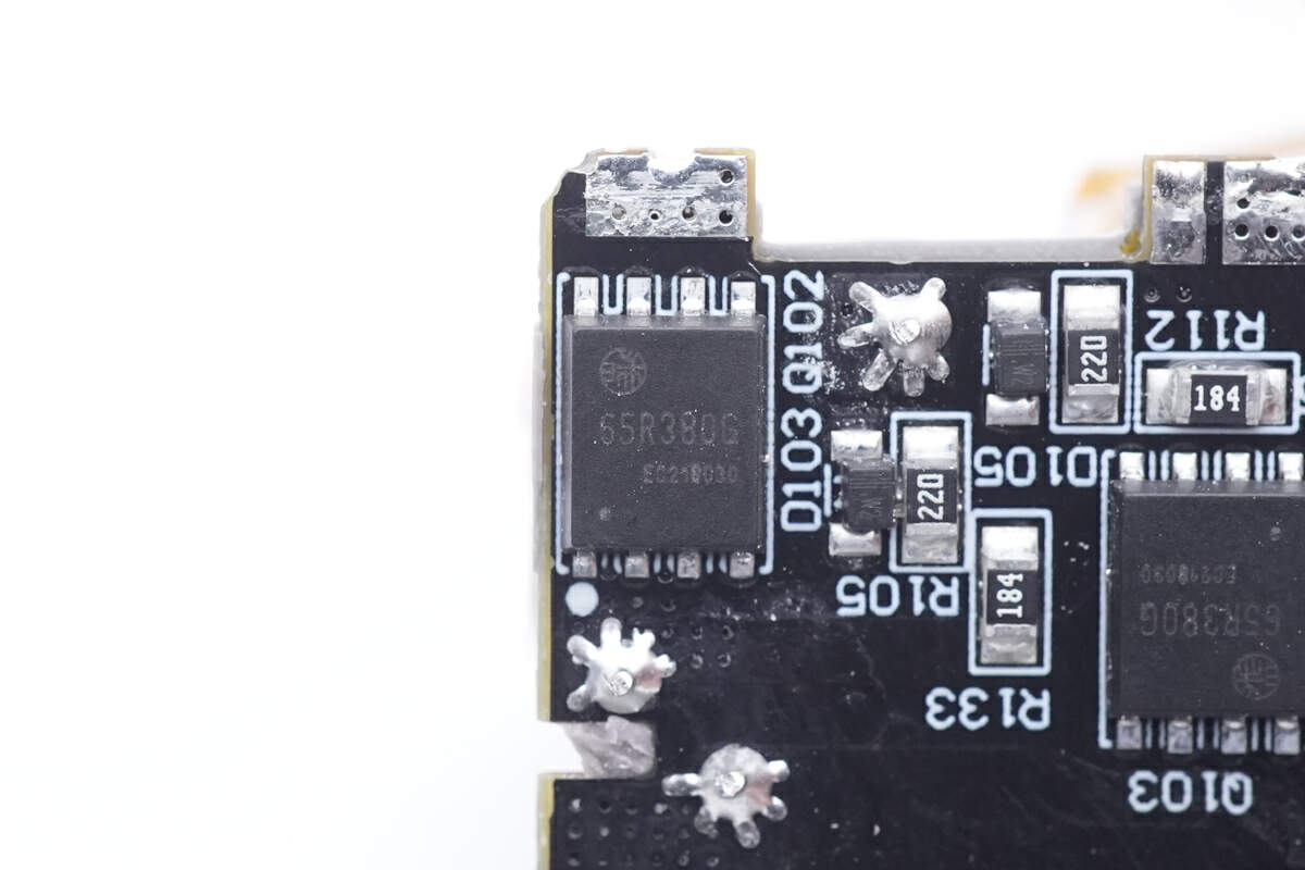
The LLC MOSFET is from HRmicro and adopts DFN5 x 6 package. Model is HRM65R380G. 650V 340mΩ.
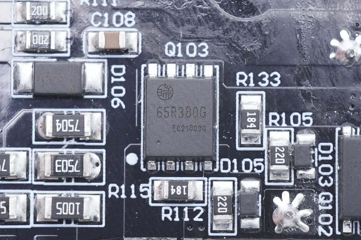
And this is another same MOSFET, which can form an LLC half bridge.
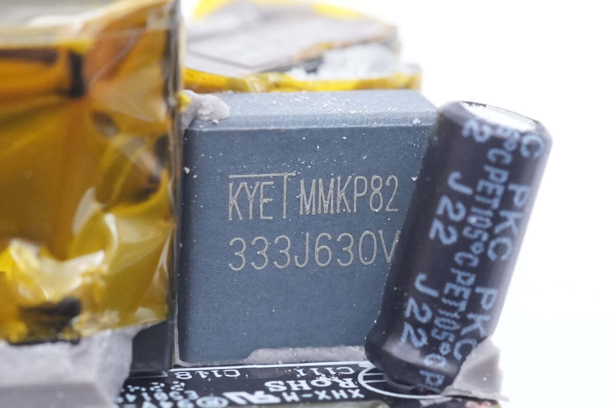
The resonant capacitor is from Kyet. 0.033μF 630V.
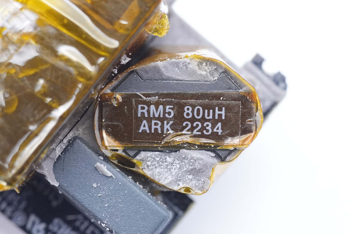
The resonant inductor has an inductance of 80μH, and the ferrite core is RM5.
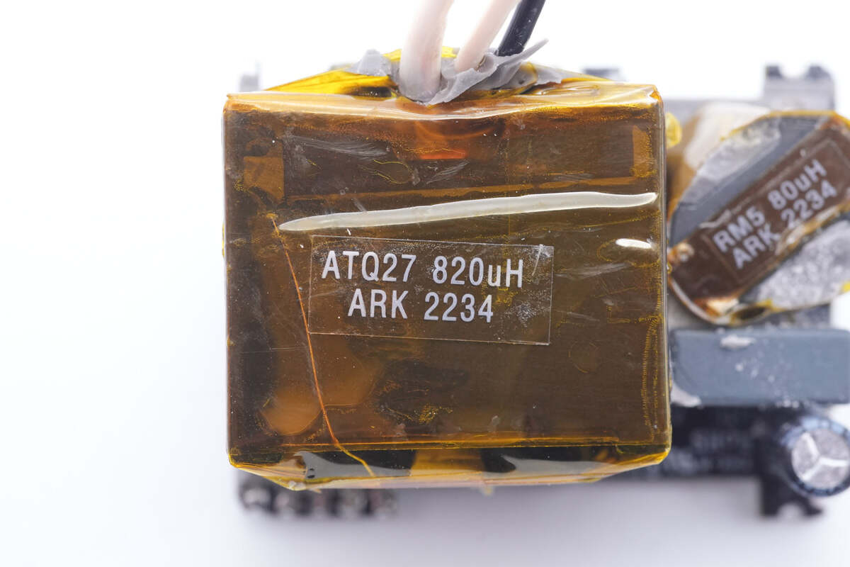
The transformer is tightly wound and insulated with heat-resistant tape, and the ferrite core is ATQ27.
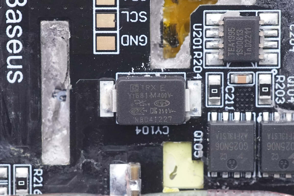
This SMD Y capacitor marked with TMY1681M is from TRX.
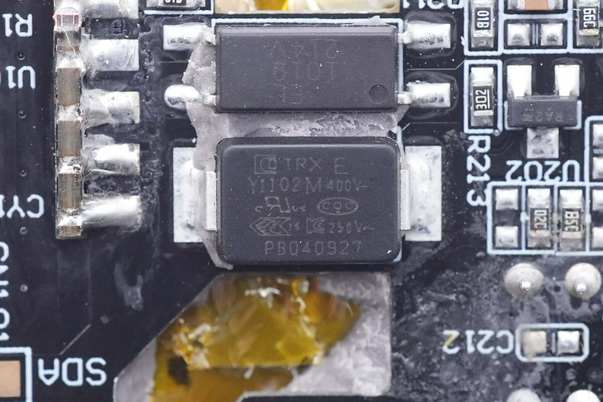
And this SMD Y capacitor marked with TMY1102M is also from TRX.
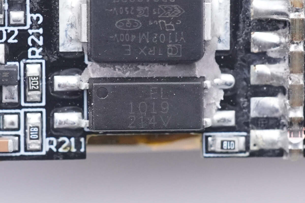
And the EL1019 optocoupler is used to regulate output power.
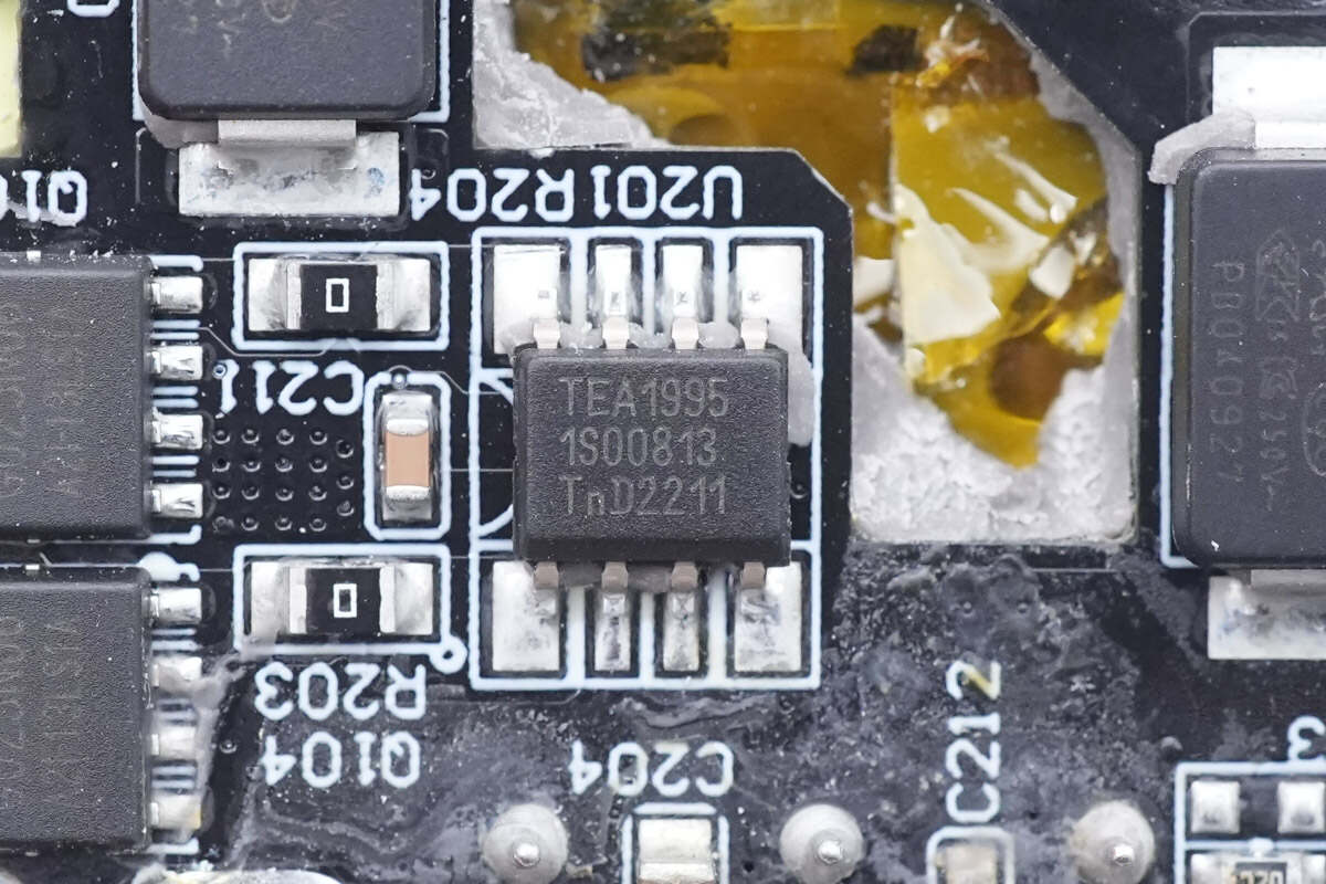
The synchronous rectifier controller is from NXP, model TEA1995, which contains two independent drivers for LLC. The peripheral components are streamlined, supporting a working voltage of 38V, and can meet the 28V output of USB PD3.1.
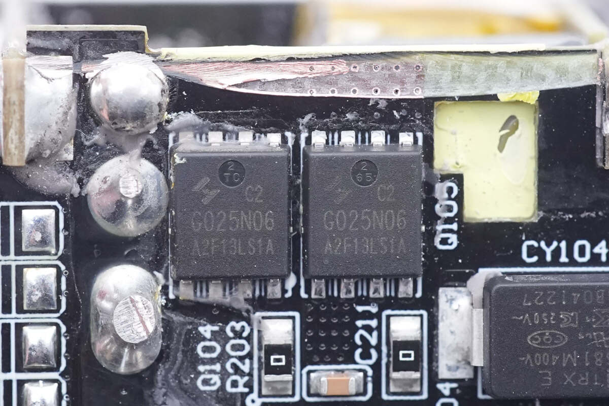
Those two synchronous rectifiers are from Huayi Micro and adopt PDFN8L package. 60V, 2.3mΩ. Model is HYG025N06LS2C2.
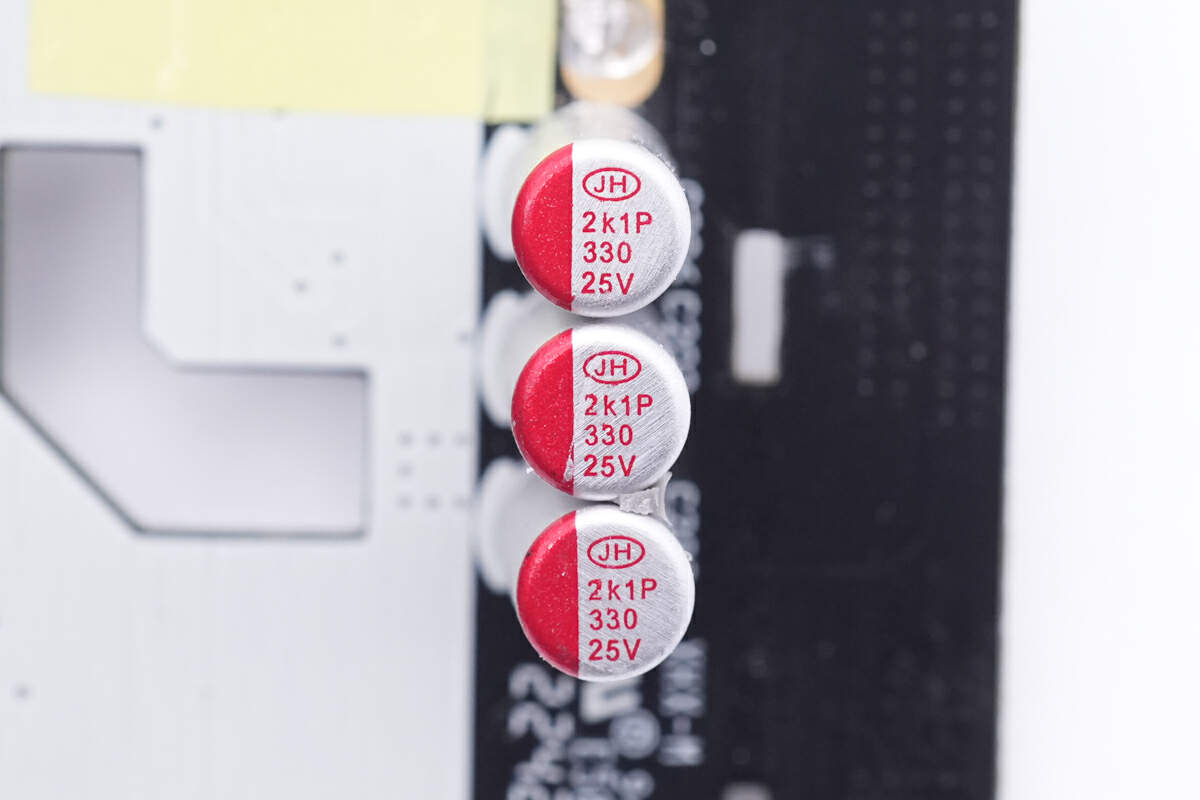
Those three solid capacitors for output filtering are connected in parallel, from Jianghai. 330μF 25V for each.
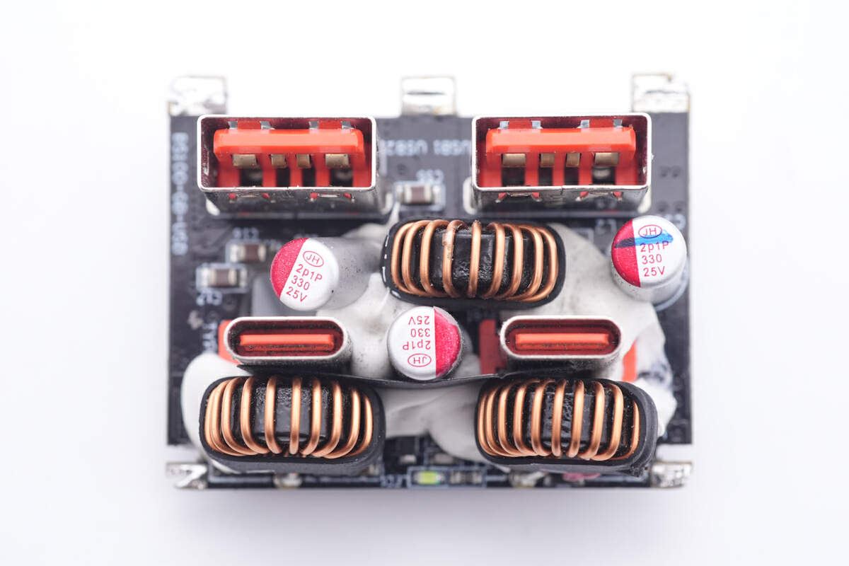
The USB-C connector and the toroidal core inductor are insulated with an isolation board and reinforced with adhesives.
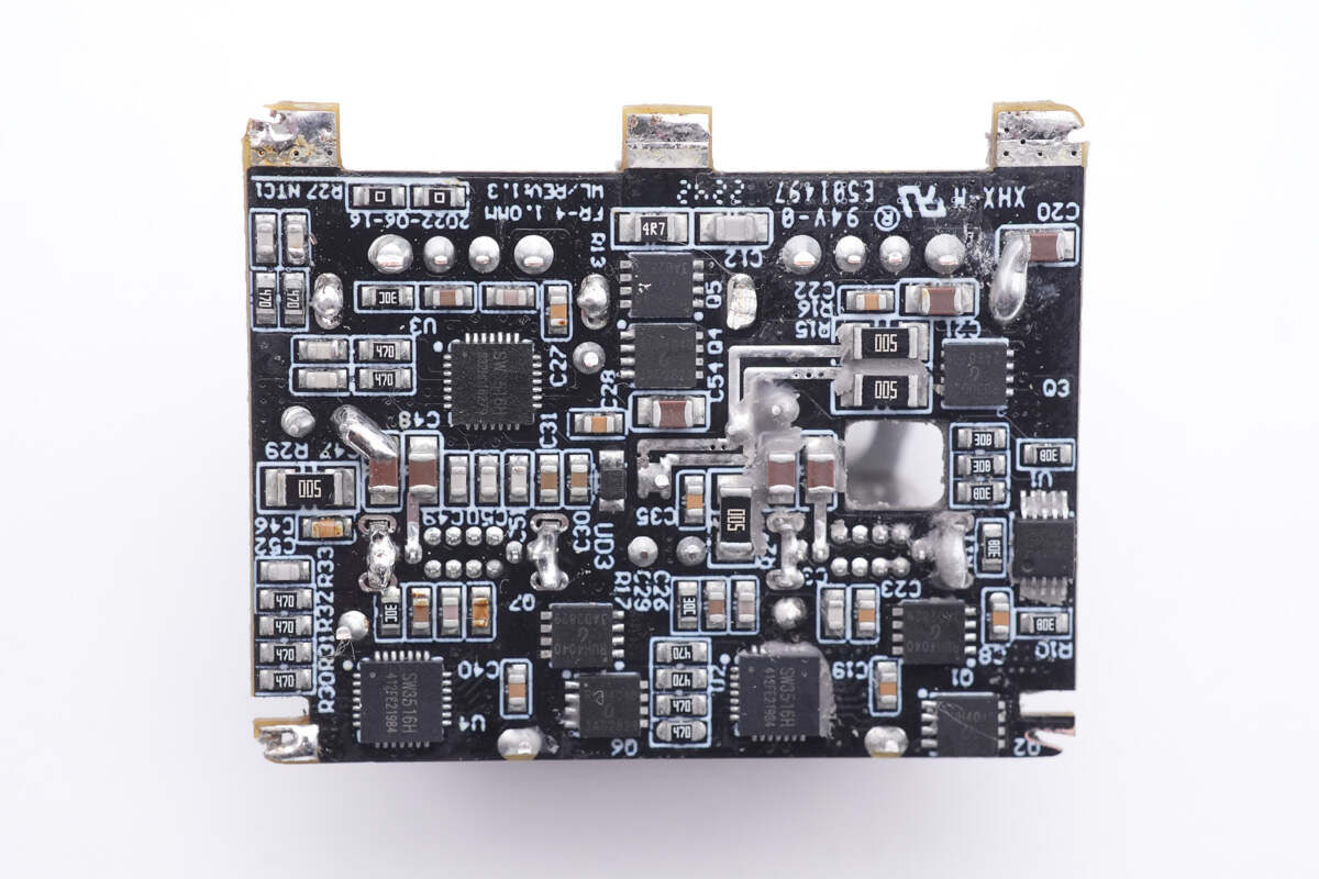
There're three independent buck circuits on the output PCB, so there're three controller ICs. Two USB-A ports share the same controller chip. And they're all from Ismartware with the same model.
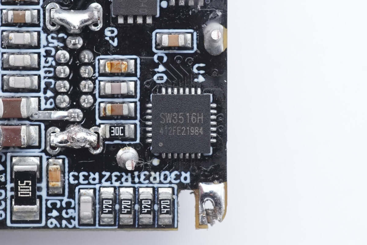
The model is SW3516H, it is used for buck control and protocol recognition. SW3516H is a highly integrated dual-port charging chip for multiple fast charging protocols, supporting fast charging output on USB-A plus USB-C port, independent current limiting on dual ports.
It integrated 5A high efficiency synchronous buck converter, and supports PPS, PD, QC, AFC, FCP, SCP, PE and SFCP fast charging protocols. The maximum output is 100W PD with CC/CV mode and dual-port management logic. Only a few peripheral devices are needed to form a complete high-performance dual-port charging solution for multiple fast charging protocols.
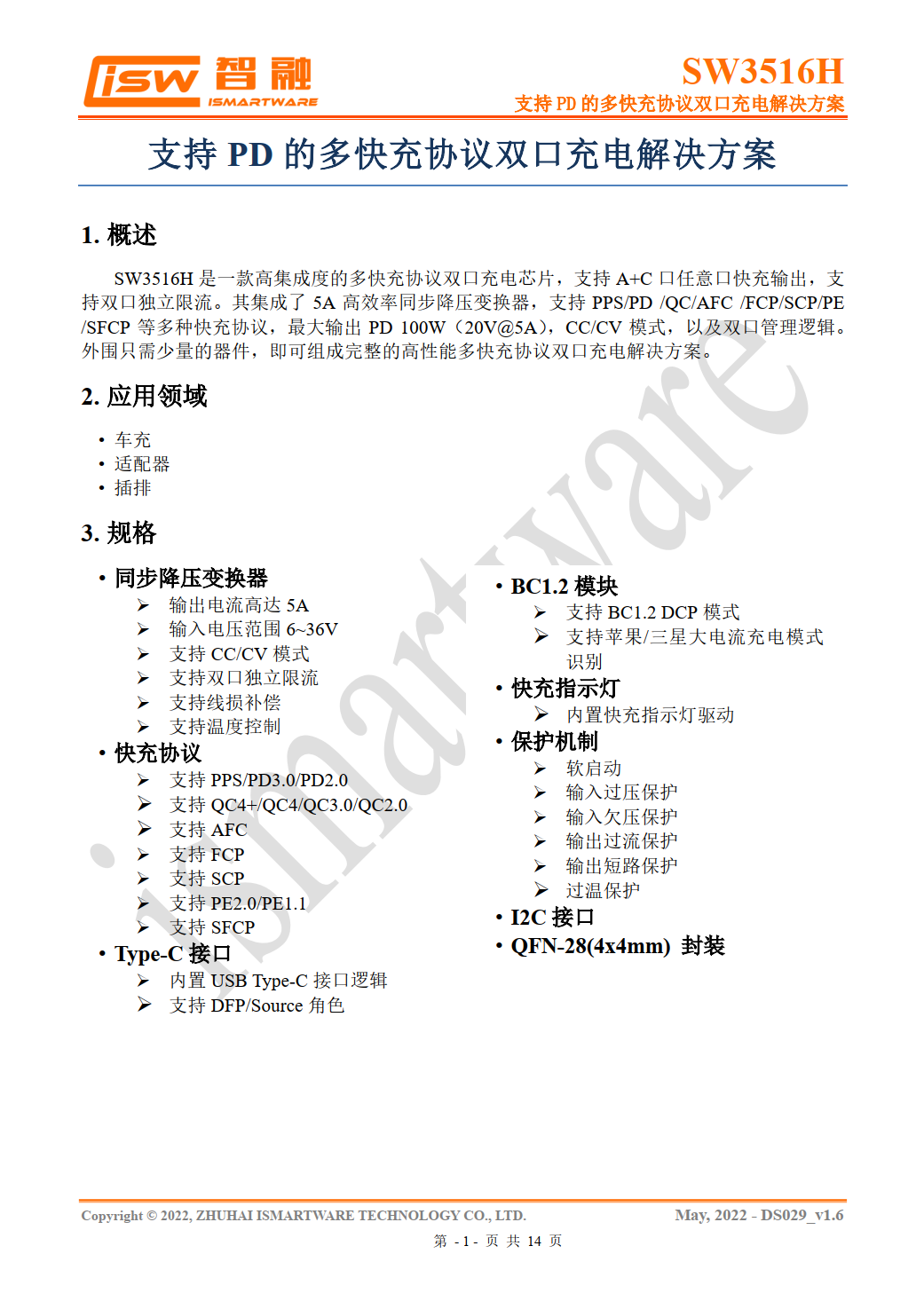
Here is all the information about SW3516H.
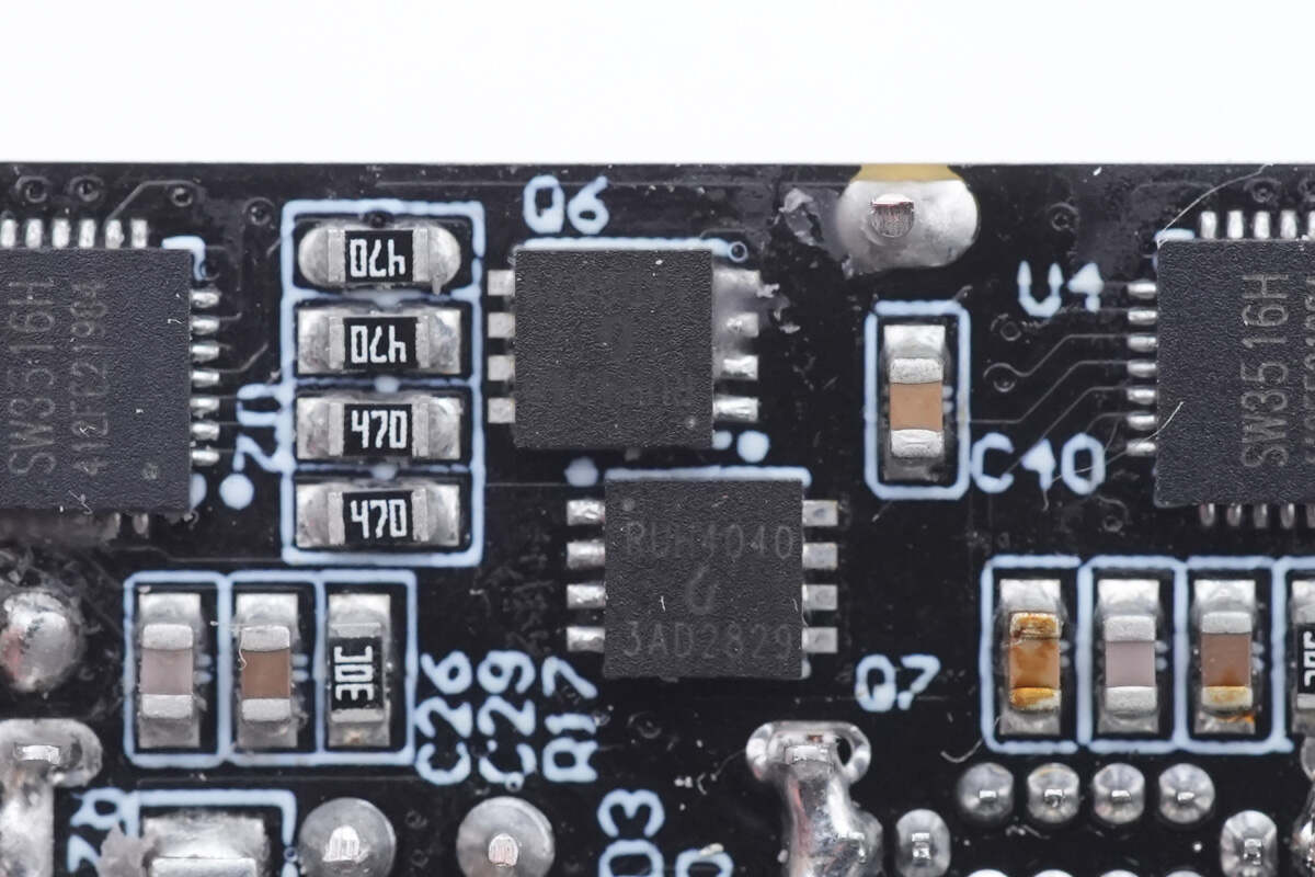
Each controller IC corresponds to two external MOSFETs for synchronous buck circuit. They are from Ruichips and adopt PDFN3333 package. 40V, 8mΩ. Model is RUH4040.
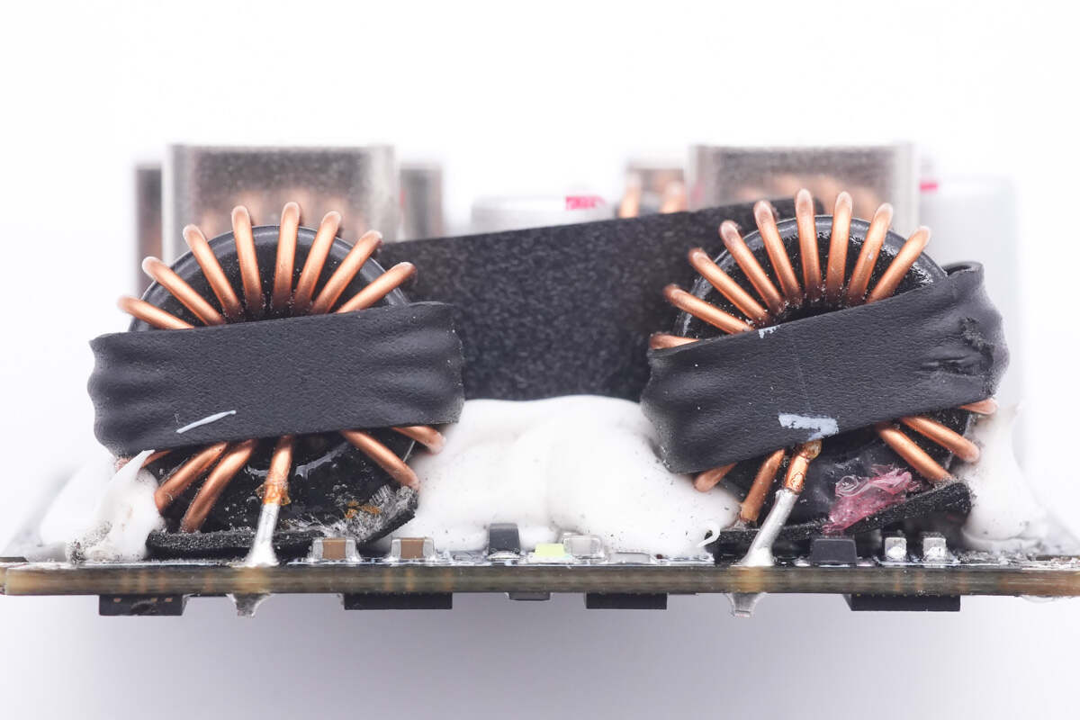
The two buck inductors are used for the USB-C.
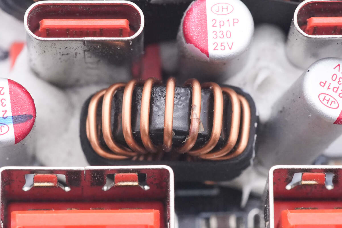
And this buck infuctor is used for USB-A.
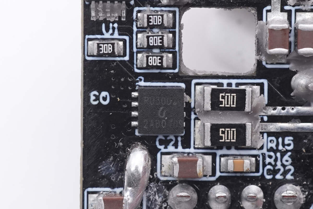
This VBUS MOSFET for two USB-A ports is from Ruichips and adopts PDFN3333 package. 30V 8.5mΩ. Model is RU30D20M2.
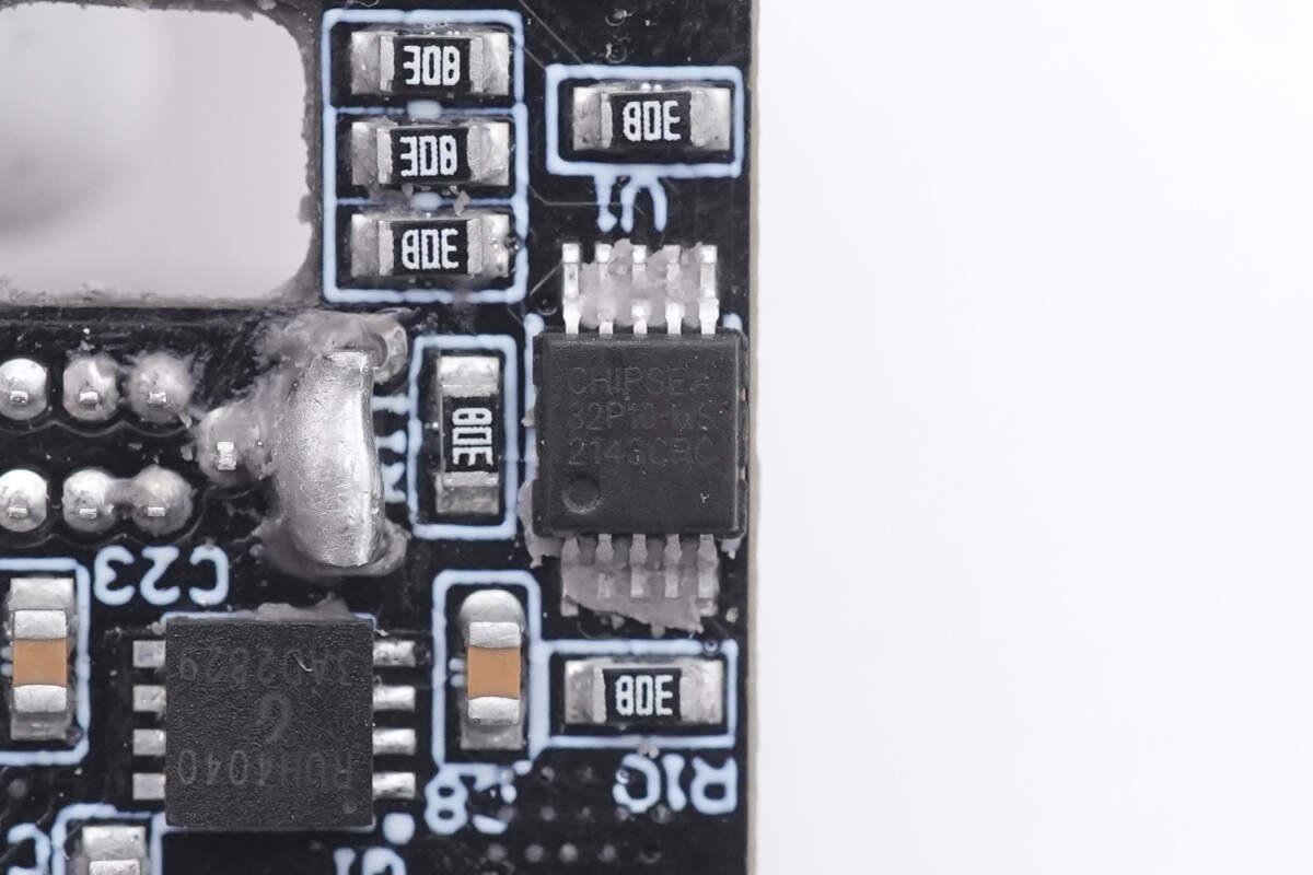
An 8-bit MCU from Chipsea integrates a 12-bit ADC and adopts MSOP10 package. It can automatically control the power distribution of four USB ports. Model is CSU32P10.
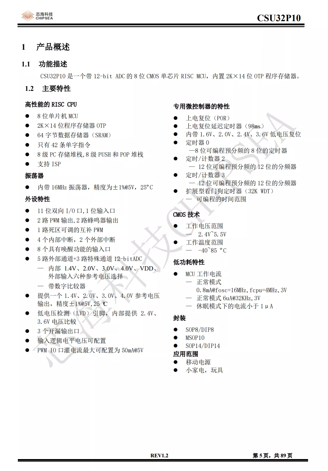
Here is all the information about CSU32P10.
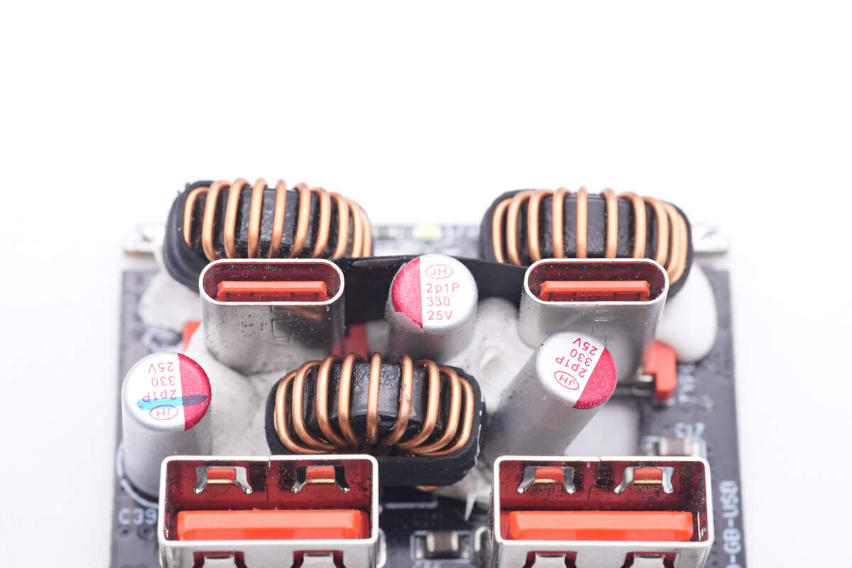
The plastic sheet inside the USB-C connector is red. Three Jianghai solid capacitors correspond to three buck outputs, all of which are 330μF 25V.
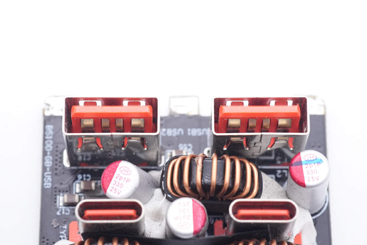
The USB-A connector is equipped with a red plastic sheet and its positive and negative poles are deliberately designed to be wider than traditional one for high current.
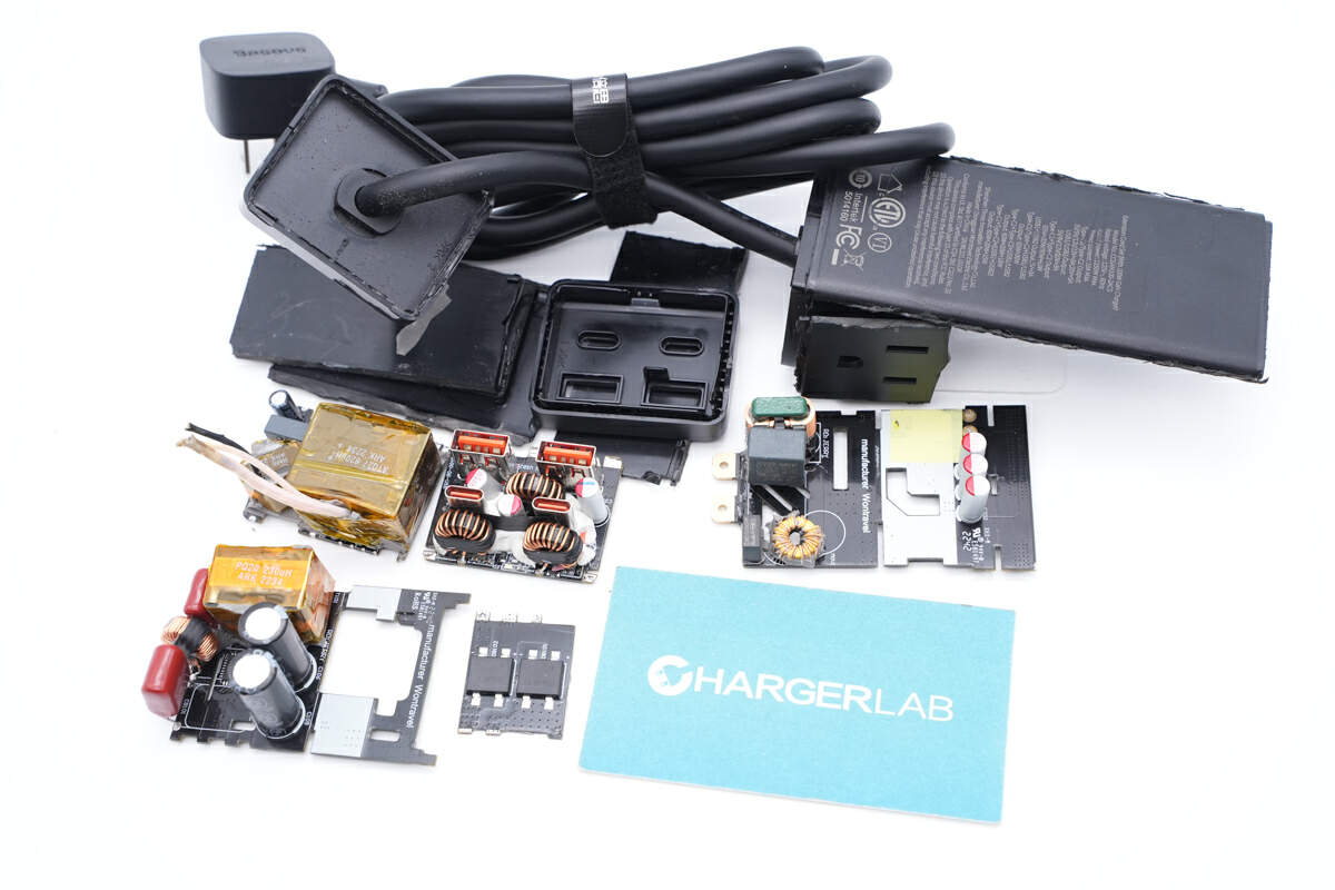
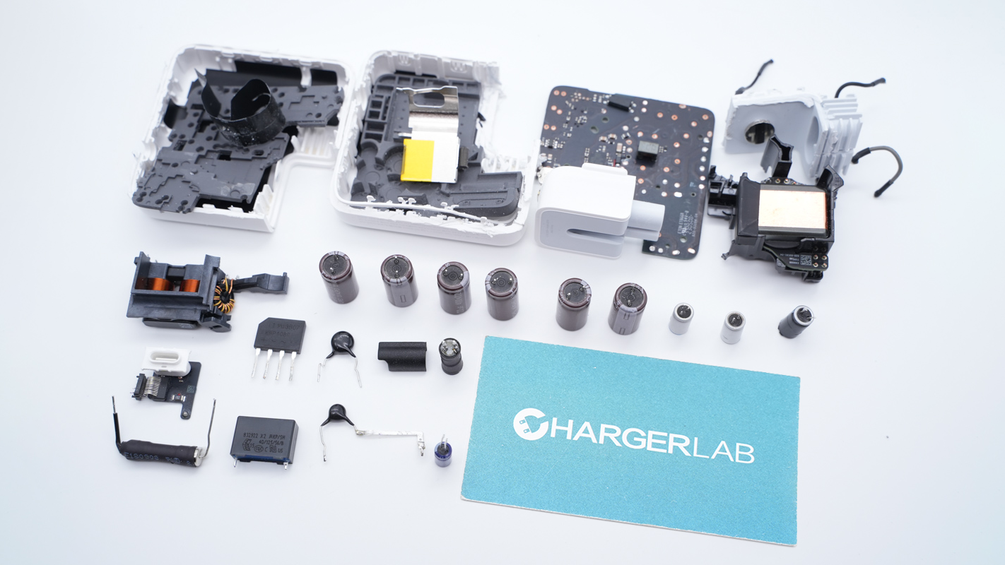
One last look at all the components of this Baseus 100W GaN3 Pro Power Strip.
Summary of ChargerLAB
The Baseus 100W GaN3 Pro Power Strip comes with a standard American plug and a 1.5m (4.9 ft) extension cord for daily use. The power strip has a rated voltage of 125V, current of 10A, and two AC outlets. It can support most fast charging protocols and has four USB ports, making it suitable for charging multiple devices simultaneously, such as laptops and phones.
After taking it apart, we found the gray potting compound and three independent buck circuits can make your charging experience more stable.
This product was originally priced at $99.99, it is now on an 20% discount and is only $79.99. You can click the button at the beginning or the end of the article to get one.
Related Articles:
1. Teardown of Baseus 65W GaN Pro 2C1A Charger (The Third Generation)
2. Teardown of Baseus 67W GaN5 Charging Station (With HDMI Port)
3. Teardown of Baseus 65W GaN5 Pro Fast Charger (2C1A)

