Introduction
Not long ago, AOHi launched a 65W ultra-thin charger, which has a translucent casing. ChargerLAB has introduced many products of AOHi before, and you can click on the link to view them.
ChargerLAB got this charger immediately. And next, we will take a look at the internal components and structure.
Product Appearance
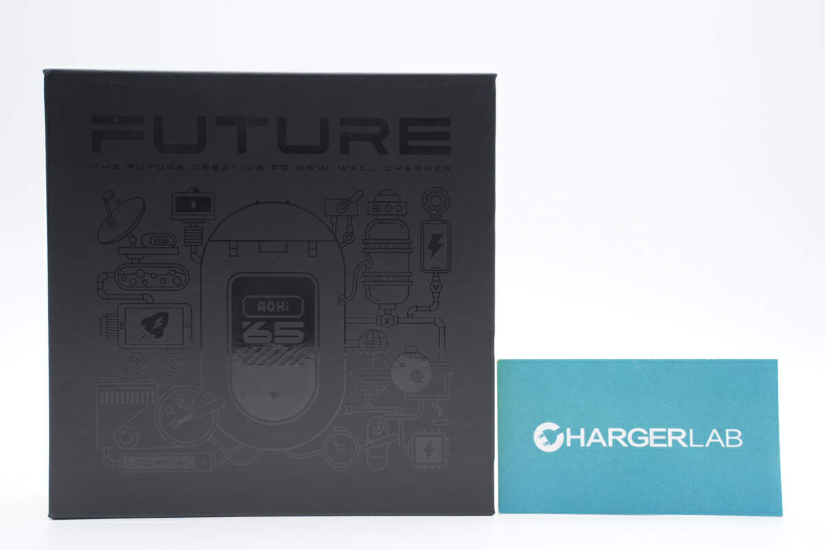
As you can see, the packaging is black in tone.
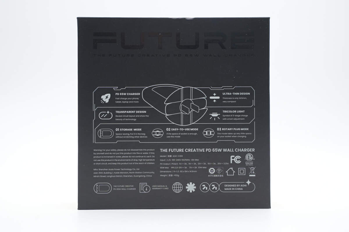
The manufacturer info and selling points are printed on the bottom. I'll introduce the detail below based on the product itself.
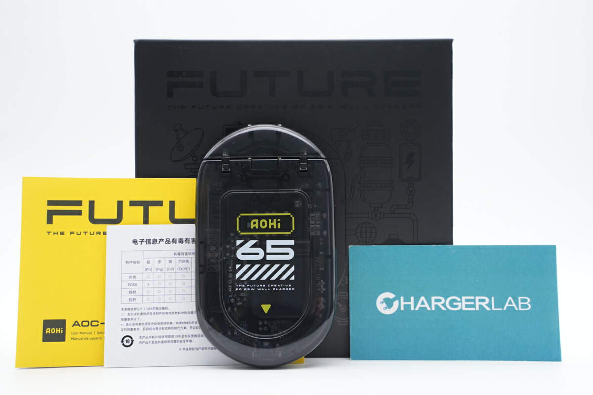
The box contains the charger itself and some documents.
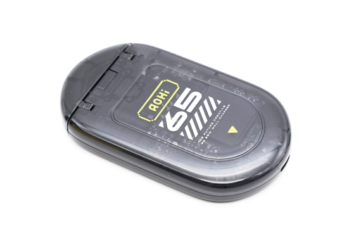
The charger adopts a transparent design.
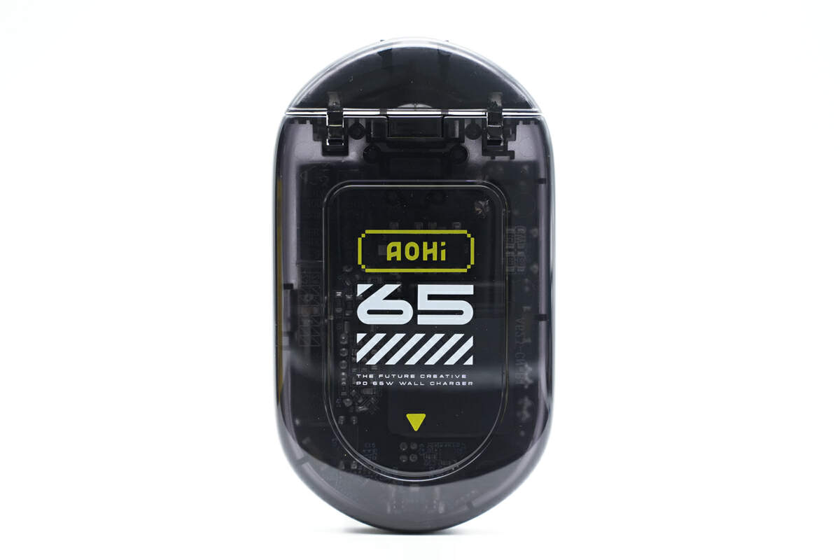
The Aohi logo is printed on the front of the casing. And the USB-C output port is marked with an arrow.
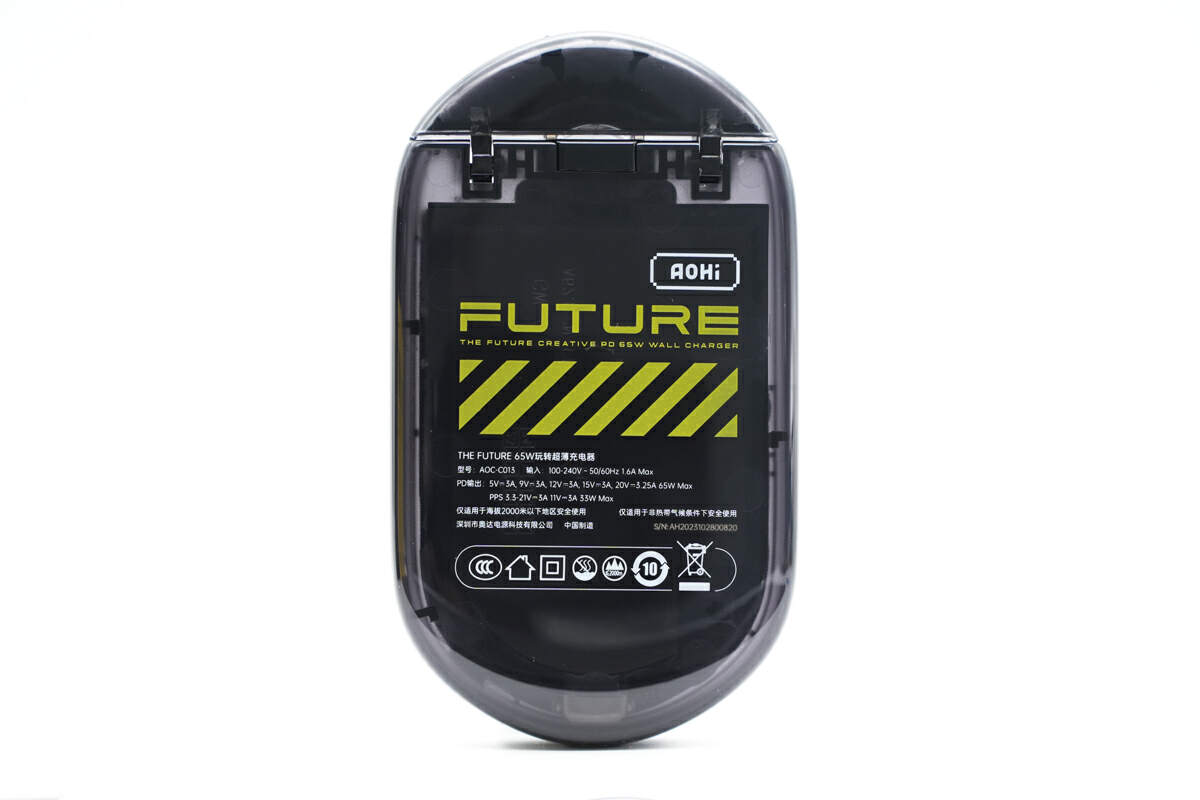
Specs info are printed on the back.

Model is AOC-C013. It can support input of 100-240V~50/60Hz 1.6A. The maximum output is 20V3.25A, which is 65W
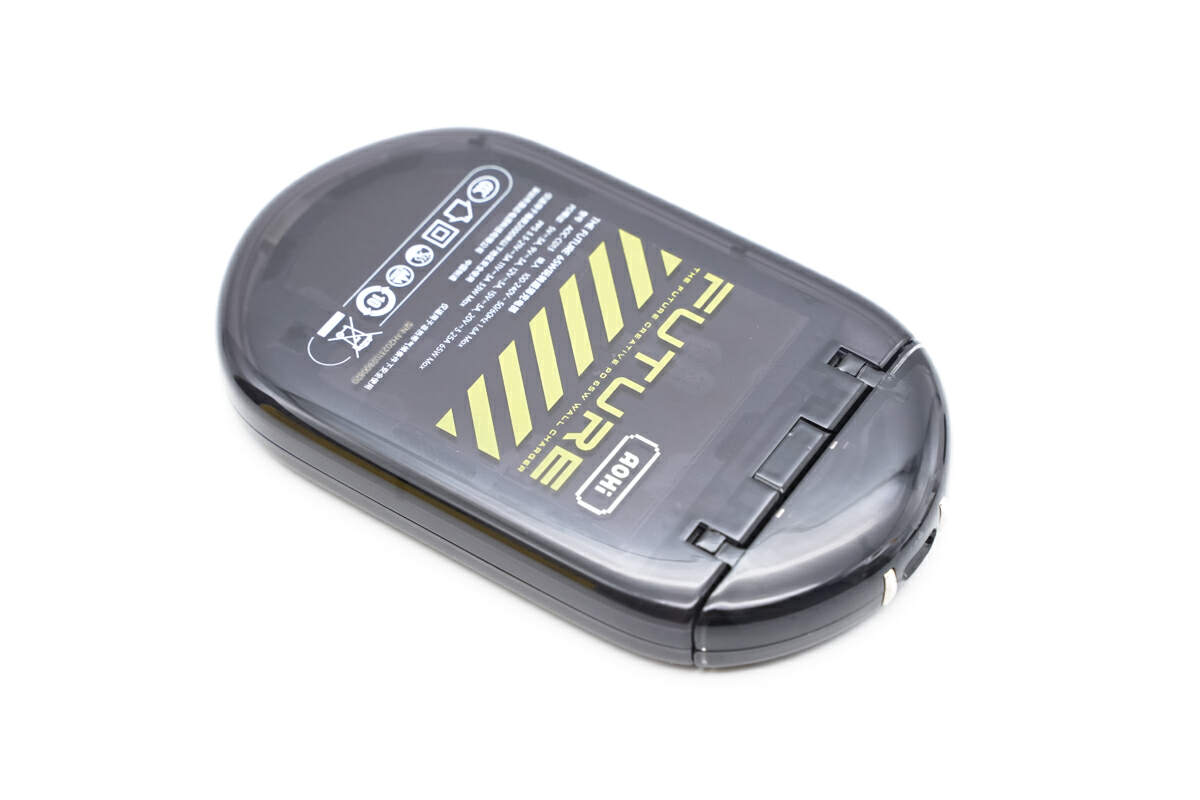
It can hide the prongs inside the casing.
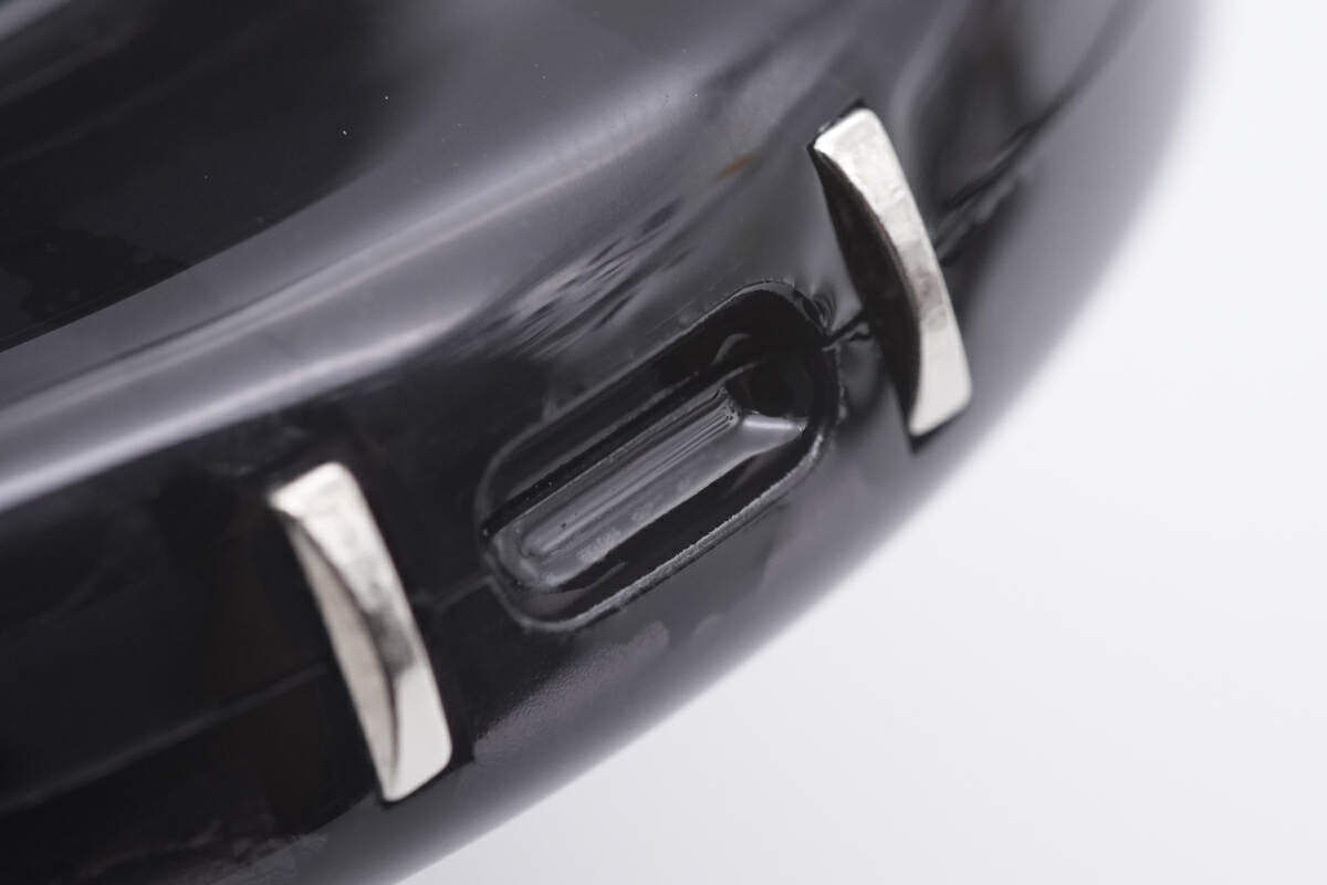
The groove between the two prongs allows the user to unfold the casing easily.
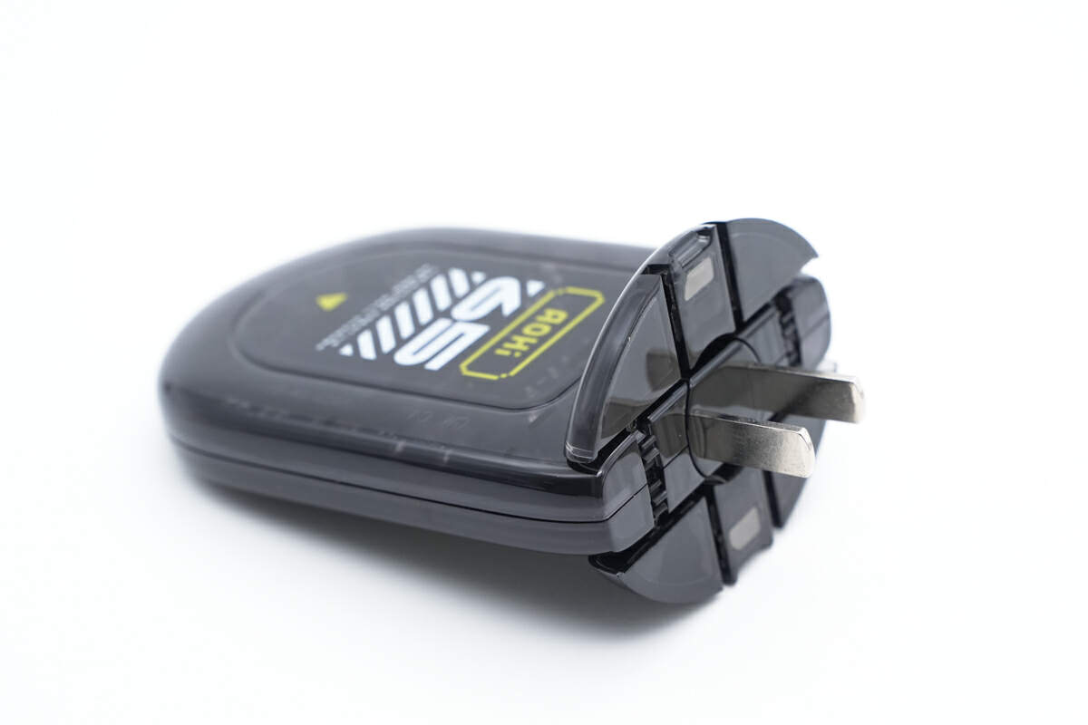
After unfolding, the charger can be plugged stably.
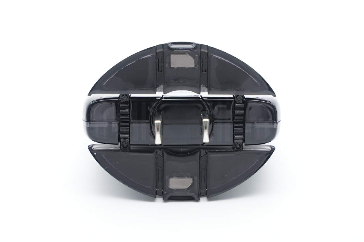
Two magnets are embedded, which can be automatically attracted together when closed.
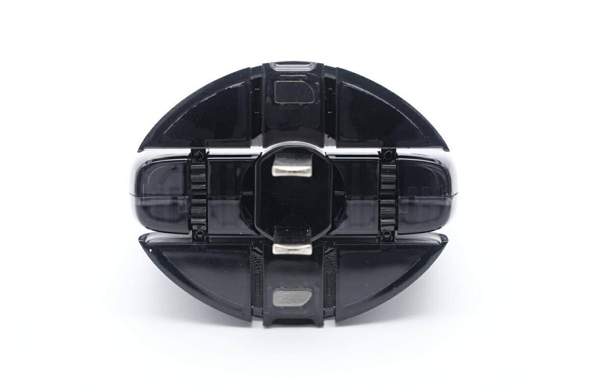
What's more, the prongs can be rotated, which can save space in the socket and make it more flexible to use.
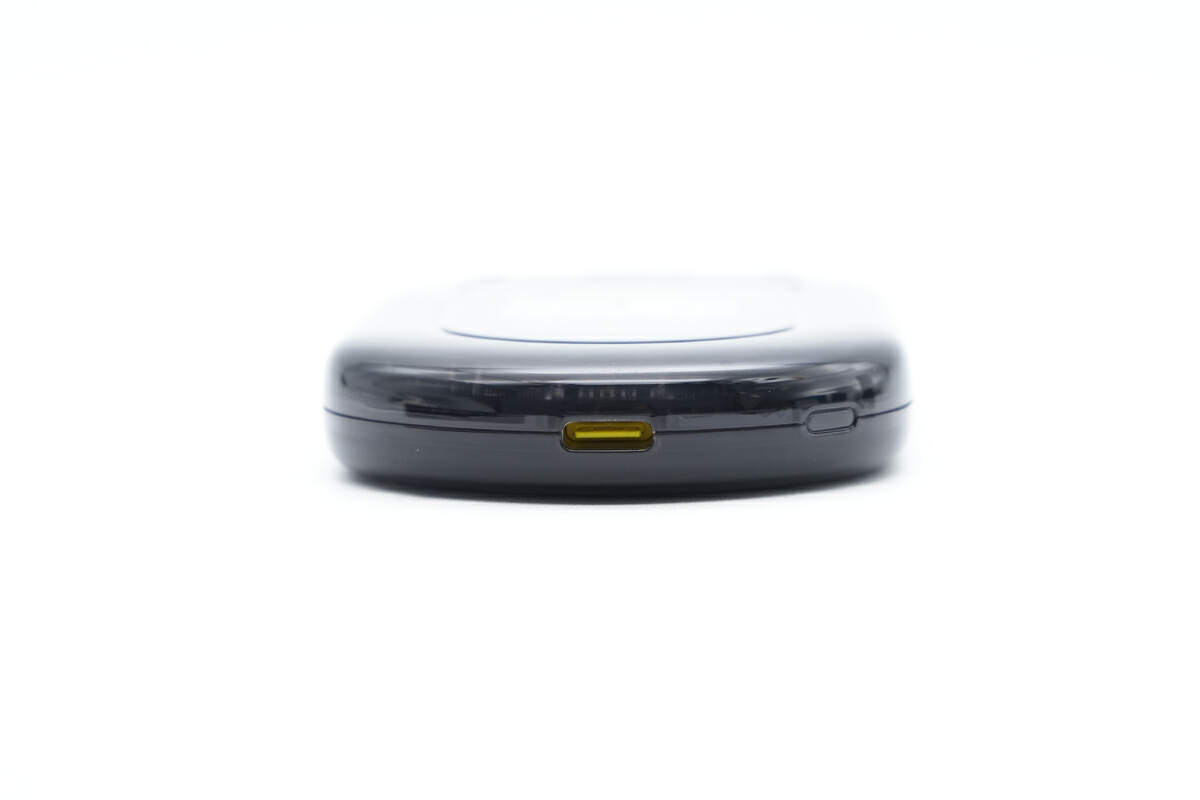
The USB-C has a yellow plastic sheet.
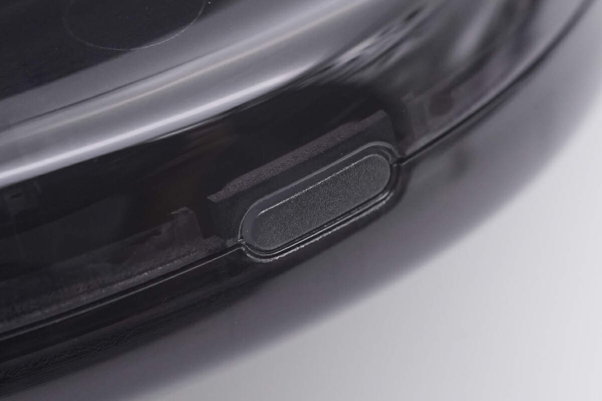
There is an indicator light next to the USB-C.
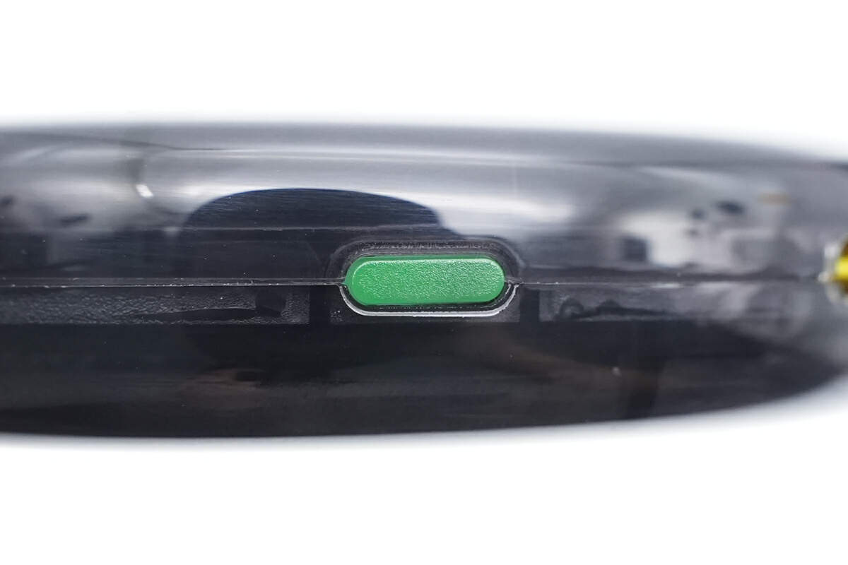
The indicator lights up yellow when fast charging, blue when standard charging, and green when trickle charging.
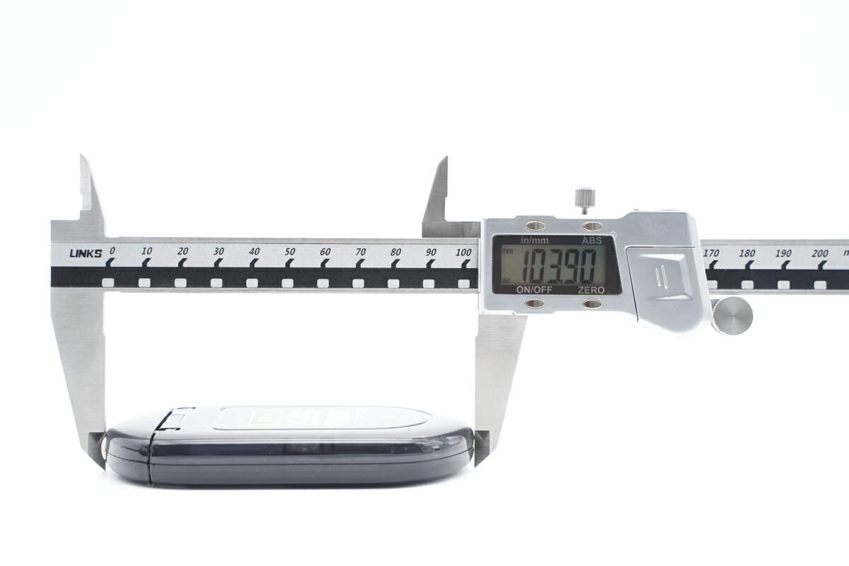
The length of the charger is about 104mm (4.09 inches).
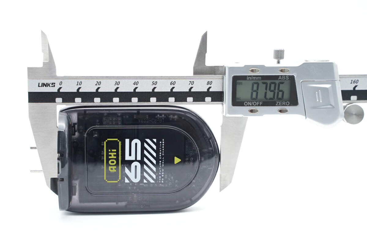
After the casing is unfolding it reduced to about 88mm (3.46 inches).
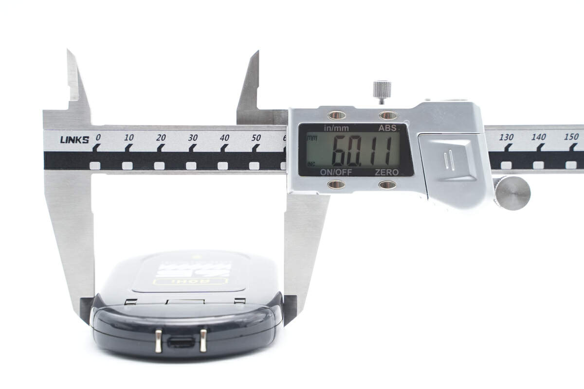
The width is about 60mm (2.36 inches).
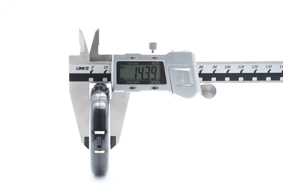
And the thickness is about 14mm (0.55 inches).
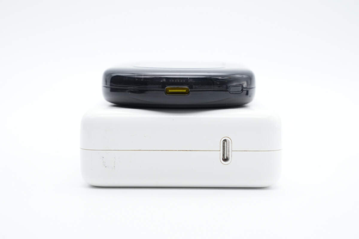
It is only about one-third of Apple's 61W charger in thickness.
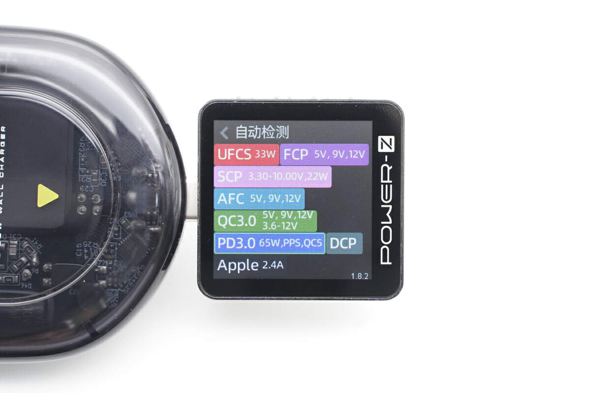
ChargerLAB POWER-Z KM003C shows it can support UFCS, FCP, SCP, AFC, QC3.0/5, PD3.0, PPS, DCP, and Apple 2.4A charging protocols.
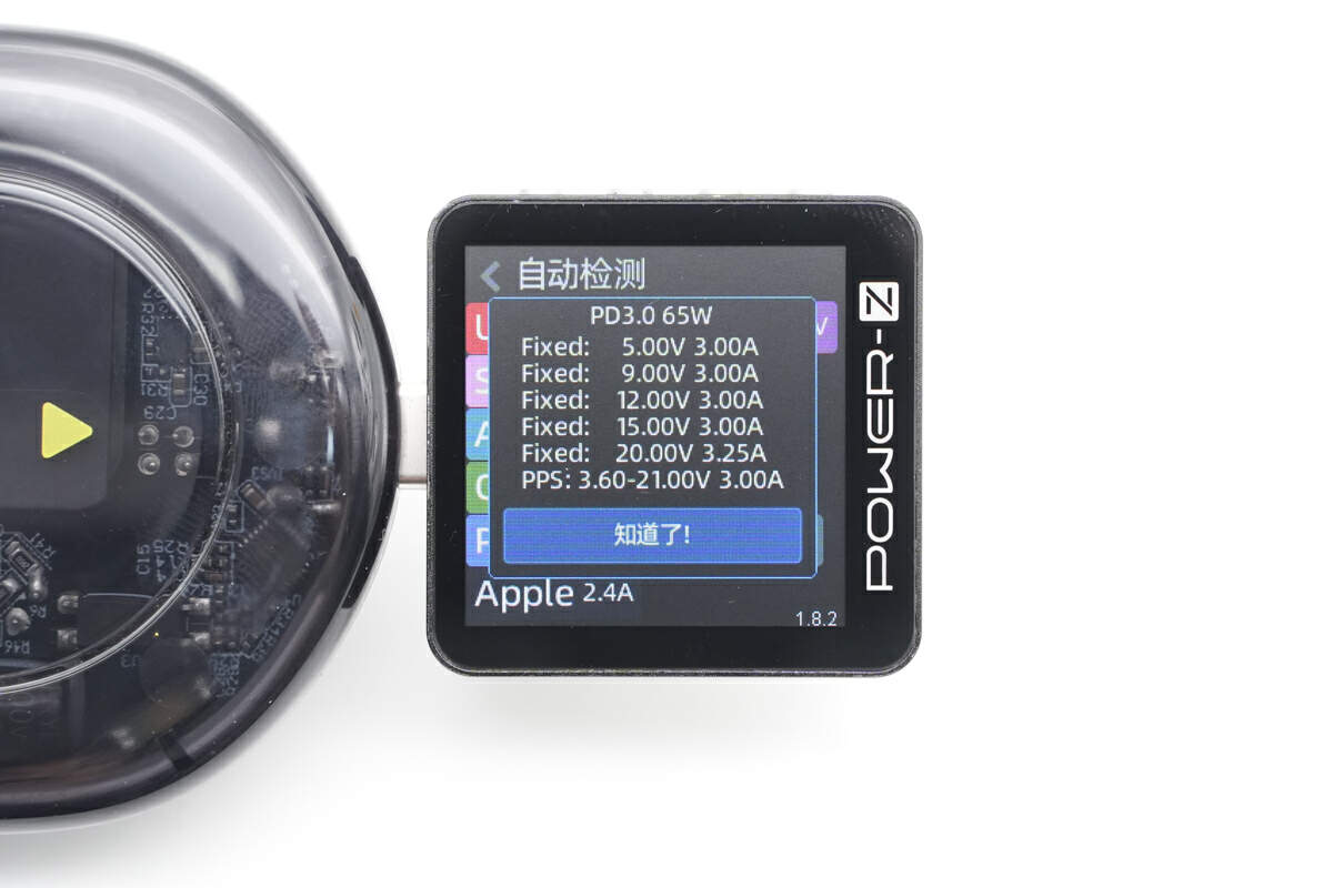
And it has five fixed PDOs of 5V3A, 9V3A, 12V3A, 15V3A, 20V3.25A, and a set of PPS, which is 3.6-21V3A.
Teardown
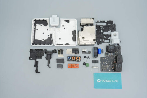
Now comes the exciting part - the teardown.
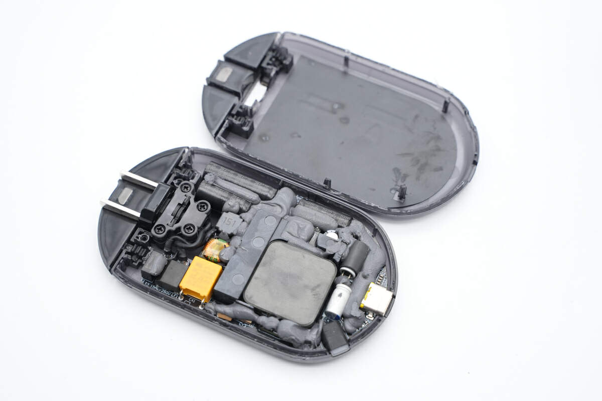
Use a spudger to pry along the gap and open it. A thermal pad is attached to one side of the casing.
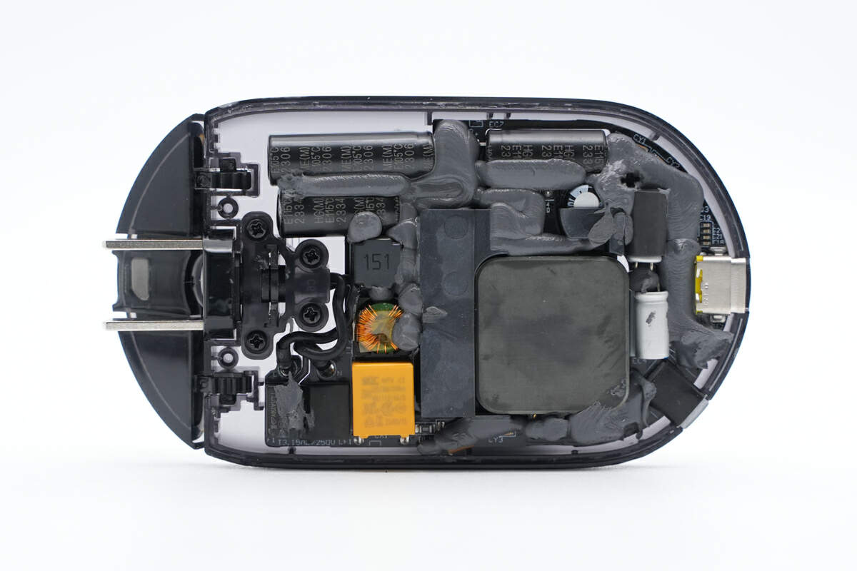
The PCBA module is filled with potting compound to enhance heat dissipation.
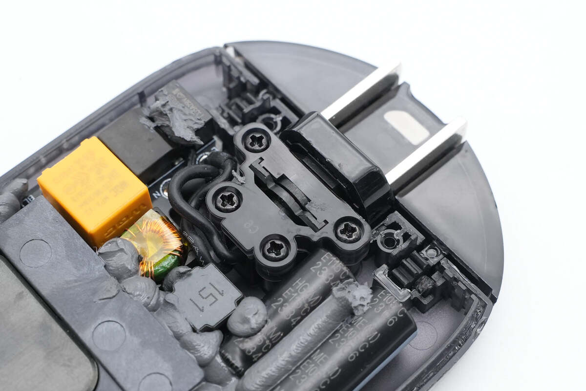
The rotatable prongs are fixed with screws.
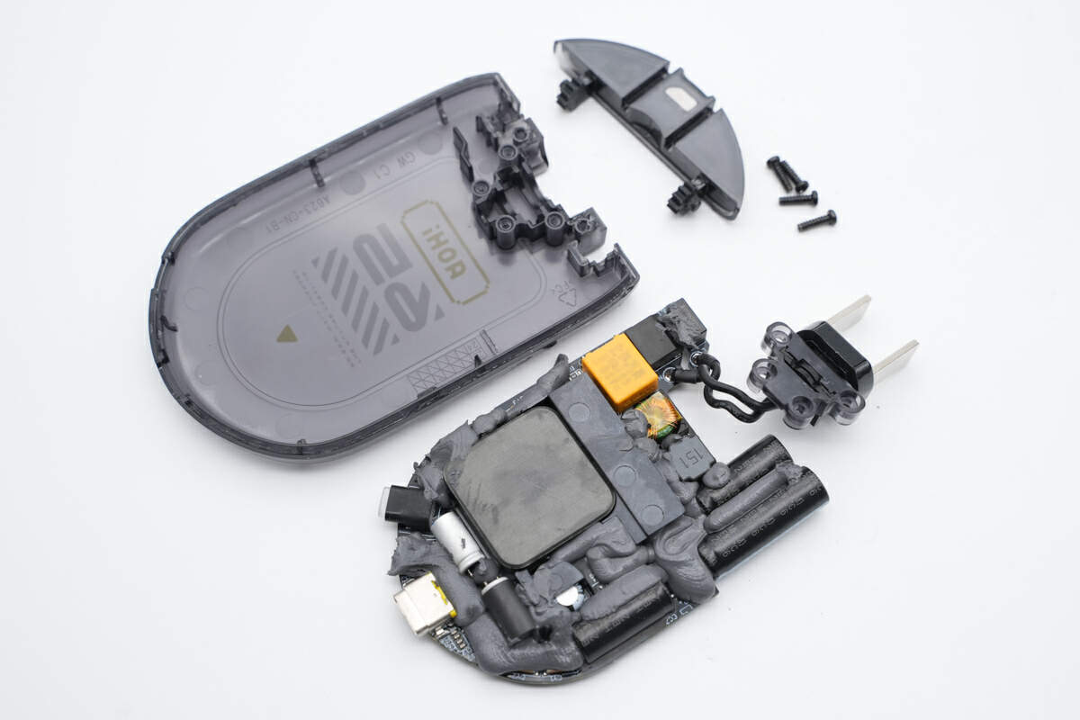
Remove the screws and take out the rotatable pins and PCBA module.
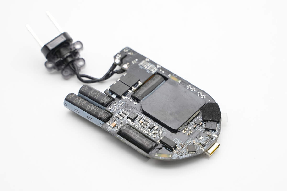
The prongs are connected to the PCBA module by wires.
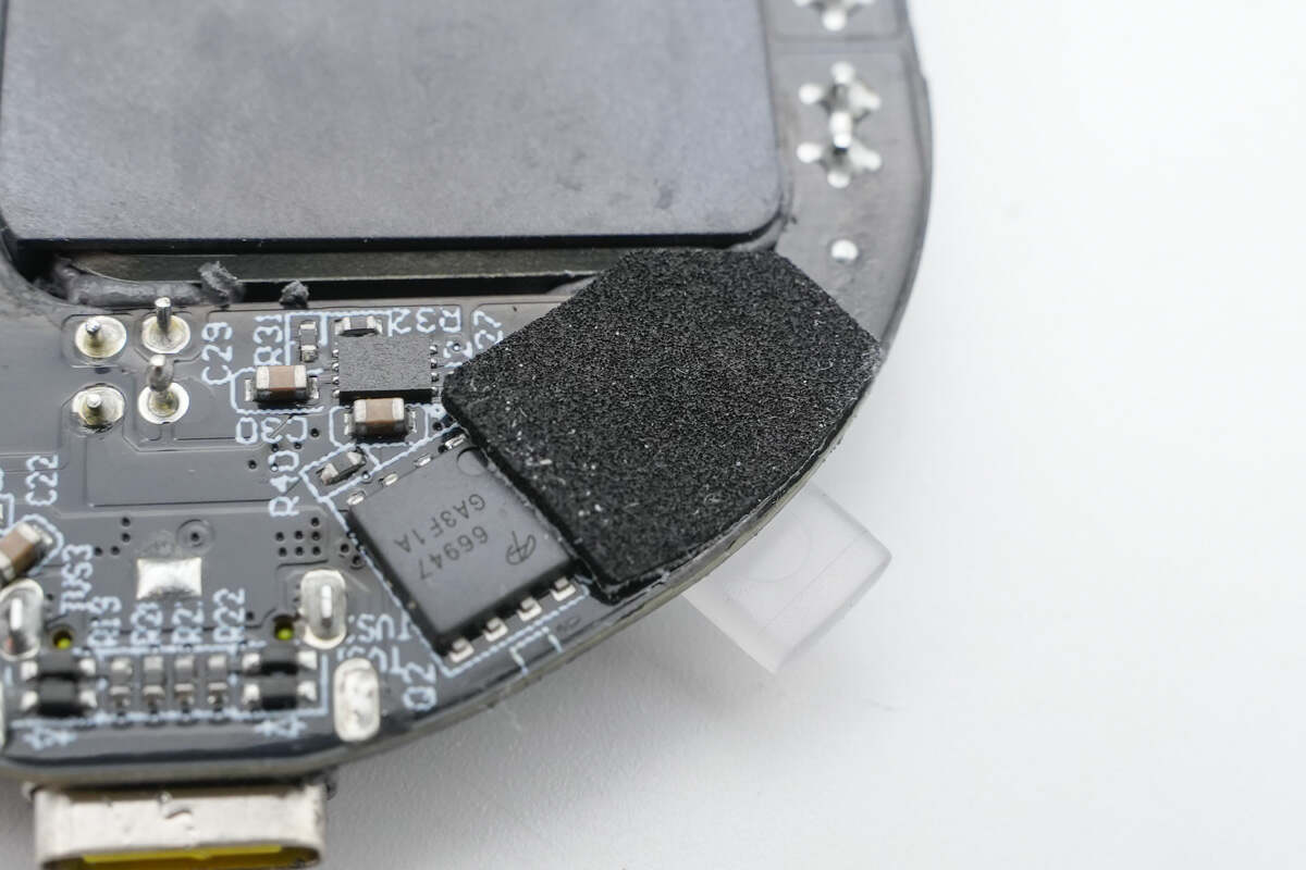
The PCBA module is pasted with black foam to avoid light leaks.
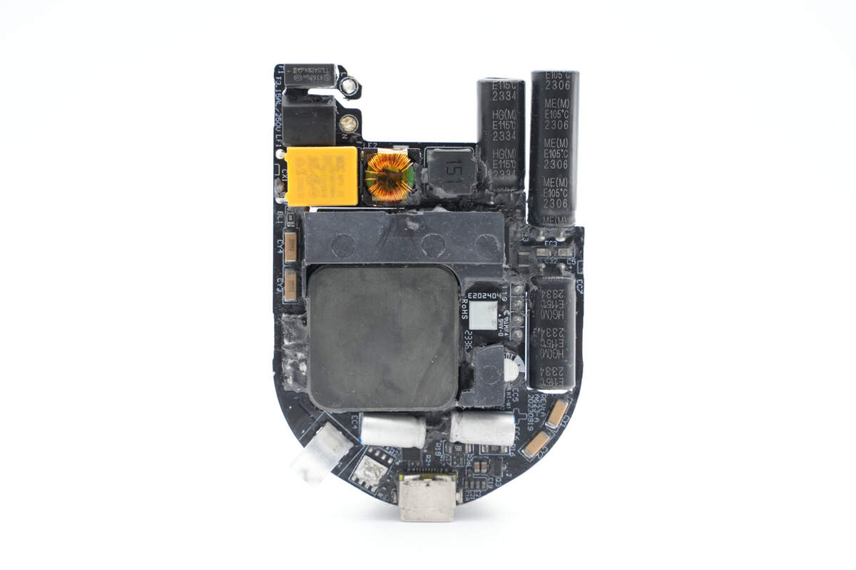
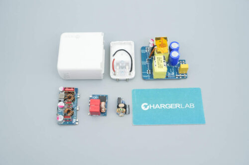
The AC input end, fuse, common mode choke, electrolytic capacitor for input filtering, and planar transformer are all on the front of the PCBA module.
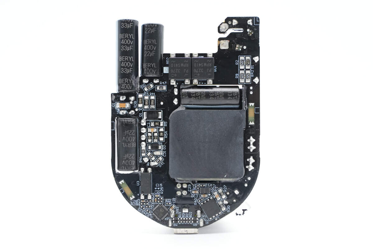
The electrolytic capacitor for input filtering and planar transformer are the same as seen before. And the synchronous rectifier controller, synchronous rectifier MOSFET, and protocol chip are all on the back of the PCBA module.
The charger uses a Silergy chip and a synchronous rectifier controller to form a flyback topology. It outputs a wide voltage range, which is adjusted by the protocol chip through a feedback optocoupler. Next, we will introduce each component, starting with the input end.
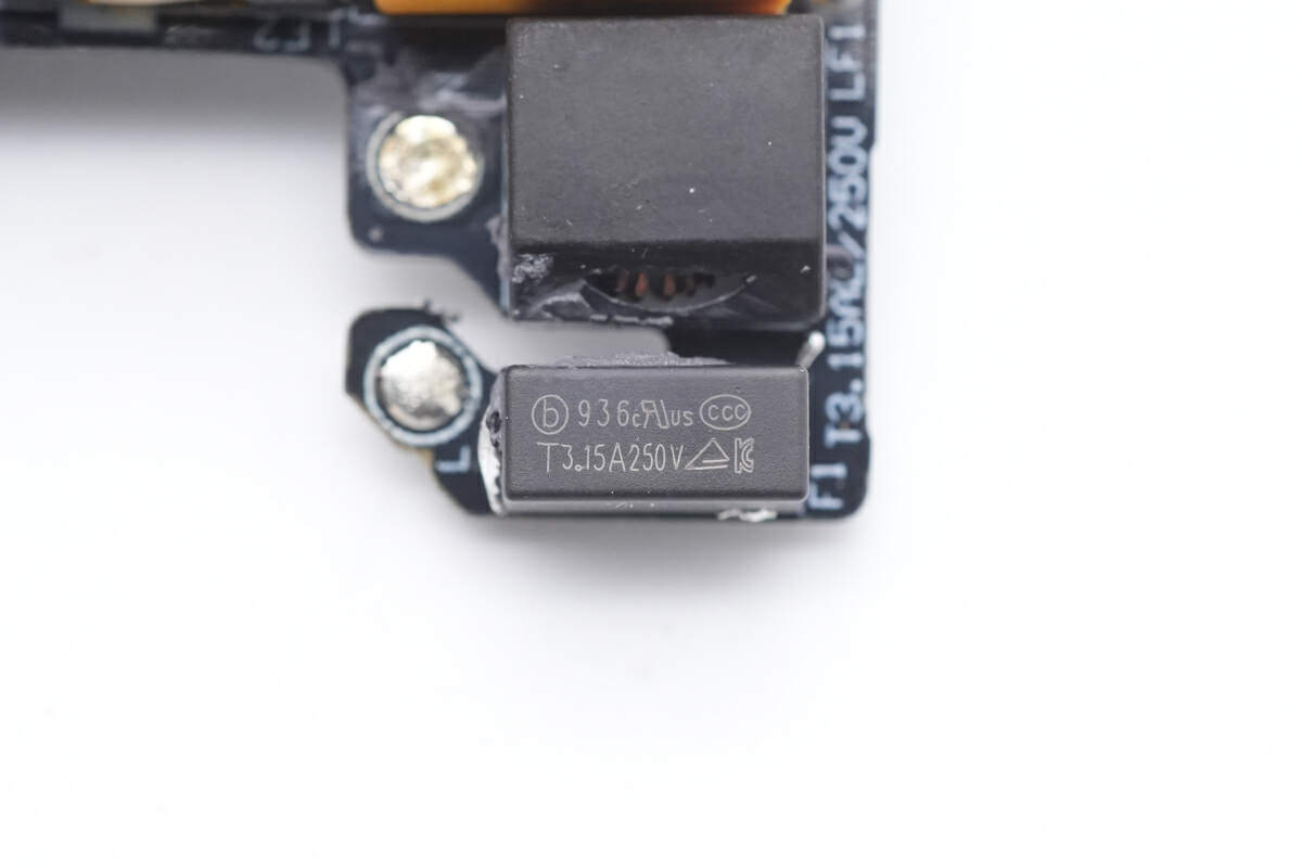
The input fuse marked with 936 is from Betterfuse. 3.15A 250V.
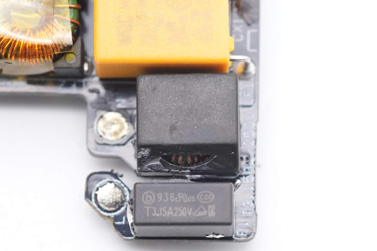
The common mode choke is SMD type.
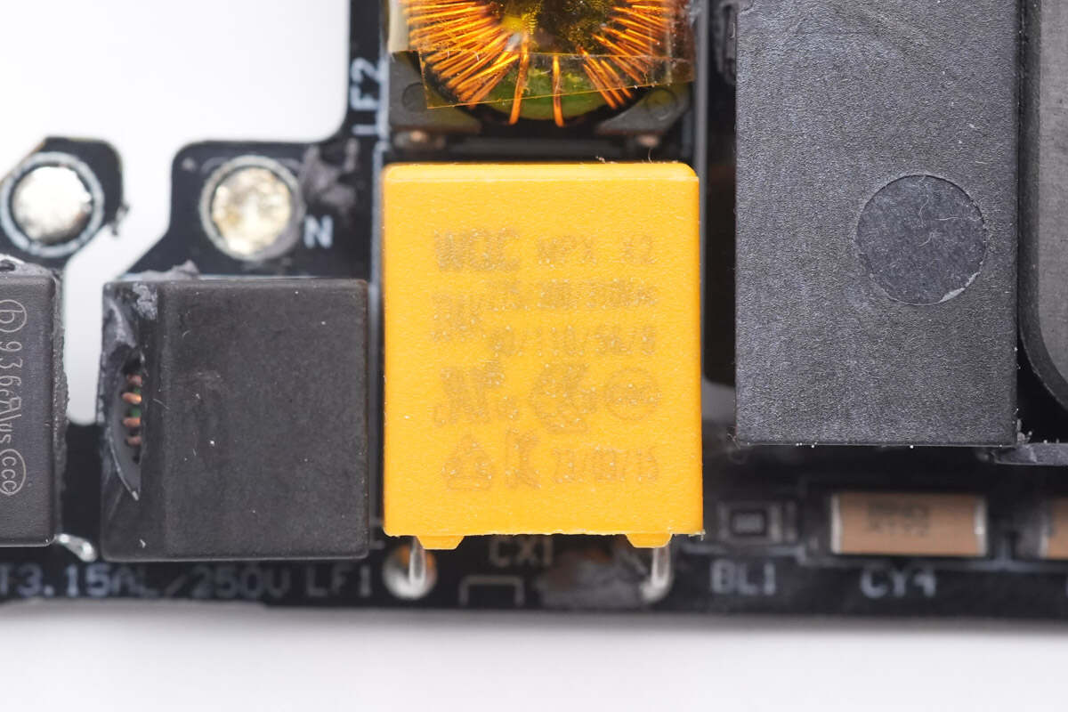
The X2 safety capacitor is from WQC. 0.33μF.
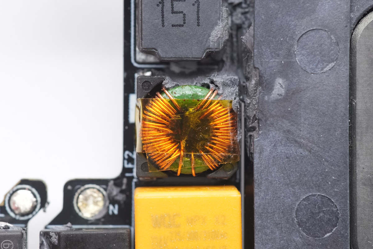
The other common mode choke is wound with magnet wires, and it is also SMD type.
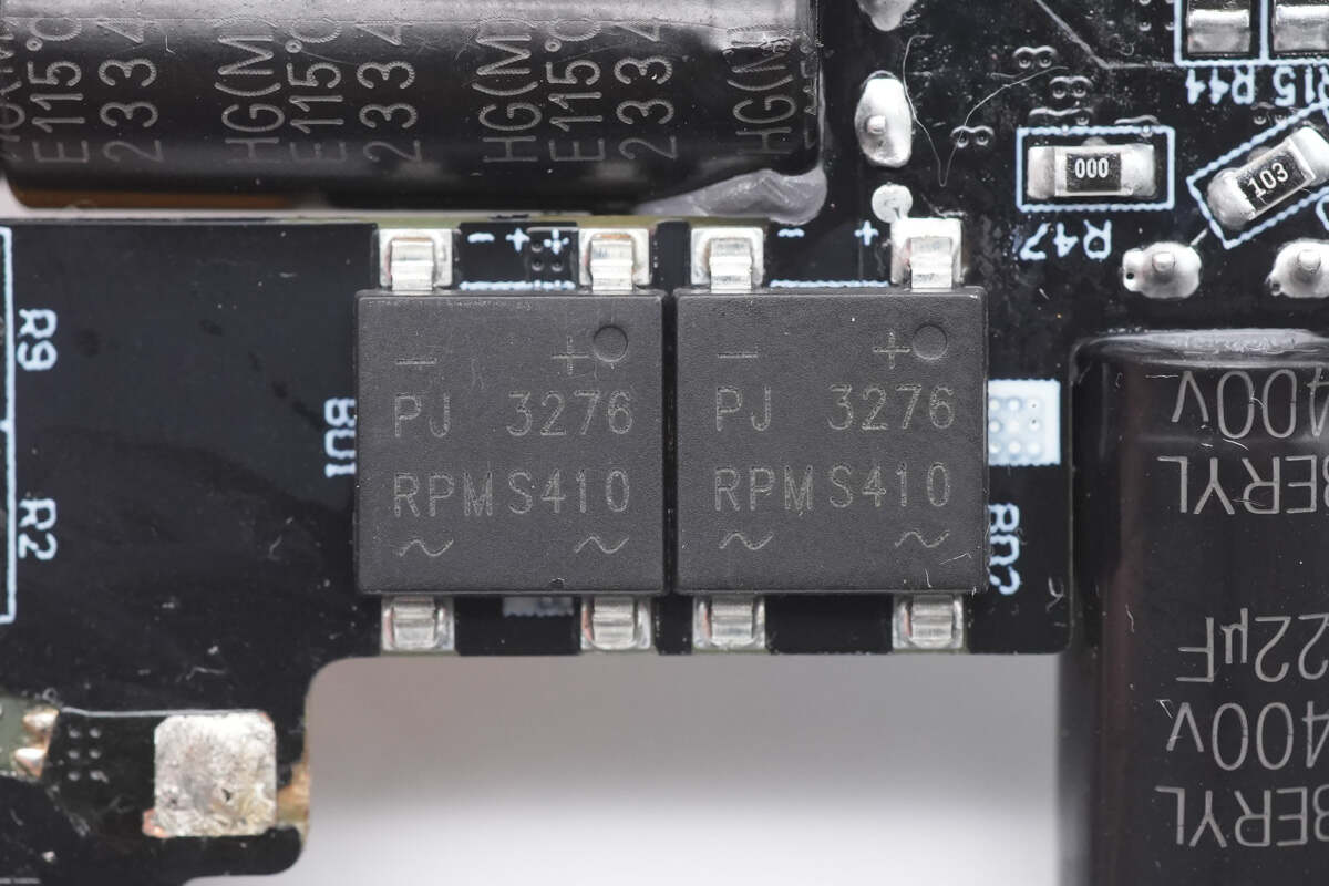
Two PANJIT bridge rectifiers are connected in half-bridge, which can dissipate heat evenly. Model is RPMS410. 4A 1000V.
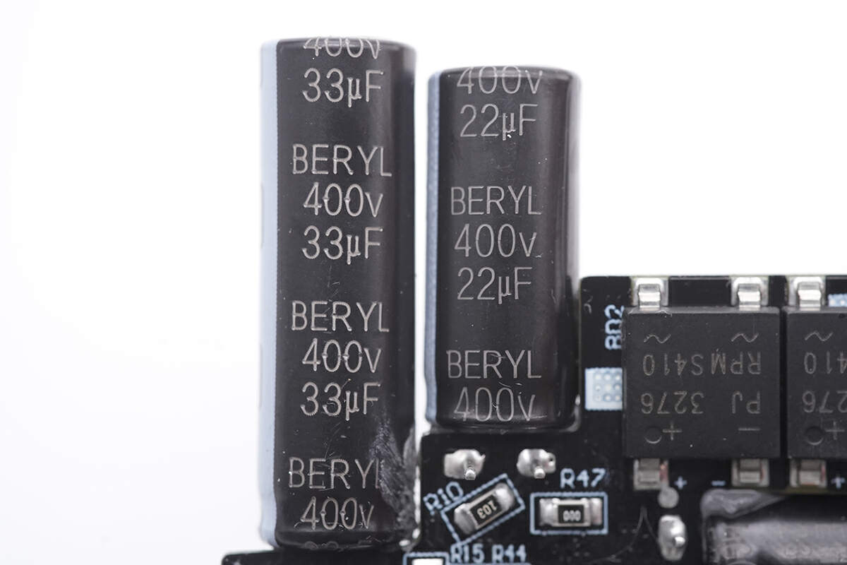
The two high-voltage electrolytic capacitor for input filterings are from Beryl, and the specifications are 400V33μF and 400V22μF.
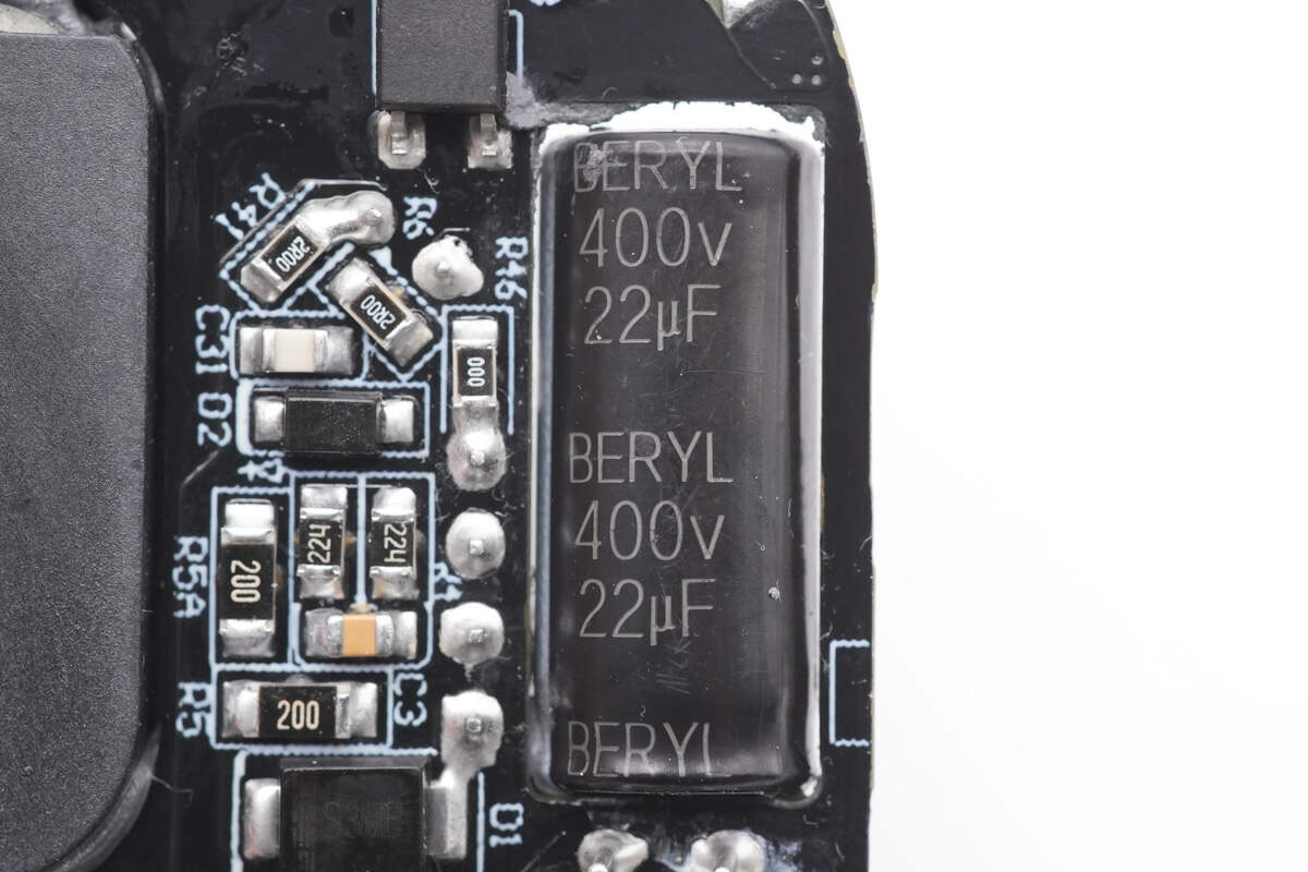
The other high-voltage electrolytic capacitor for input filtering is also 400V22μF.
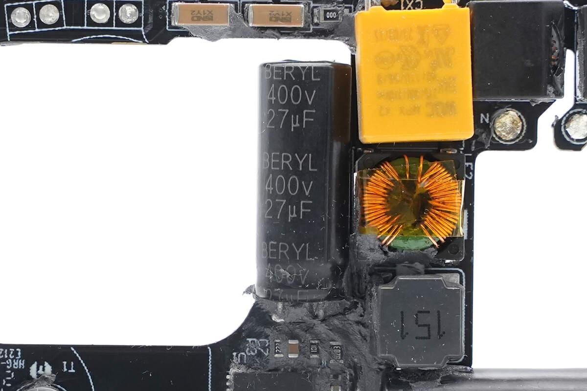
The last one is 400V27μF, so the total capacity is 104μF.
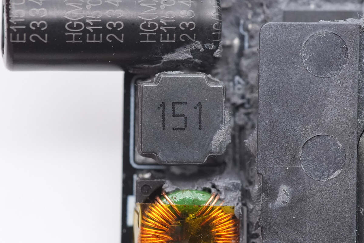
The differential mode chock is marked with 151.
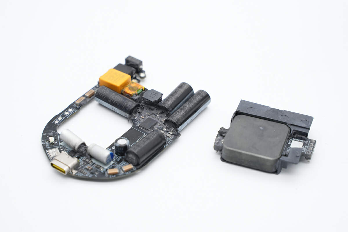
Remove the planar transformer.
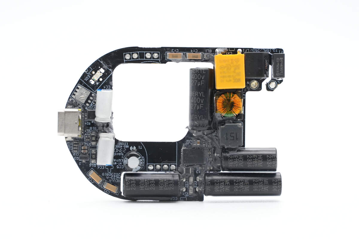
And the master control chip is in the middle of the four electrolytic capacitors.
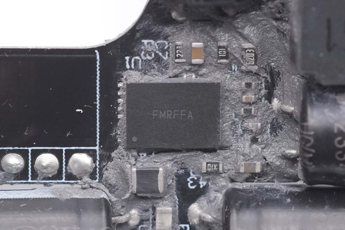
The GaN master control chip is from Silergy and is marked with FMRFFA.
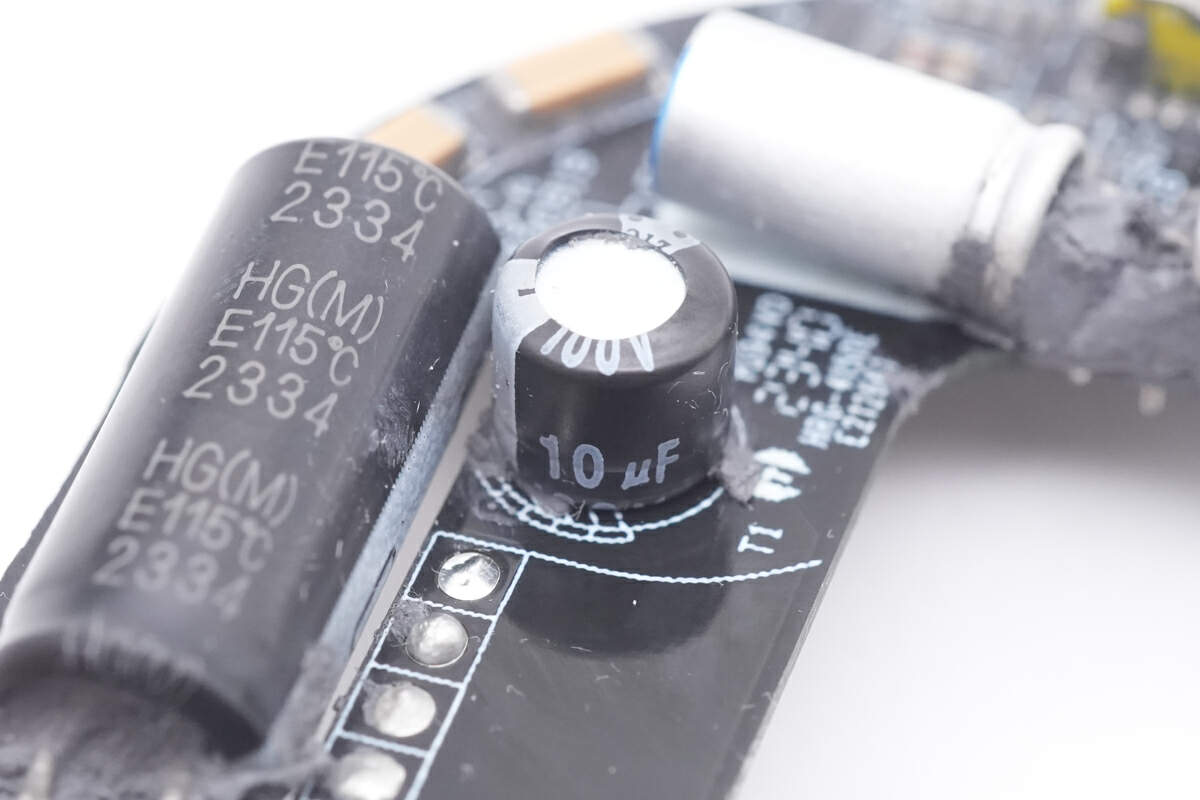
This is the electrolytic capacitor for input filtering that powers the master control chip. 10μF100V.
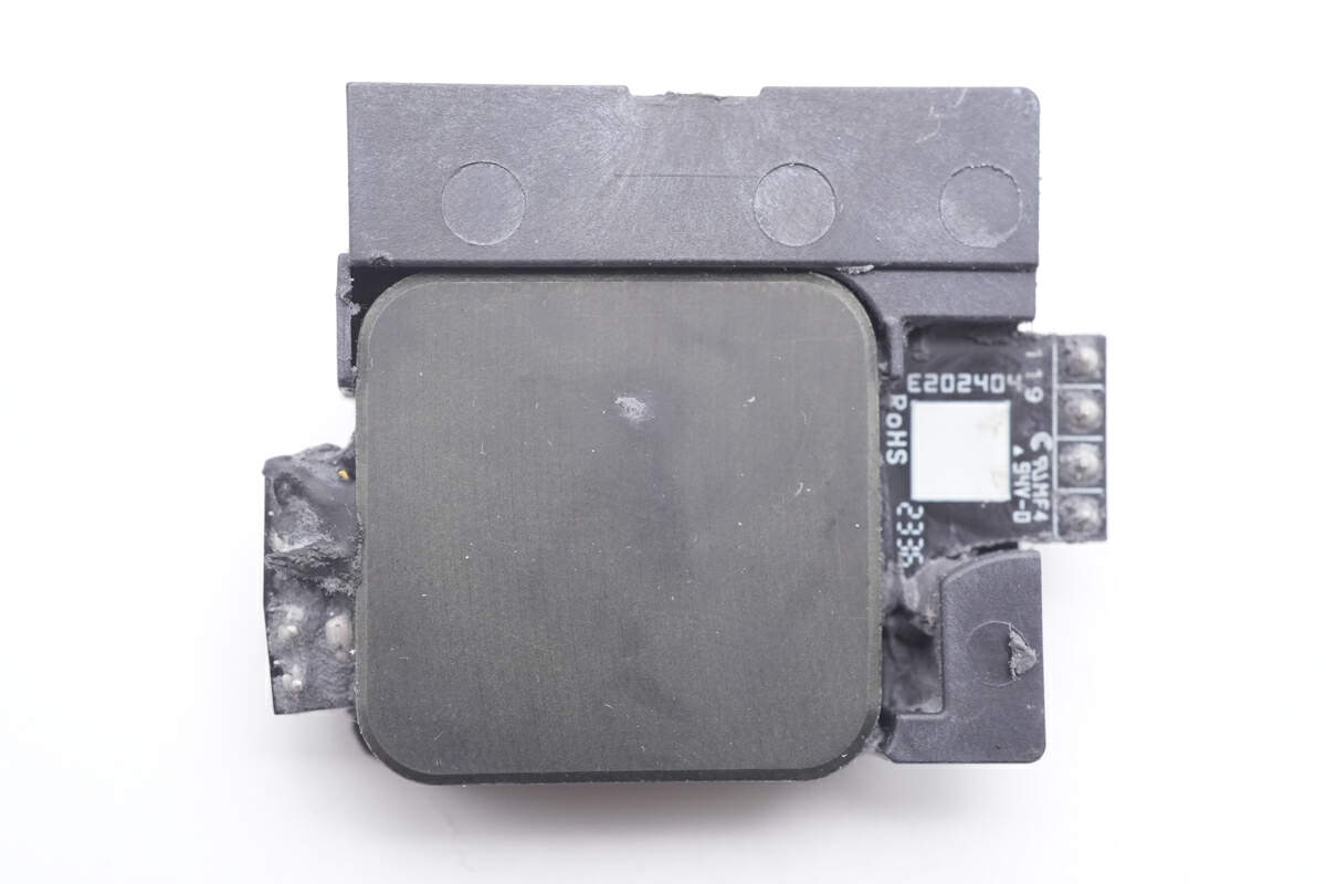
The planar transformer is insulated by a plastic frame.
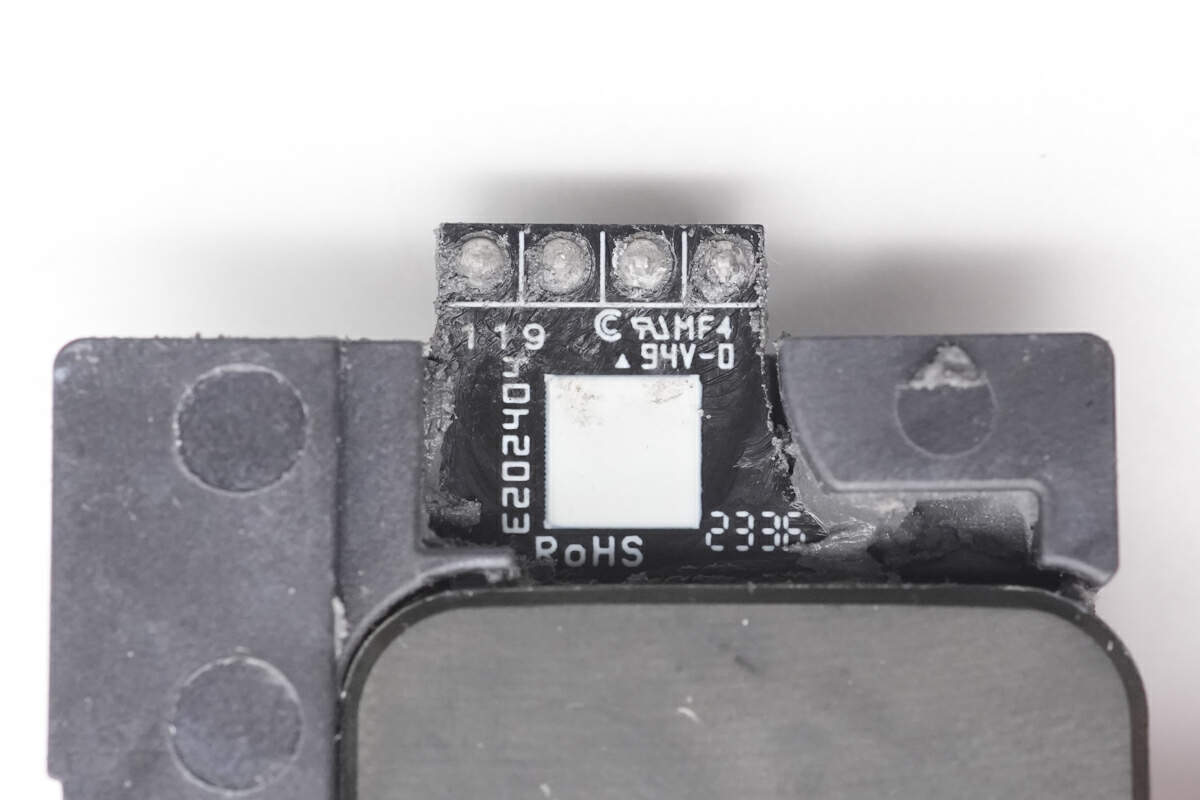
And it is from Techigh.
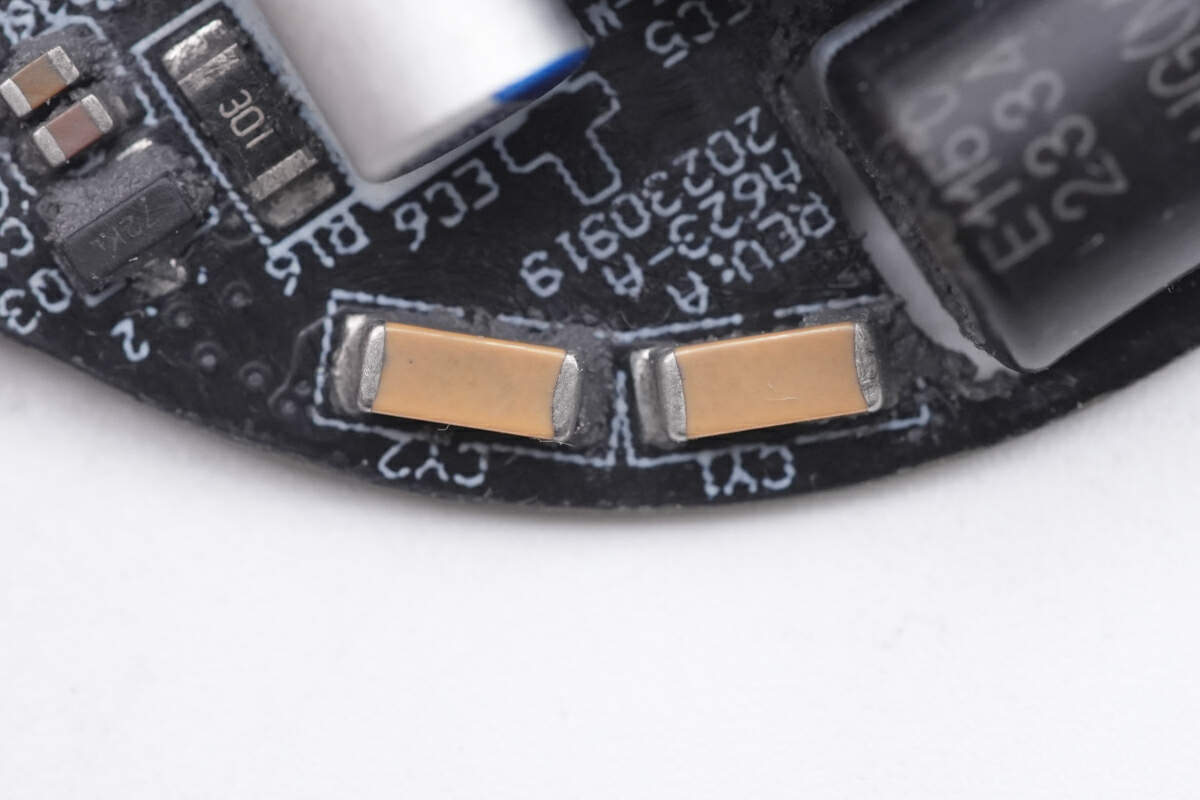
There are two SMD Y capacitors on the side of the PCBA.
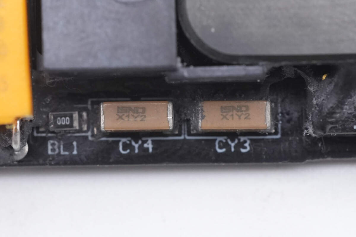
The other two SMD Y capacitors are from ISND. They are connected in series.
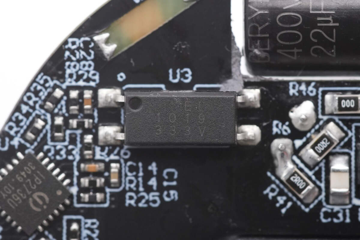
The optocoupler marked with EL1019 is from Everlight and is used for output voltage feedback regulation.
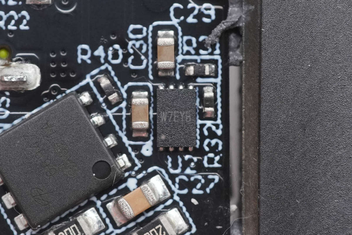
The synchronous rectifier controller is also from Silergy. It supports QR flyback and ZVS flyback topology. And it has adaptive gate voltage control and adopts DFN2 x 3-8 package. Model is SY5238.
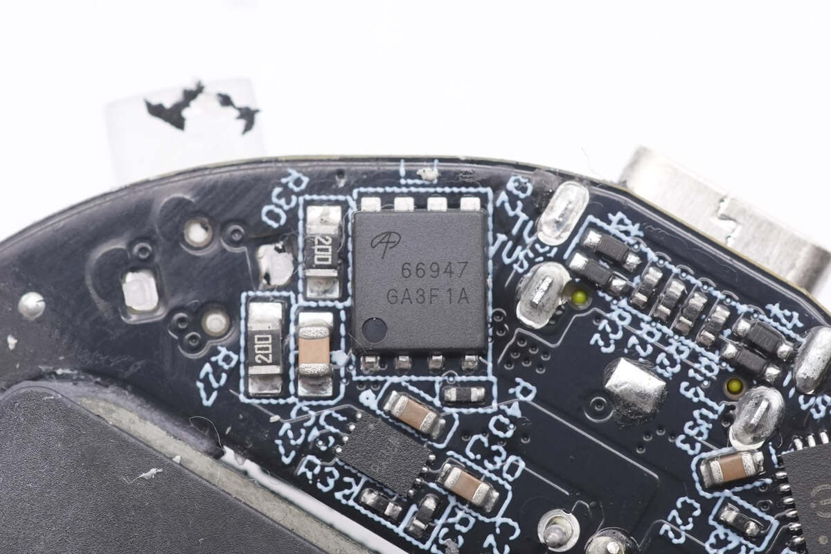
The synchronous rectifier is from AOS and adopts DFN5 x 6 package. Model is AONS66947. 100V 2.9mΩ.
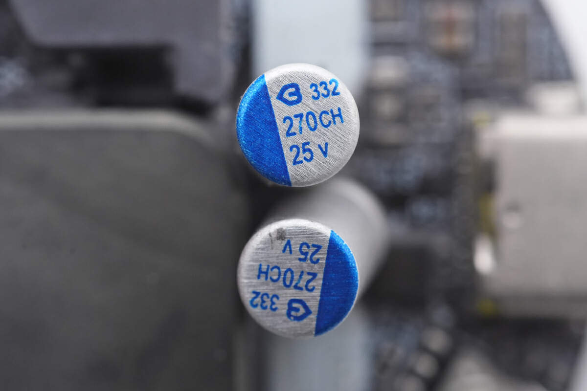
Two solid capacitors for output filtering are from Beryl CH series. 220μF25V.
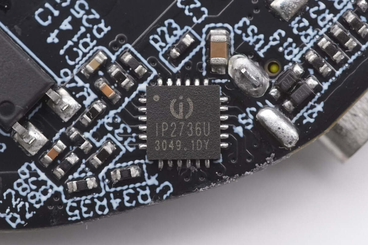
The protocol chip is from Injoinic and is used for USB ports. It supports PD3.1/PPS/EPR 28V, QC5/4+/3+/3.0/2.0, and SAMSUNG 2.0A fast charging protocols. Model is IP2736U.
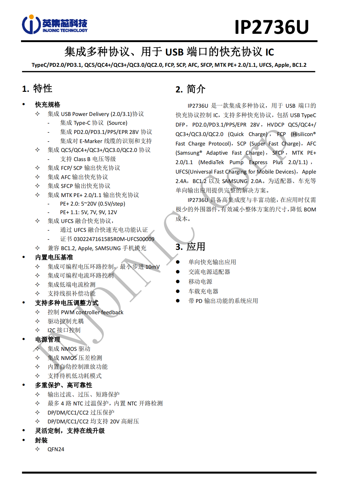
Here is all the information about the Injoinic IP2736U.
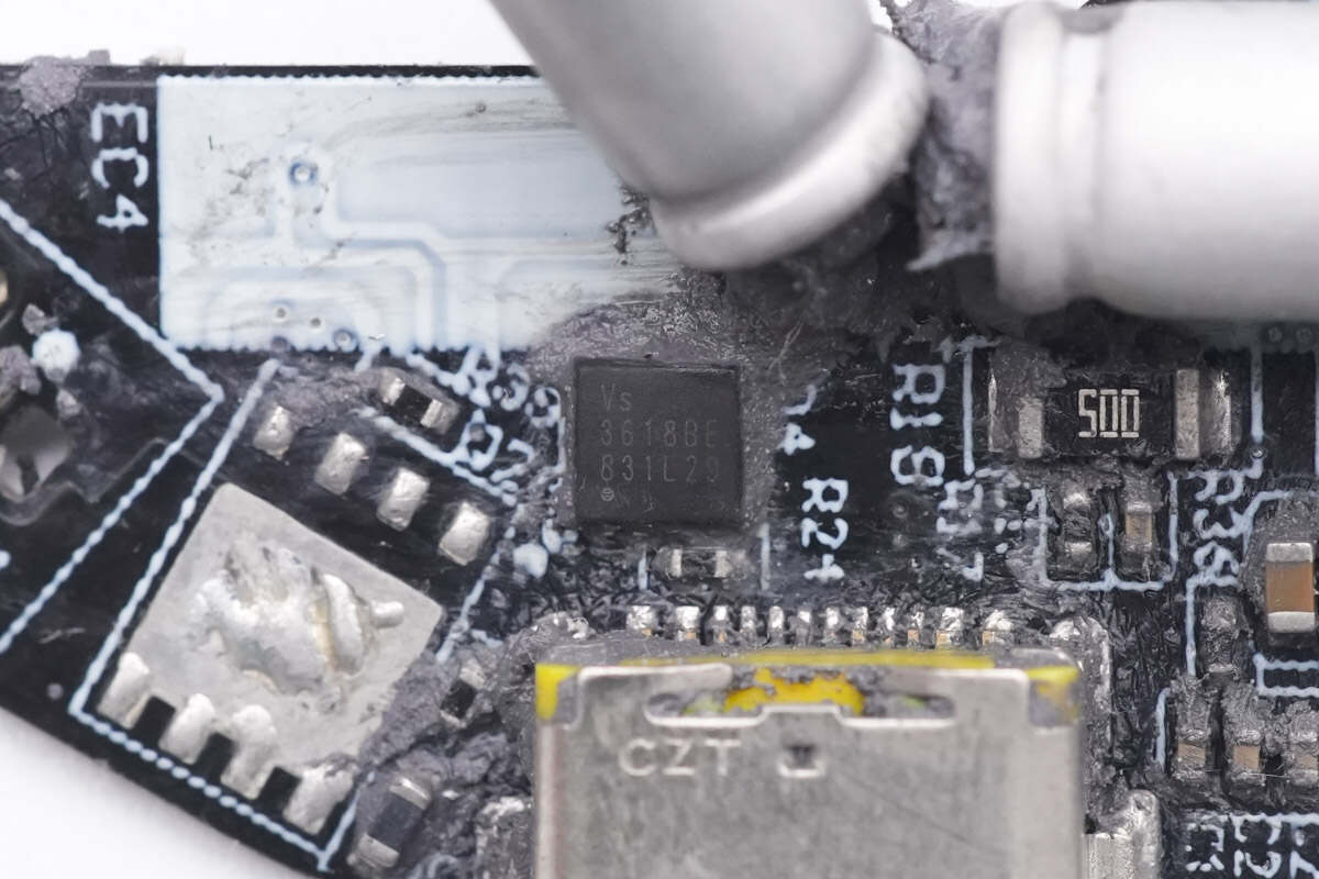
The VBUS MOSFET is from Vergiga Semi, and it adopts PDFN3333 package. Model is VS3618BE. 30V 5.2mΩ.
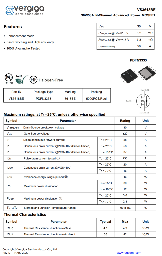
Here is all the information about the Vergiga Semi VS3618BE.
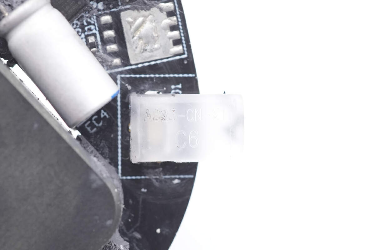
The indicator light has a translucent plastic.
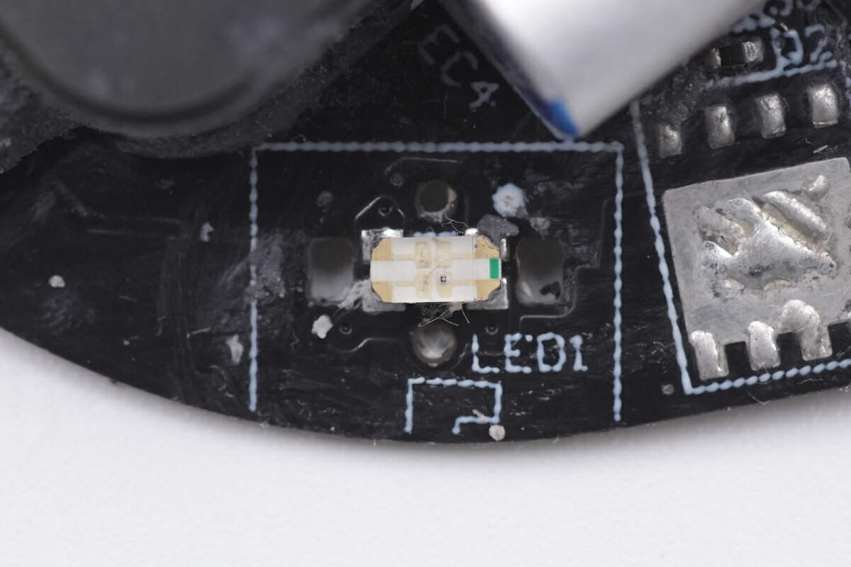
The SMD LED indicator is used to show charging status.
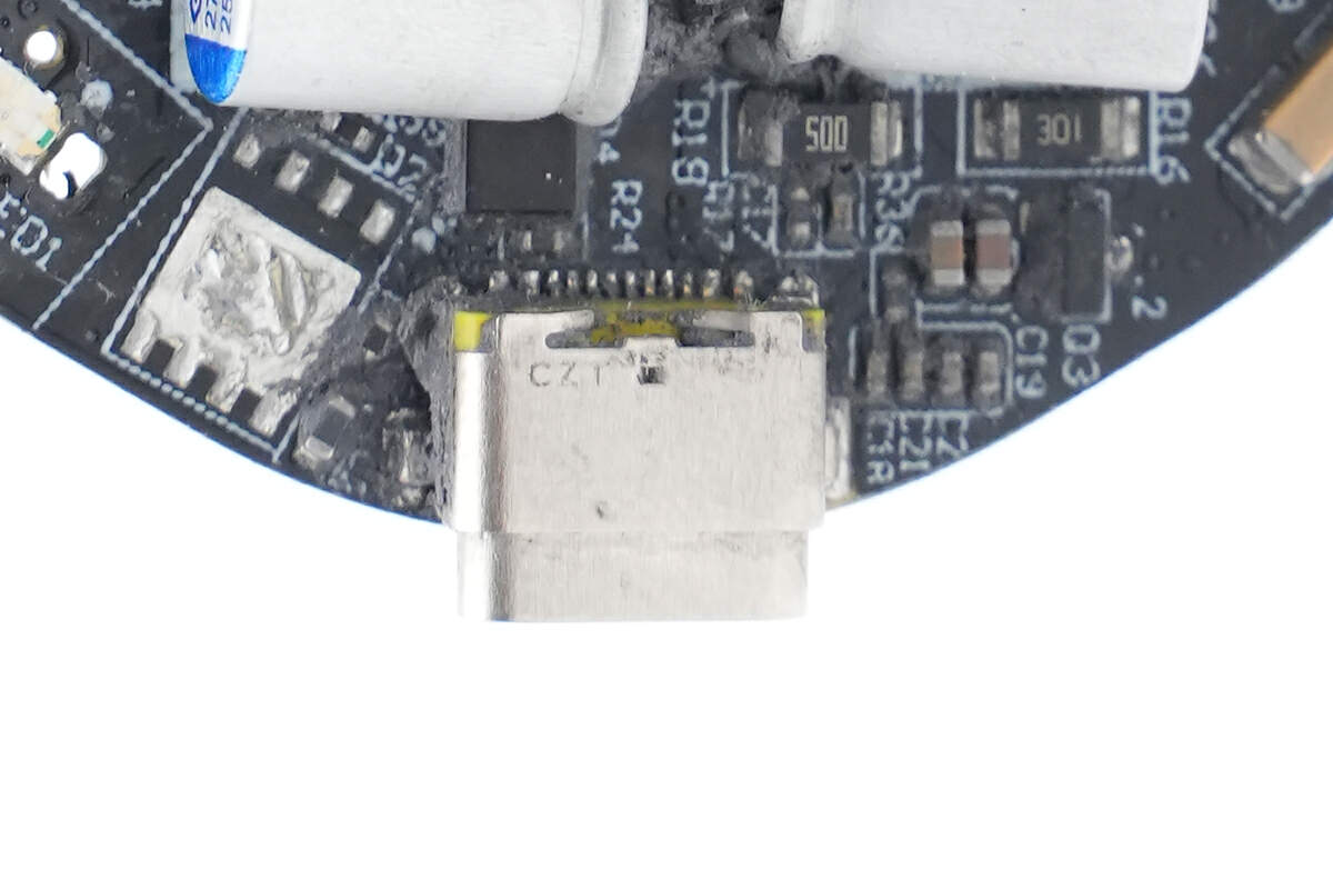
The USB-C socket is from CZT.
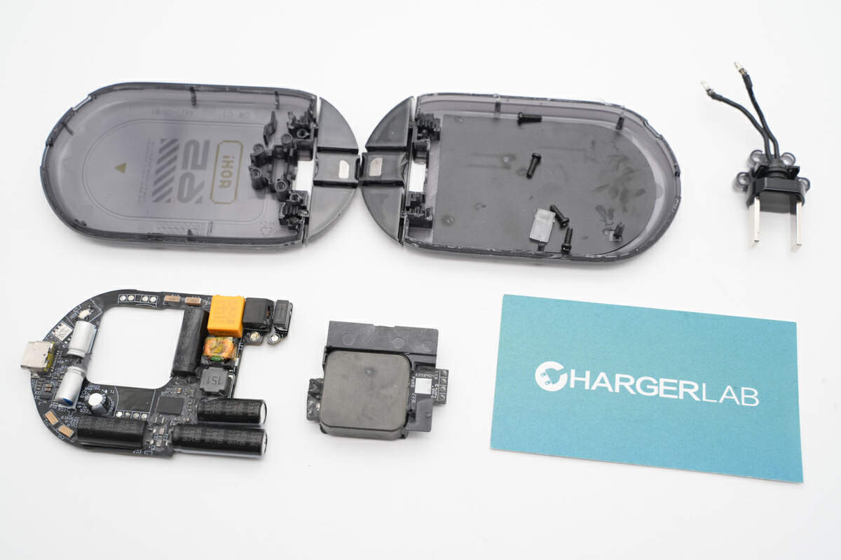
Well, that's all components of the charger.
Summary of ChargerLAB
This charger from AOHi adopts a translucent design, which is pretty cool. The foldable prongs can be rotated, which can make it more flexible to use. And the internal PCBA module is hollowed out to place a planar transformer and the high-voltage electrolytic capacitor for input filtering to reduce the thickness.
Its maximum output in PD mode can reach 65W. But under the PPS protocol, the highest power only reaches 33W.
If you need an ultra-thin charger to save space, this charger is for you.
Related Articles:
1. Ultra-Slim & GaN | Teardown of Baseus 65W Charger (1A1C)
2. Put It Into Pocket | Teardown of TEGIC 65W Ultra Thin Charger
3. Teardown of Realme 50W Mini SuperDart Charger (Ultra-thin)

