Introduction
ANKER has launched a 200W desktop charging station, which belongs to the Anker Prime series. It has four USB-C ports and two USB-A ports. The four USB-C ports all support 100W output power, the USB-A ports support 22.5W output power, and it supports intelligent output power distribution.
It supports an input voltage of 100~240V. It can charge laptops, tablets, phones, and headphones at the same time. Next, let's take it apart to see its internal components and structure.
Product Appearance
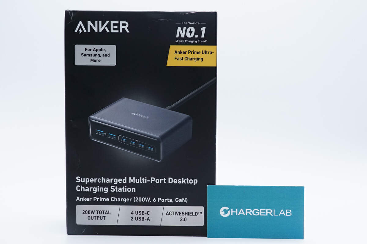
The packaging box is black and is printed with ANKER, product name, product appearance, and selling points.
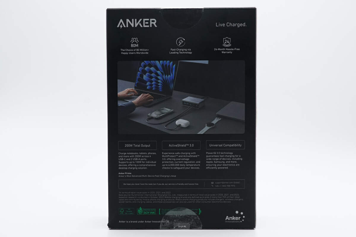
The back is printed with information such as usage scenarios and output power.
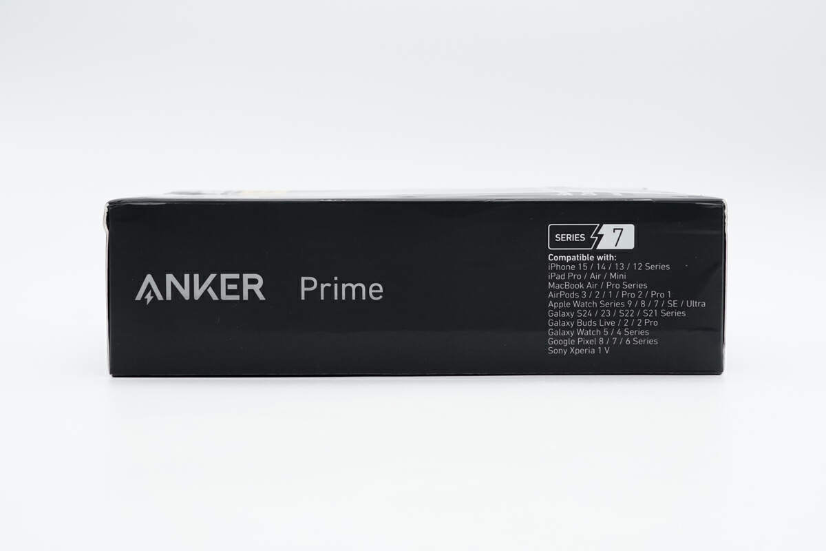
The ANKER Prime and supported devices are marked on the side.
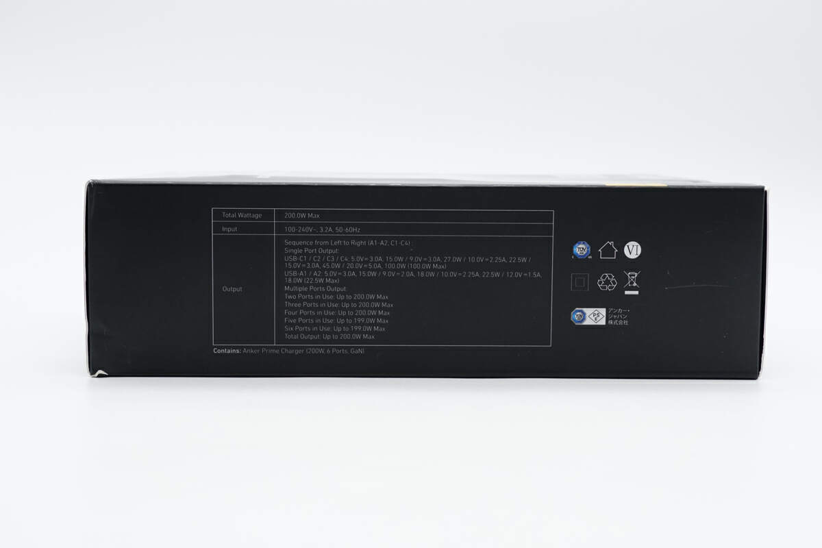
The other side has the specifications and certification information.
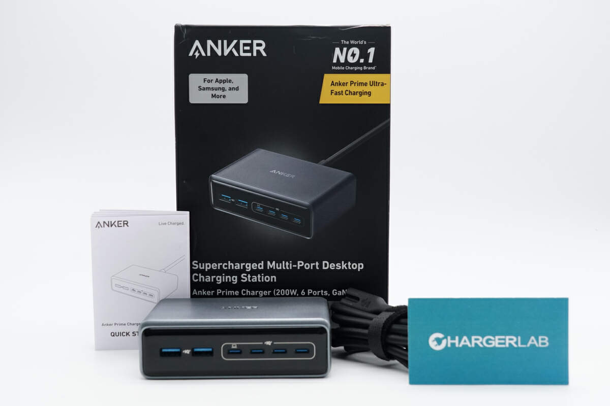
The box contains the Anker 200W GaN desktop charger, a power cord, and some documents.
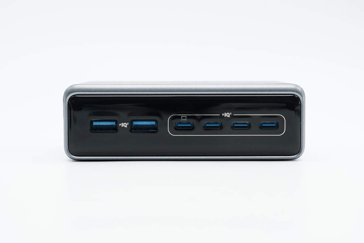
The desktop charger output panel features four USB-C ports and two USB-A ports.
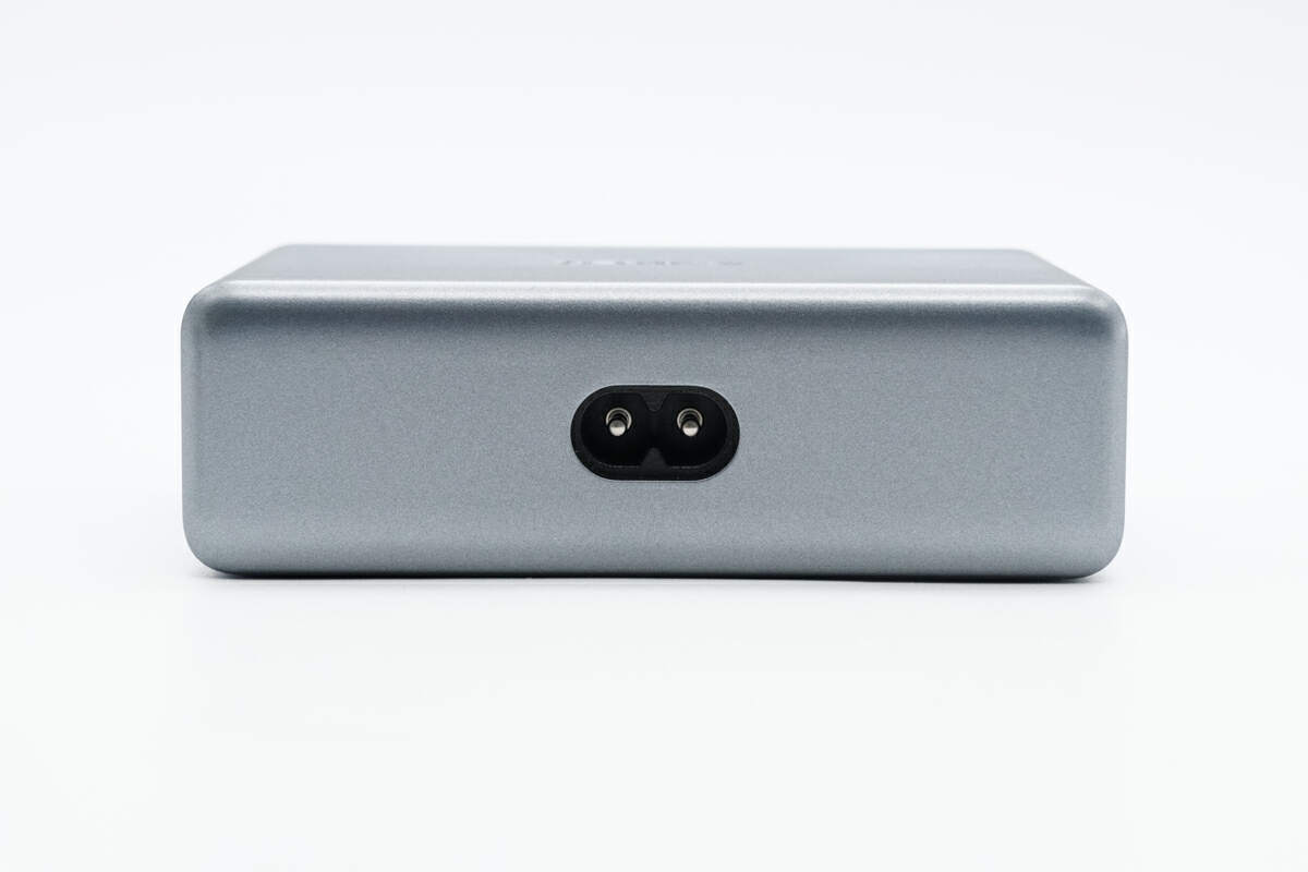
The other side has the input slot.
ANKER is printed in the middle.
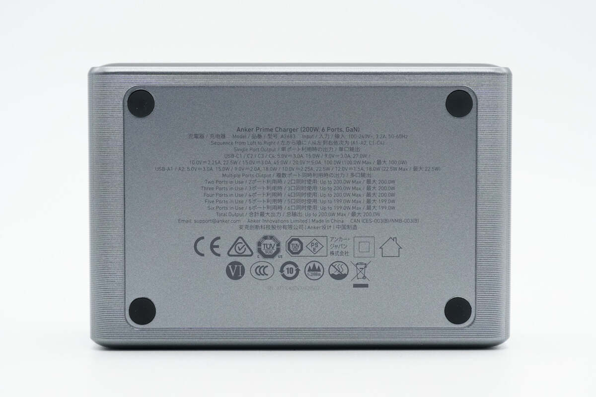
There are anti-slip pads on the bottom, and the specs info are printed on it.
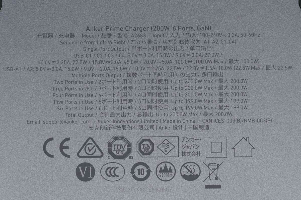
Model is A2683. It can support input of 100-240V 3.2A 50~60Hz. The power of single-port output is 5V3A, 9V3A, 10V2.25A, 15V3A, 20V5A, and the maximum is 100W.
The USB-A1/A2 support output of 5V3A, 9V2A, 10V2.25A, 12V1.5A, and the maximum is 22.5W. The maximum power when two to four ports are used simultaneously is 200W. The maximum power when five to six ports are used simultaneously is 199W. The total output is 200W.
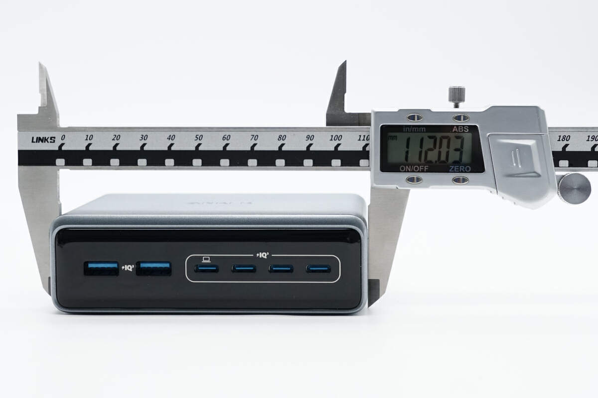
The length of the charger is about 112 mm (4.41 inches).
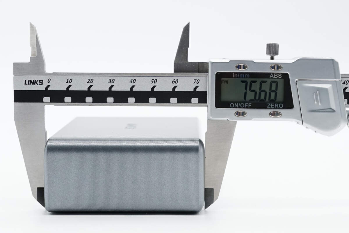
The width is about 76 mm (2.99 inches).
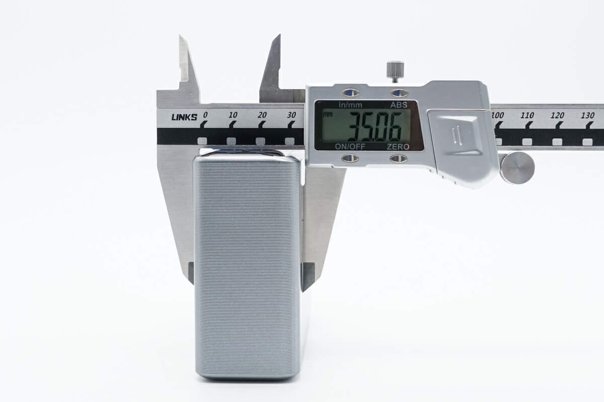
The thickness is about 35 mm (1.38 inches).
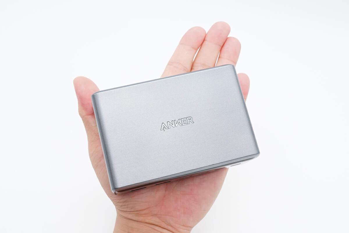
That's how big it is in the hand.
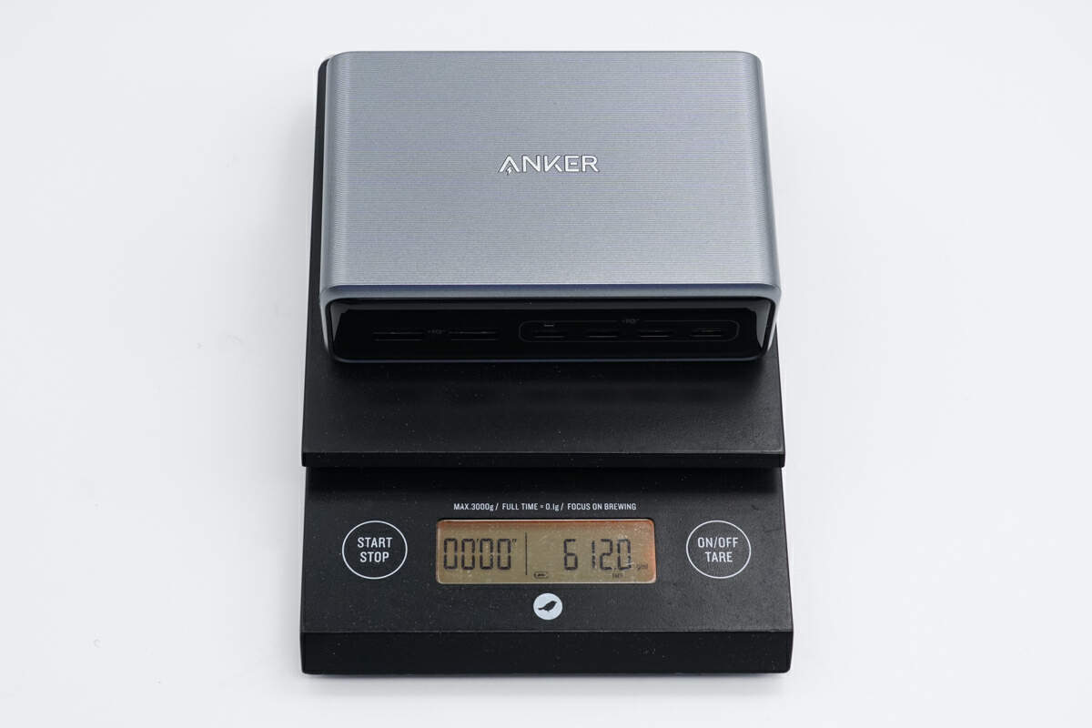
The weight is about 612 g (21.59 oz).
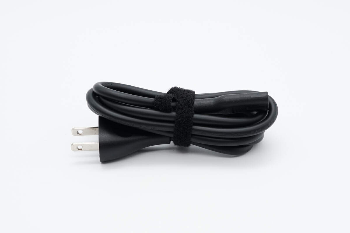
There is the power cord.
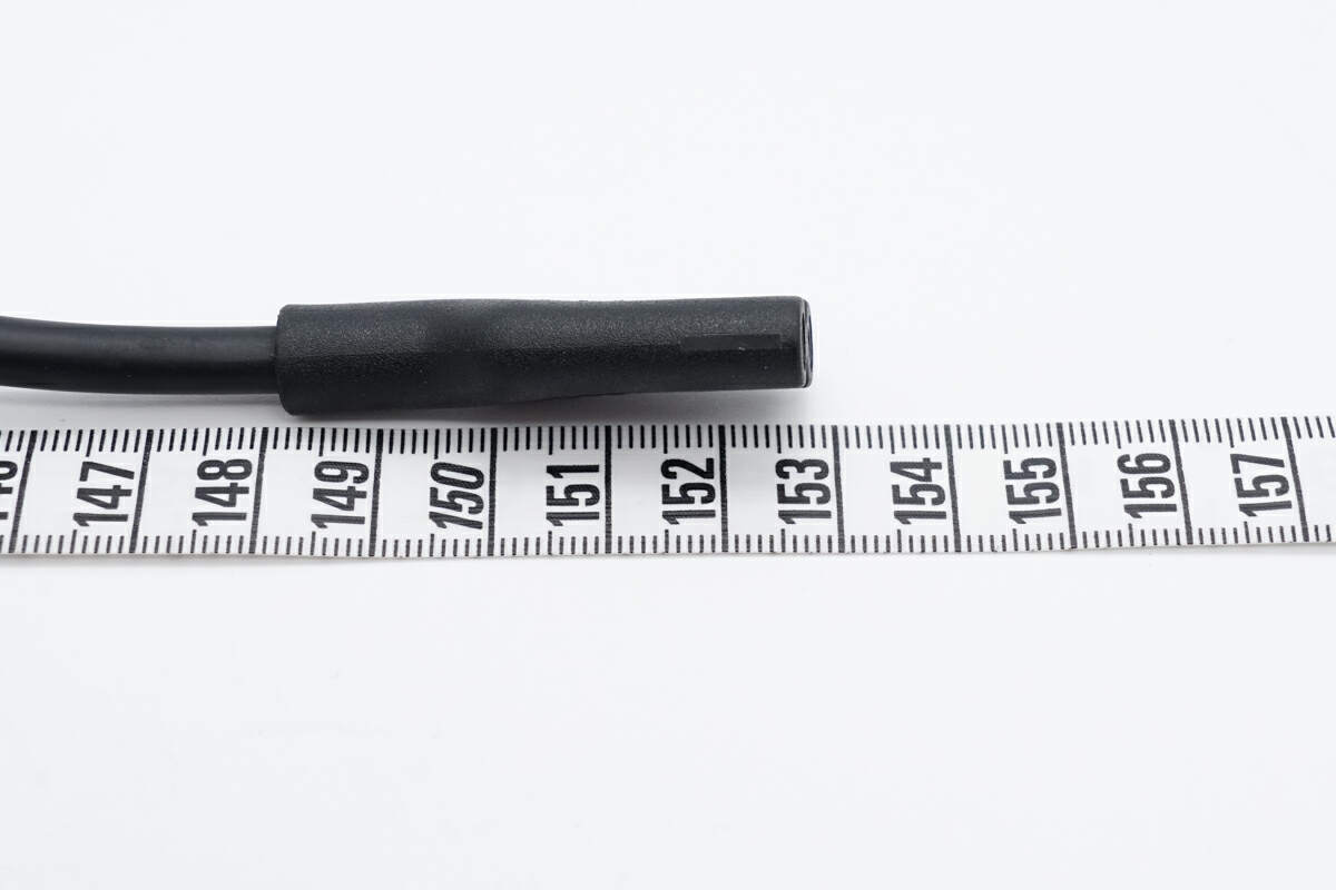
The length of the power cord is about 153 cm (60.24 inches).
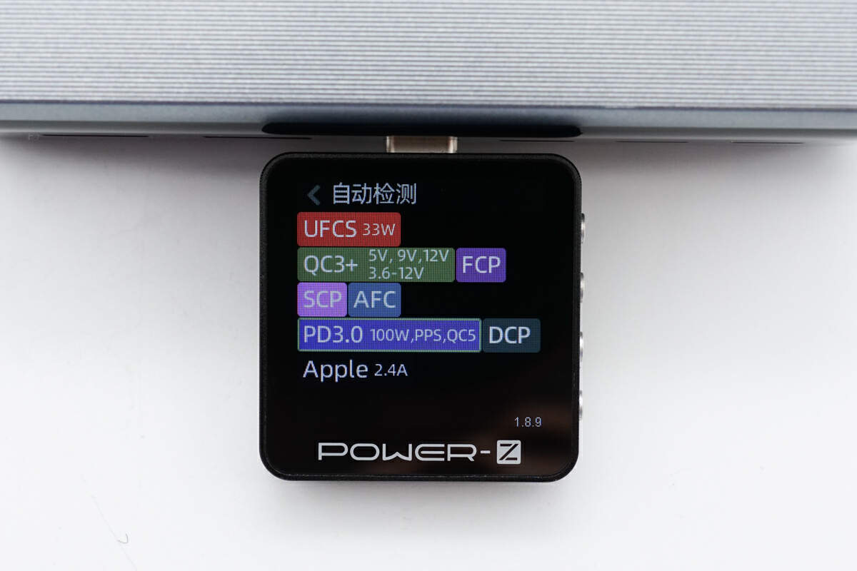
The ChargerLAB POWER-Z KM003C shows the USB-C port can support UFCS, QC3+/5, FCP, SCP, AFC, PD3.0, PPS, DCP, and Apple 2.4A charging protocols.
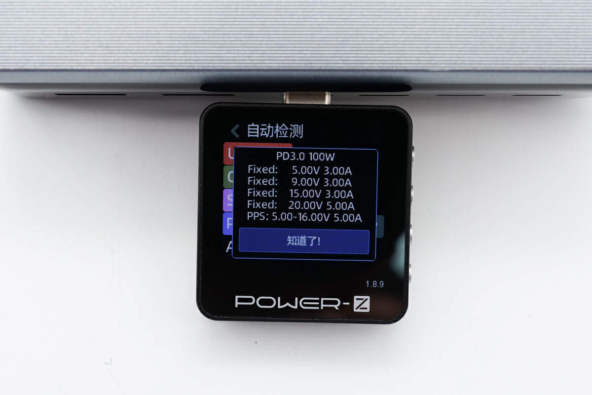
And it has four fixed PDOs of 5V3A, 9V3A, 15V3A, 20V5A, and a set of PPS, which is 5-16V5A.
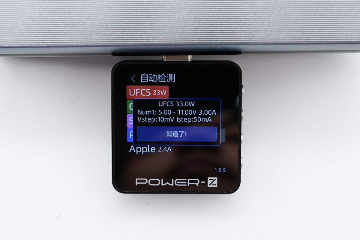
And support the 5-11V3A of UFCS.
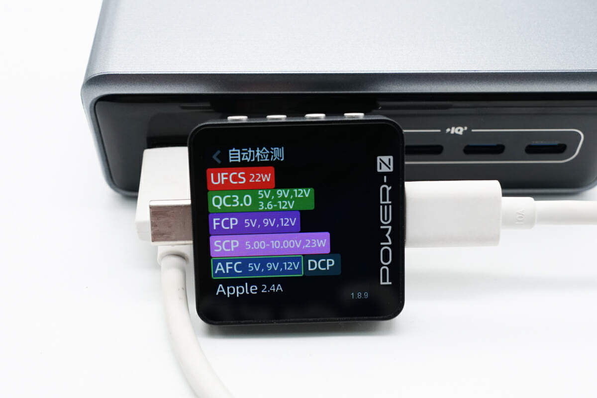
The ChargerLAB POWER-Z KM003C shows the USB-A1 port can support UFCS, QC3.0, FCP, SCP, AFC, DCP, and Apple 2.4A charging protocols.
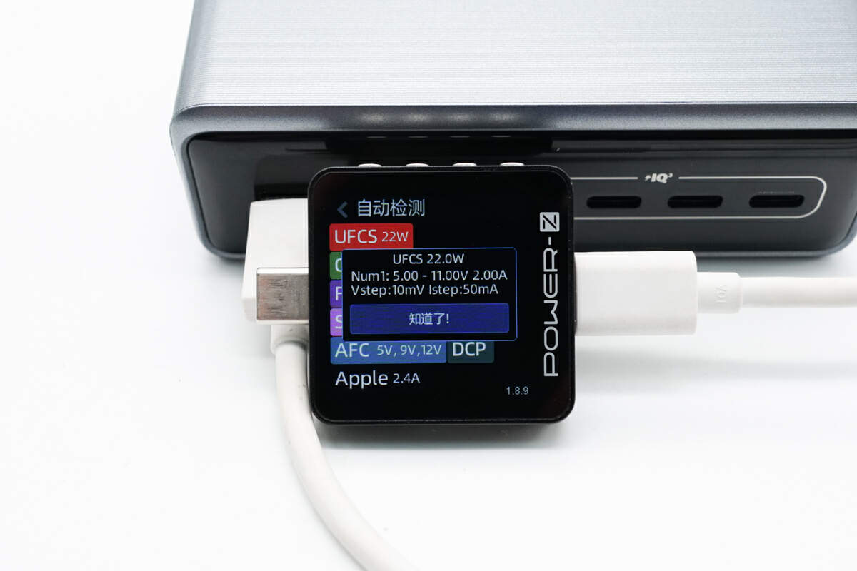
And supports the 5-11V2A of UFCS.
Teardown
Next, let's start to take it apart and take a look at the internal components.
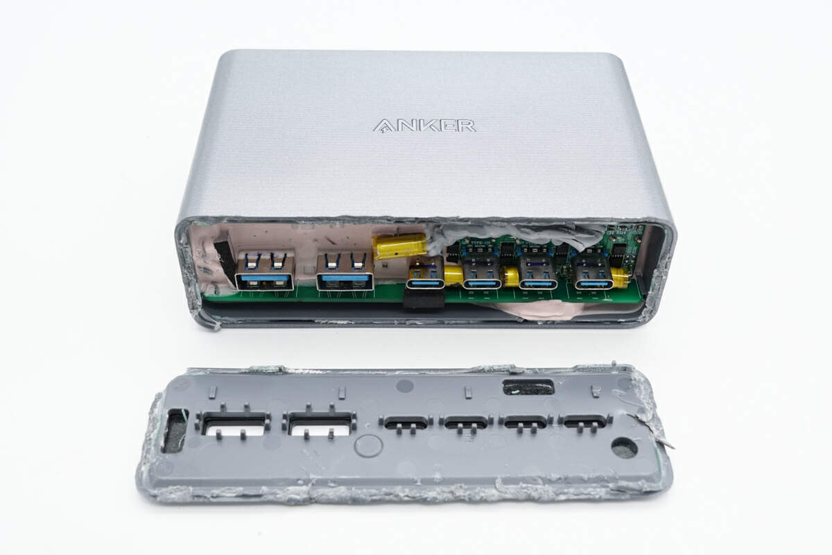
First, pry off the output panel along the gap.
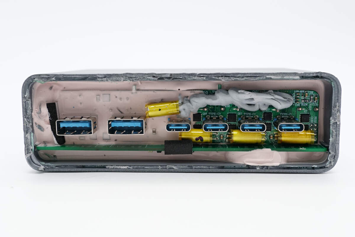
The inside of the case is filled with pink potting compound.
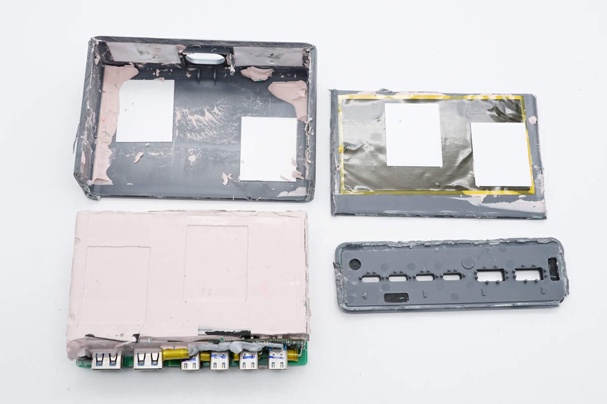
Use a cutting machine to cut open the case and take out the PCBA module.
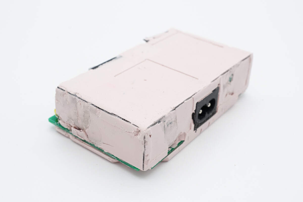
The entire PCBA module is wrapped with potting compound to improve heat dissipation.
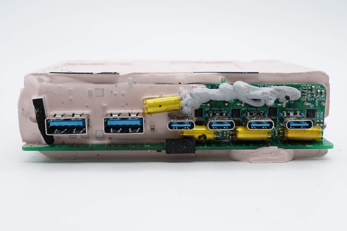
The buck PCB is soldered on the output side.
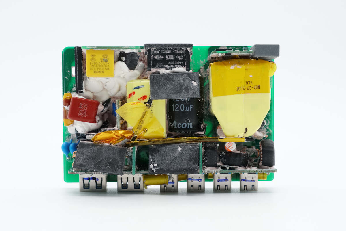
Clean up the potting compound. The input socket, filter capacitor, and buck PCB are insulated with mylar sheets, and the components are fixed with white glue.
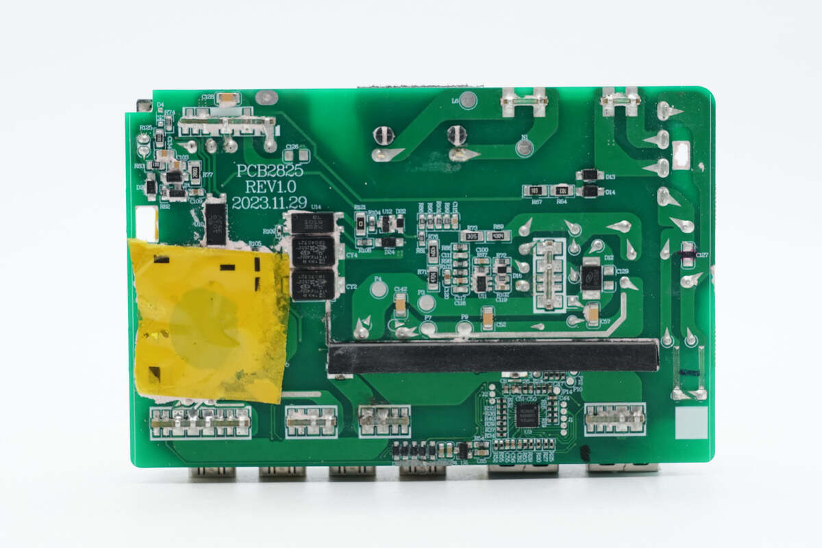
The back of the PCBA module is slotted for isolation, and a mylar sheet is inserted for insulation. The position of the synchronous rectifier is coated with thermal conductive glue to enhance heat dissipation.
ChargerLAB found it adopts a PFC+AHB architecture and five synchronous buck circuits.
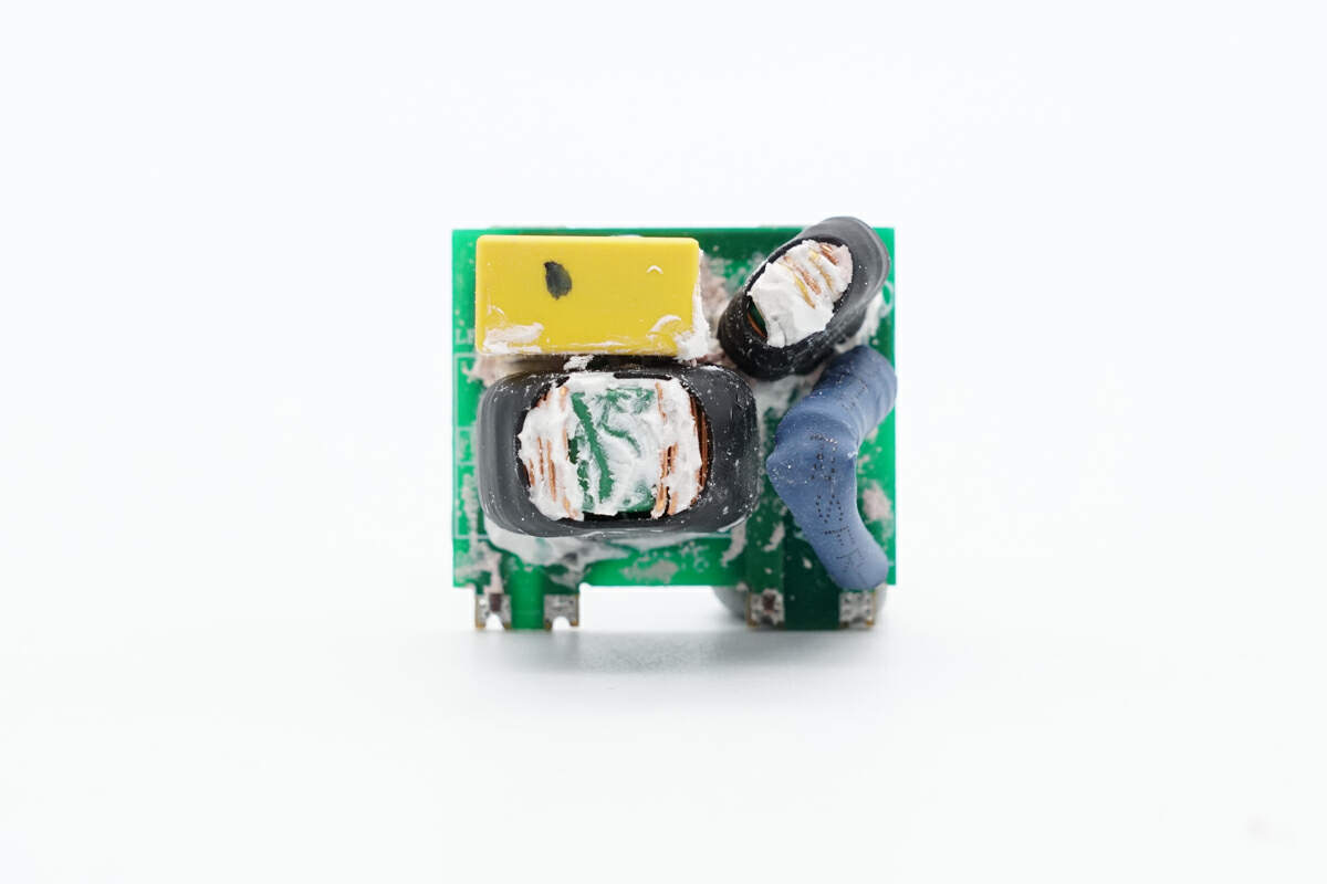
The yellow safety X2 capacitor, common mode choke, and fuse are soldered on the front of the input filter PCB.
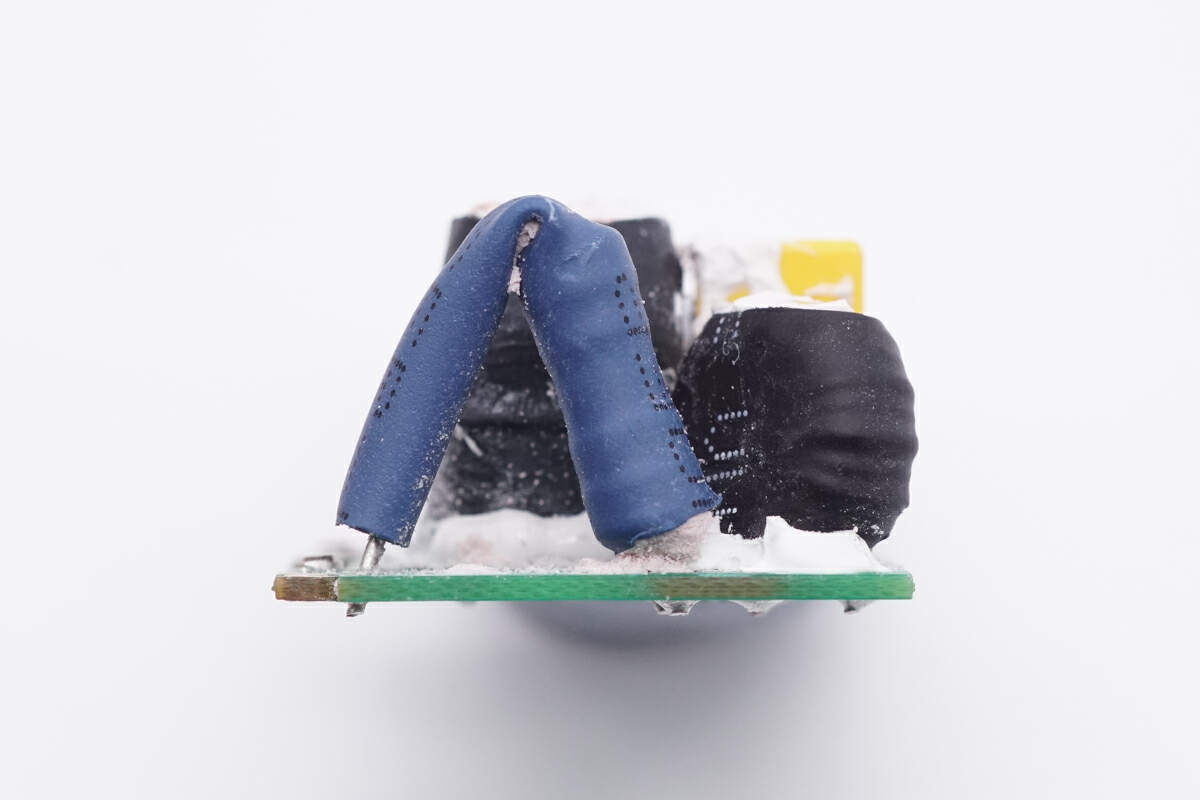
The fuse is insulated by heat-shrinkable tubing.
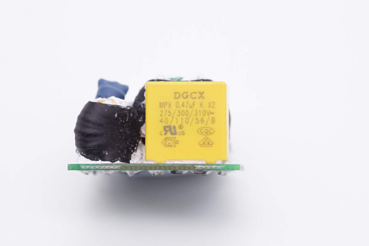
The yellow safety X2 capacitor is from DGCX. 0.47μF.
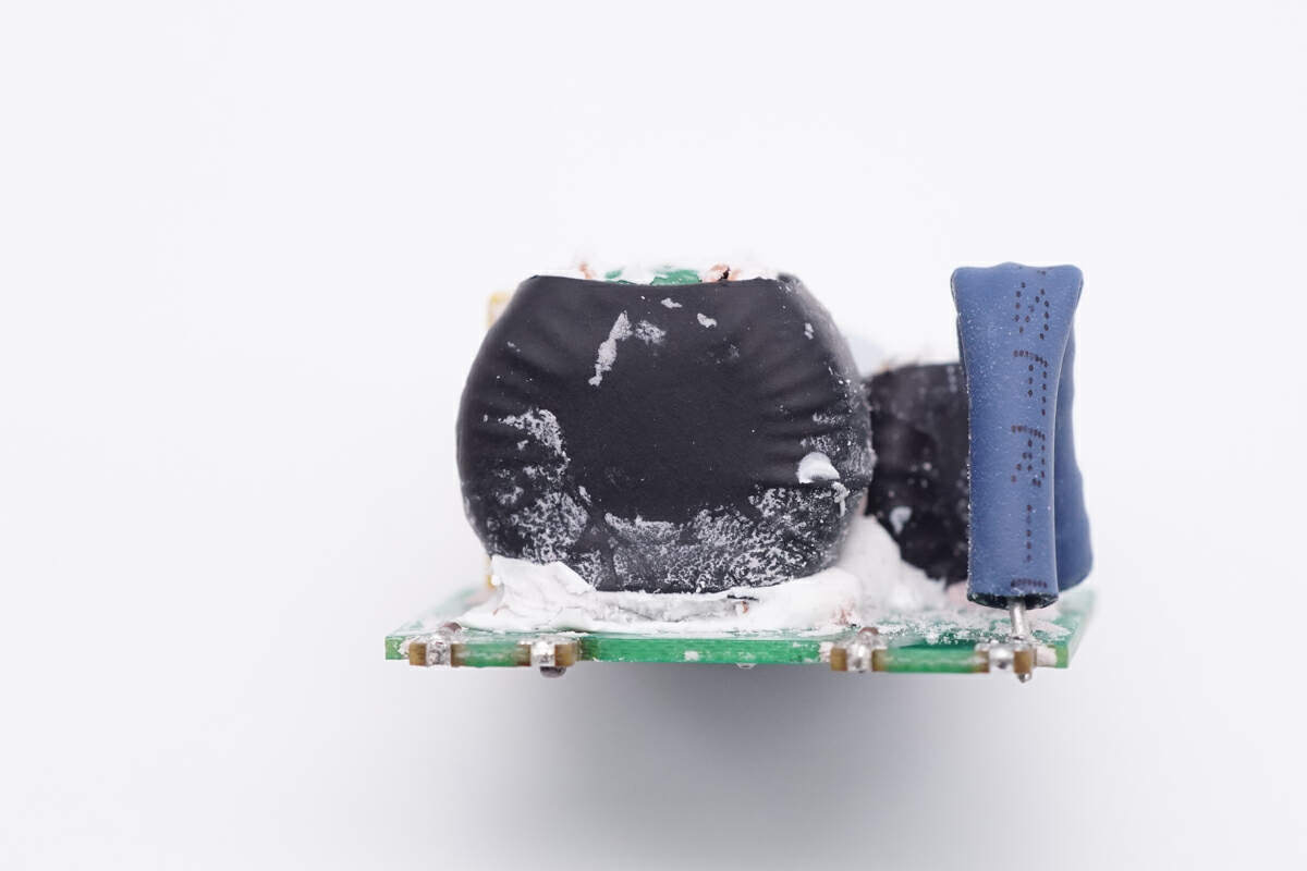
Both common mode chokes are insulated by heat-shrinkable tubing.
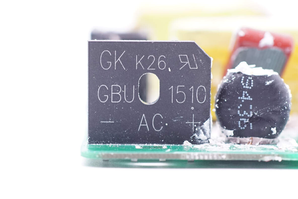
The bridge rectifier soldered on the side of the PCBA module is from GK. It adopts GBU package. 1000V 15A. Model is GBU1510.
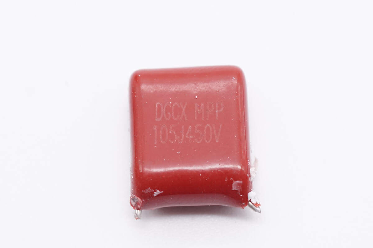
The film capacitor is from DGCX. 1μF 450V.
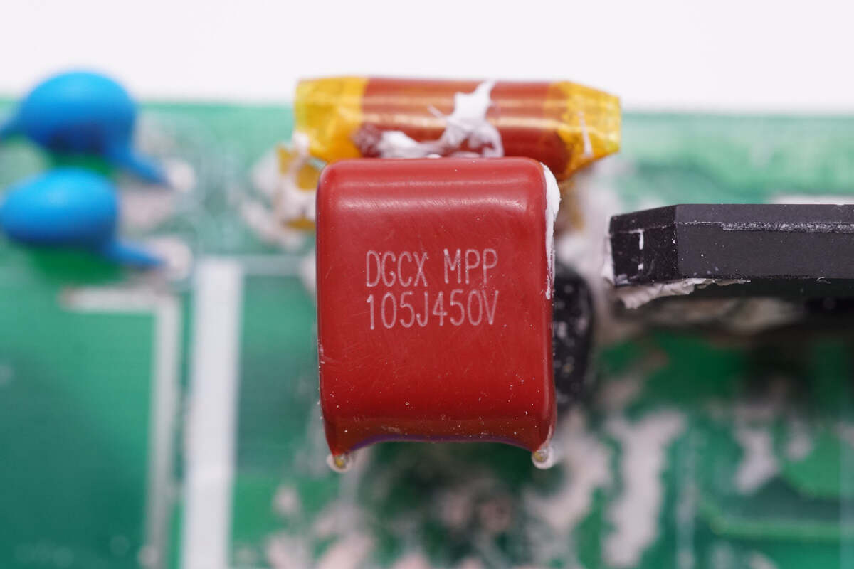
The other film capacitor has the same specifications.
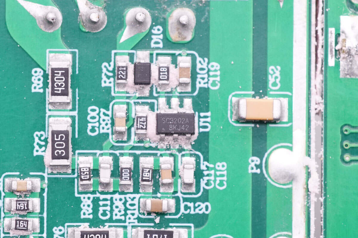
The PFC controller is from SouthChip and adopts SOT23-6 package. It is a high-efficiency boost PFC controller. Model is SC3202.
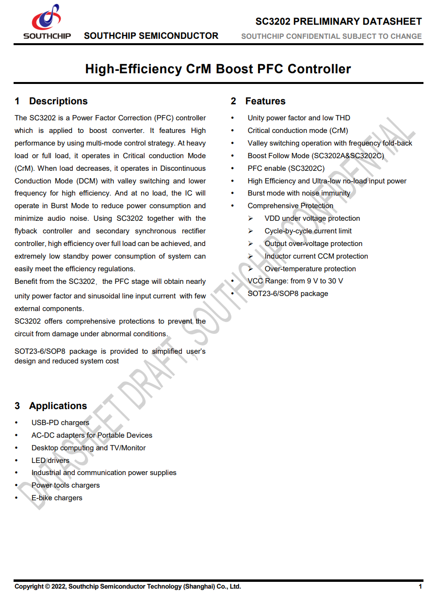
Here is all the information about the SouthChip SC3202.
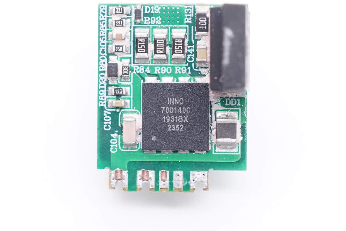
PFC MOSFET and rectifier are soldered on the separate PCB. The PFC MOSFET is from Innoscience and adopts DFN8*8 package. 700V 140mΩ. Model is INN700D140C.
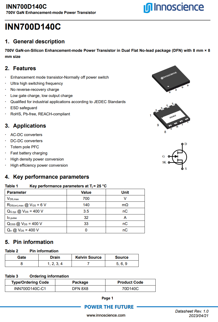
Here is all the information about the Innoscience INN700D140C.
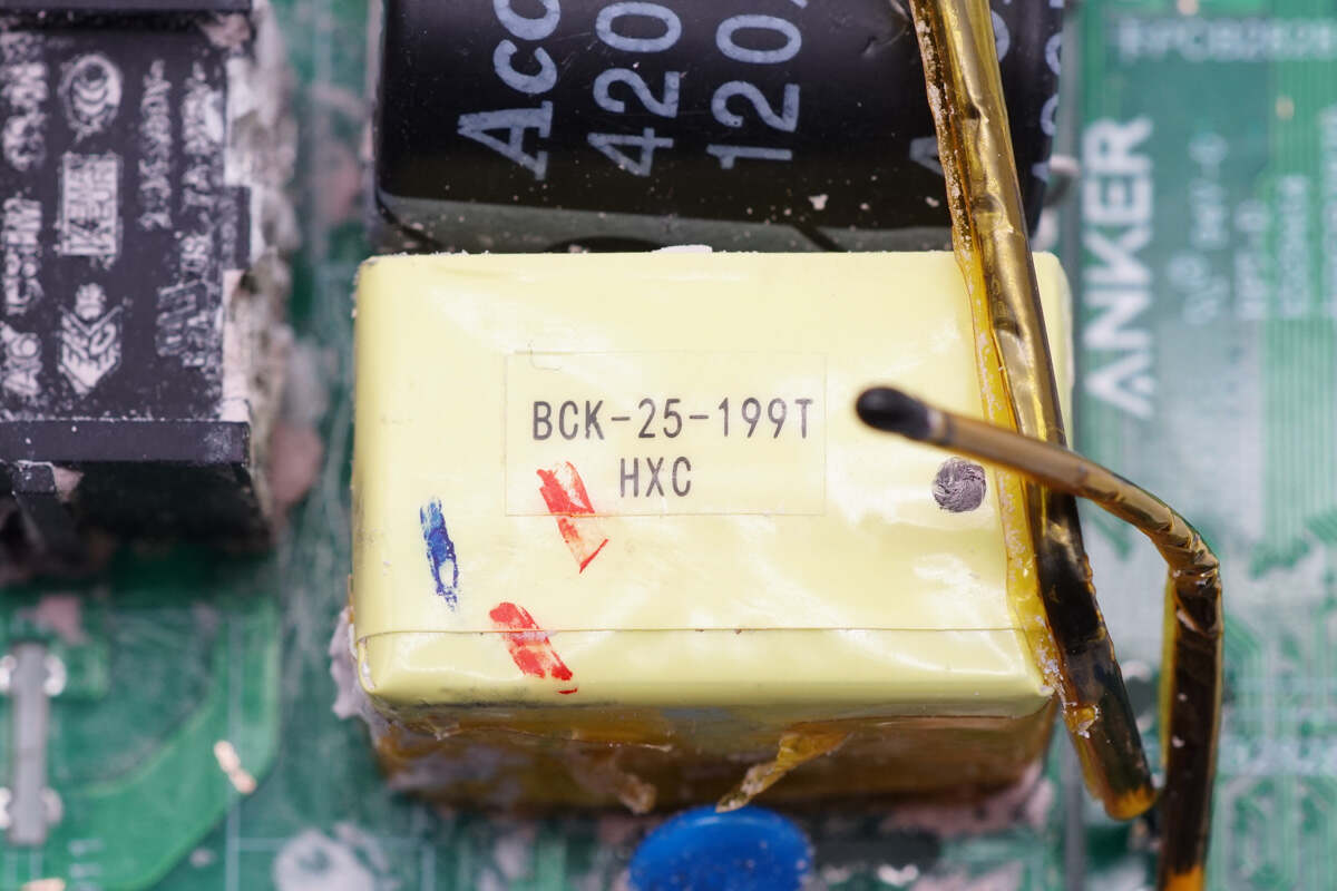
The PFC boost inductor is insulated by tape, and a thermistor is attached to detect the temperature.
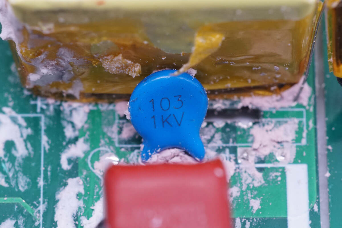
There is a capacitor near the PFC boost inductor. 0.01μF 1KV.
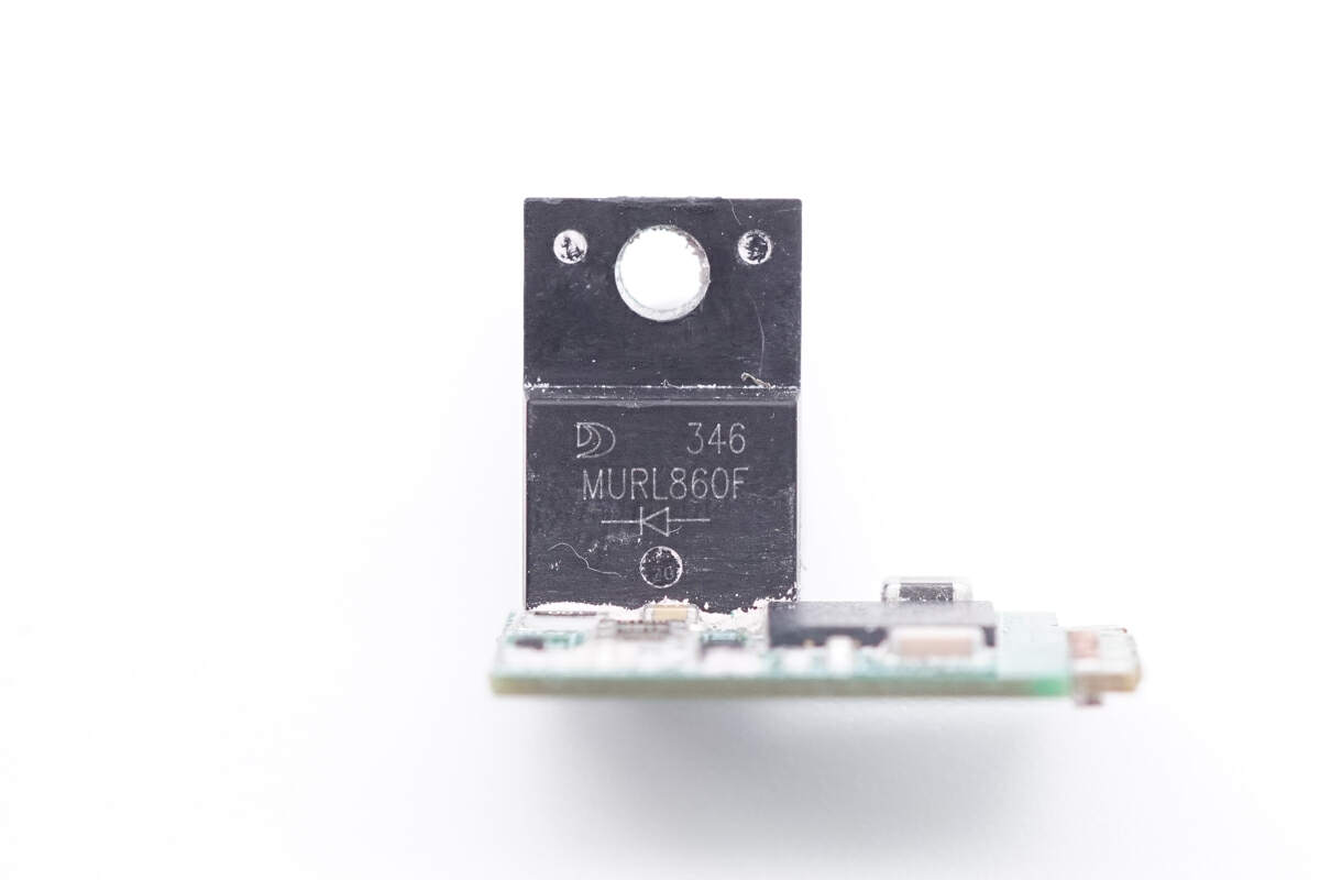
The PFC rectifier is from JINGDAO and adopts ITO-220ACW package. 600V 8A. Model is MURL860F.
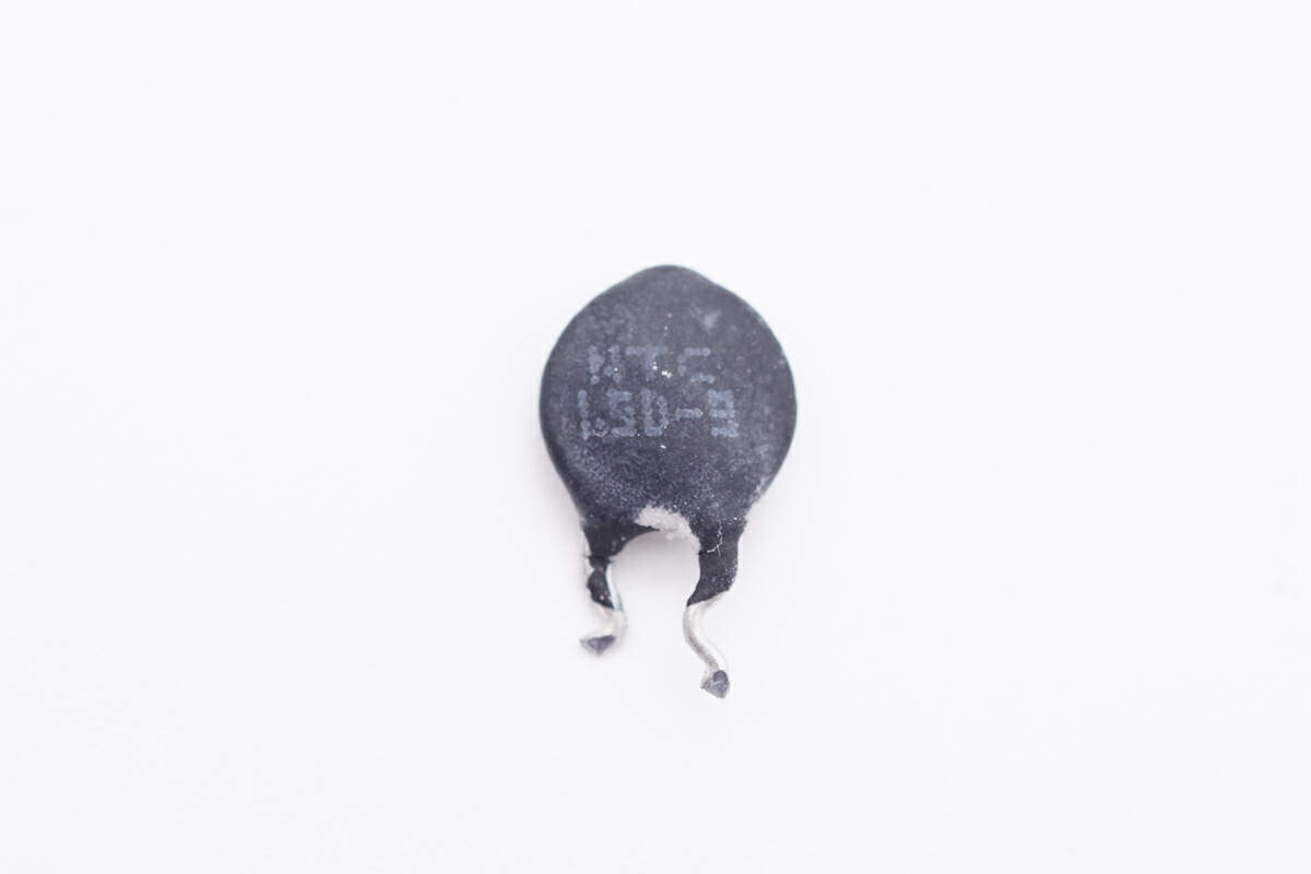
The NTC thermistor is used to suppress the inrush current when charging the high-voltage capacitor.
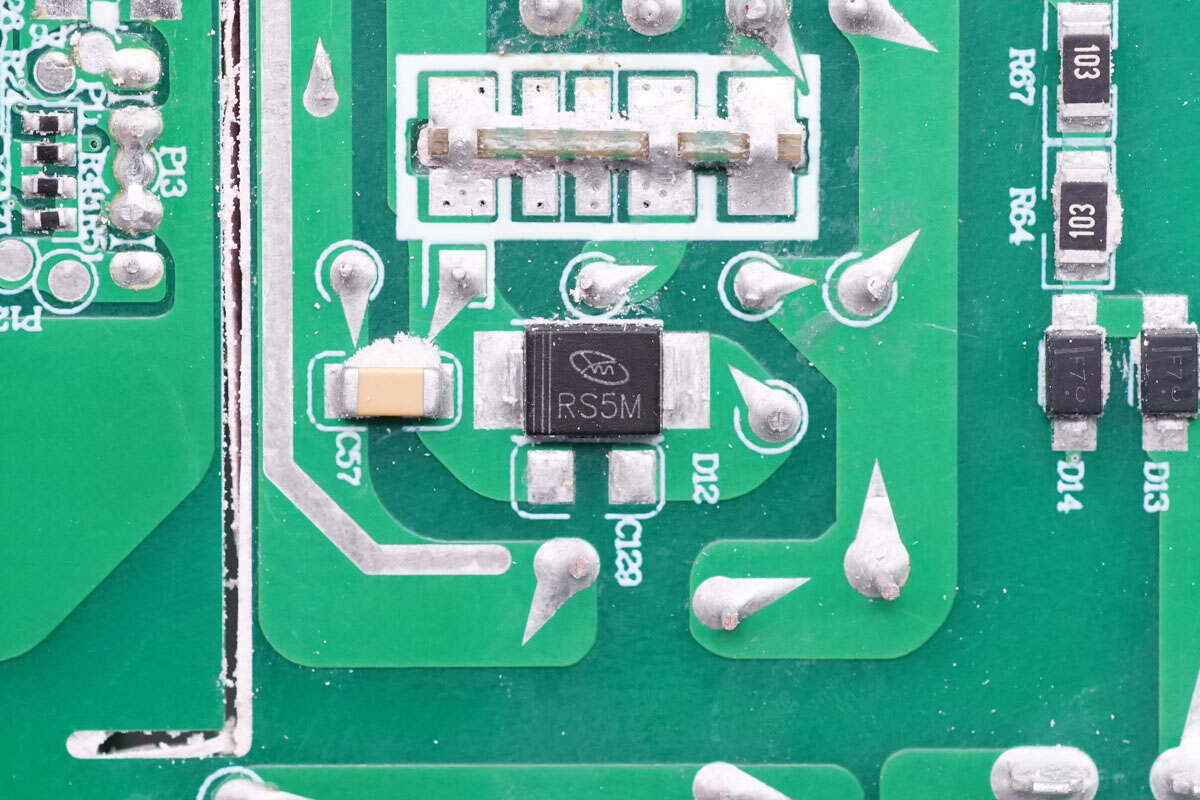
The diode marked with RS5M is used for PFC bypass.
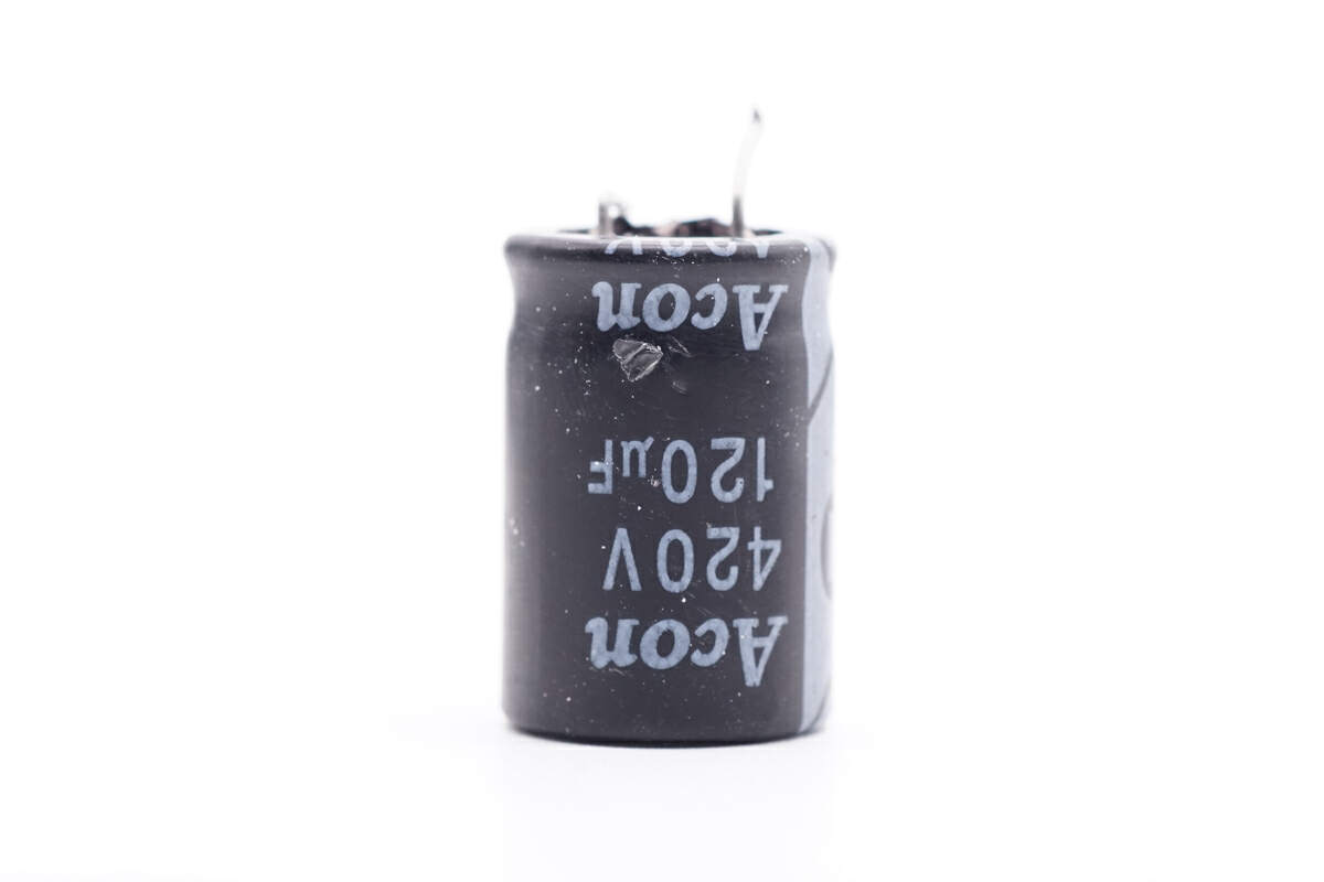
The filter capacitor is from Acon. 420V 120μF.
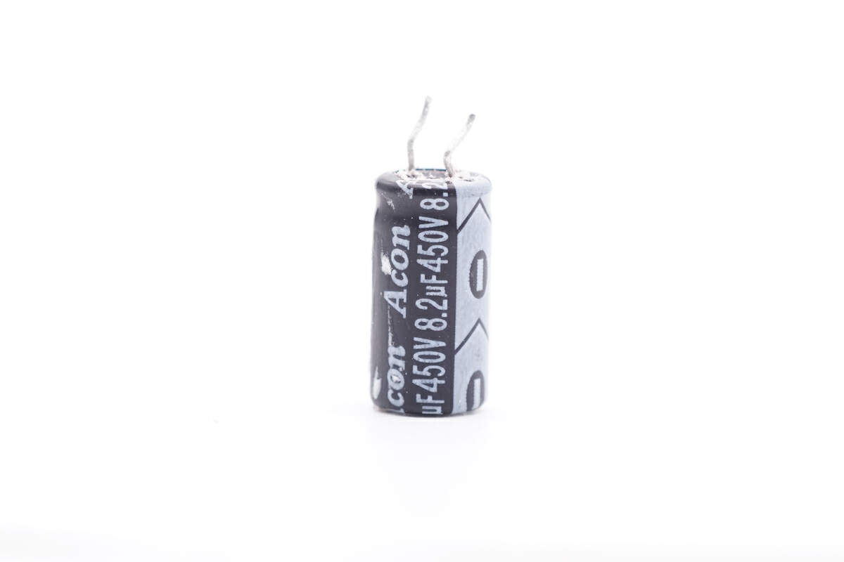
This is another filter capacitor. 8.2μF 450V.
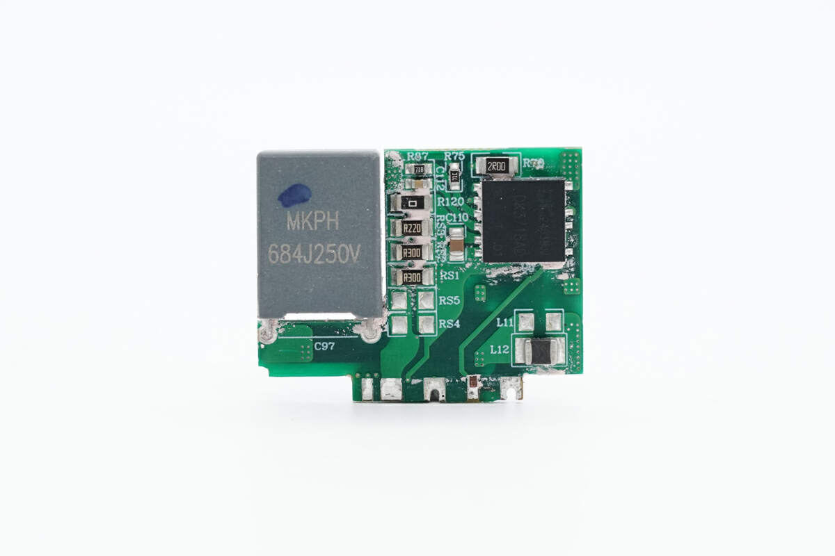
The resonant capacitor and AHB GaN IC are soldered on a small vertical PCB.
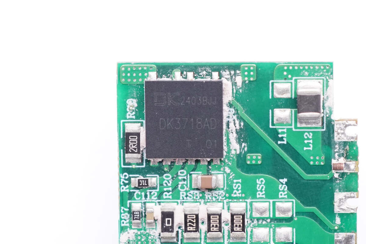
The AHB GaN IC is from DONGKE and adopts DFN8*8 package. It adopts an asymmetric half-bridge architecture, integrates two GaN power components in the AC-DC power switch chip, and has complete protection functions. It can be used with a variety of charging devices. Model is DK3718AD.
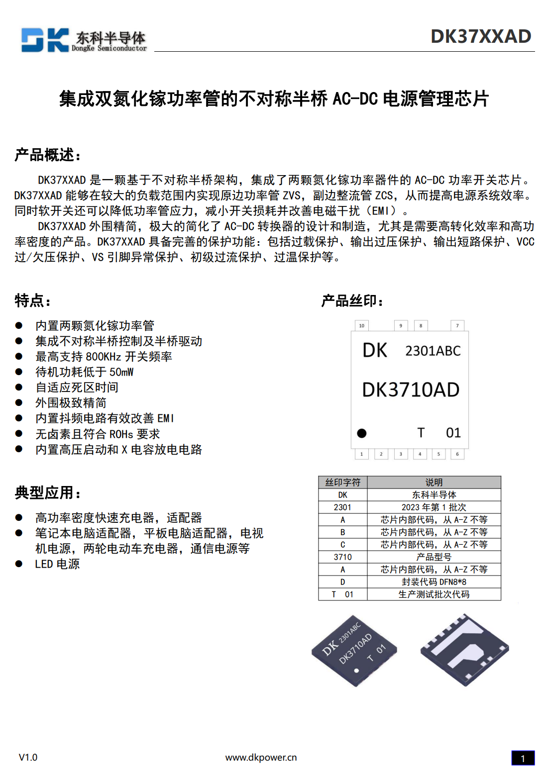
Here is all the information about the DONGKE DK3718AD.
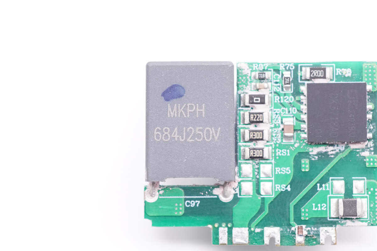
Here is the resonant capacitor. 0.68μF 250V.
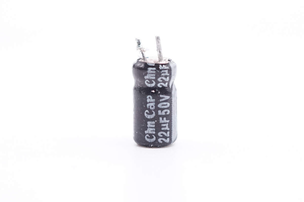
The filter capacitor that powers the master control chip is from CanCap. 22μF 50V.
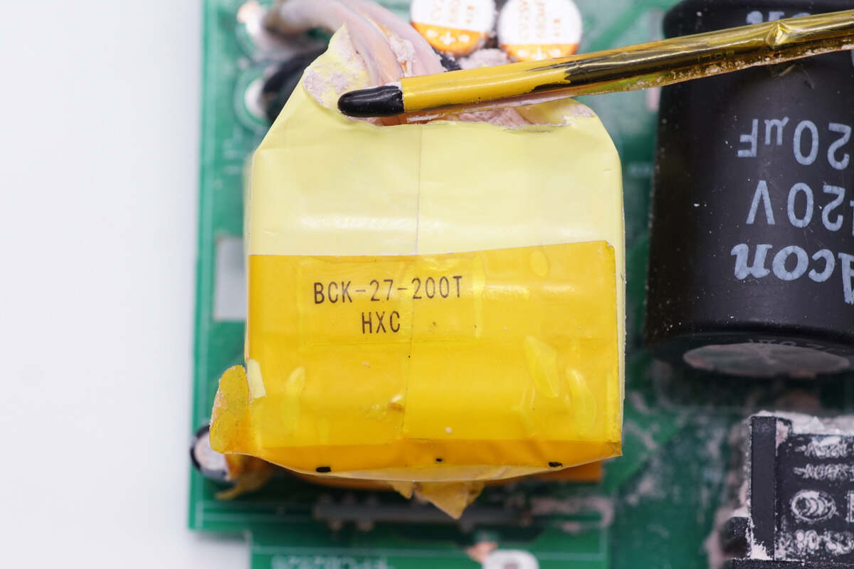
The magnetic core of the transformer is insulated by tape and equipped with a thermistor to detect the temperature.
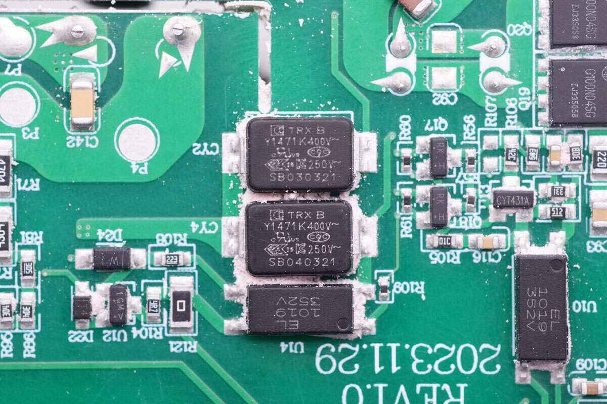
The SMD Y capacitors are from TRX.
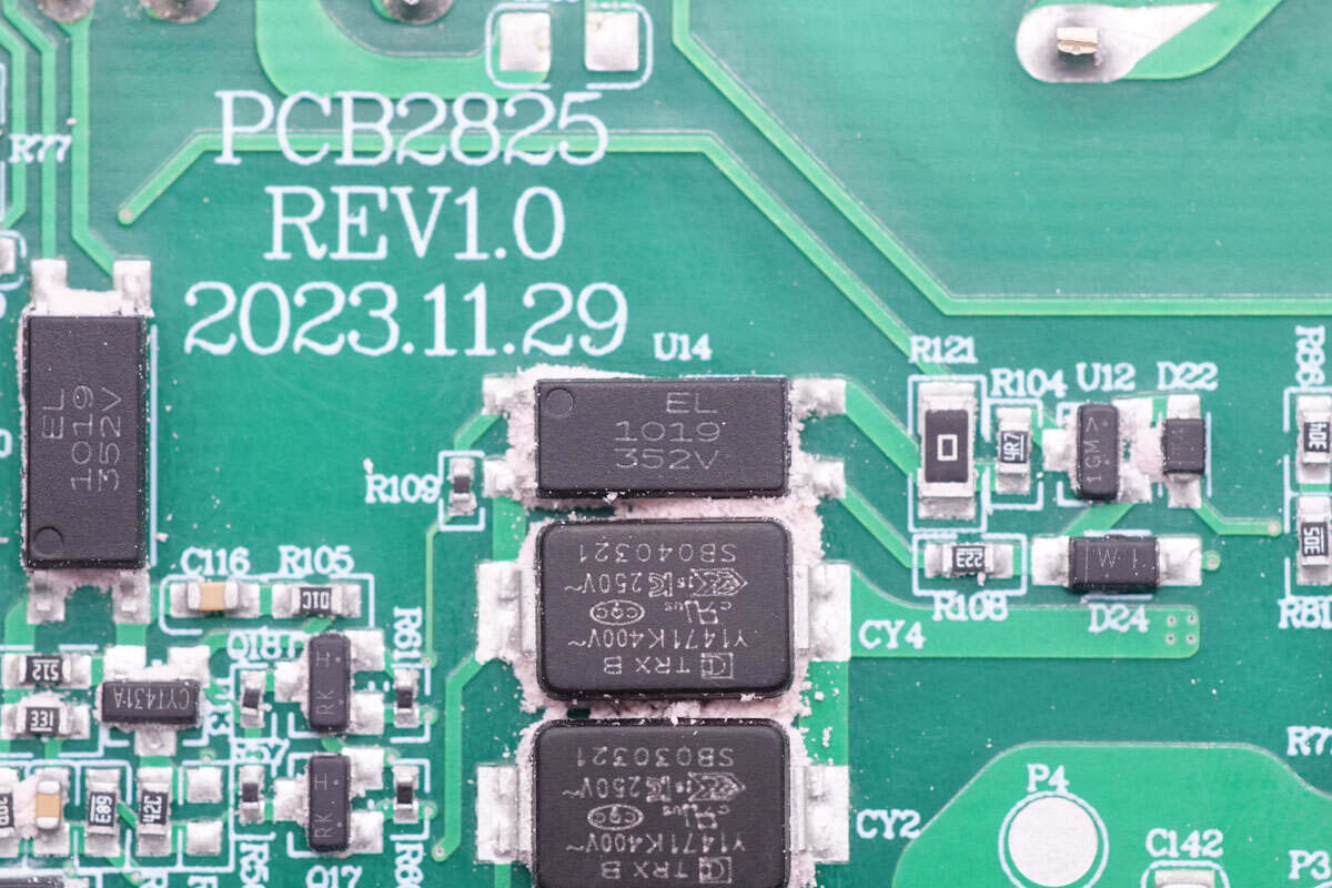
The optocoupler used for PFC switch control is from Everlight. Model is EL1019.
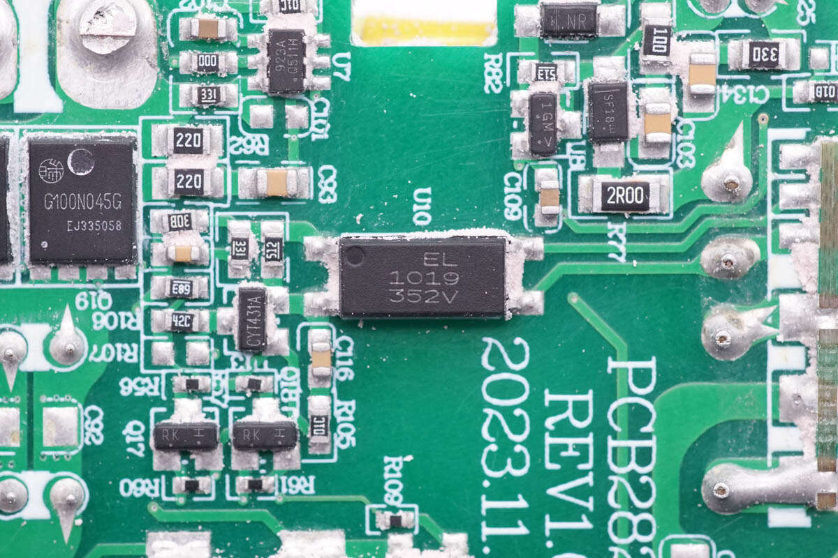
Another optocoupler is used for output voltage feedback. Model is EL1019.
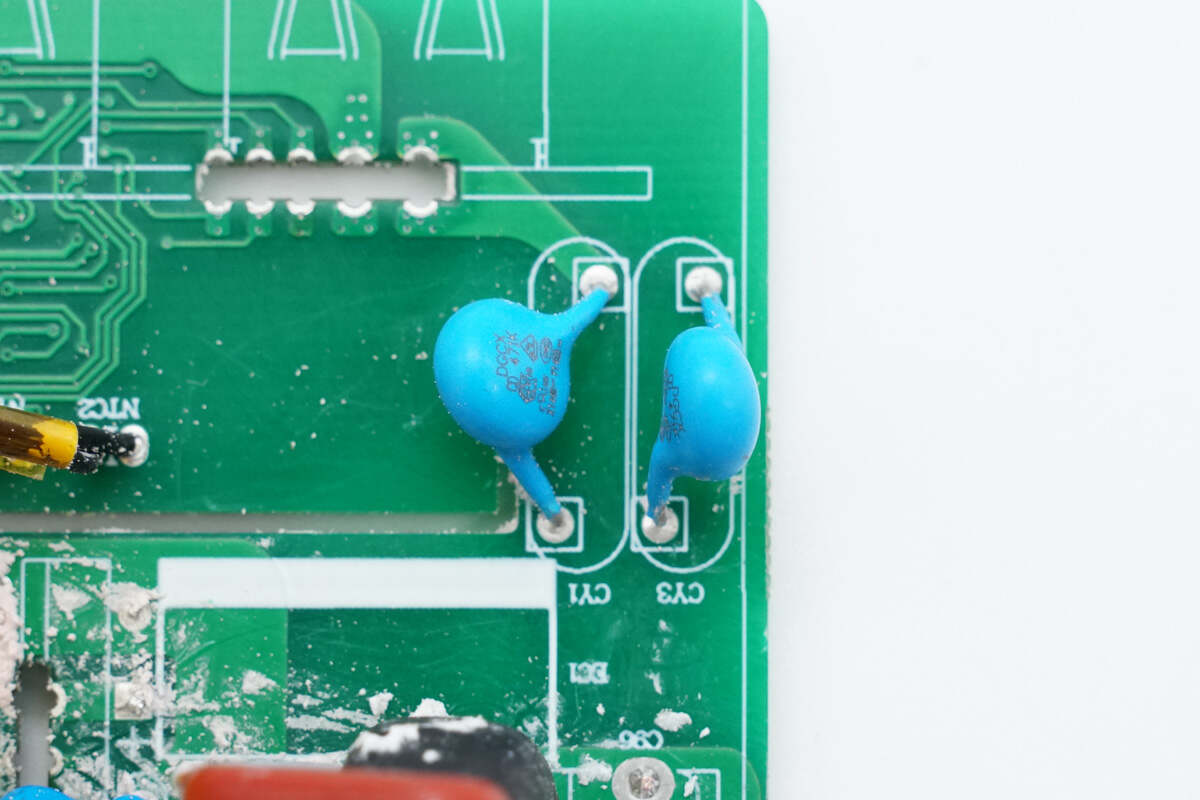
The two plug-in blue Y capacitors are from DGCX.
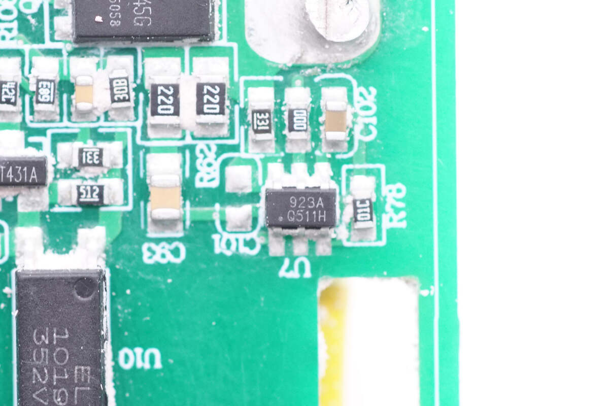
The digital synchronous rectifier controller is from HYASiC and adopts SOT23-6 package. Its high current driving capability is suitable for a variety of synchronous rectifiers. Model is HY923.
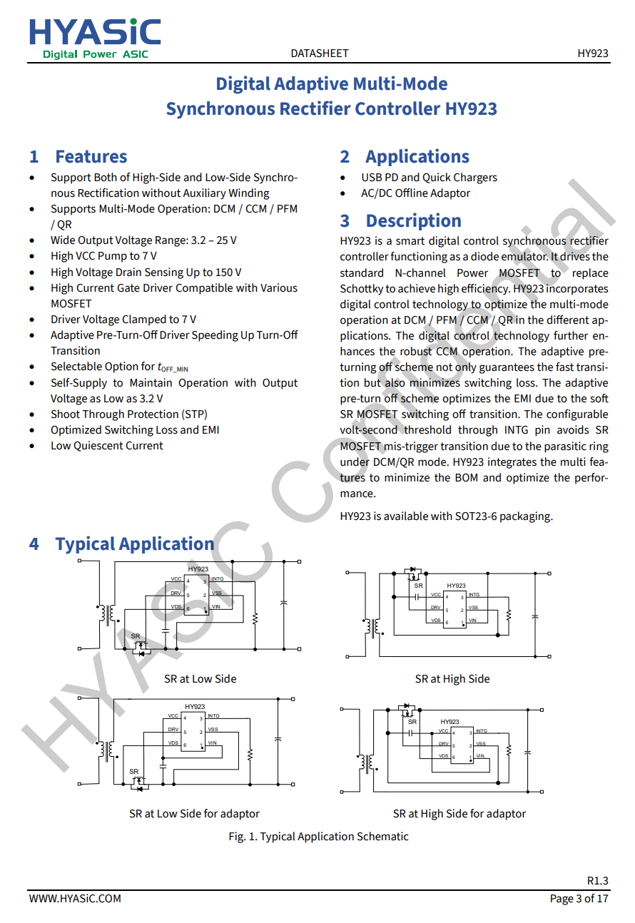
Here is all the information about the HYASiC HY923.
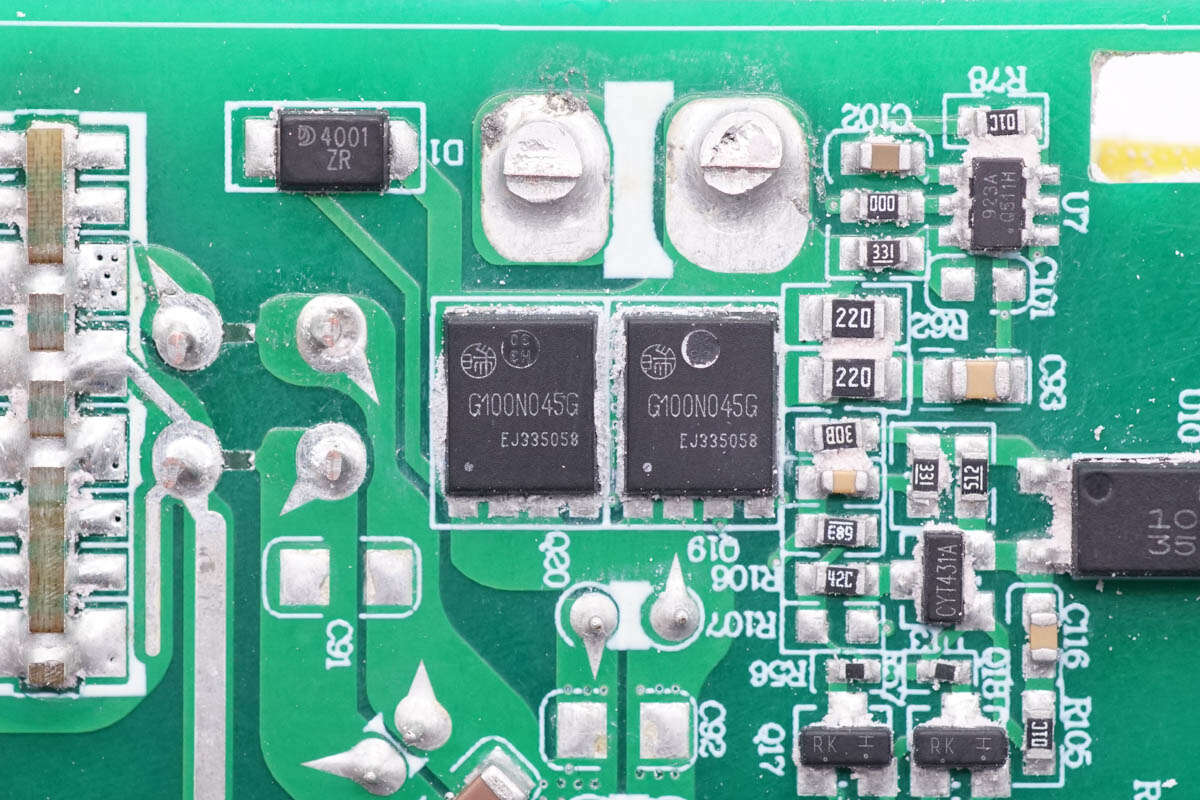
The synchronous rectifiers are from HRmicro and adopt PDFN5*6 package. Two were used in parallel. 100V 4.2mΩ. Model is HRG100N045G.
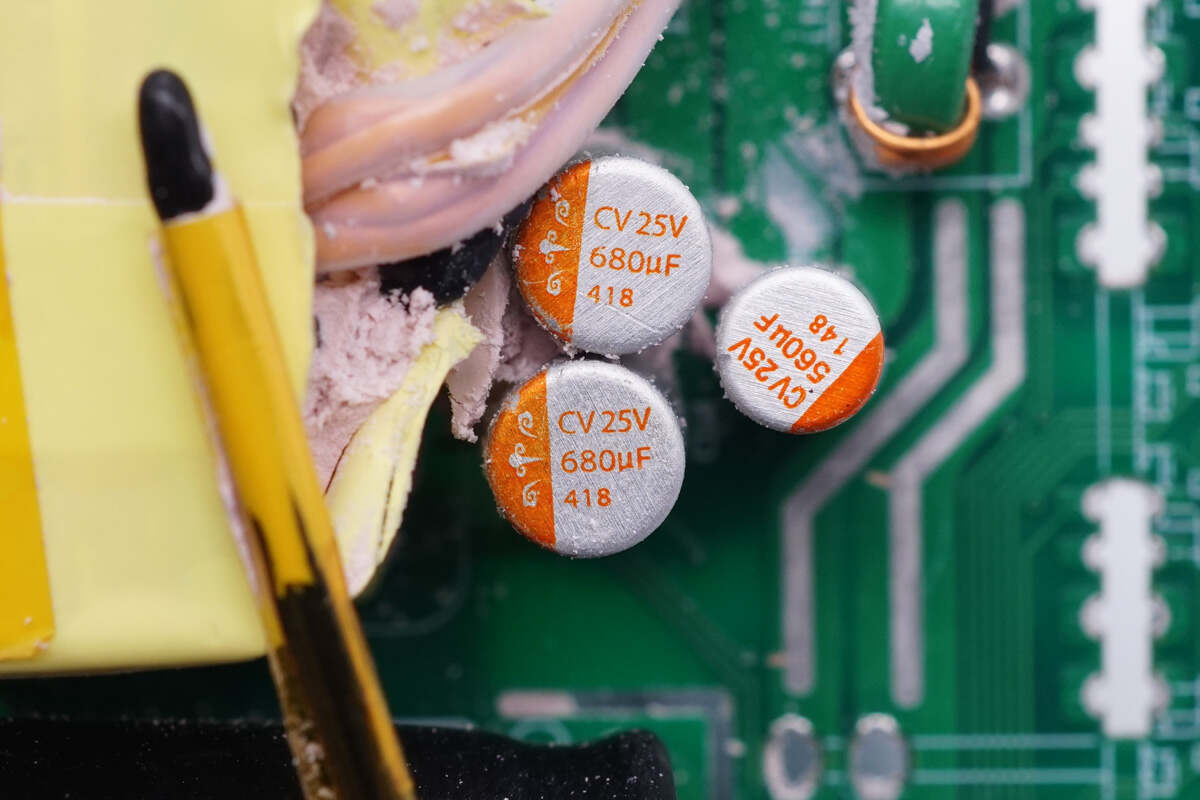
The solid capacitors for output filtering are from CanCap. Two of them are 25V 680μF.
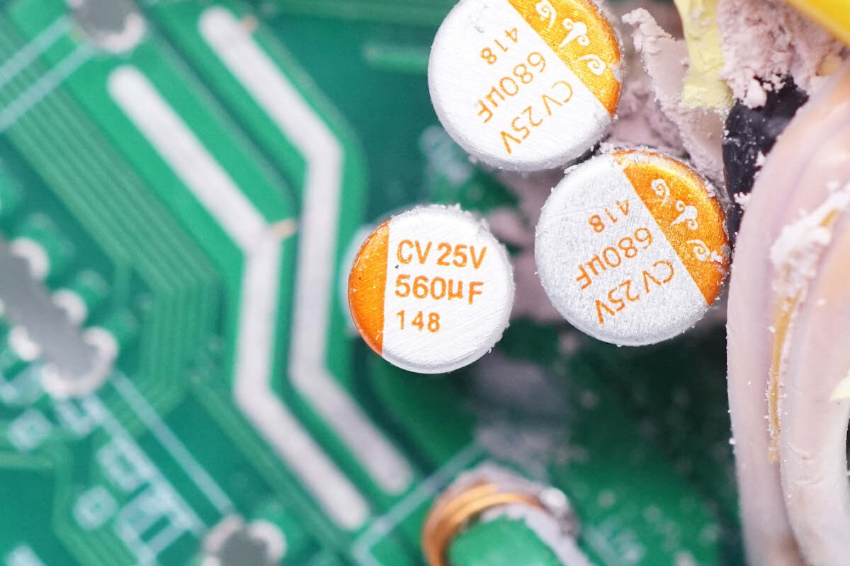
One of them is 25V 560μF.
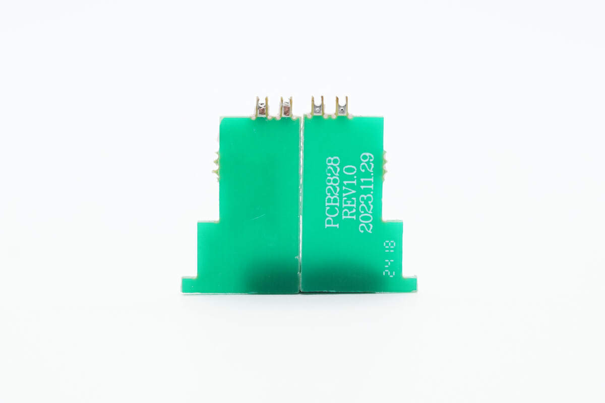
The two PCBs used to support the output buck PCB are fixed by soldering.
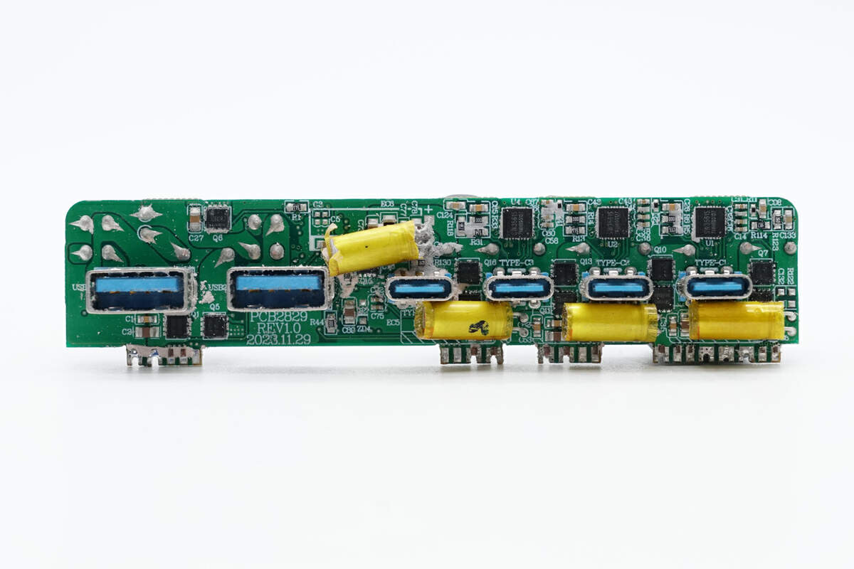
The front of the output buck PCB is equipped with USB ports, filter capacitors, synchronous buck MOSFETs, and buck protocol chips.
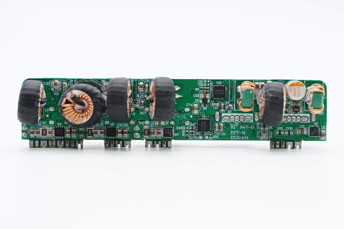
There are five buck inductors, two buck protocol chips, the VBUS MOSFETs, and current detection resistors corresponding to the USB-C ports and the filter capacitors and filter inductor of the USB-As port on the back of the output buck PCB.
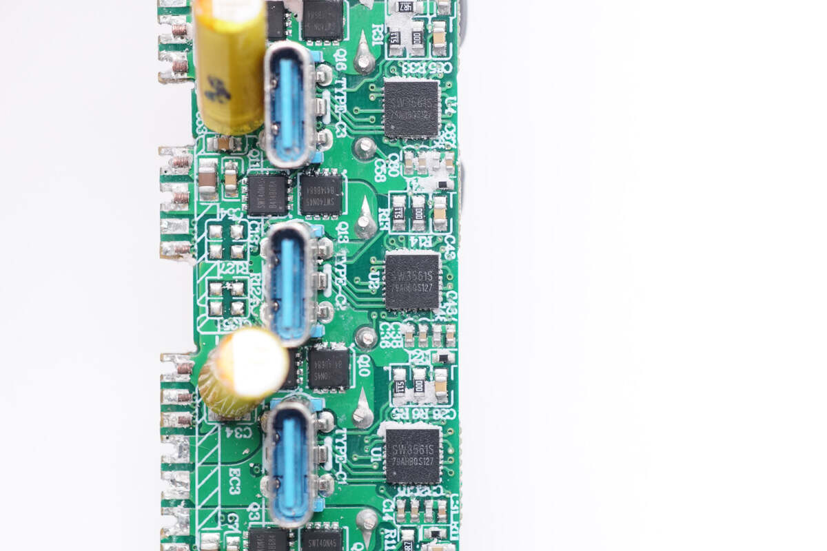
All five buck protocol chips are from iSmartWare and adopt QFN32 package. It integrates the high-efficiency synchronous buck controller and complete protection functions. Model is SW3561.
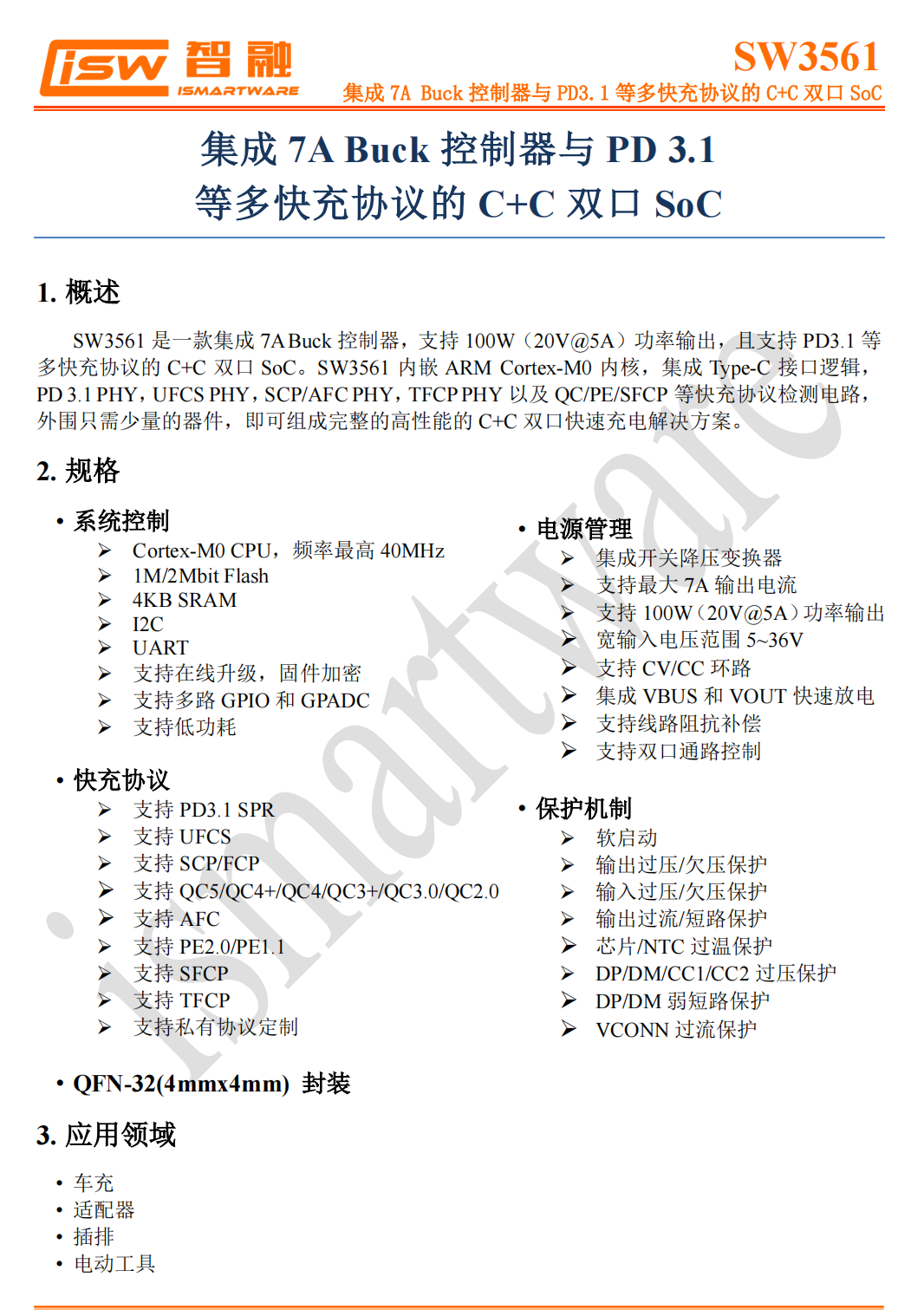
Here is all the information about the iSmartWare SW3561.
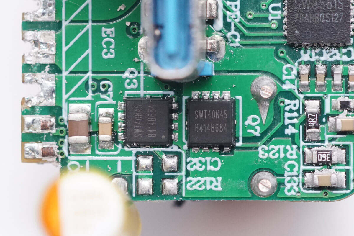
The MOSGETs marked with SWT40N45 are from iSmartWare.
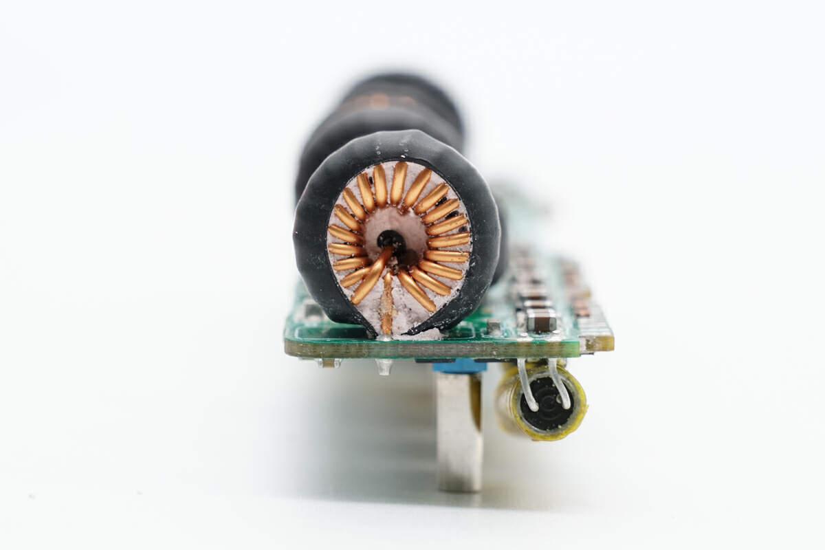
The buck inductor is wounded with magnetic ring and insulated by heat-shrinkable tubing.
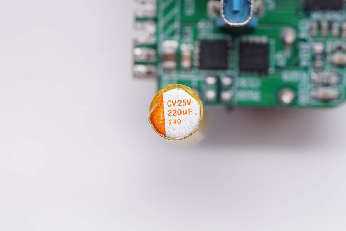
The solid capacitor for output filtering is from CanCap. 25V 220μF.
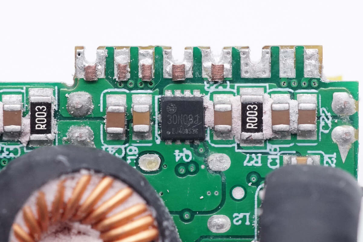
The VBUS MOSFET is from HRmicro and adopts DFN3*3-8L package. Model is HRT30N08J. 30V 5.5mΩ.
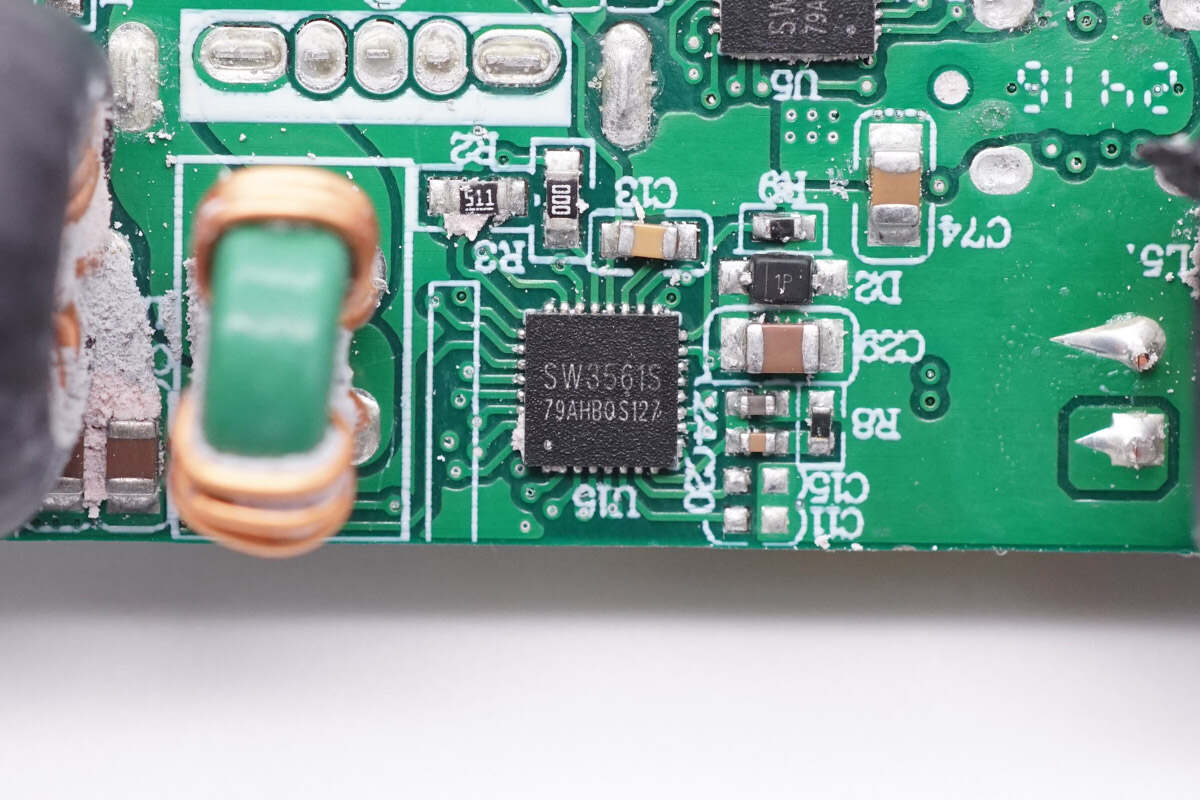
The buck protocol chip for the USB-A port is also from iSmartWare. Model is SW3561.
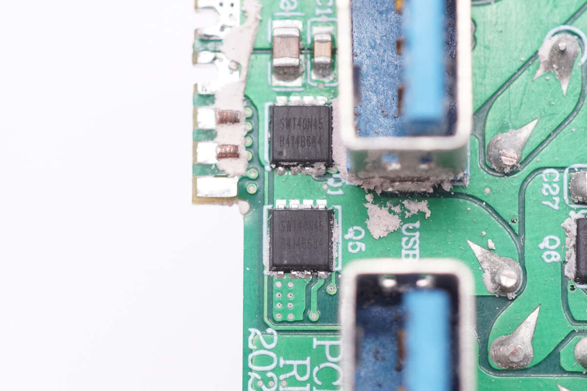
These two synchronous buck MOSFETs are from iSmartWare. Model is SWT40N45.
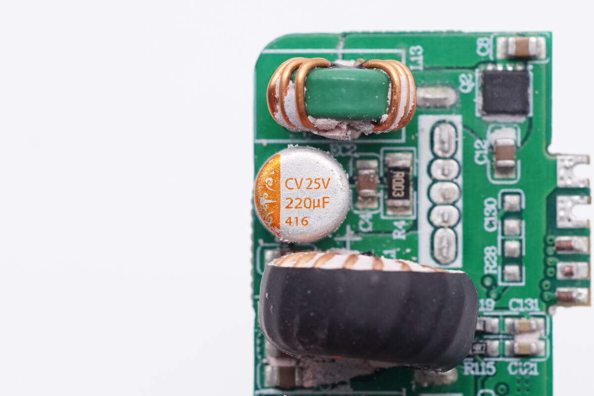
The filter capacitor is from CanCap. 25V 220μF.
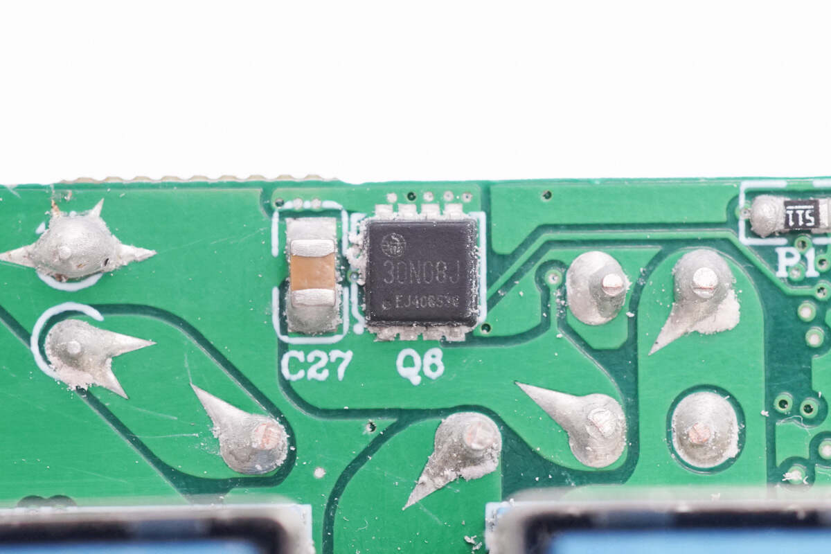
This VBUS MOSFET is from HRmicro. Model is HRT30N08J.
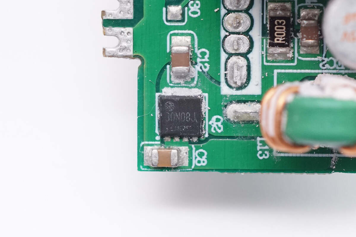
Another VBUS MOSFET is also from HRmicro. Model is HRT30N08J.
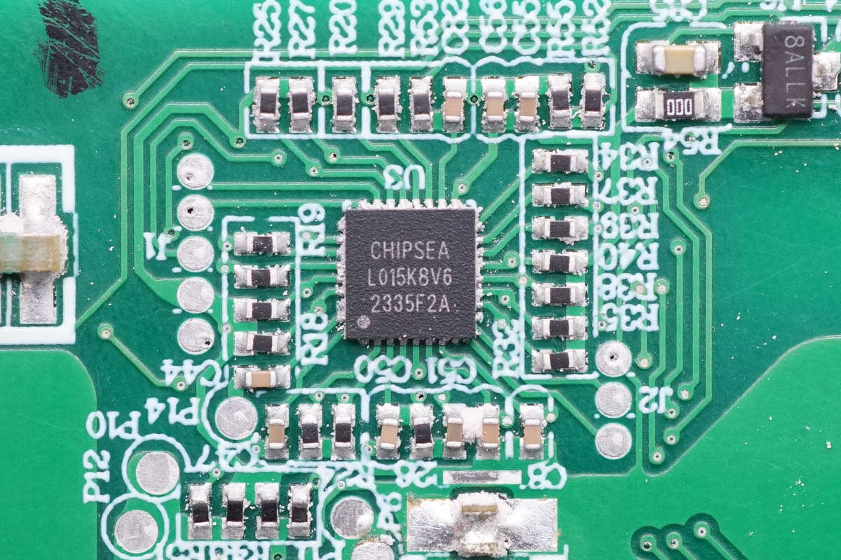
The MCU used for internal temperature detection and automatic power distribution control of the charger comes from Chipsea and adopts QFN32 package. It has a built-in ARM Cortex-M0+ CPU with a main frequency of 24MHz. Model is CS32L015K8V6.
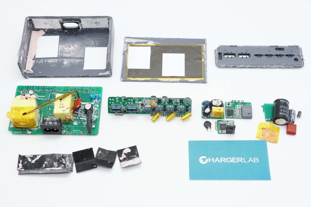
Well, those are all components of the Anker 200W desktop GaN charger.
Summary of ChargerLAB
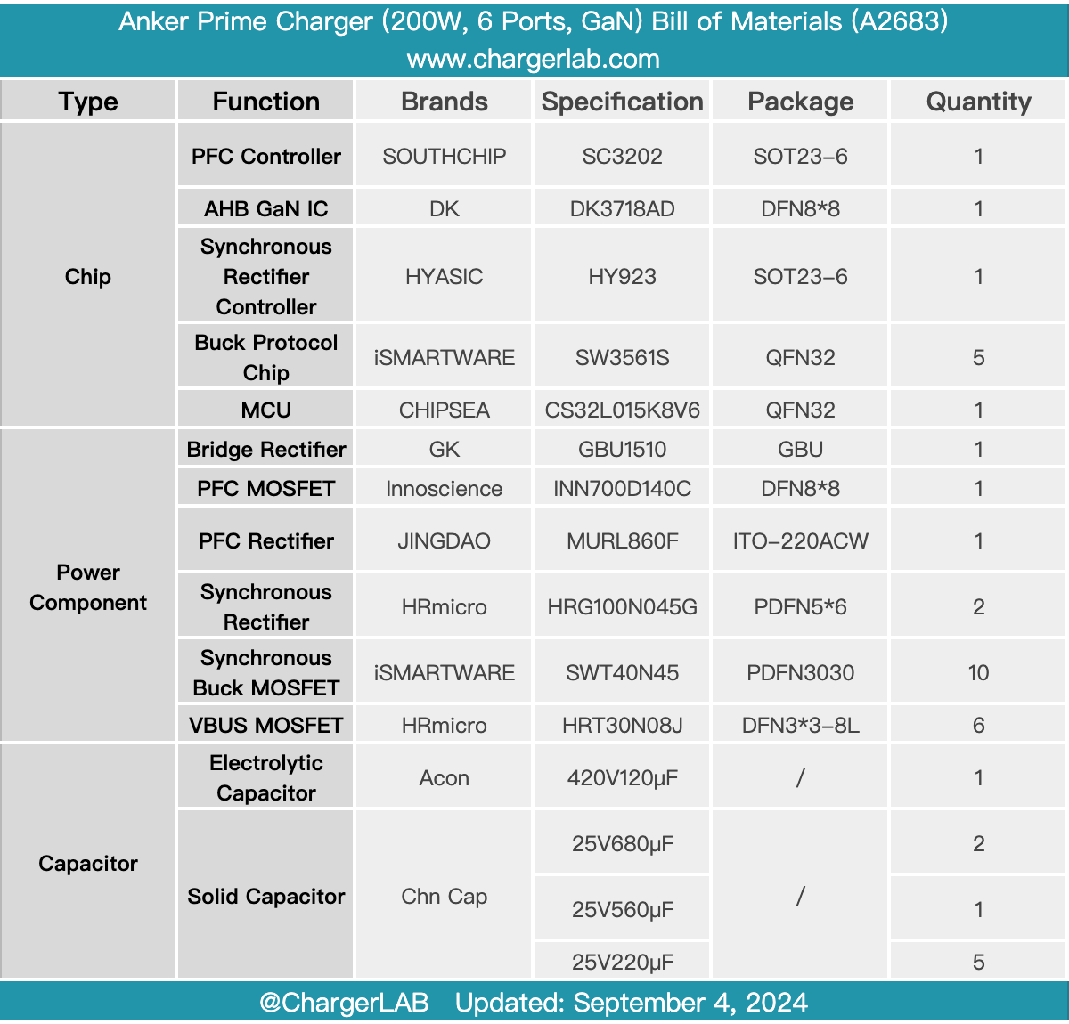
Here is the component list of the Anker 200W desktop GaN charger for your convenience.
It comes in a silver case with a black charging panel. It comes with four USB-C ports and two USB-A ports. All USB-C ports support 100W fast charging output and automatic power distribution. The USB-A port supports a charging power of 22.5W. It can charge your laptop, tablet, phone, headphones, and other devices at the same time, saving time.
After taking it apart, we found it adopts PFC+AHB design. It adopts five buck protocol chips. It is filled with pink potting compound to enhance heat dissipation. The overall workmanship and materials are solid.
Related Articles:
1. Trump Same Style | Teardown of Anker MagGo Magnetic Power Bank (Video)
2. Teardown of Anker 140W 2-in-1 USB-C to USB-C Cable (A8895)
3. Anker Launches 2-in-1 USB C to USB C Cable 140W Max

