Introduction
This time, ChargerLAB got a 3-in-1 GaN charger from Anker. It has a USB-A and two USB-C ports. It also comes with foldable prongs. And it can support a charging power of up to 65W even in its small size. Both USB-C ports can support 65W PD and PPS. Next, let's take it apart to see the internal components.
Product Appearance
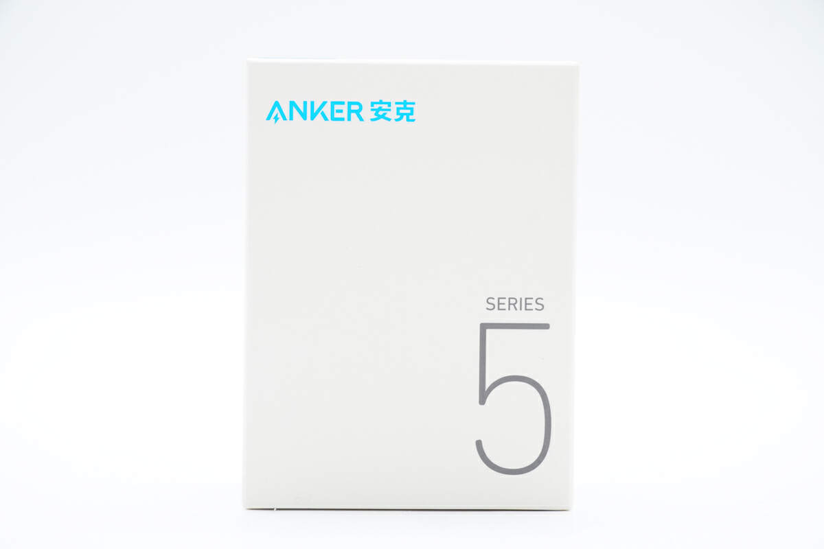
The "ANKER" is printed on the box.
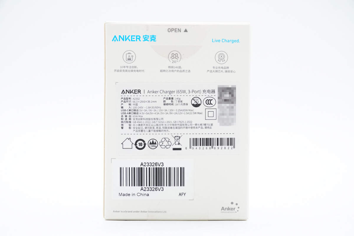
And the back has specs info, which we'll talk about later.
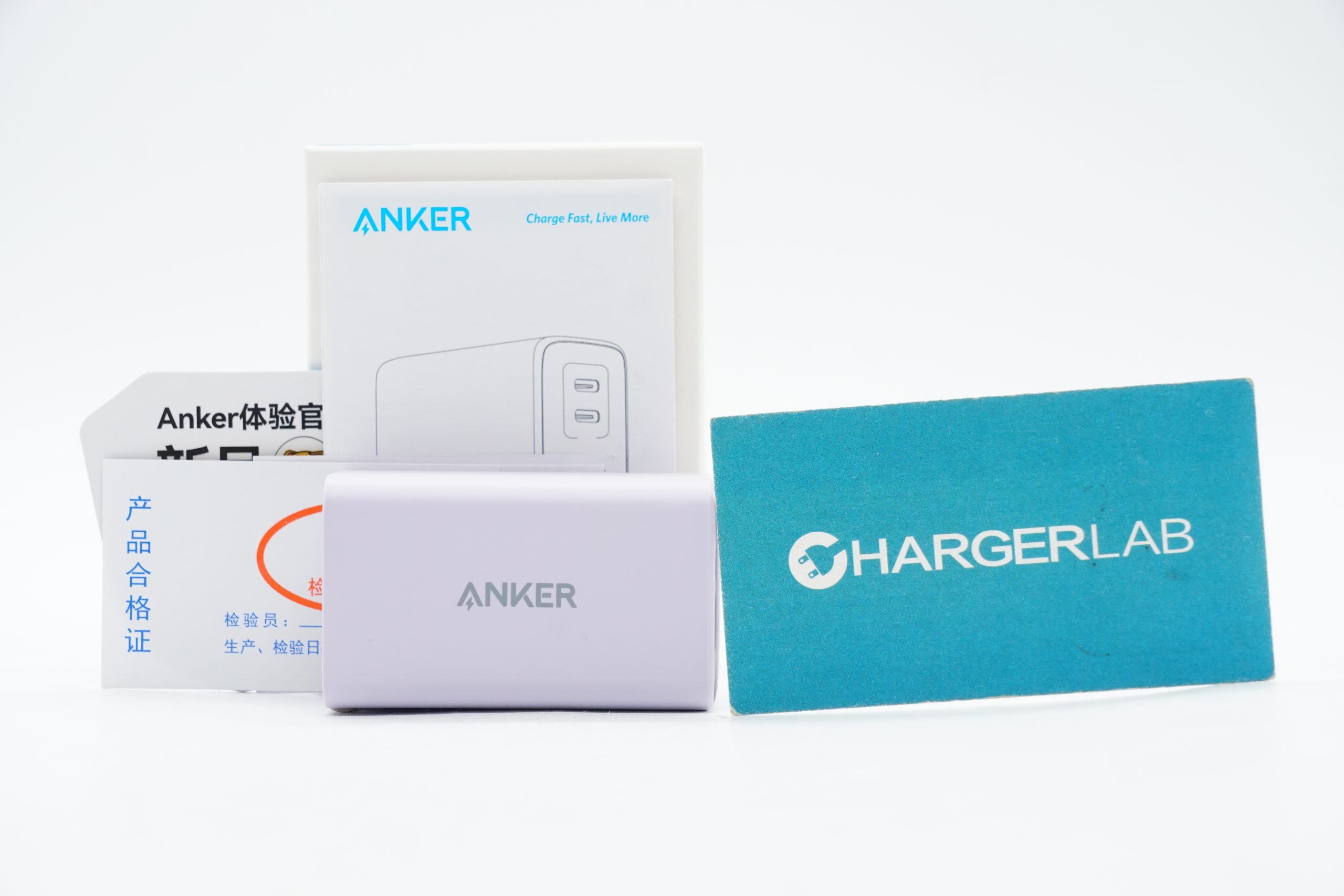
The box contains the charger and some documents.
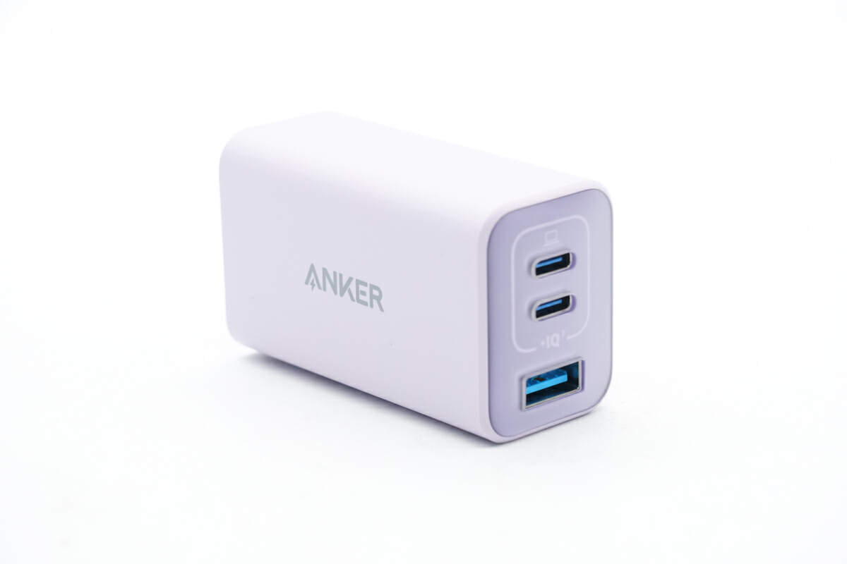
The charger adopts a rounded case.

The case is made of the fire retardant PC. And this side has the logo of Anker.
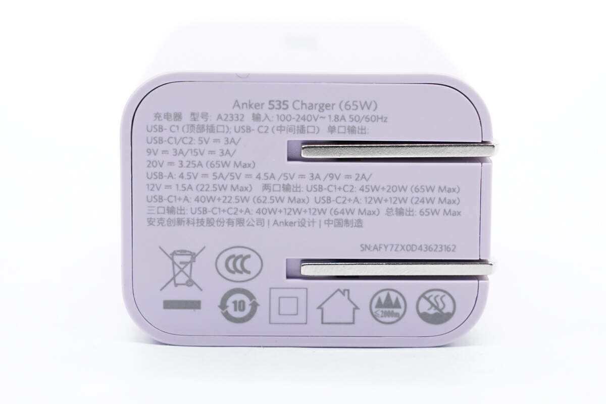
The specs info are also printed on the input end. Model is A2332. It can support input of 100-240V~50/60Hz 1.8A. The maximum charging power of the USB-C1, USB-C2, and USB-A are 65W, 65W, and 22.5W, respectively. The total output is 65W.
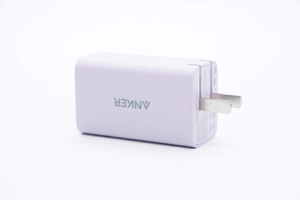
It comes with the foldable prongs.
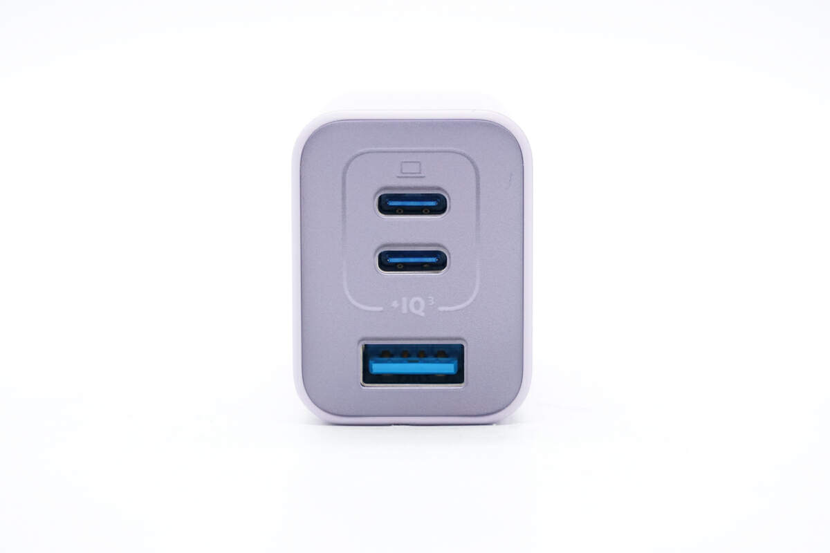
The output panel has a USB-A and two USB-C ports. The plastic sheets are blue.
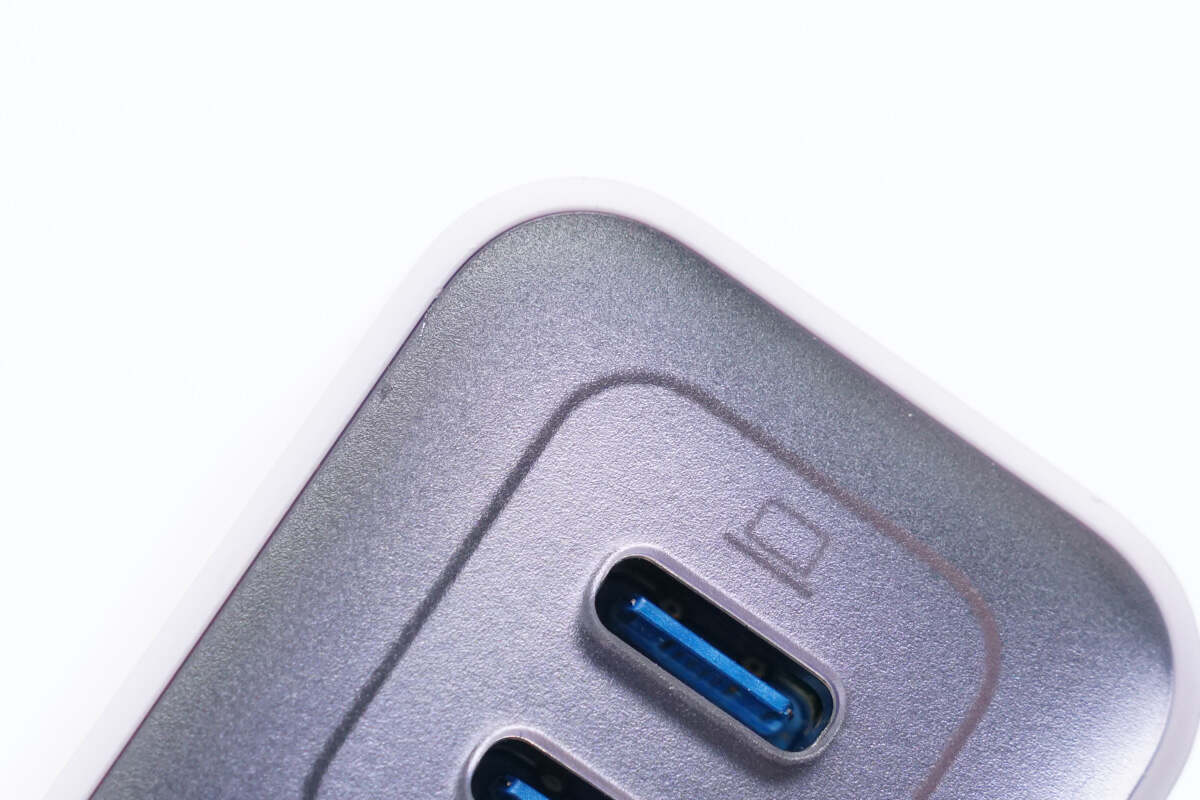
The output cover has a translucent design.
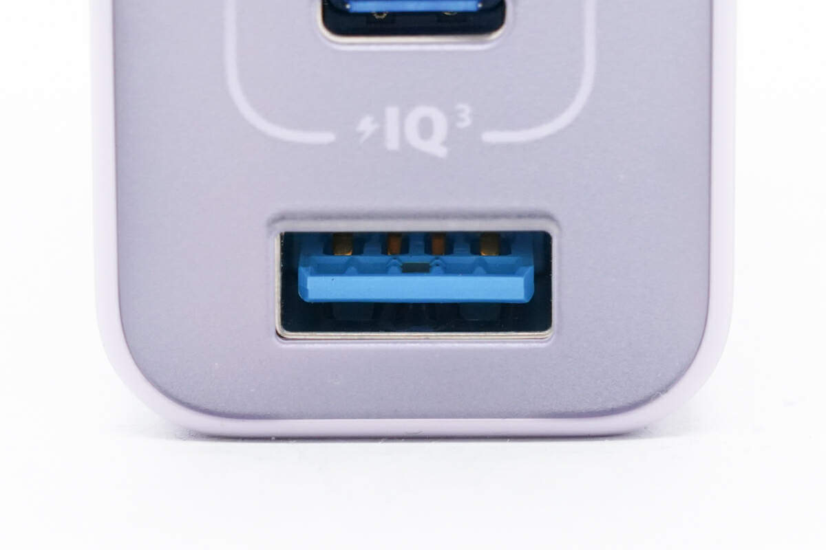
The USB-A port has special pins.
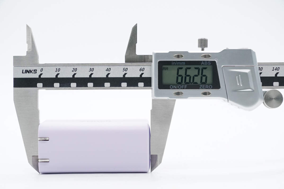
The length is about 66 mm (2.6 inches).
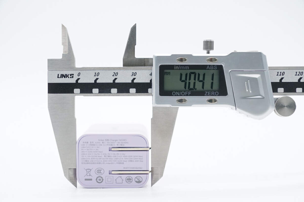
The width is about 40 mm (1.57 inches).
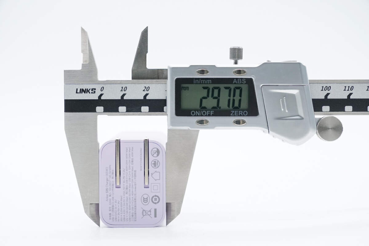
The thickness is about 30 mm (1.18 inches).
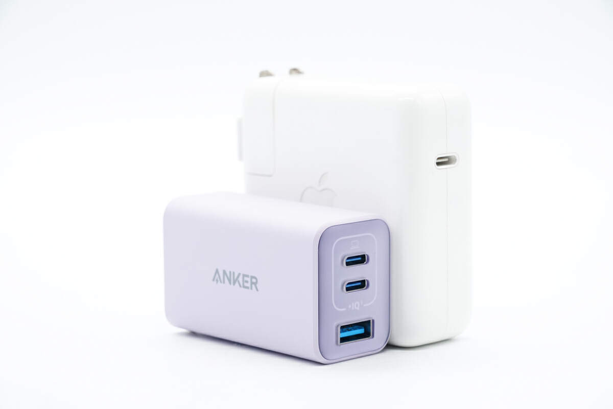
It's much smaller than the Apple 61W charger.

That's how big it is in the hand.
And the weight is about 133 g (4.69 oz).
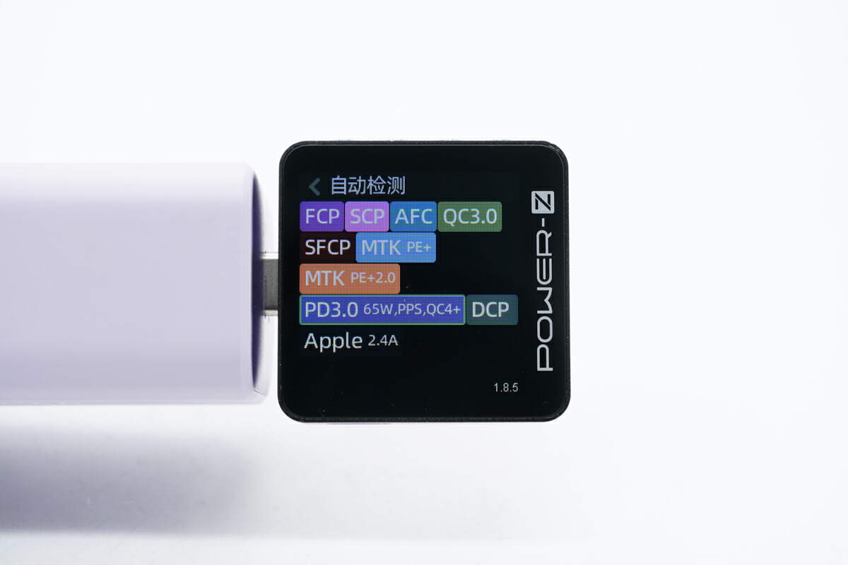
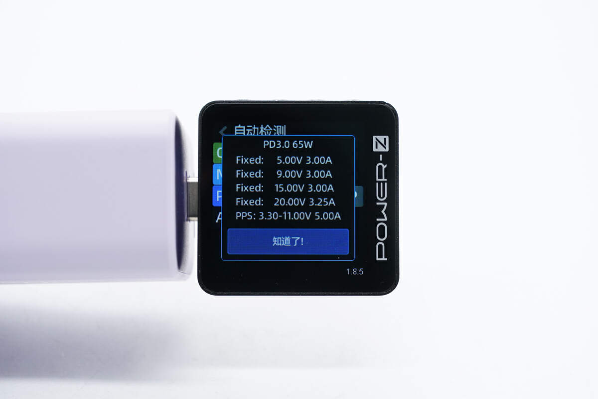
The ChargerLAB POWER-Z KM003C shows that the USB-C1 supports FCP, SCP, AFC, QC3.0/4+, SFCP, PE2.0, PD3.0, PPS, DCP, and Apple 2.4A protocols.
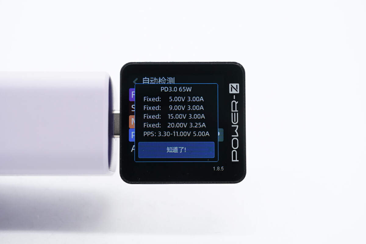
And it has four fixed PDOs of 5V3A, 9V3A, 15V3A, and 20V3.25A, and a set of PPS, which is 3.3-11V5A.
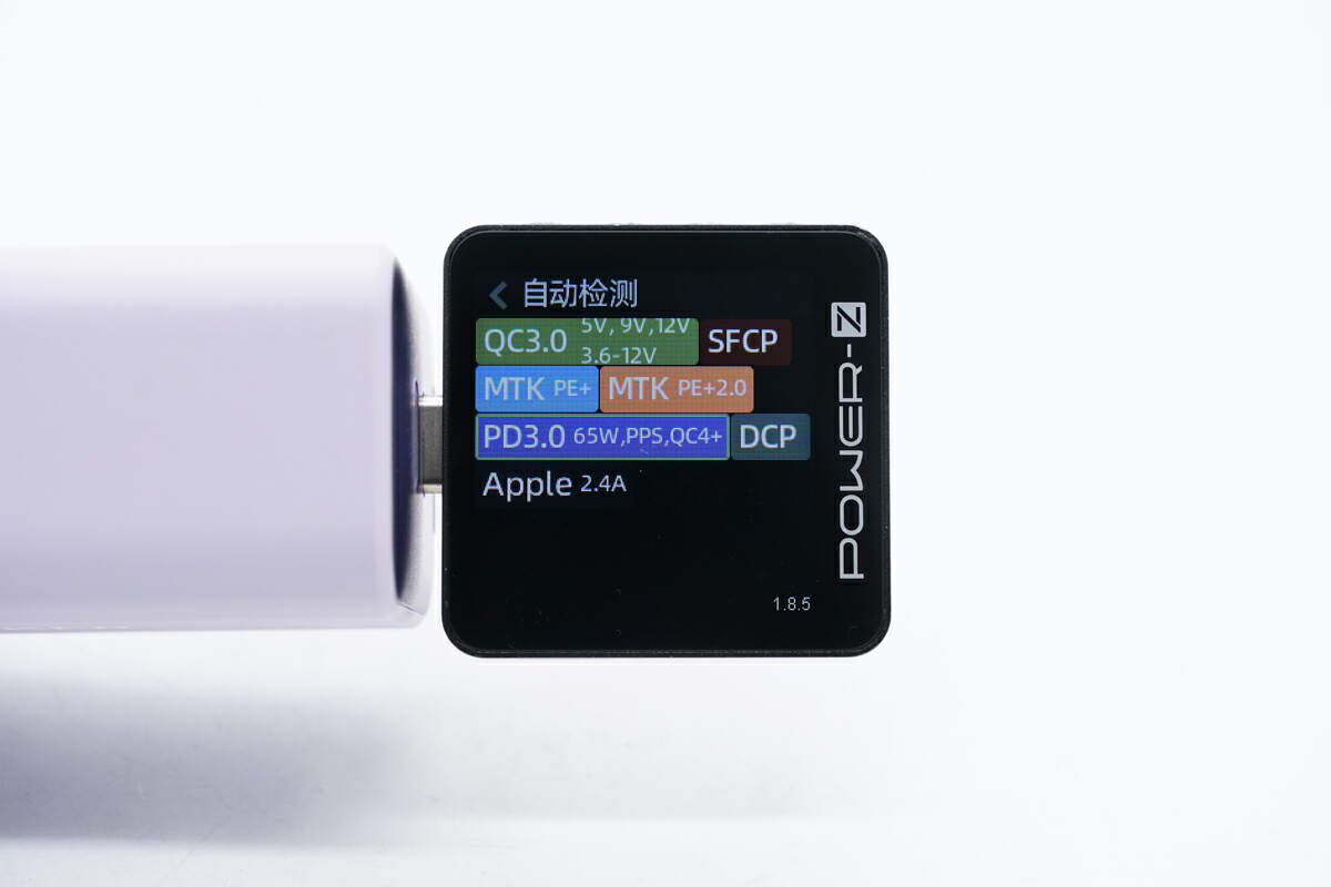
The supported protocols of USB-C2 are QC3.0/4+, SFCP, PE2.0, PD3.0, PPS, DCP, and Apple 2.4A charging protocols.
And it has four fixed PDOs of 5V3A, 9V3A, 15V3A, and 20V3.25A, and a set of PPS, which is 3.3-11V5A.
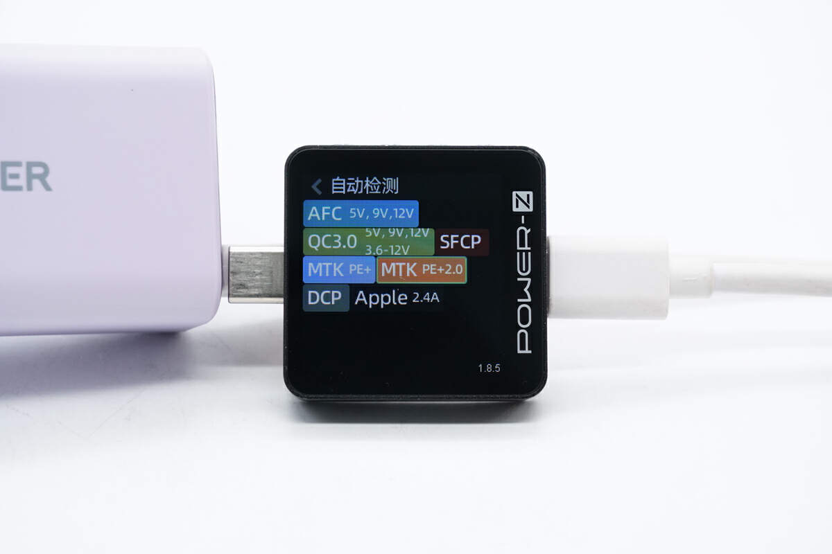
The USB-A supports AFC, QC3.0, SFCP, PE2.0, DCP, and Apple 2.4A charging protocols.
Teardown
Now, let's start to take it apart.
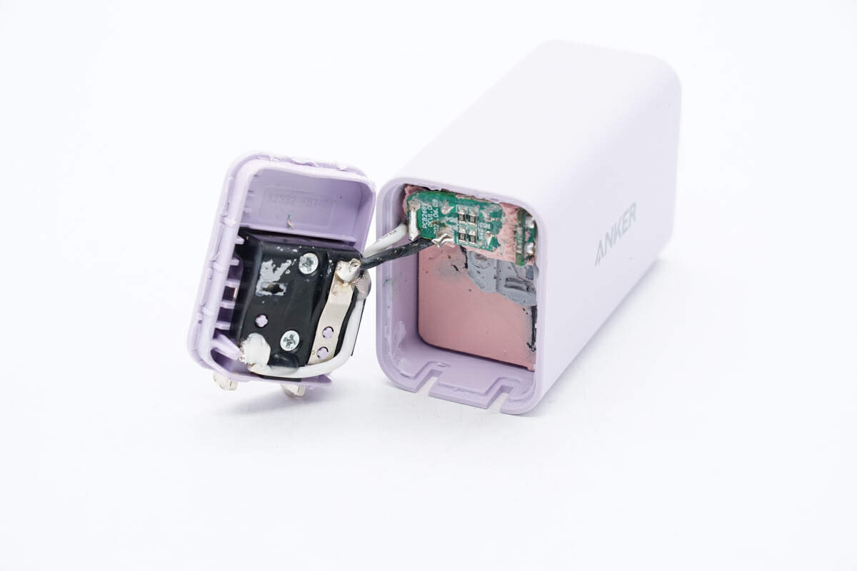
Remove the input cover along the gap.
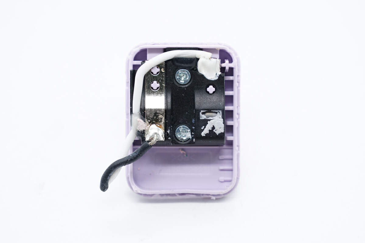
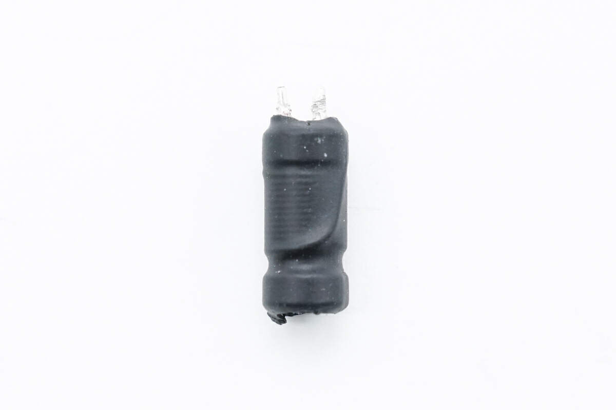
The plugs are connected to the PCB through wires.
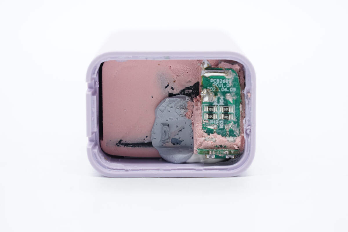
The PCBA module is filled with potting compound.
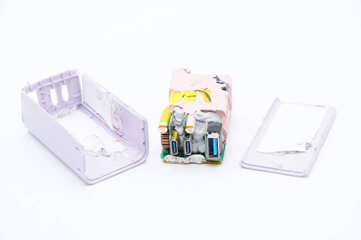
Take out the PCBA module.

There are thermal pads pasted inside the case.
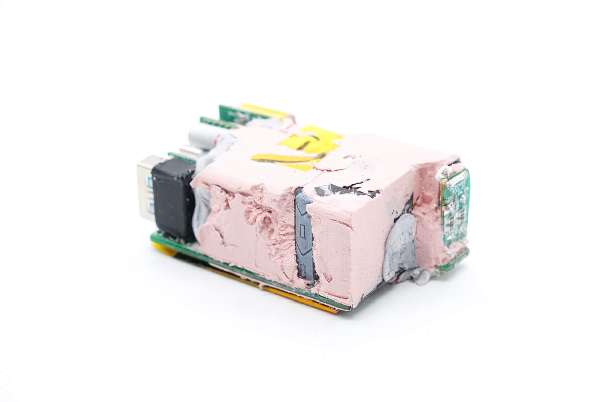
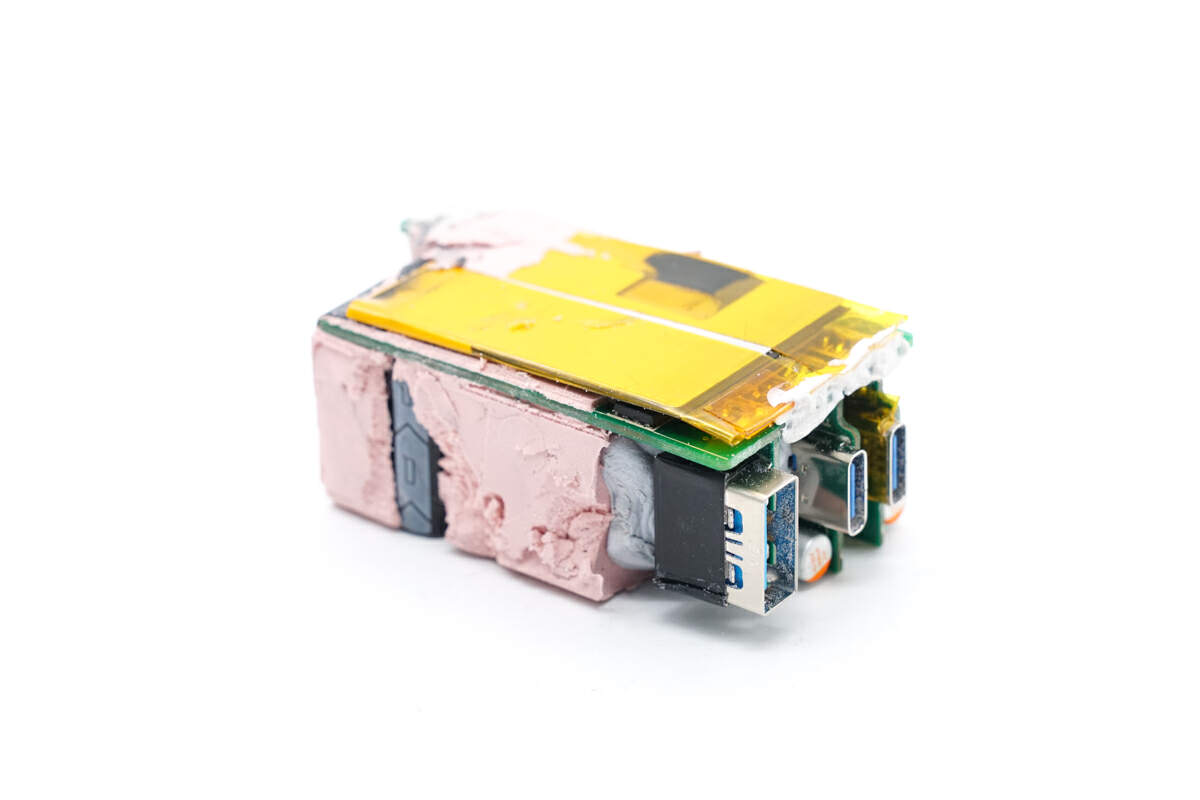
The entire PCBA module is covered and filled with pink potting compound for heat dissipation.
The heat sink on the back is fixed with heat-resistant tape.
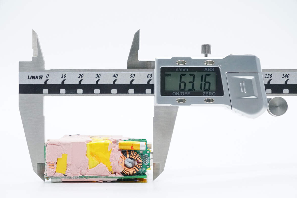
The length of the PCBA module is about 63 mm (2.48 inches).
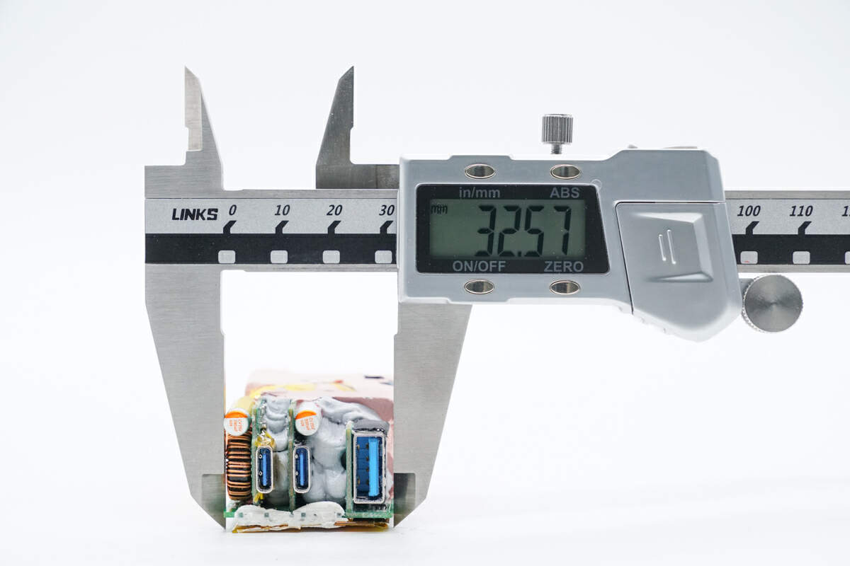
The width is about 33 mm (1.3 inches).
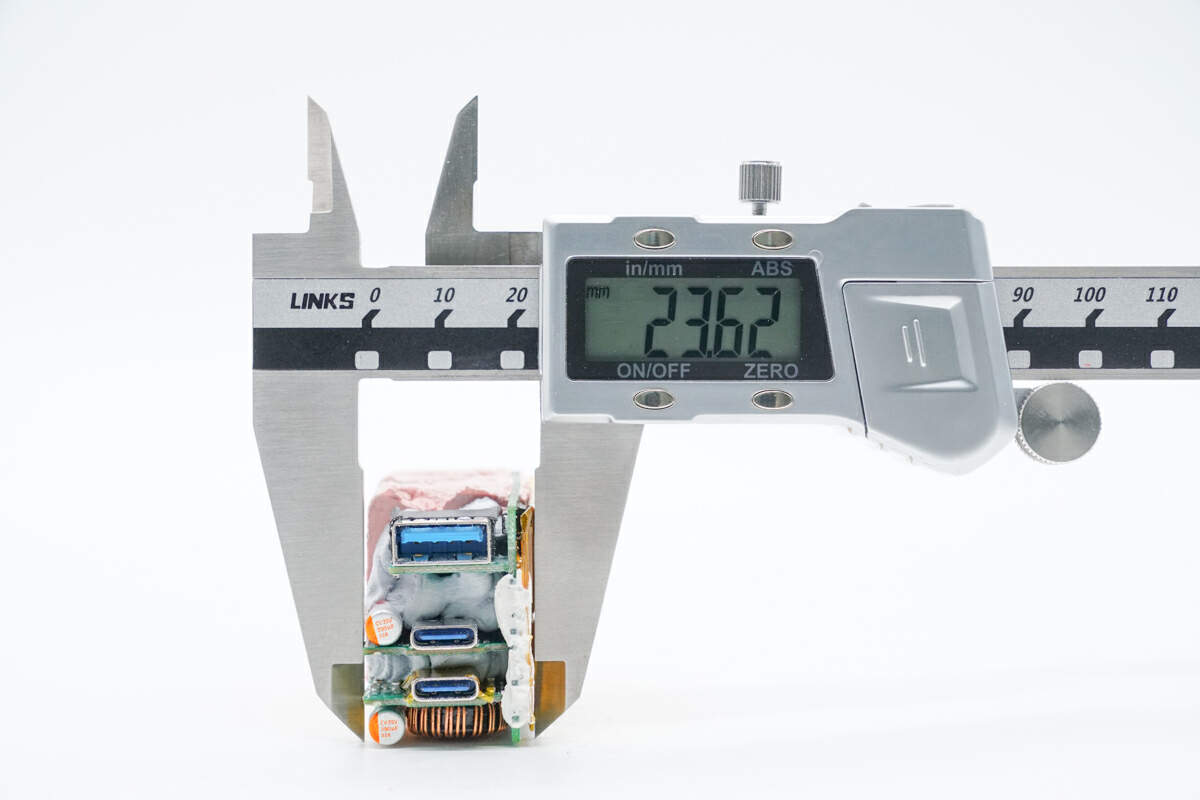
The thickness is about 24 mm (0.94 inches).
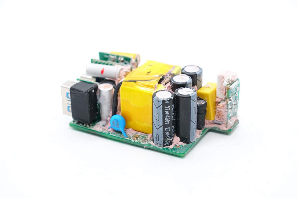
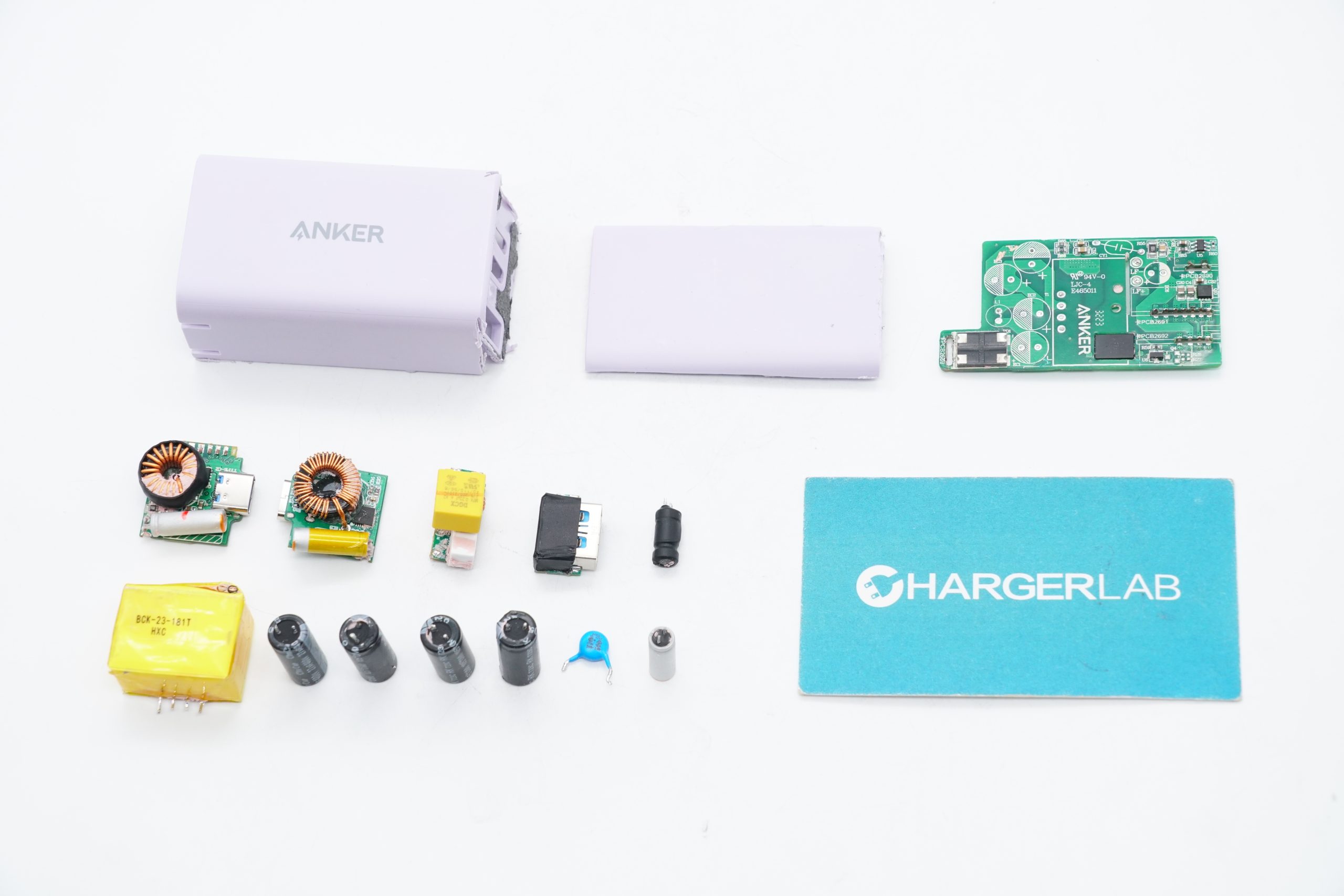
Clean up the PCBA module.
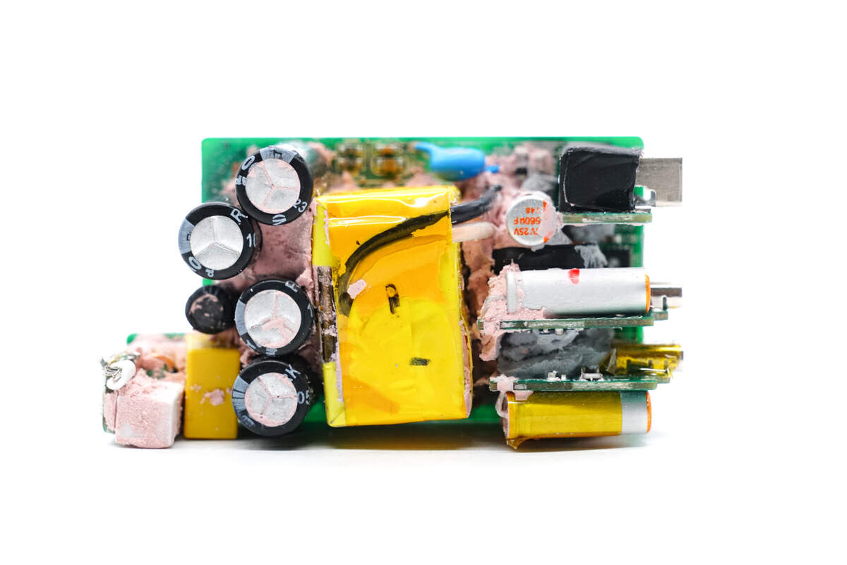
There are fuse, common mode choke, safety X2 capacitor, capacitors, and buck PCBs on the front.
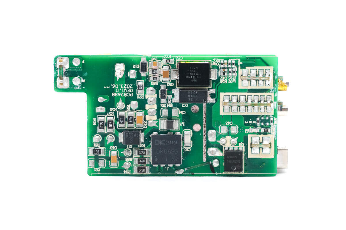
The master control chip, optocoupler, SMD Y capacitor, and synchronous rectifier are on the back.
ChargerLAB found it adopts two independent buck circuits to achieve three-port fast charging and automatic power distribution.
Next, we will take a look at each component starting from the input end.
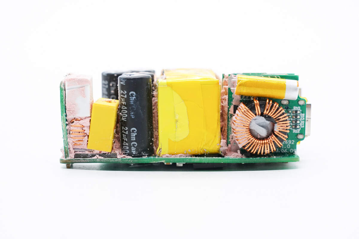
There are transformer, capacitor, and buck PCBs on the side of the PCBA.
A small PCB is soldered vertically on the input end.
The fuse, common mode choke, and safety X2 capacitor are on the front of this small PCB.
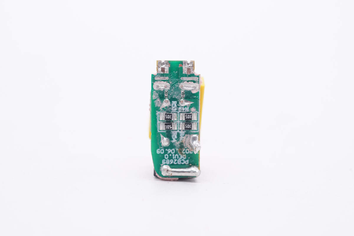
The back has resistors of the safety X2 capacitor.
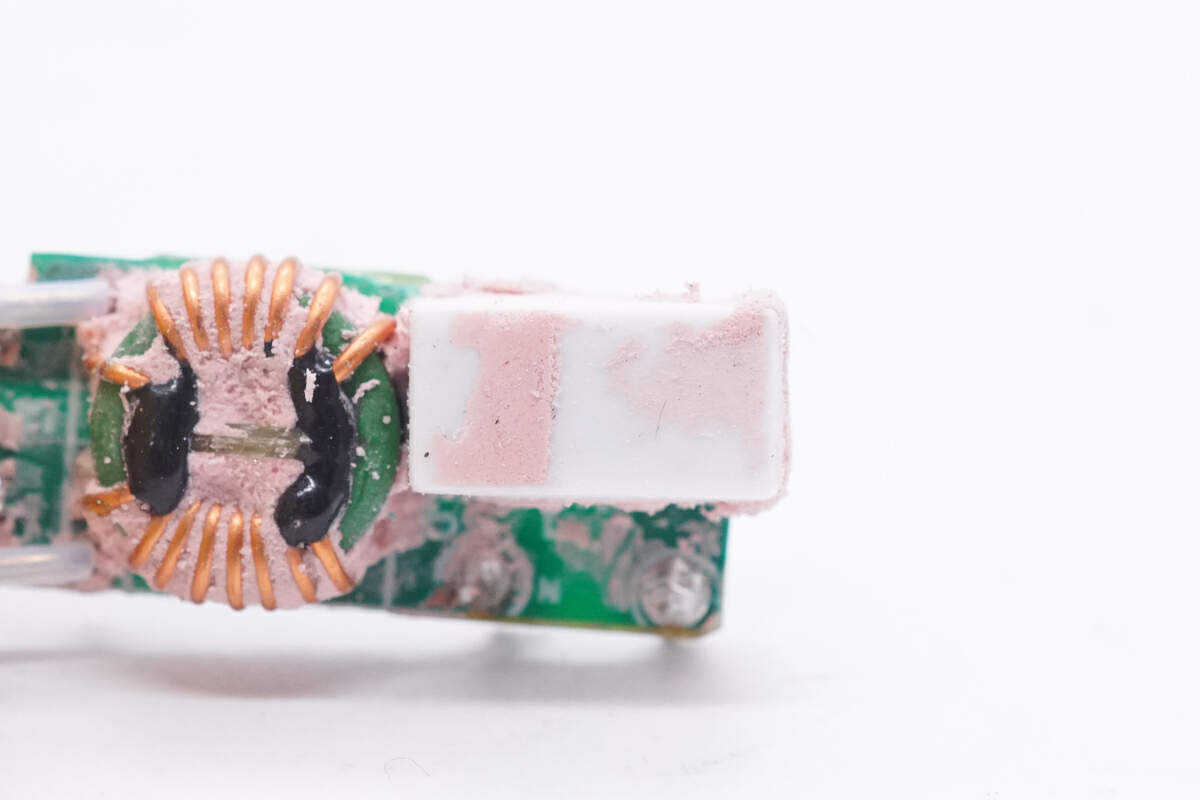
The fuse is insulated by the white rubber cover.
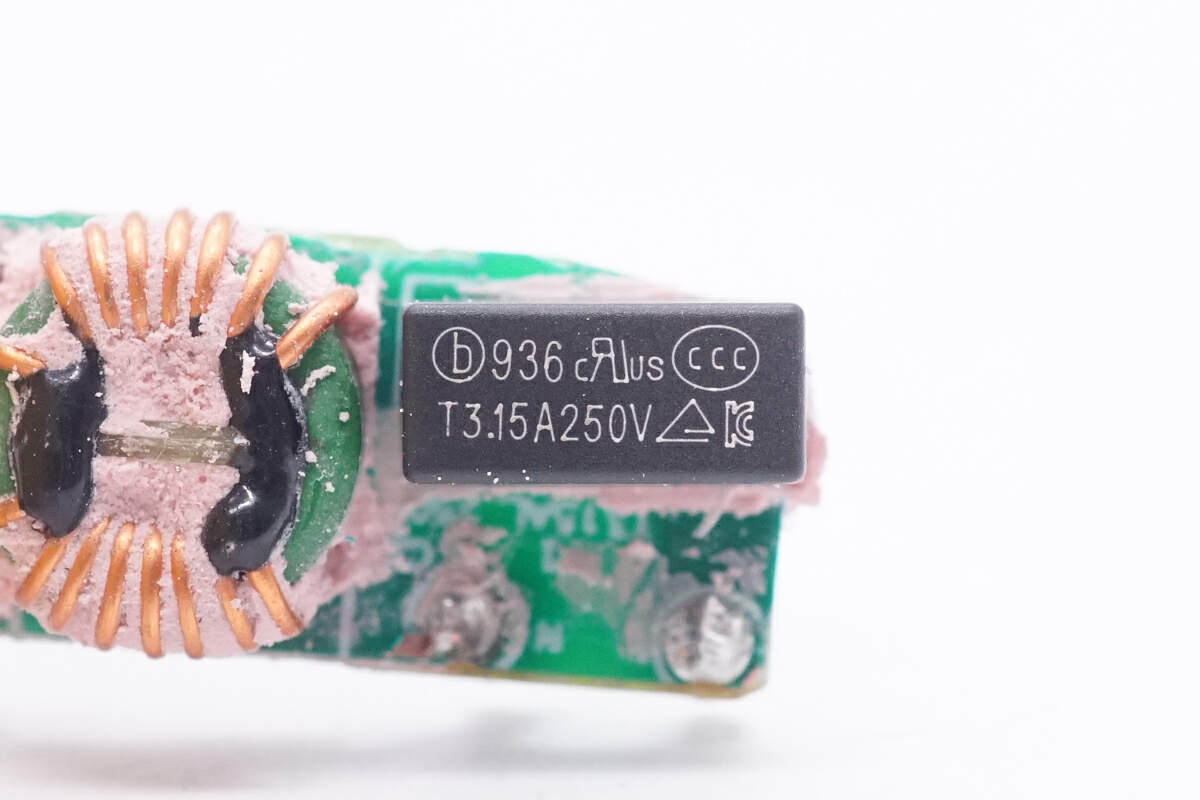
Take off the rubber cover. The fuse is from Betterfuse. 3.15A 250V.
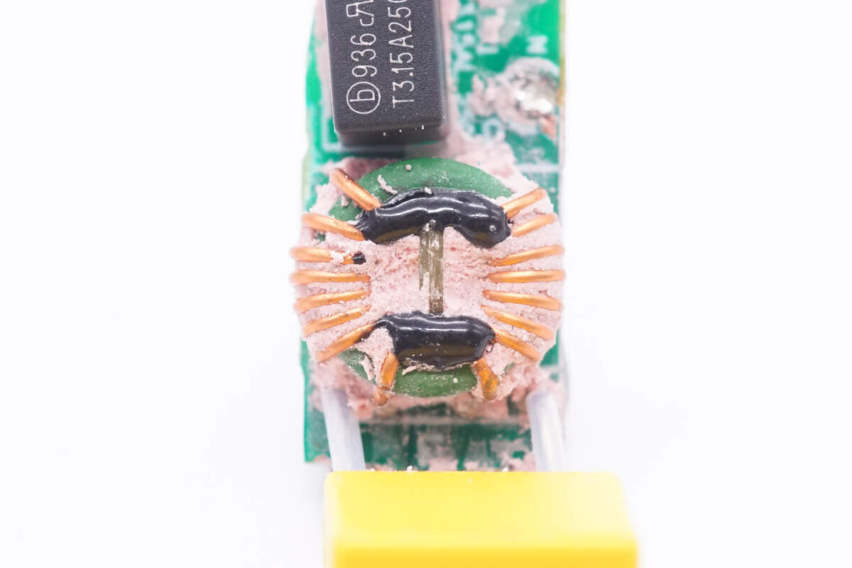
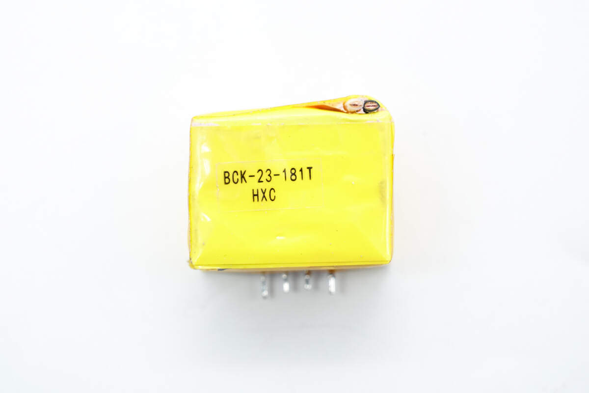
The common mode choke is wound with magnet and insulated wires, and it's also insulated with bakelite.
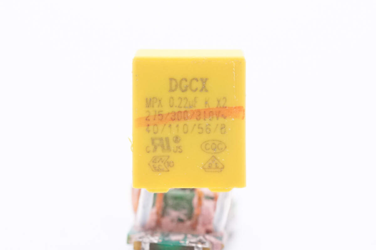
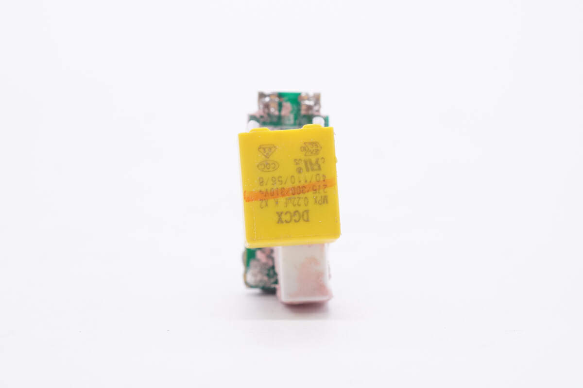
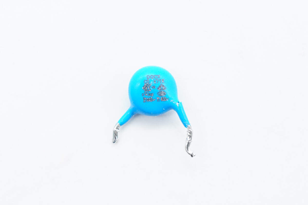
The safety X2 capacitor is from DGCX. 0.22μF.
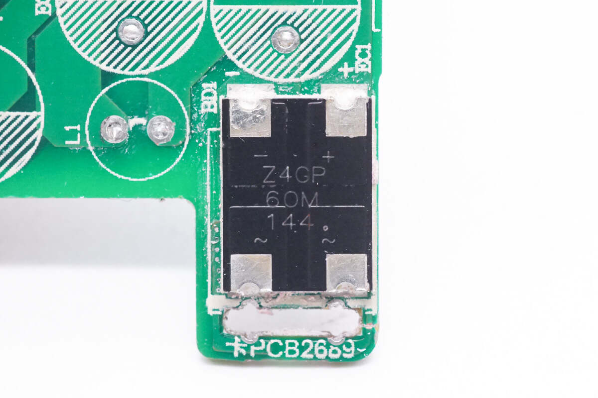
The bridge rectifier is from ZOWIE. Model is Z4GP60M. 1000V 6A.
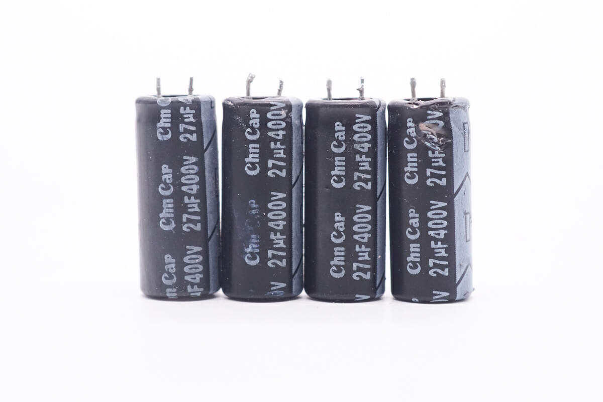
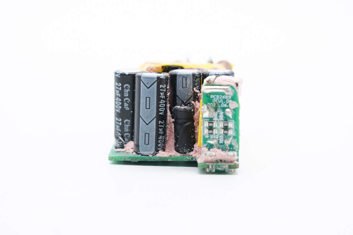
These four electrolytic capacitors for input filtering are from Chn Cap. The total capacity is 108μF. 27μF 400V.
The differential mode chock is insulated by heat-shrinkable tubing.
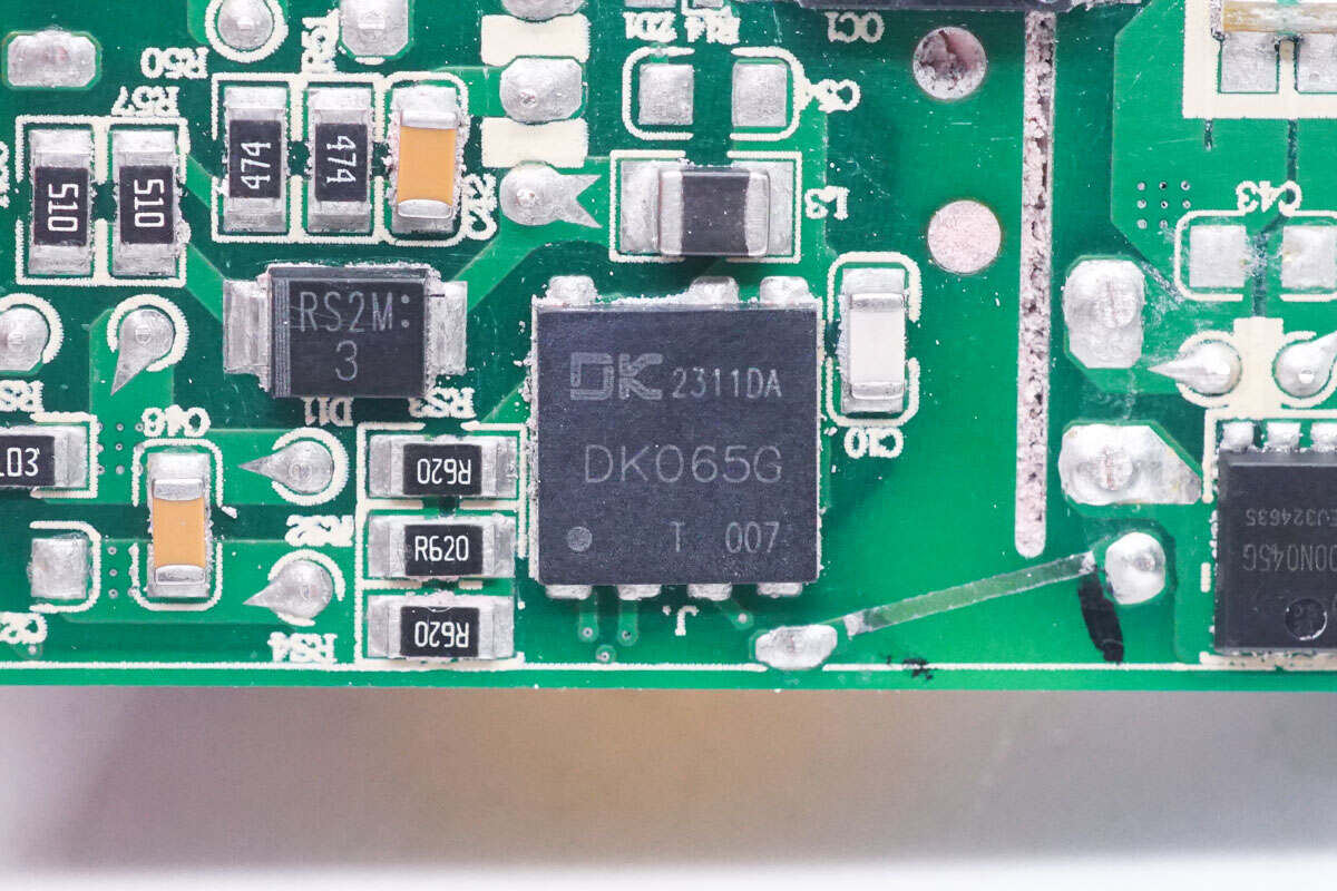
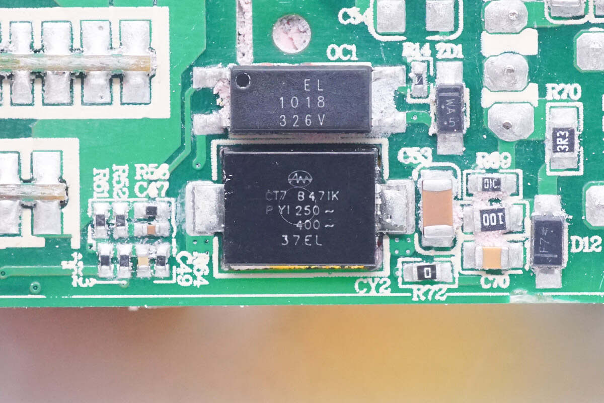
The master control chip is from DONGKE. It integrates flyback controller and a GaN FET which is 650V 260mΩ. It supports output voltage, power supply voltage, overheating protection, and other protection functions. Model is DK065G.
The magnetic core of the transformer is insulated by tape.
The blue Y capacitor is from DGCX.
The SMD Y capacitor is from KeiFat. It is placed in the opening of the PCB to reduce thickness.
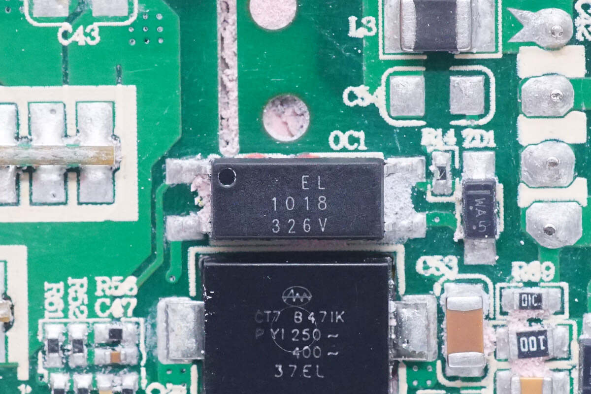
The optocouple is from Everlight and is used for output voltage feedback. Model is EL1018.
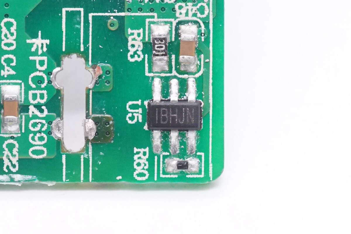
The synchronous rectifier controller marked with IBHJN is from MPS. It can support a frequency of up to 600KHz. It also supports DCM, CCM, QR, and ACF working modes. Model is MP6908A.
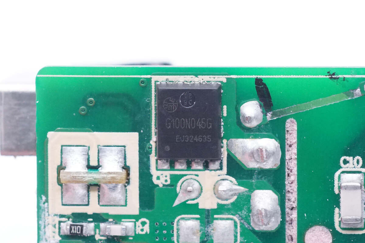
The synchronous rectifier is from HRmicro and adopts PDFN5 x 6 package. Model is HRG100N045G. 100V 3.4mΩ.
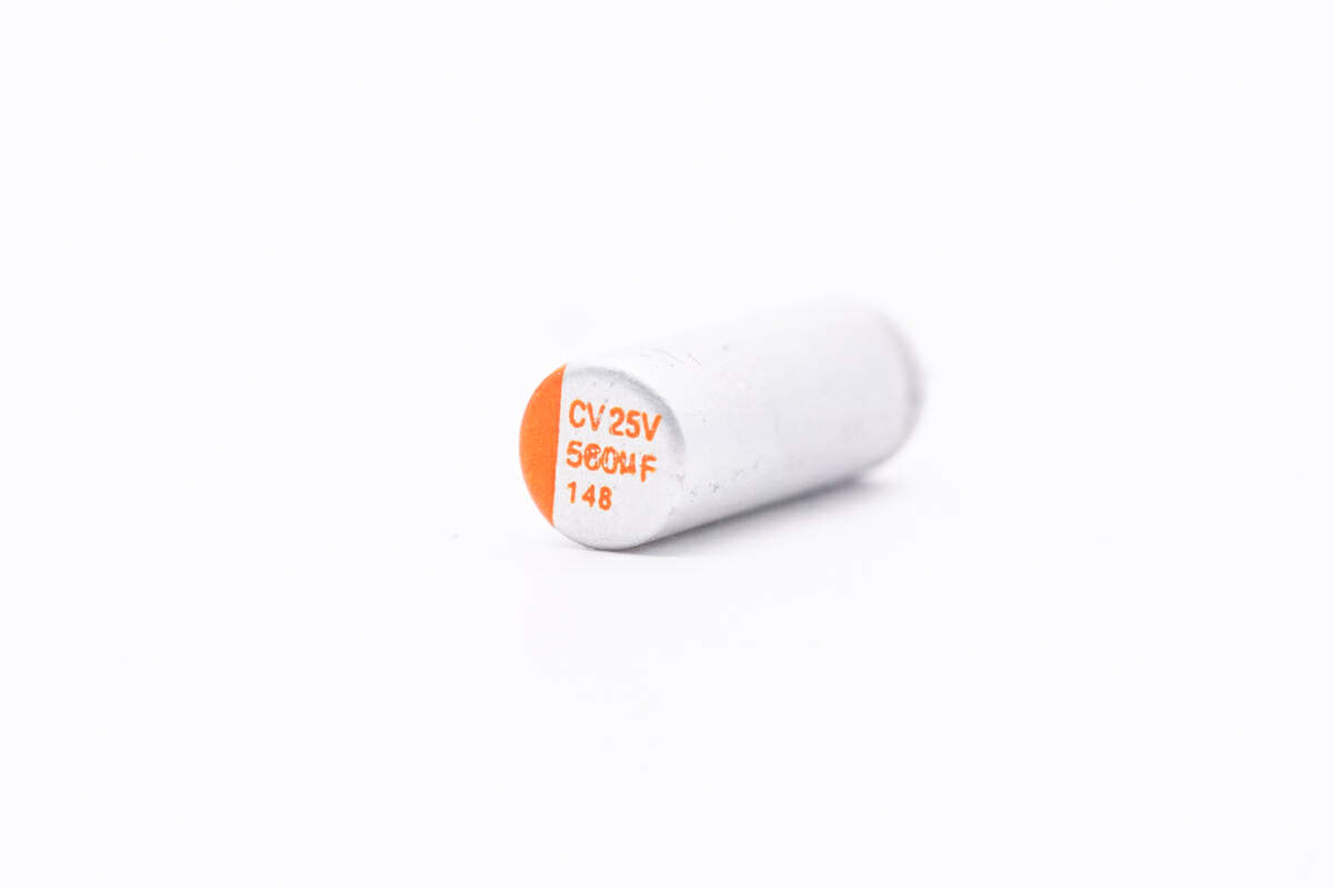
The solid capacitor for output filtering is from Chn Cap. 25V 560μF.
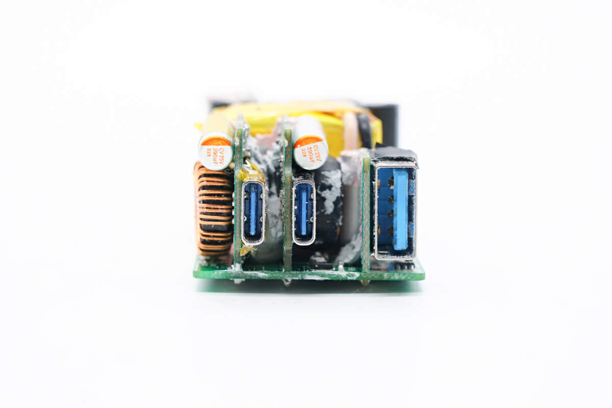
The output end has three small PCBs.
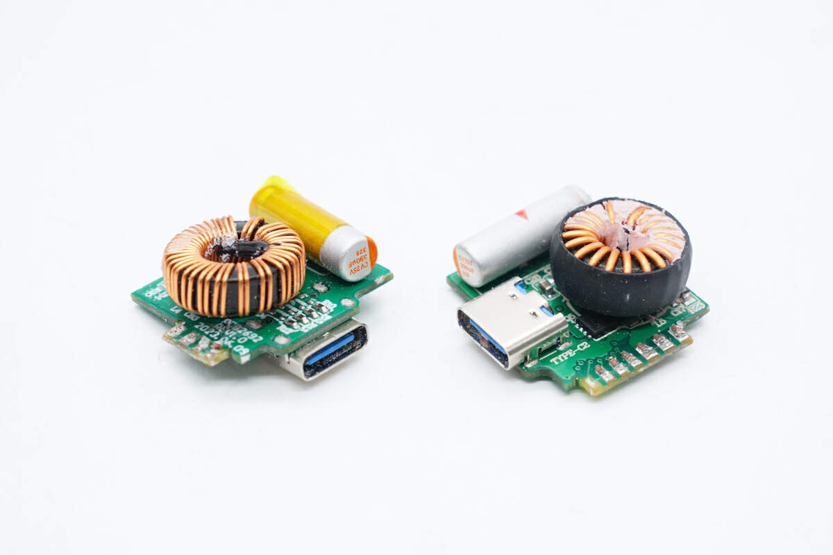
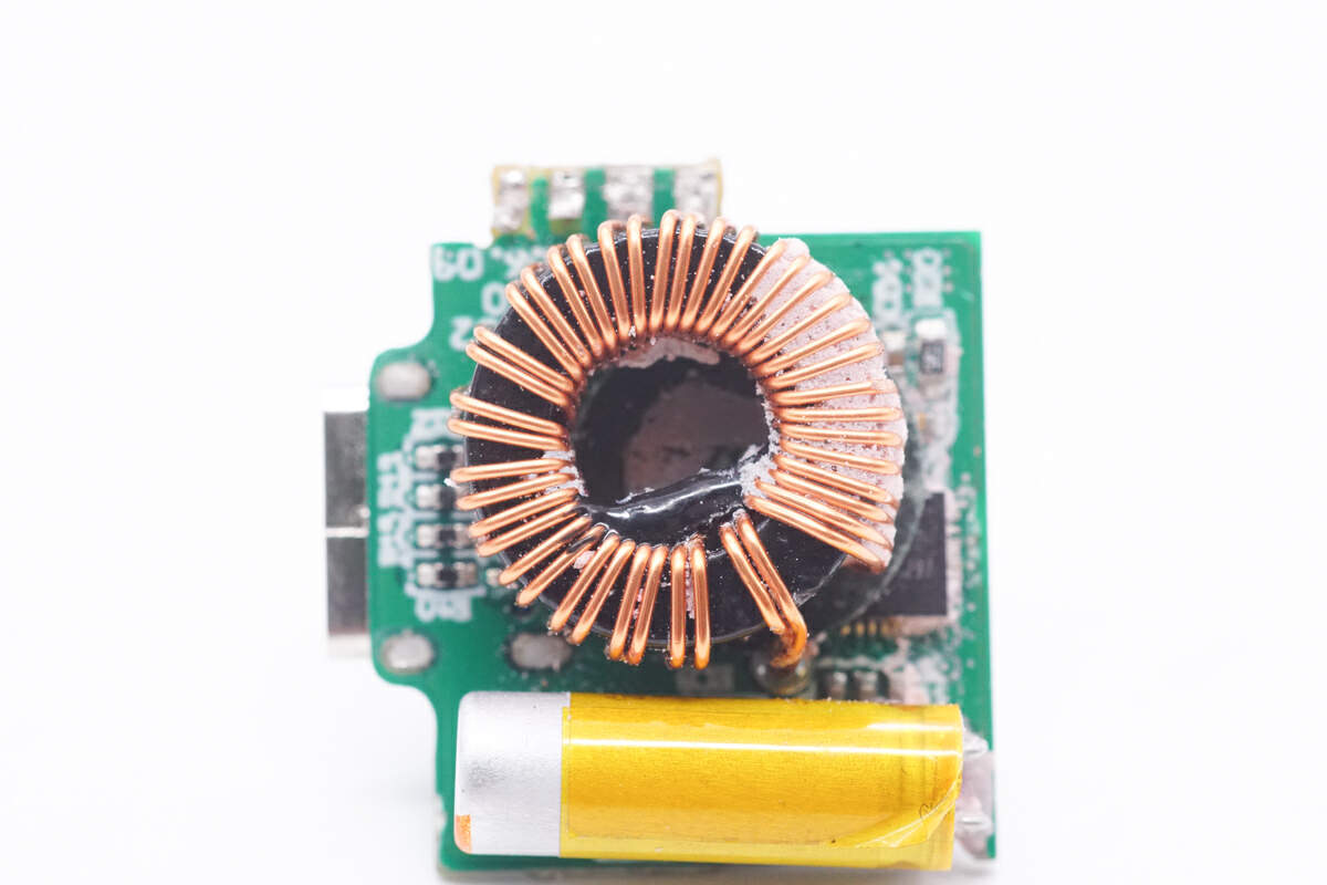
There are buck PCBs of USB-C1, C2, and USB-A. The inductor of USB-C2 and USB-A is wrapped in heat-shrinkable tubing.
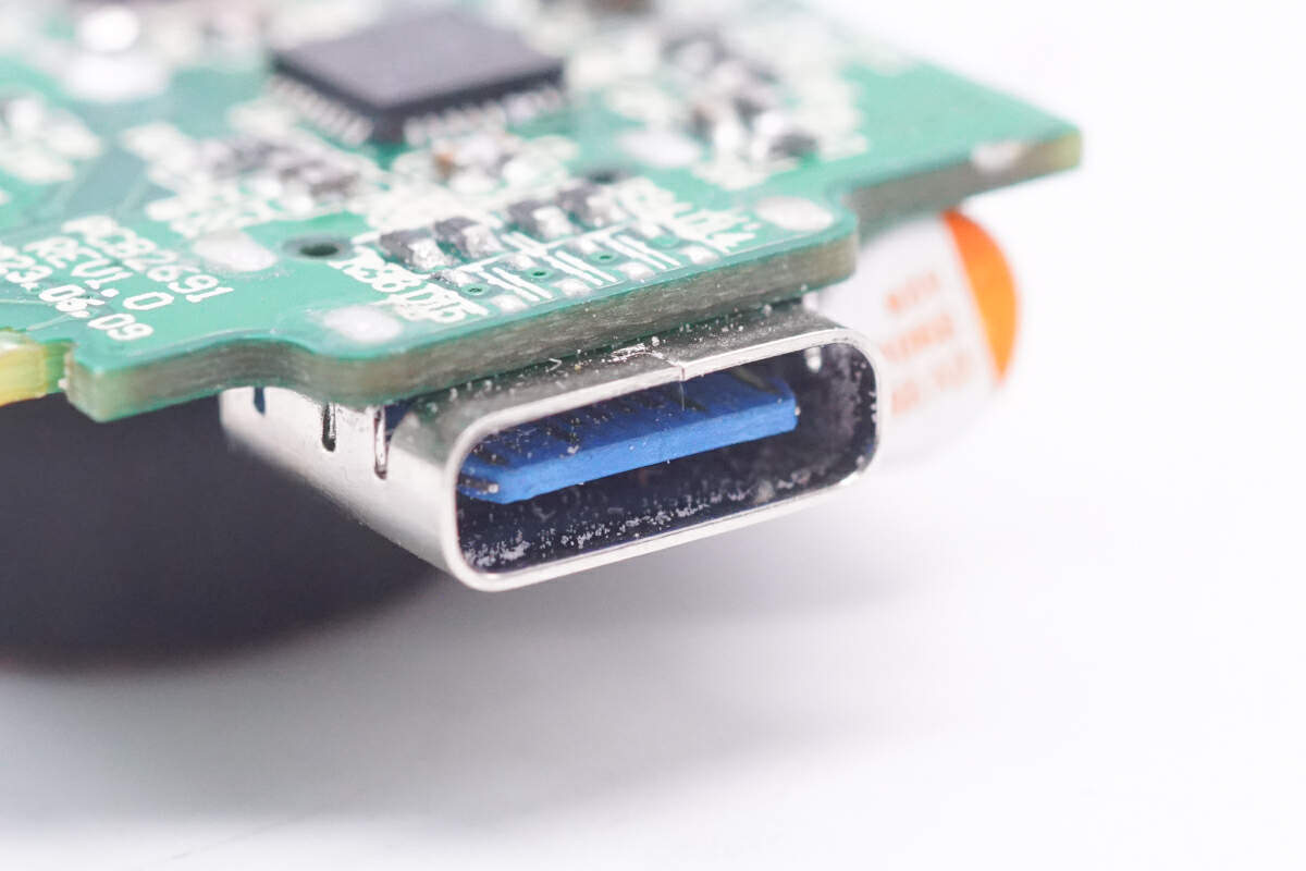
There is a buck inductor and a solid capacitor on the buck PCB of USB-C1. The solid capacitor for output filtering is insulated by tape.
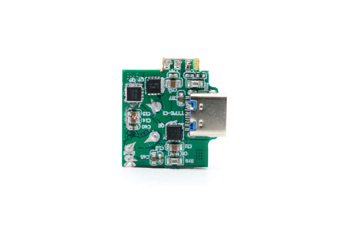
The back has a USB-C socket and MOSFETs.
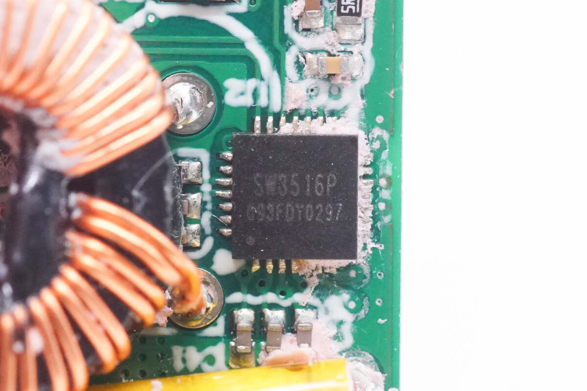
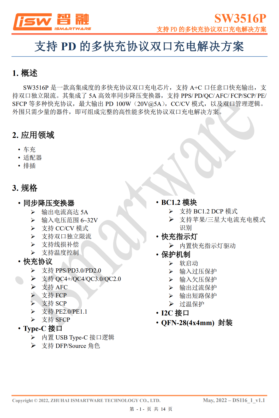
The buck controller is from iSmartWare. It supports charging of any USB-C and USB-A ports and dual-port independent current limiting. Model is SW3516P.
It integrates a 5A high-efficiency synchronous buck converter. It supports PPS, PD, QC, AFC, FCP, SCP, PE, SFCP, and other fast-charging protocols. It can output up to PD 100W. It also supports CC/CV modes.
Here is all the information about the iSmartWare SW3516P.
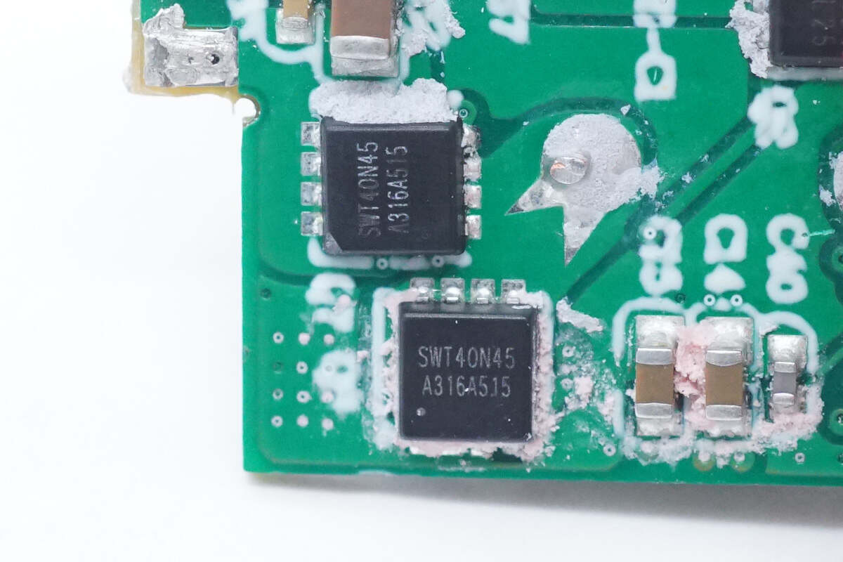
The MOSFET used for secondary synchronous buck circuit is from iSmartWare. Model is SWT40N45.
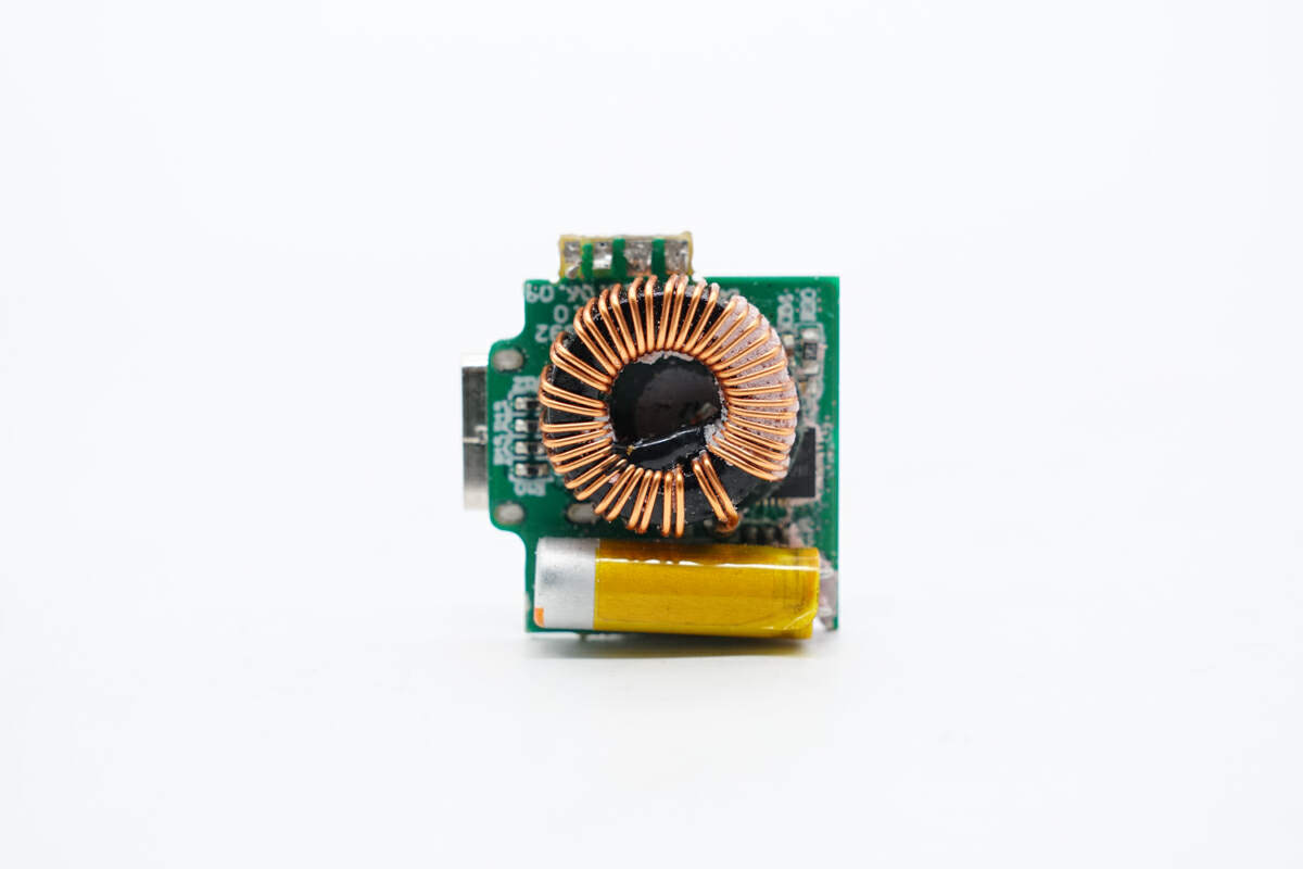
The buck inductor is wound with wires.
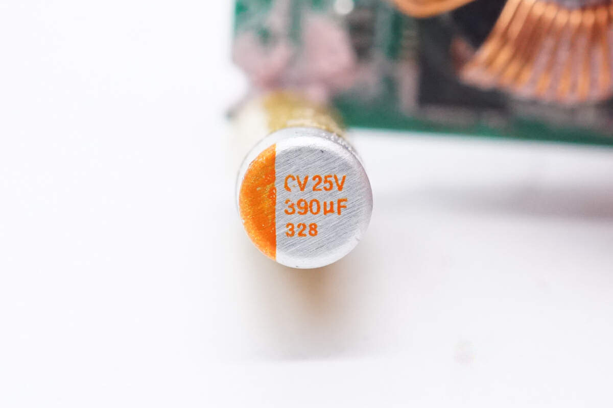
The solid capacitor for output filtering is from Chn Cap. 25V 390μF.
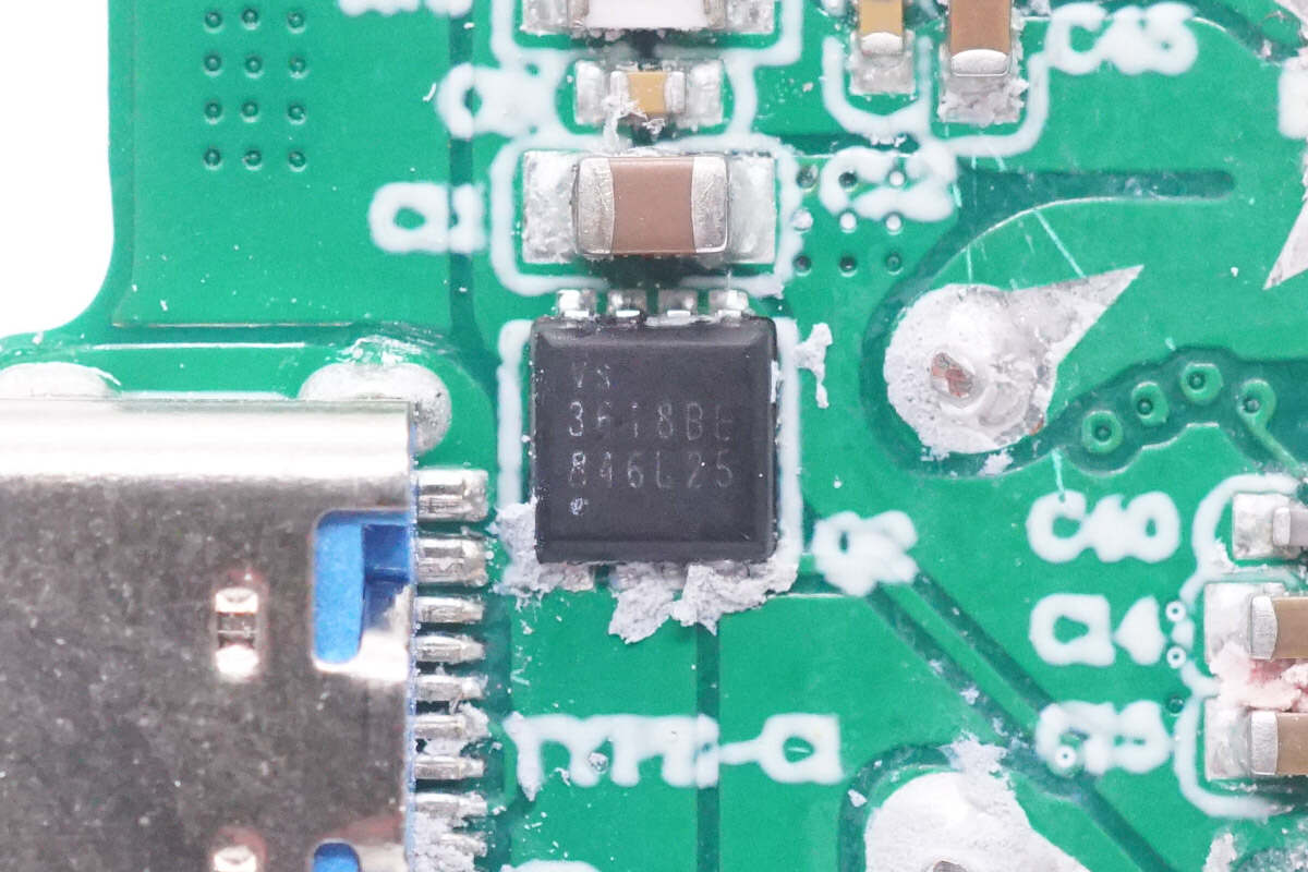
The VBUS MOSFET is from VGSEMI and adopts PDFN3333 package. Model is VS3618BE. 30V 5.2mΩ.
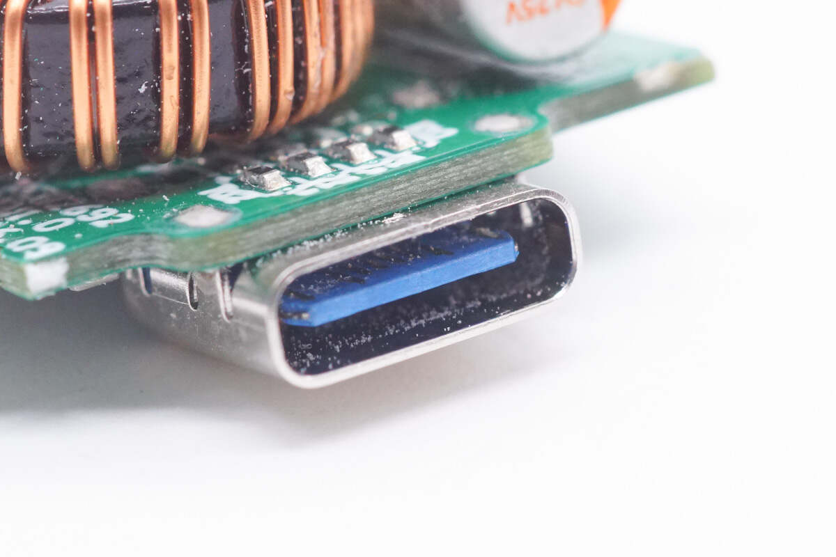
The USB-C1 socket has a blue plastic sheet.
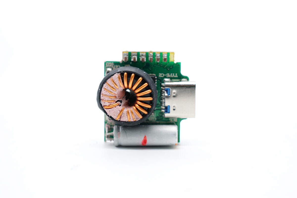
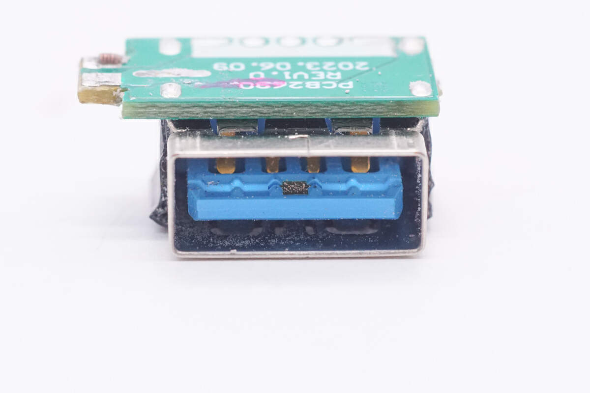
The socket, buck inductor, and capacitor are on the PCB of USB-C2 and USB-A.
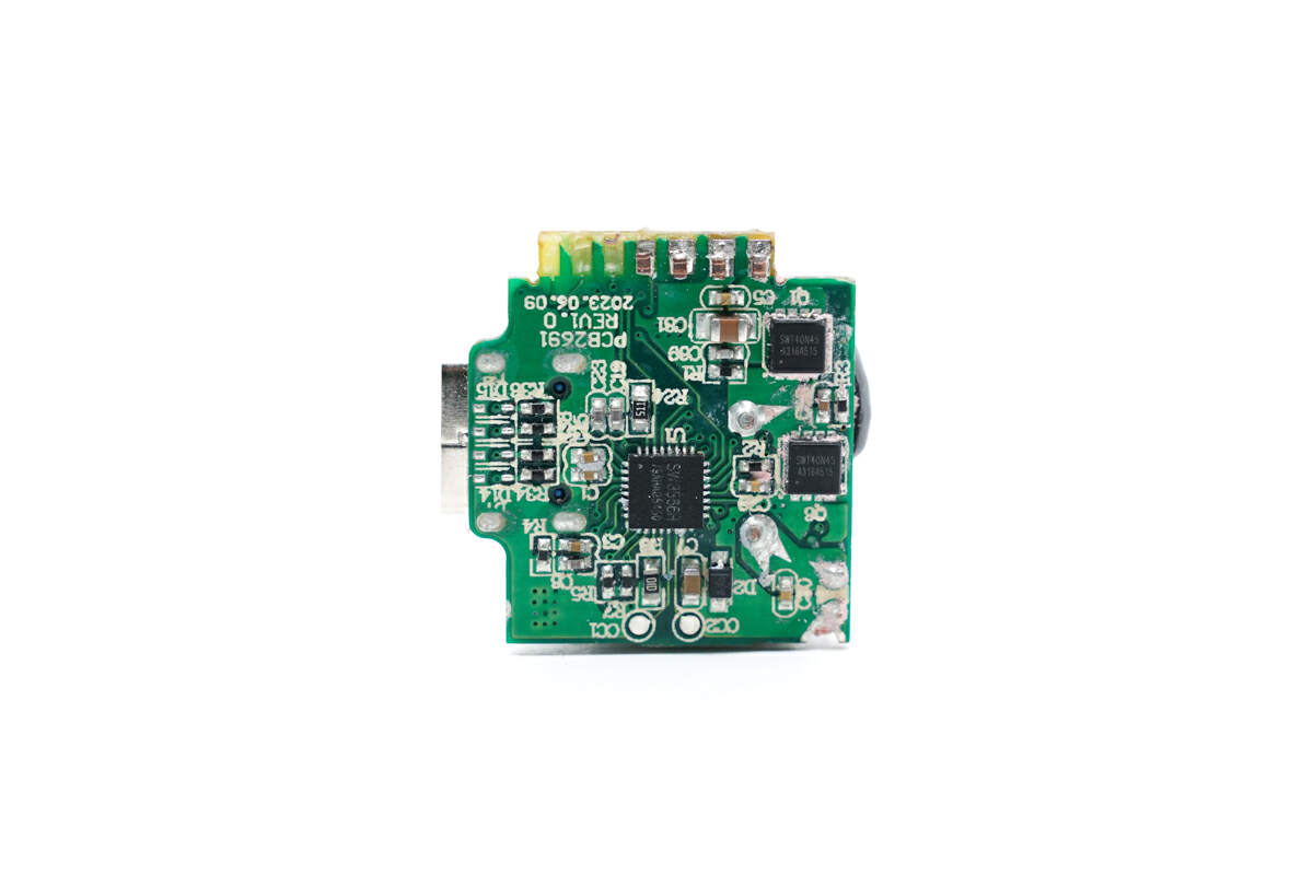
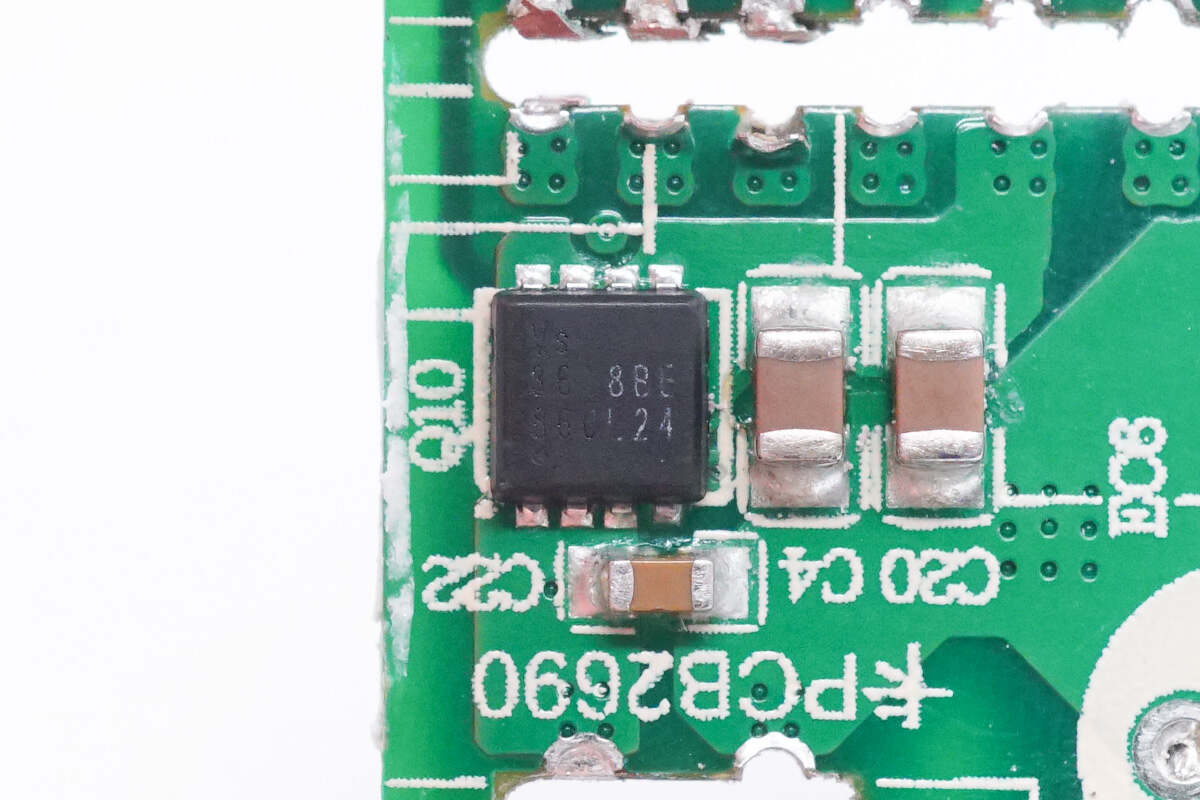
The back has buck controller and MOSFET.
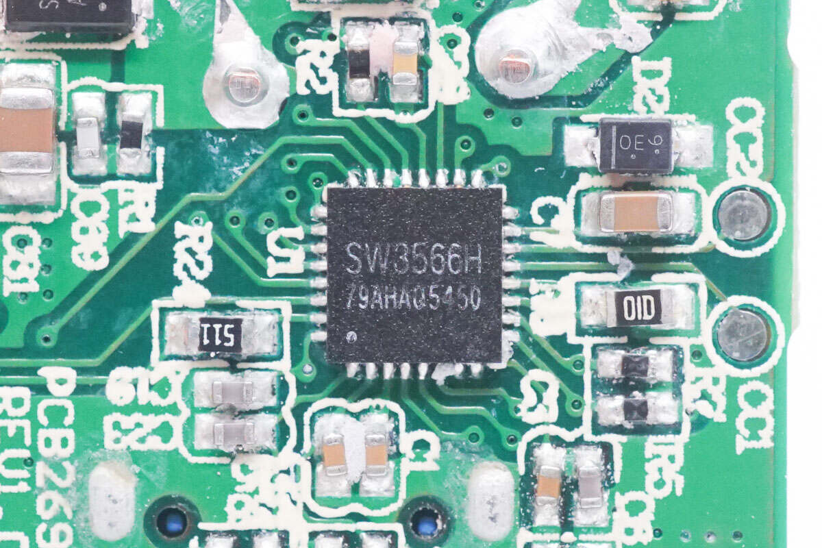
The buck controller of USB-C2 and USB-A is from iSmartWare, and it is a highly integrated multi-protocol dual-port charging SoCthat supports charging of any USB-C and USB-A ports. It supports output of 20V 7A and 28V 5A. It supports PD3.1, QC, SCP, UFCS, and other fast-charging protocols. Model is SW3566H.
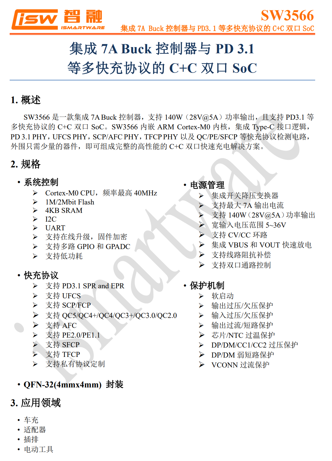
Here is all the information about the iSmartWare SW3566H.
It integrates CC and CV modes. It supports PWM and PFM working modes and adopts QFN4 x 4-32 package.
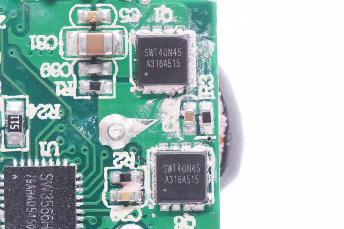
The MOSFET used for secondary synchronous buck circuit is from iSmartWare. Model is SWT40N45.
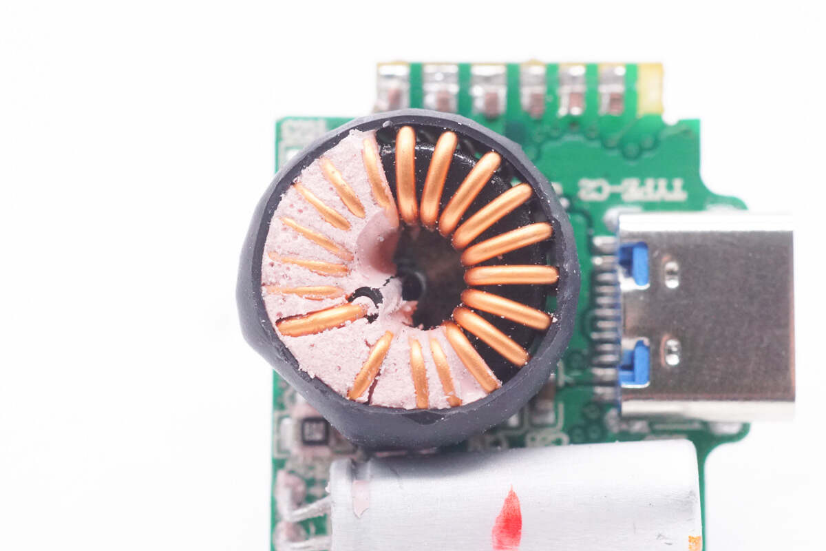
The buck inductor is wound with magnet wires and insulated by heat-shrinkable tubing.
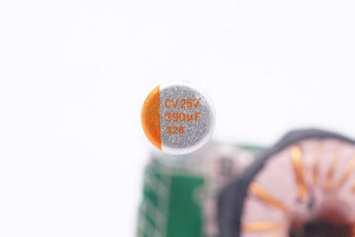
The specs of this solid capacitor for output filtering is 25V 390μF.
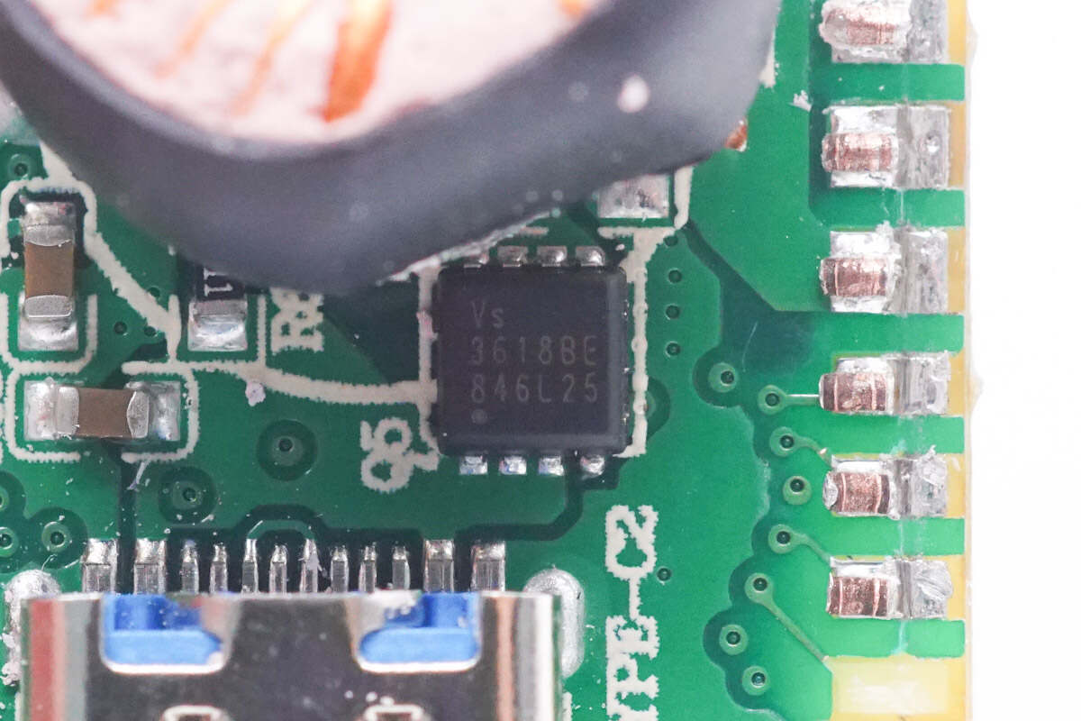
The VBUS MOSFET for USB-C2 is from VGSEMI. Model is VS3618BE. It is the same as that of the USB-C1.
The USB-C2 socket also has a blue plastic sheet.
The VBUS MOSFET for USB-A is also from VGSEMI. Model is VS3618BE.
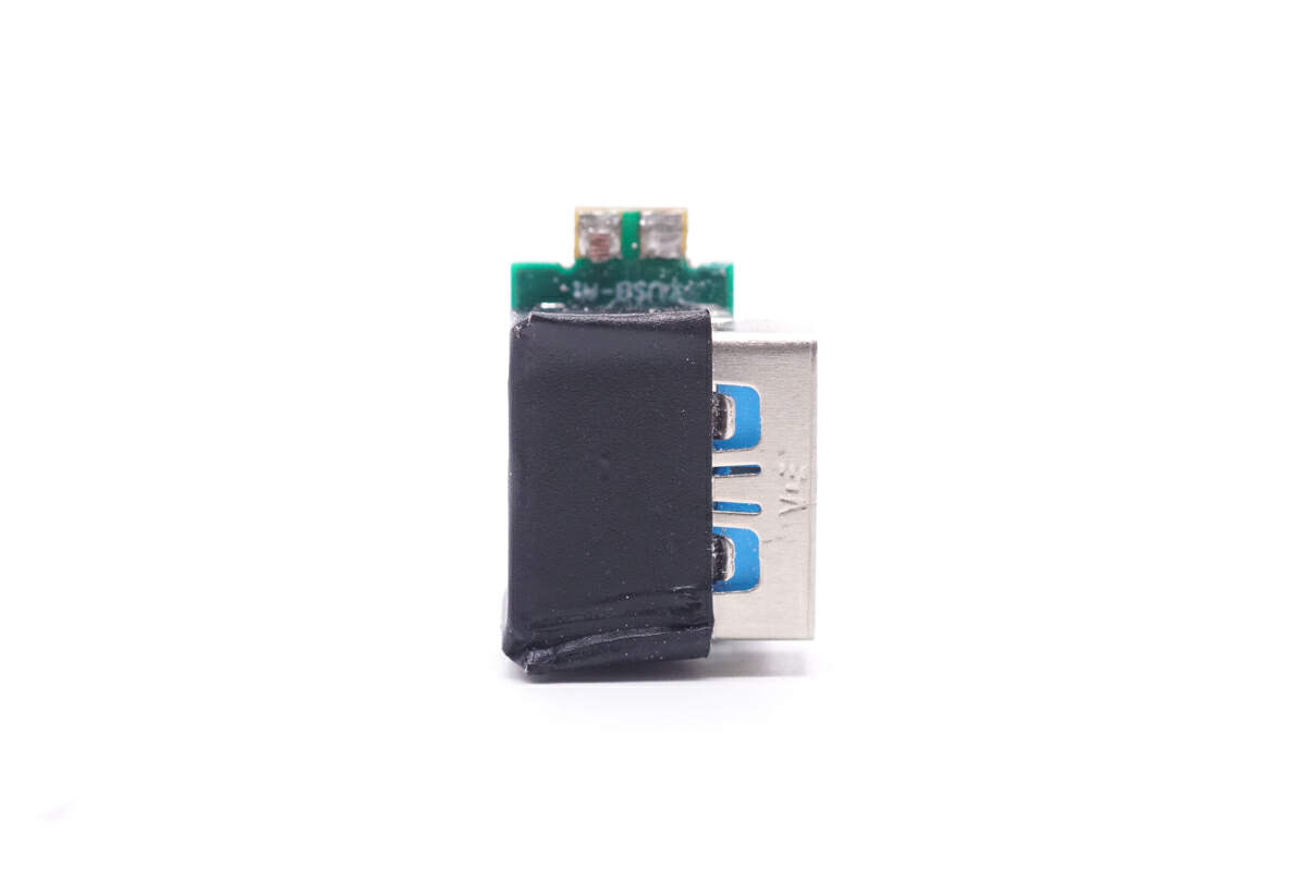
The USB-A socket is insulated by black tape.
The USB-A also has a blue plastic sheet.
Well, those are all components of the ANKER 65W 3-in-1 GaN charger.
Summary of ChargerLAB
The ANKER 65W 3-in-1 GaN charger has a fire-retardant rounded case. The foldable prongs it comes with make it easy to carry. Both USB-C ports can support up to 65W and the USB-A port can also support fast charging.
After taking it apart, we found it adopts two independent buck circuits to achieve three-port fast charging and automatic power distribution. It also has a fixed output voltage. The PCBA module and the gaps are filled with pounding compound for heat dissipation. It is commendable that it can achieve a charging power of 65W in such a small size, and it even has three ports.
Related Articles:
1. Teardown of Anker 150W GaNPrime 747 Charger (A2340)
2. Teardown of Anker 3-in-1 MagSafe Charging Cube (Y1811)
3. Teardown of Anker 30W USB-C GaN 511 Charger (Nano 3)