Introduction
ChargerLAB previously introduced USB-C Hubs for the iPhone 15 series. This time, we got a 6-in-1 USB-C hub from Anker. It has two USB-A ports, two USB-C ports, an HDMI port, and an RJ45 port. It can support simultaneous expansion of 5 ports. The HDMI port supports 4K 30Hz output.
And next, let's take it apart to see the internal components of this 6-in-1 USB-C hub.
Product Appearance
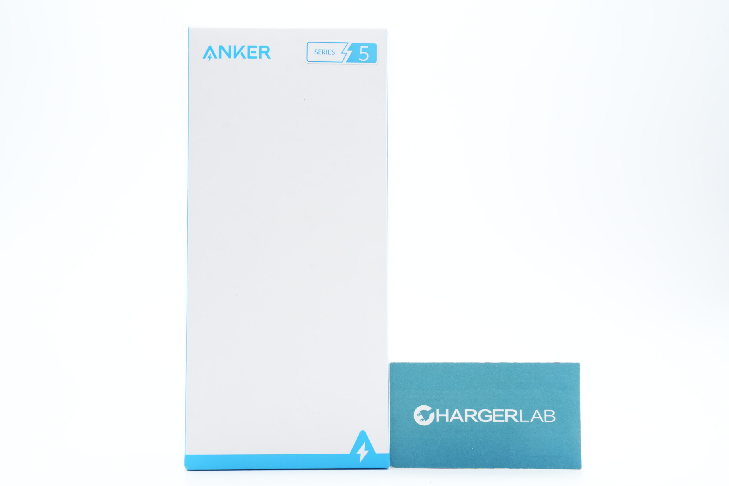
The packaging box is simple in style, with the Anker printed on the front.
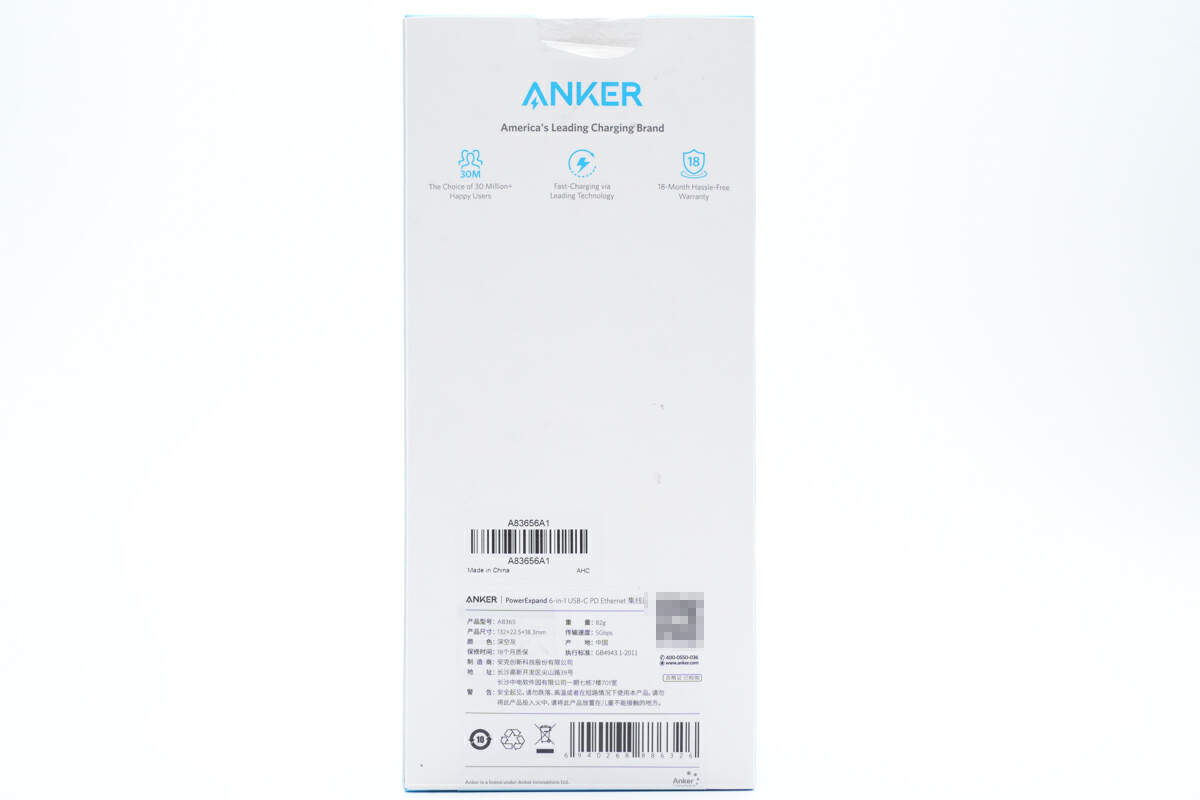
All specs info are on the back of the box.
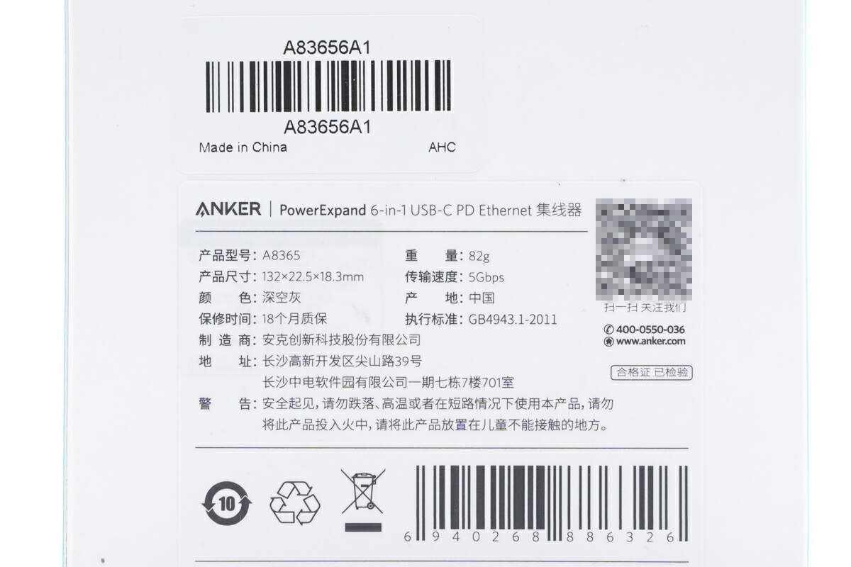
Model is A8365. It has a transmission speed of 5Gbps.
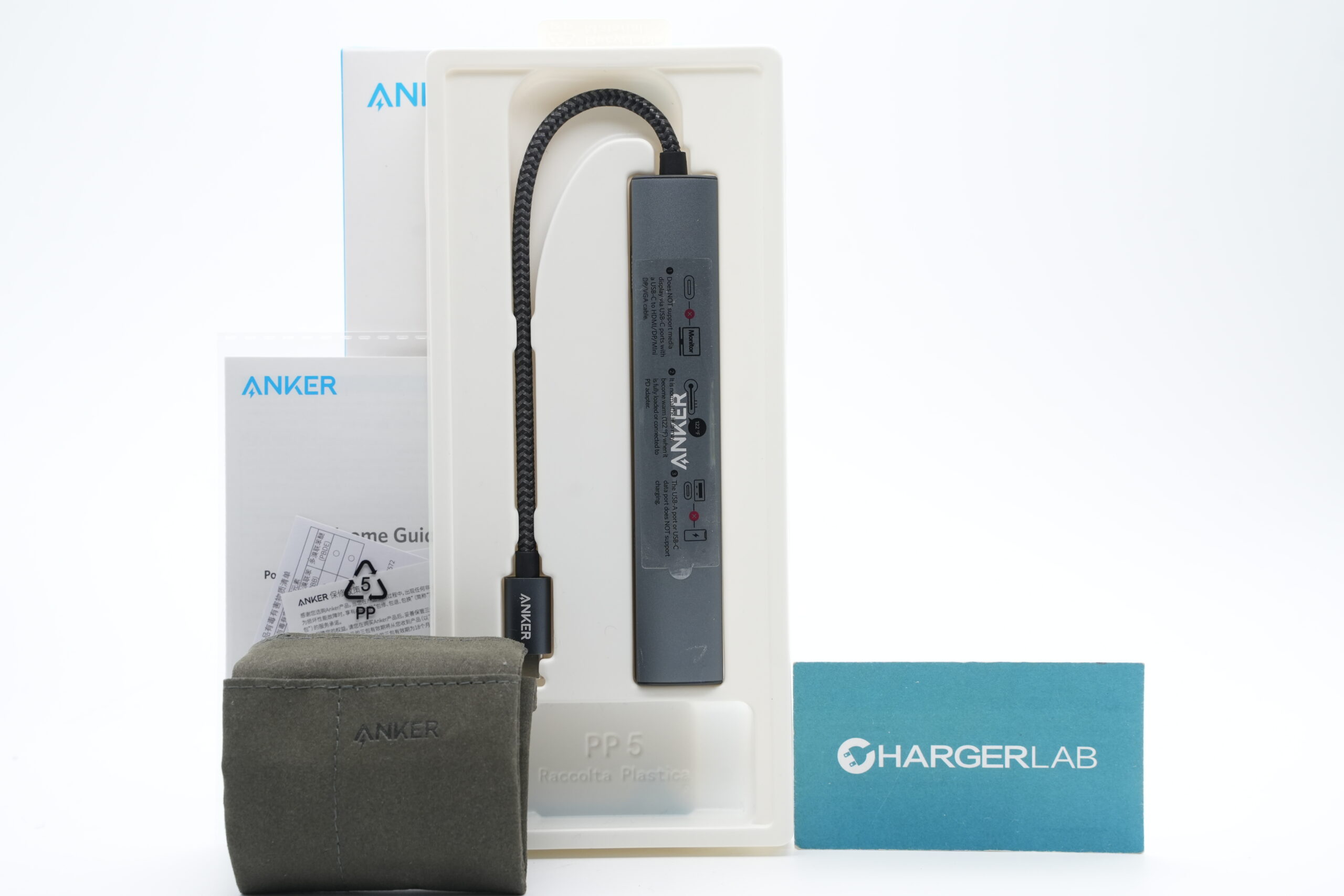
The package included the hub itself, storage bag, and some documents.
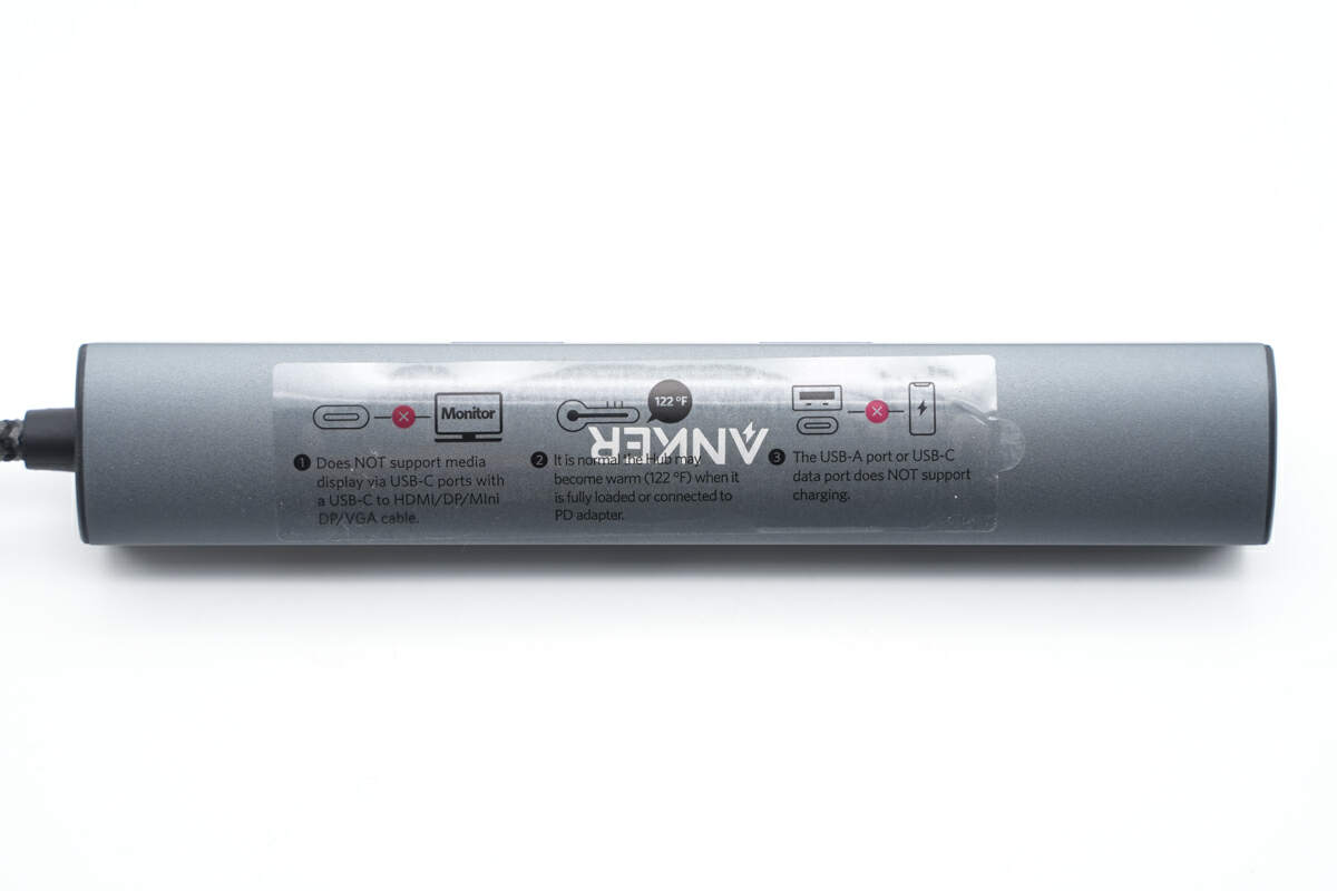
There are tips printed on its plastic film: Does NOT support media display via USB-C ports; The hub may become warm (122 ℉) when it is fully loaded; The USB-A port or USB-C data does NOT support charging.
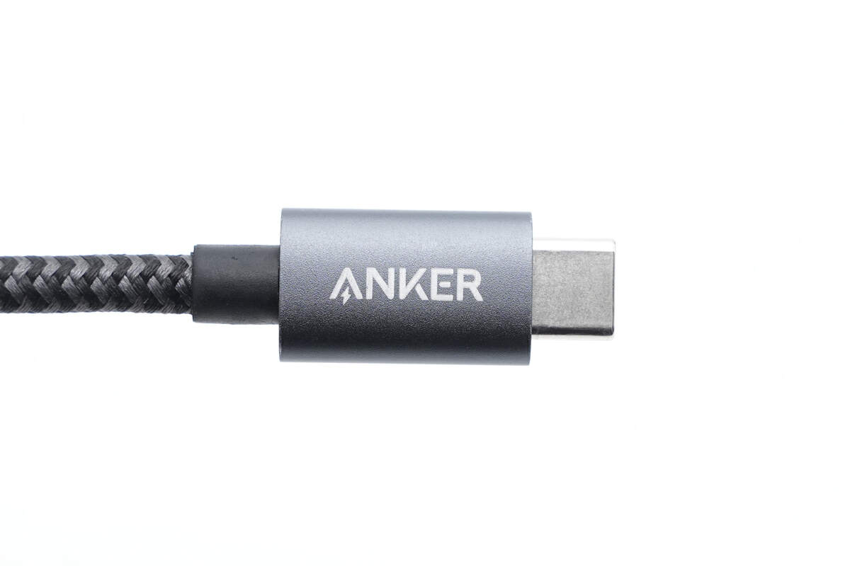
There is an ANKER logo printed on the USB-C connecter.
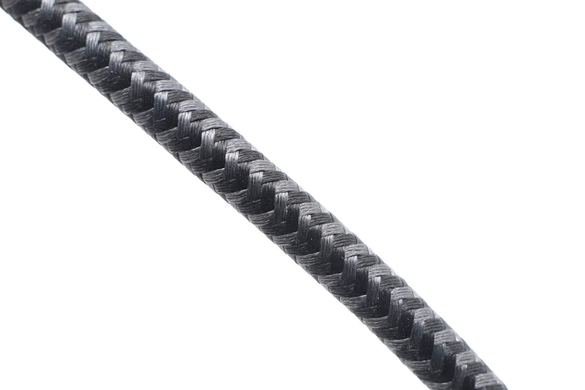
The cable adopts a braided design.
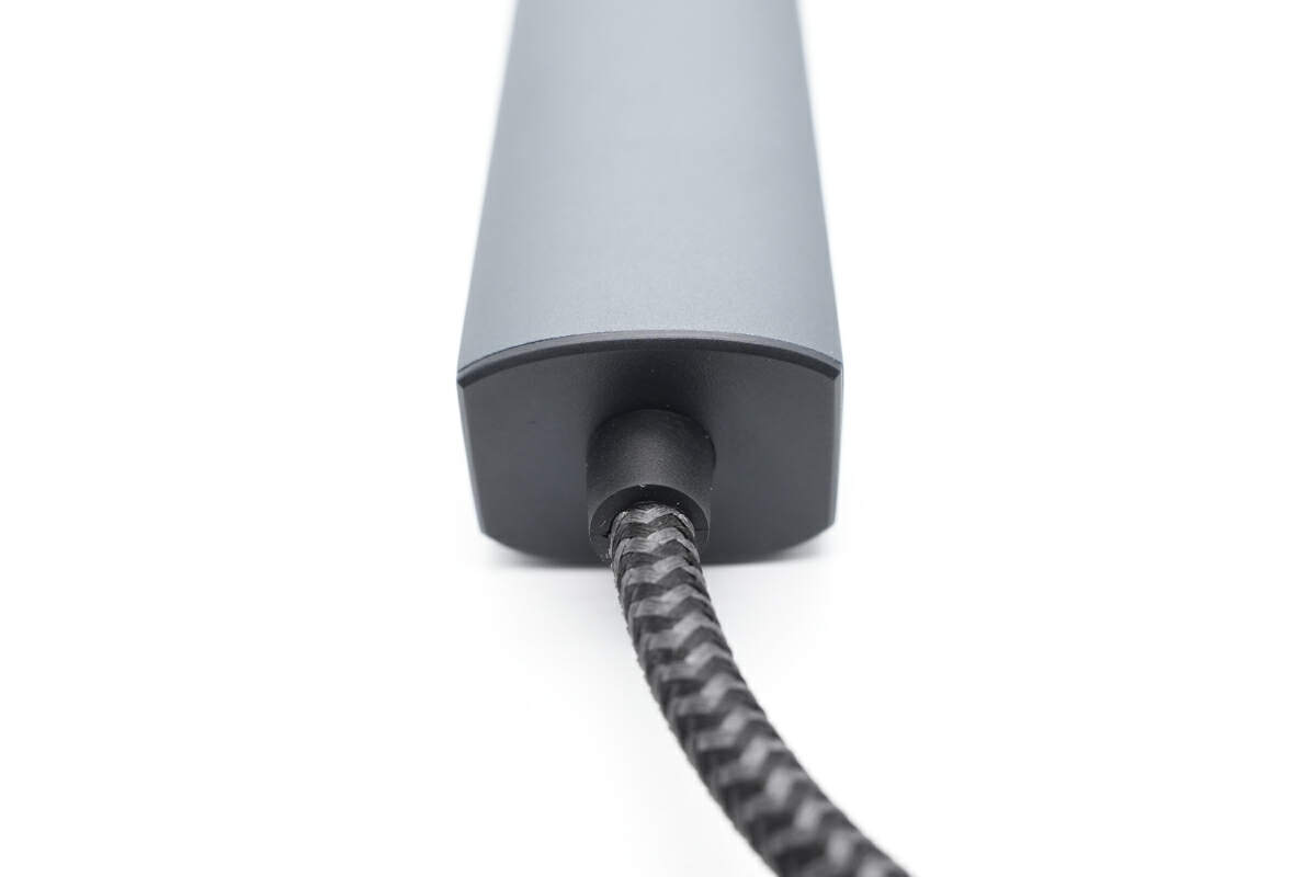
The thickened plastic is for anti-bending protection.
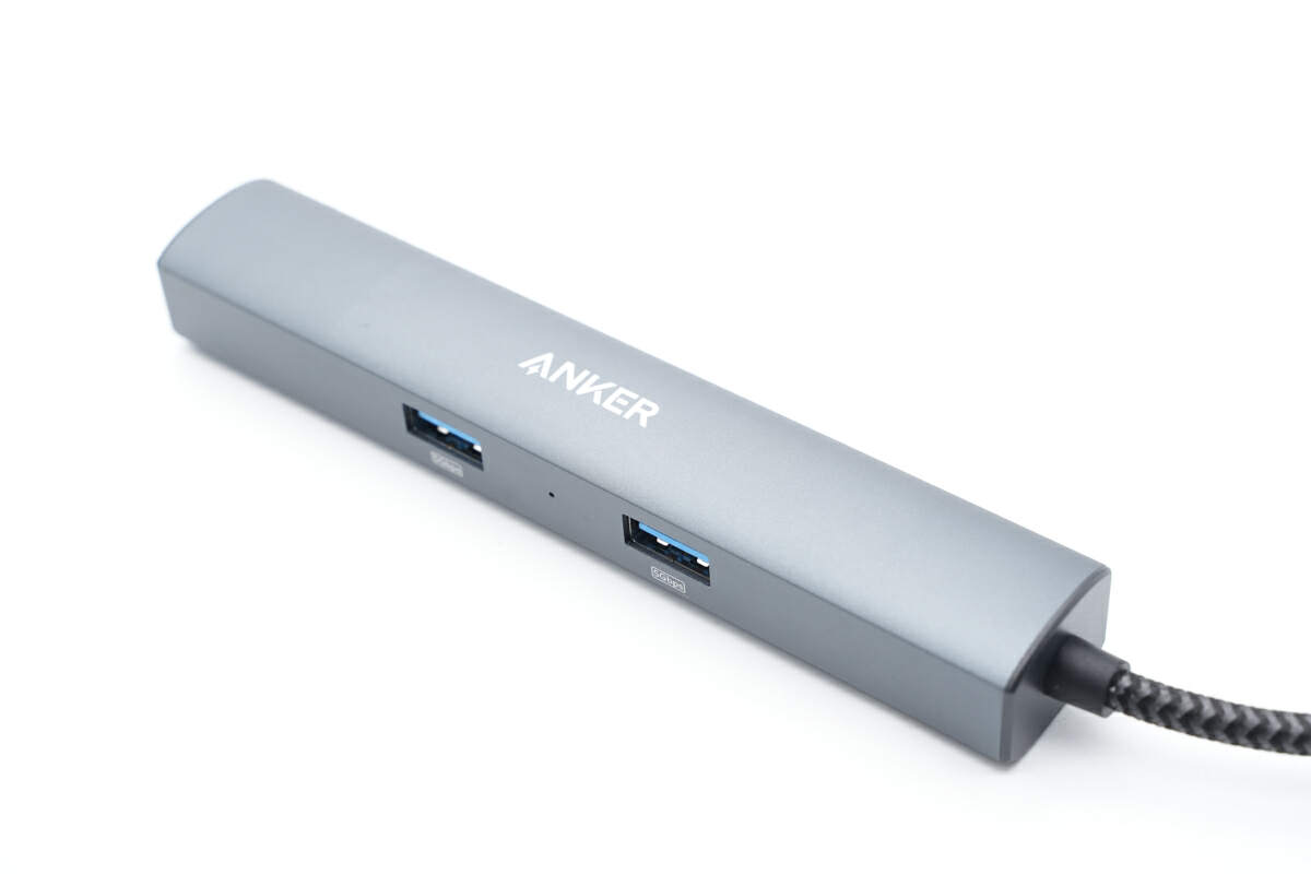
It's painted silver gray metallic.
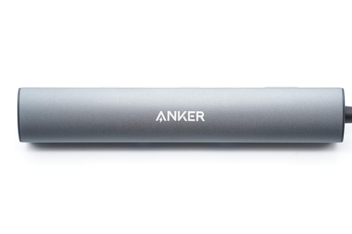
There is a Anker logo on the front.
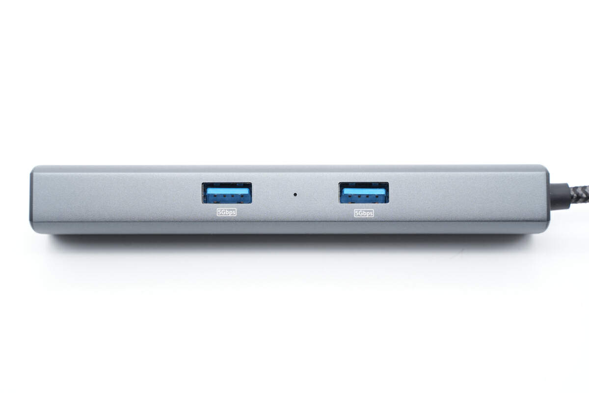
Both of the USB-A ports have a transmission speed of 5Gbps.
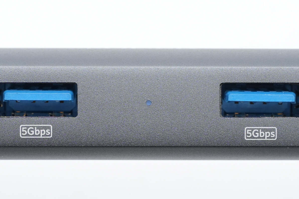
A blue indicator light is in the middle, it will light up when powered on.
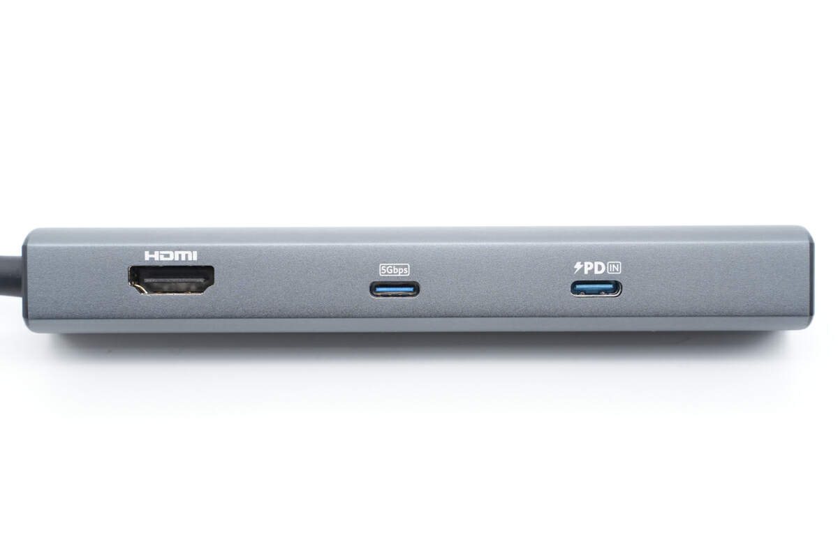
The other side has an HDMI and two USB-C ports.
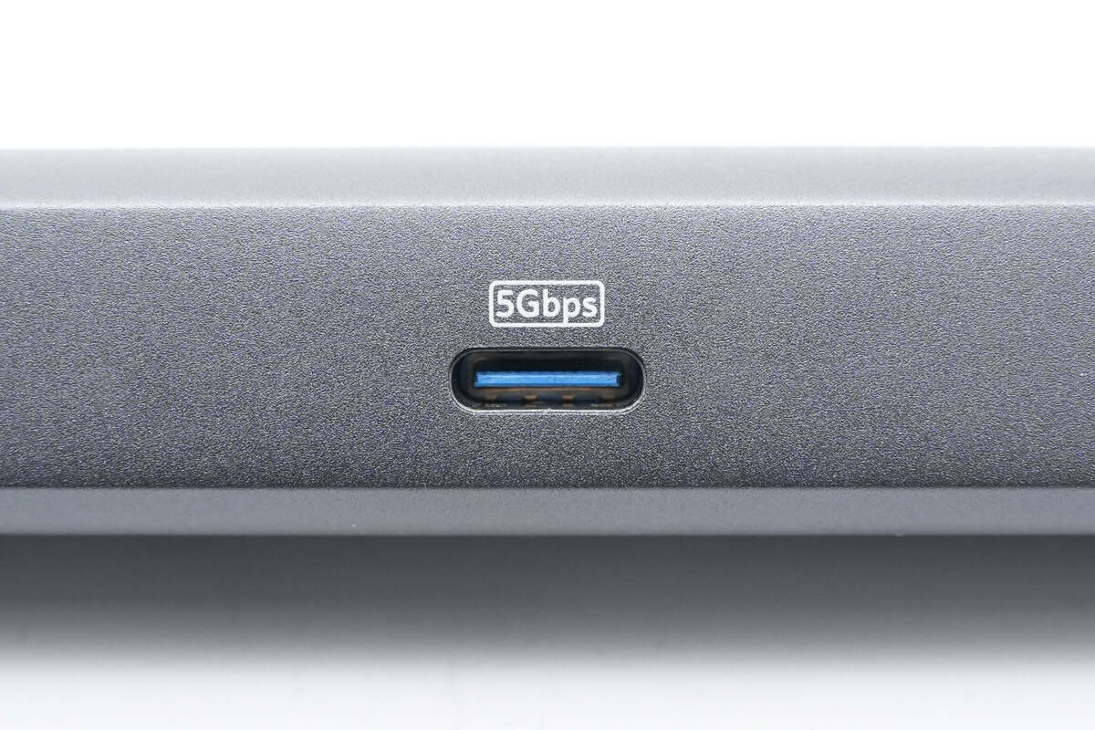
One of the USB-C ports has a transmission speed of 5Gbps.
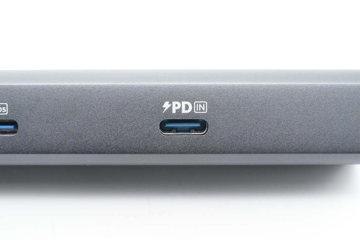
The other USB-C port can support charging power of PD 65W. It can charge laptop while using.
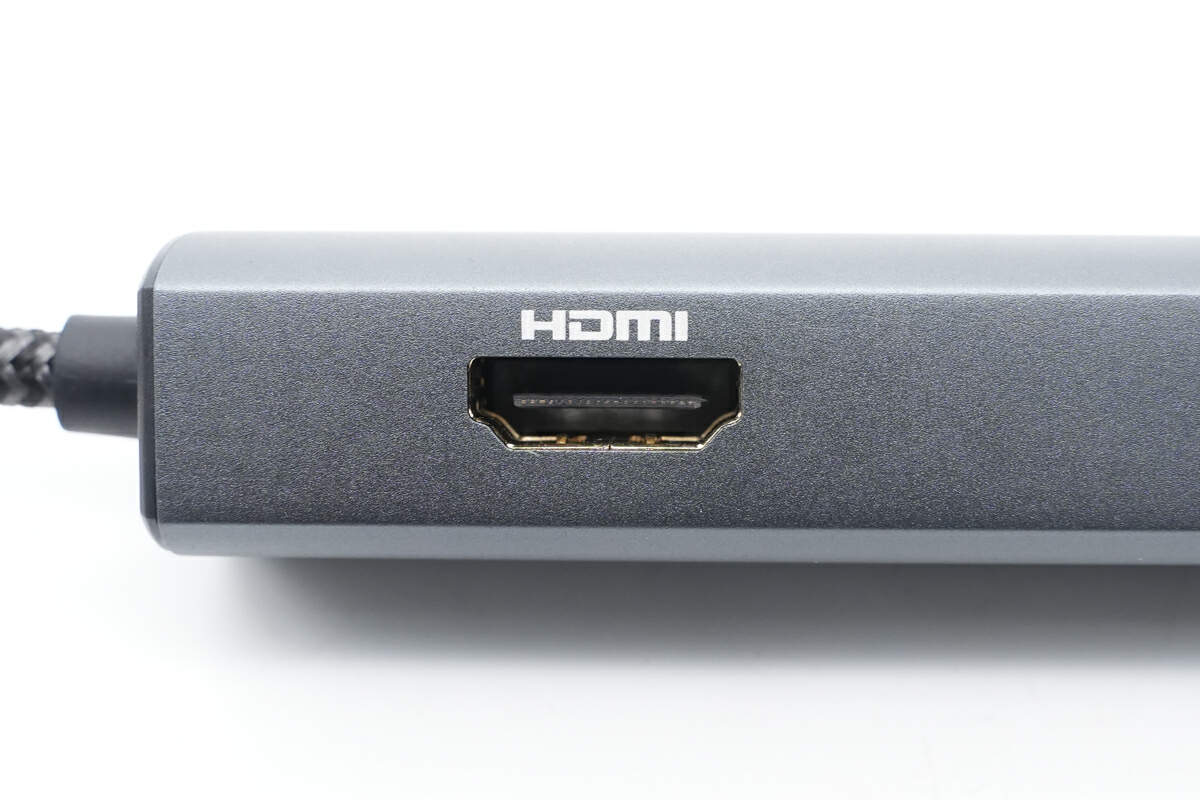
The HDMI port can support media display of 4K.
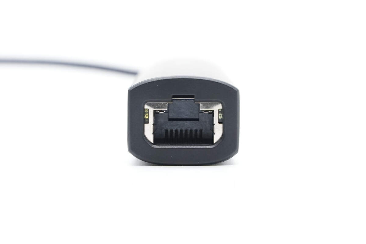
There is a network port at the end.
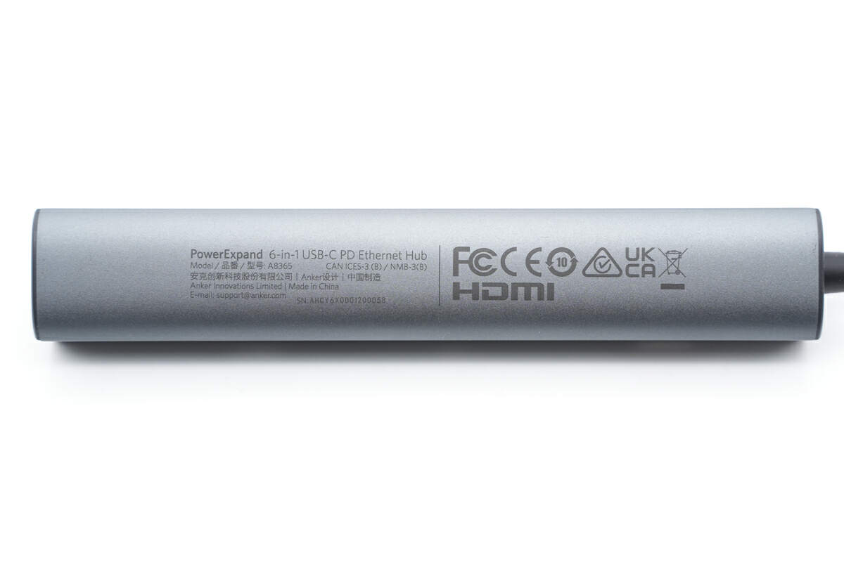
It has passed FCC, CE, and other certifications.
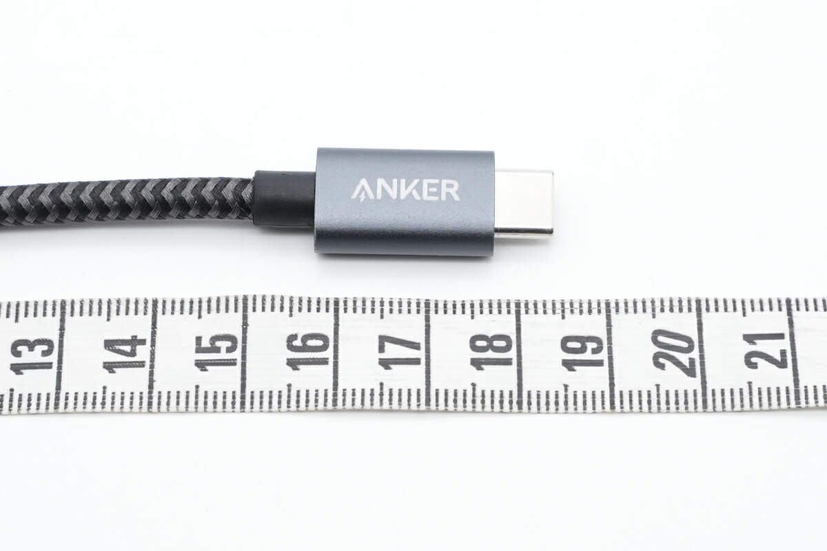
The length of the cable is about 19 cm (7.48 inches).
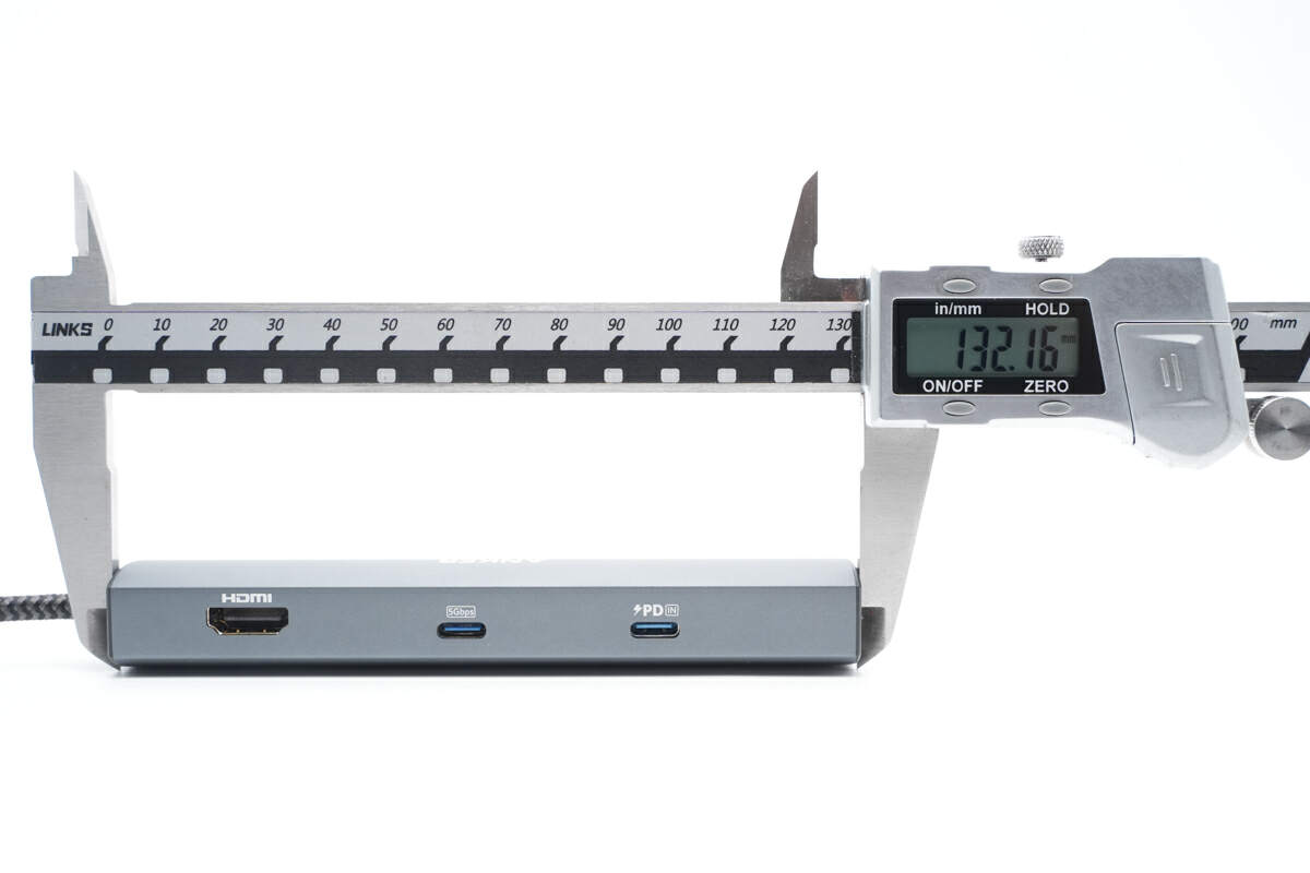
The length of the hub is about 132 mm (5.2 inches).
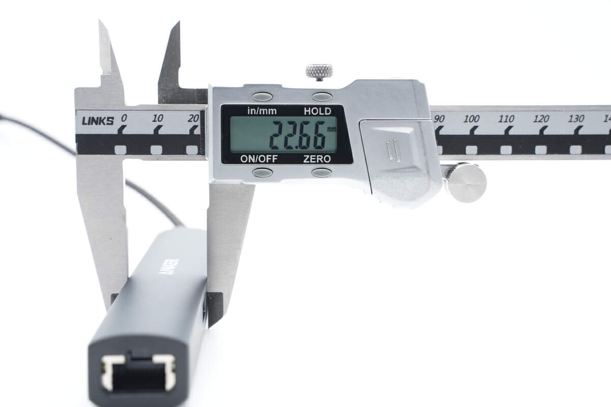
The width is about 23 mm (0.91 inches).
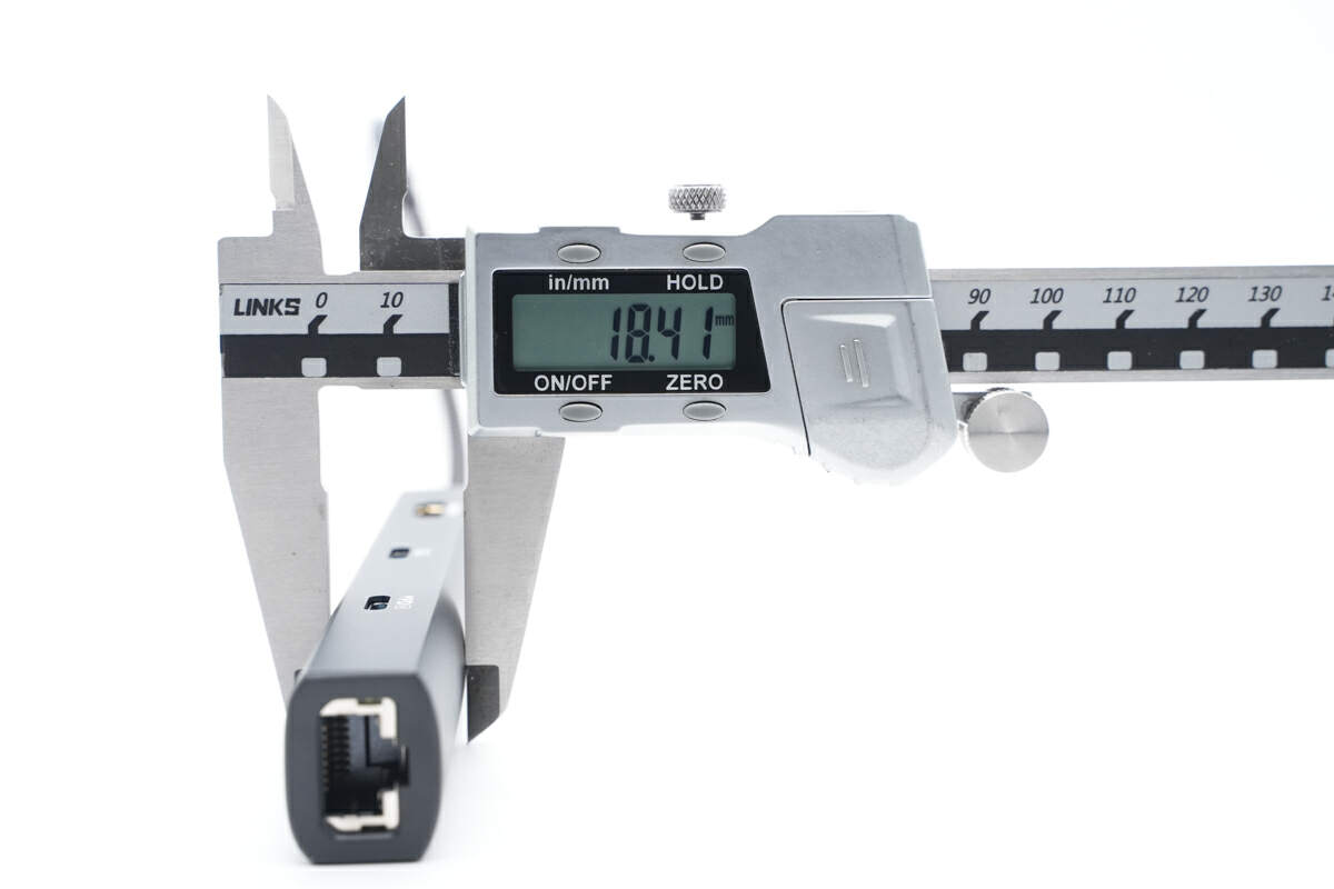
The thickness is about 18 mm (0.71 inches).
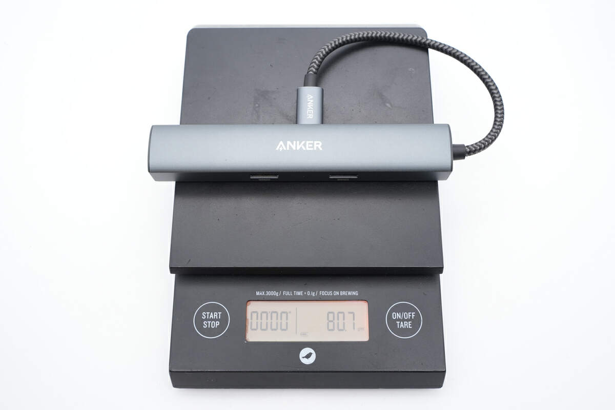
And the weight is about 81 g (2.86 oz).
Teardown
Now, let's start to take it apart.
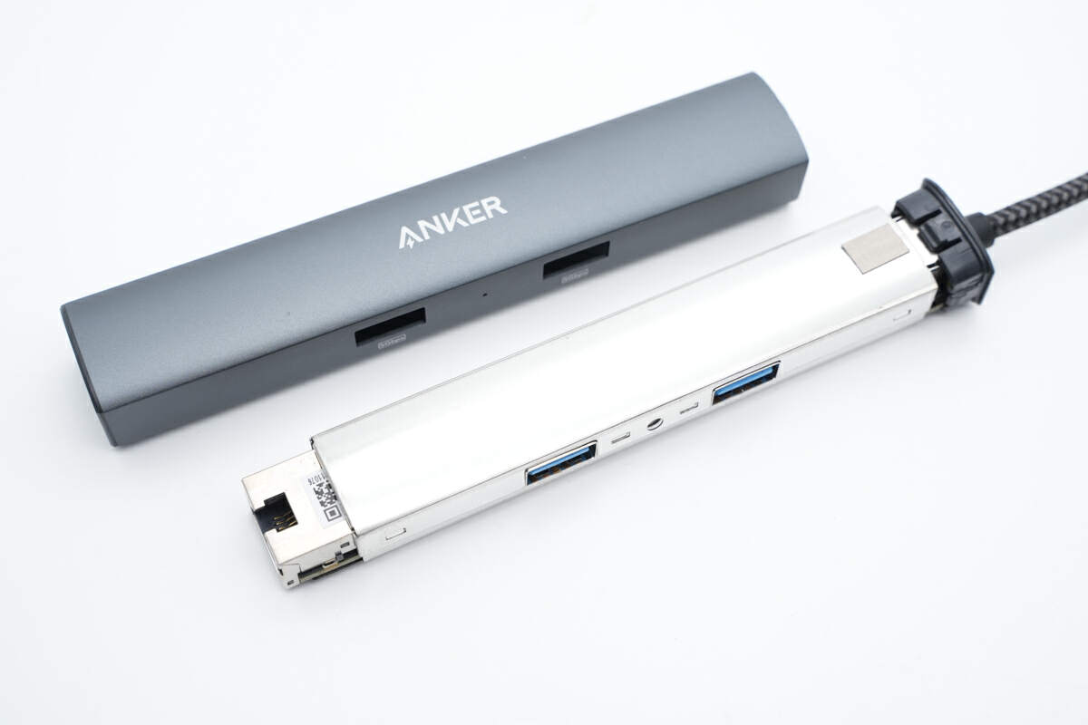
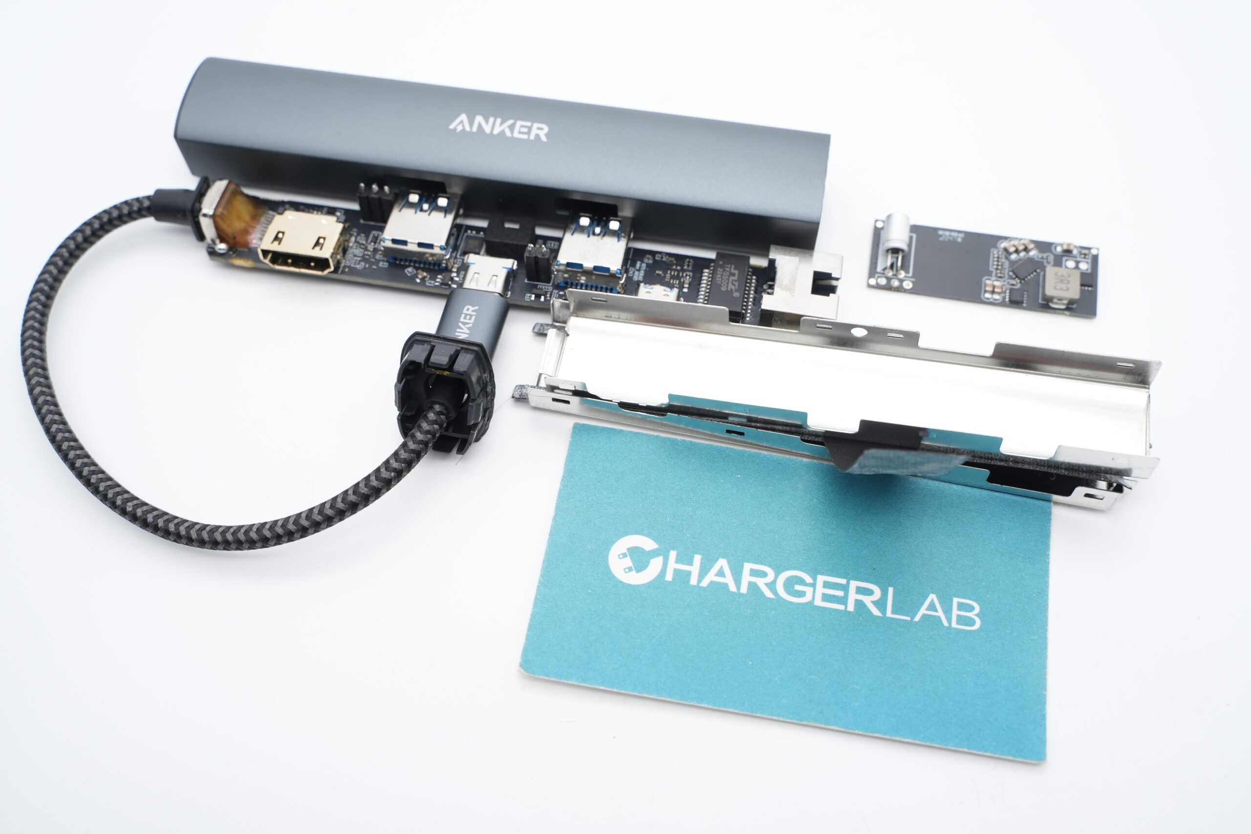
Remove the case and take out the PCBA module.
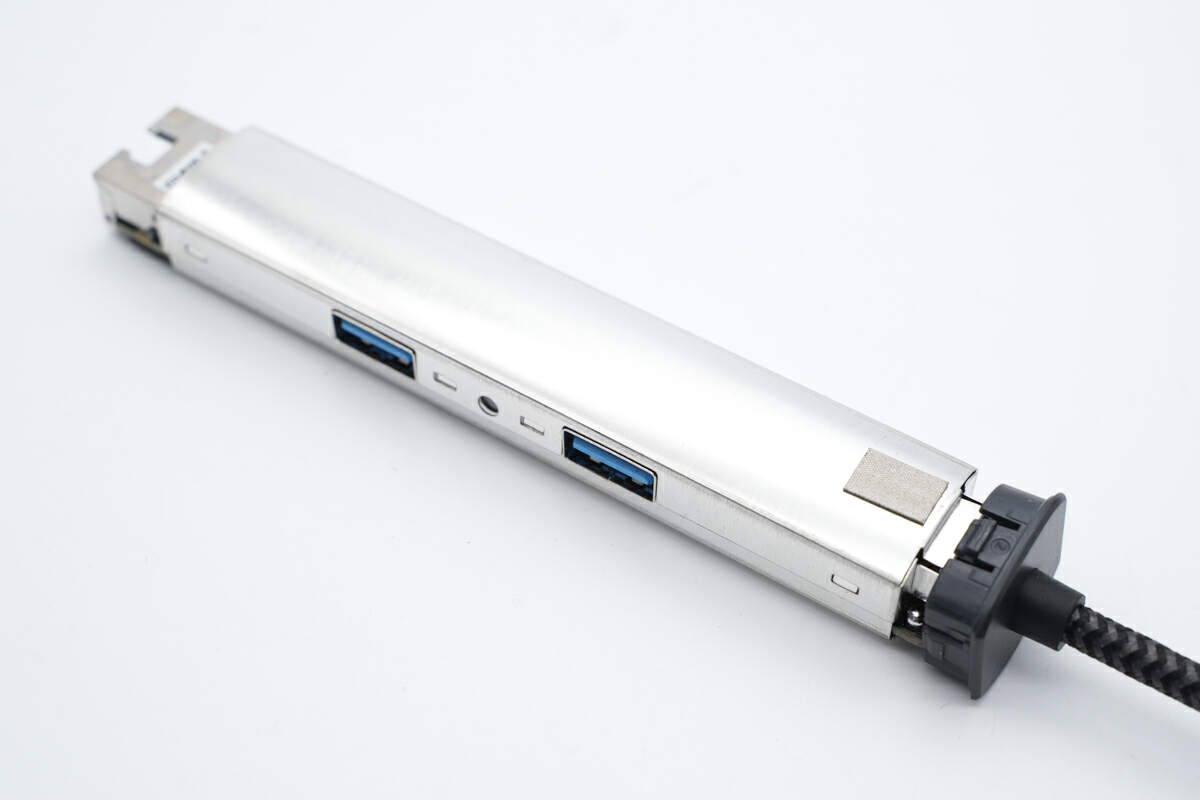
The PCBA module has an aluminum alloy case and is pasted with conductive cloth for grounding.
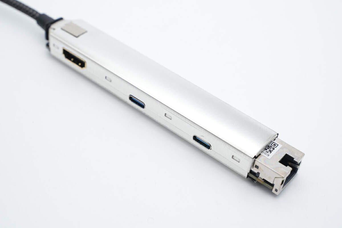
The case is fixed with snaps.
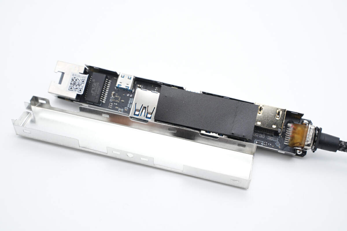
Remove the aluminum alloy case, the PCBA module is insulated by mylar sheets.
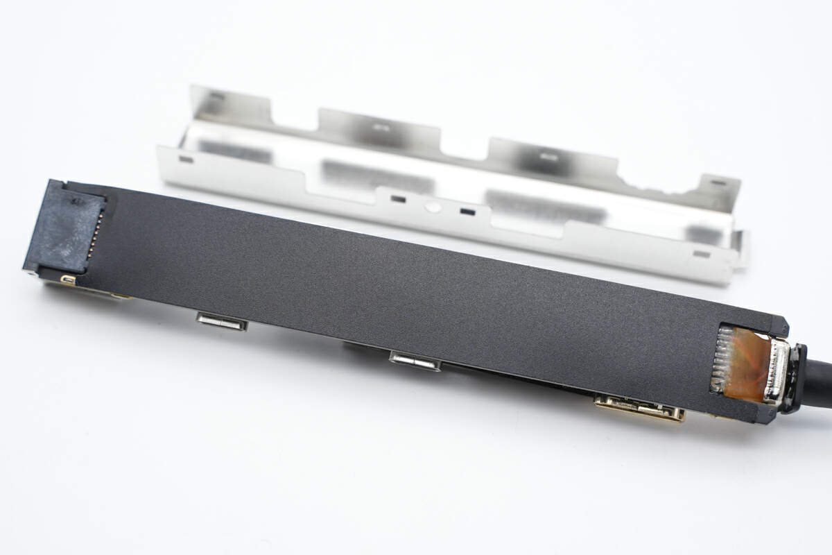
So as the back of the PCBA module.
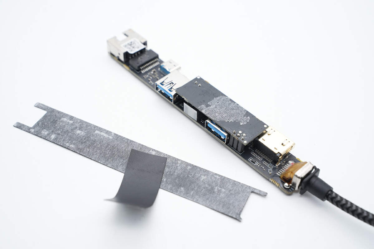
Remove the mylar sheets.
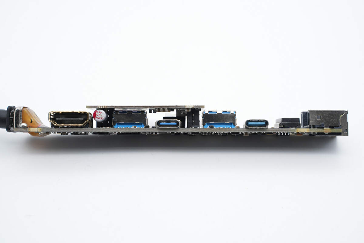
There is a small PCB soldered on the front of the PCBA module.
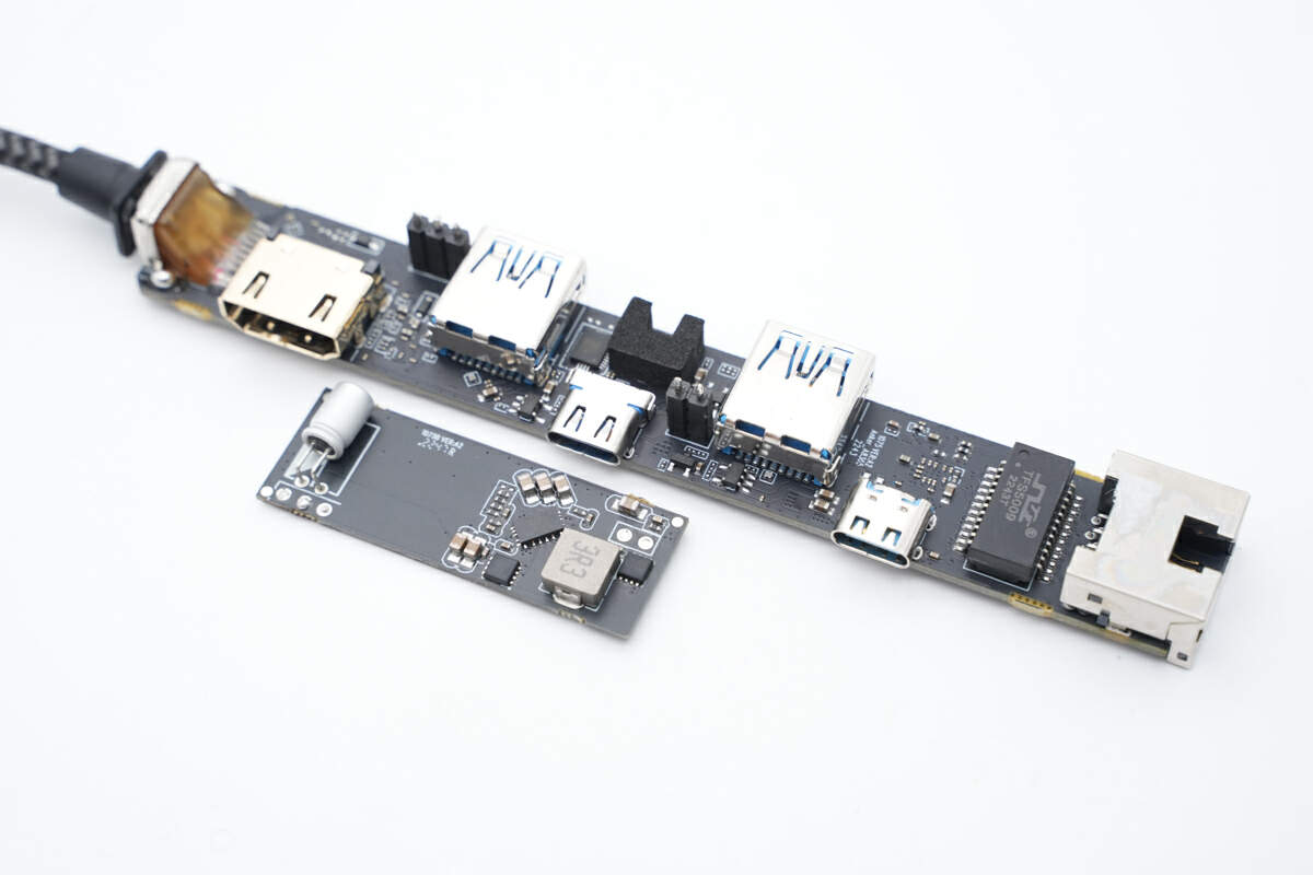
Remove the small PCB and continue to take it apart.
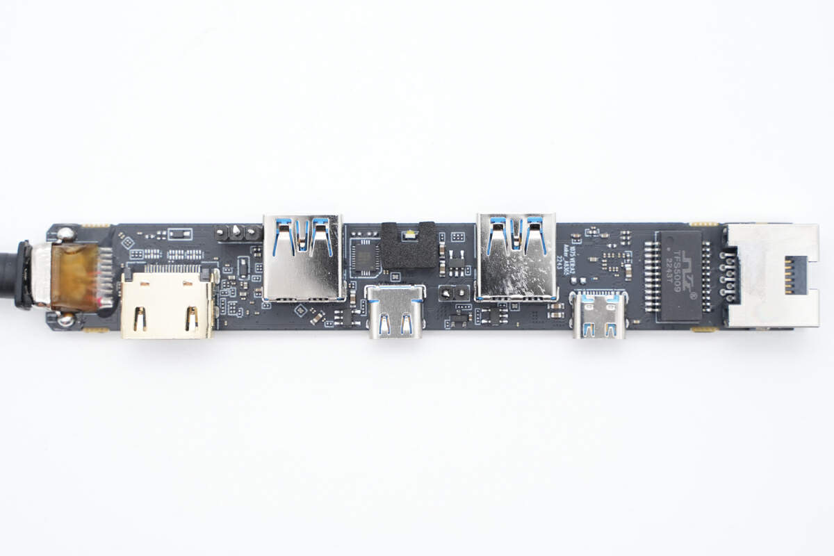
There are lots of sockets on the front.
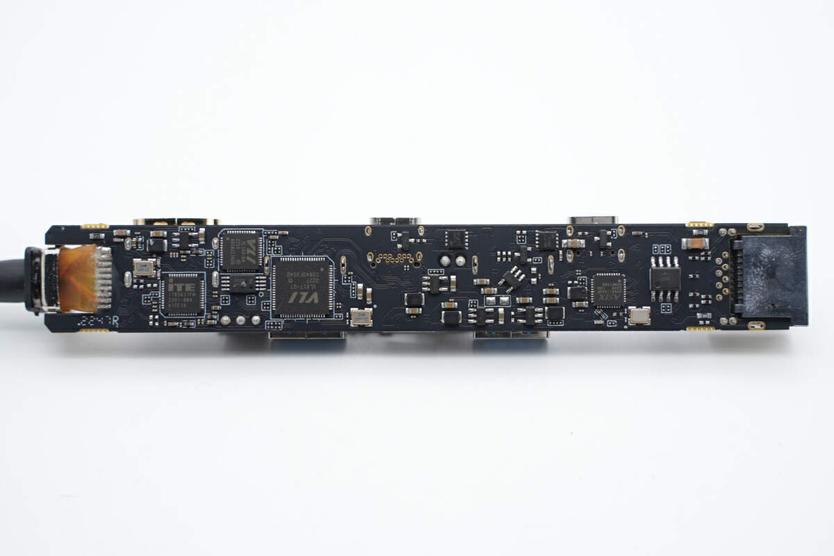
The HDMI converter, USB-C controller, USB hub chip, and Ethernet controller are on the back.
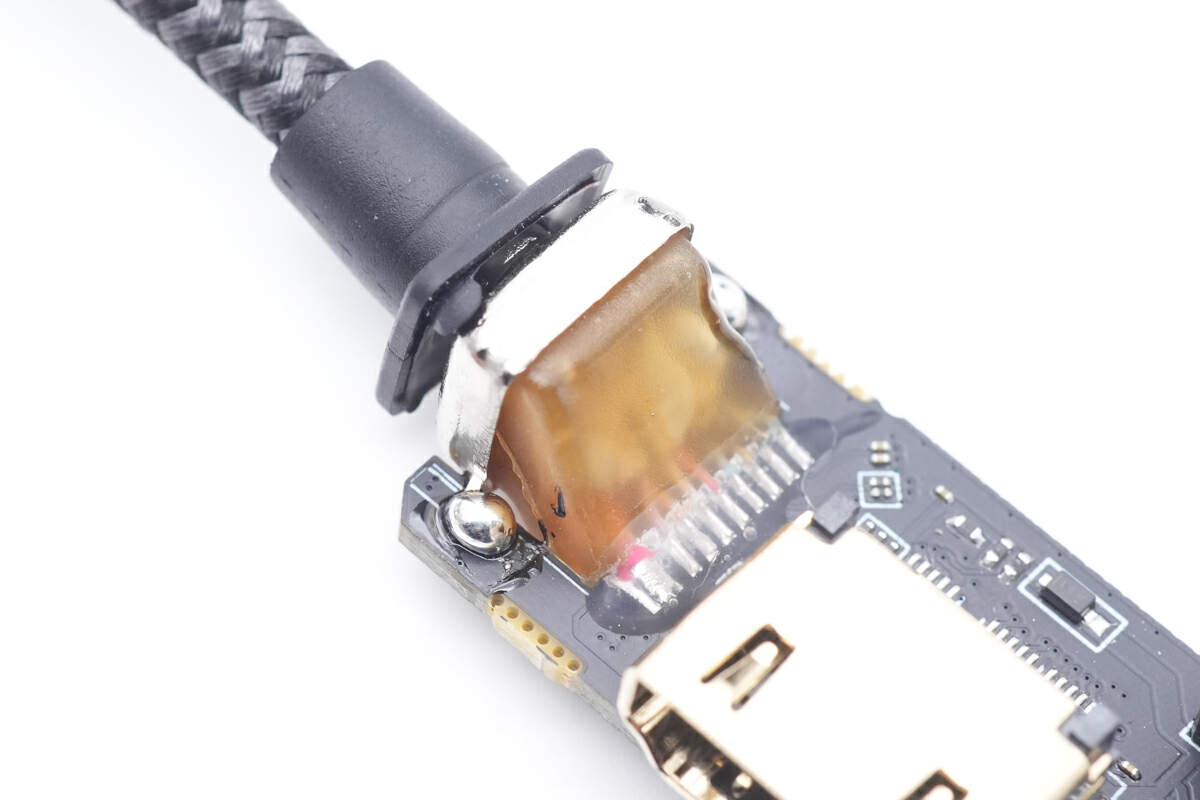
The built-in cable and its metal case are soldered on the PCBA module.
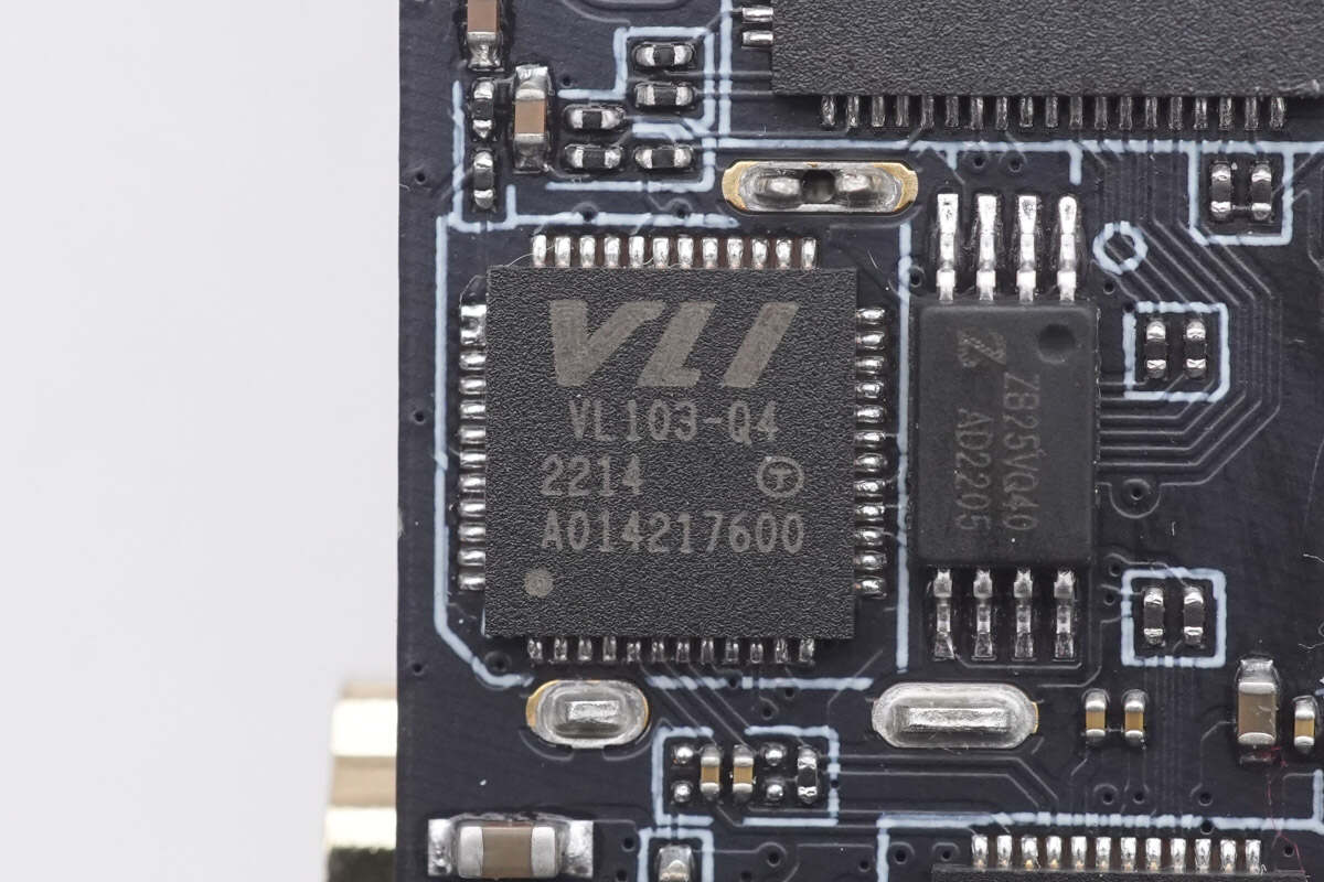
The USB-C controller is from VIA Labs, and it's a highly integrated DP converter and PD3.0 controller. It is used for USB-C video, multi-function converter. Model is VL103-Q4.
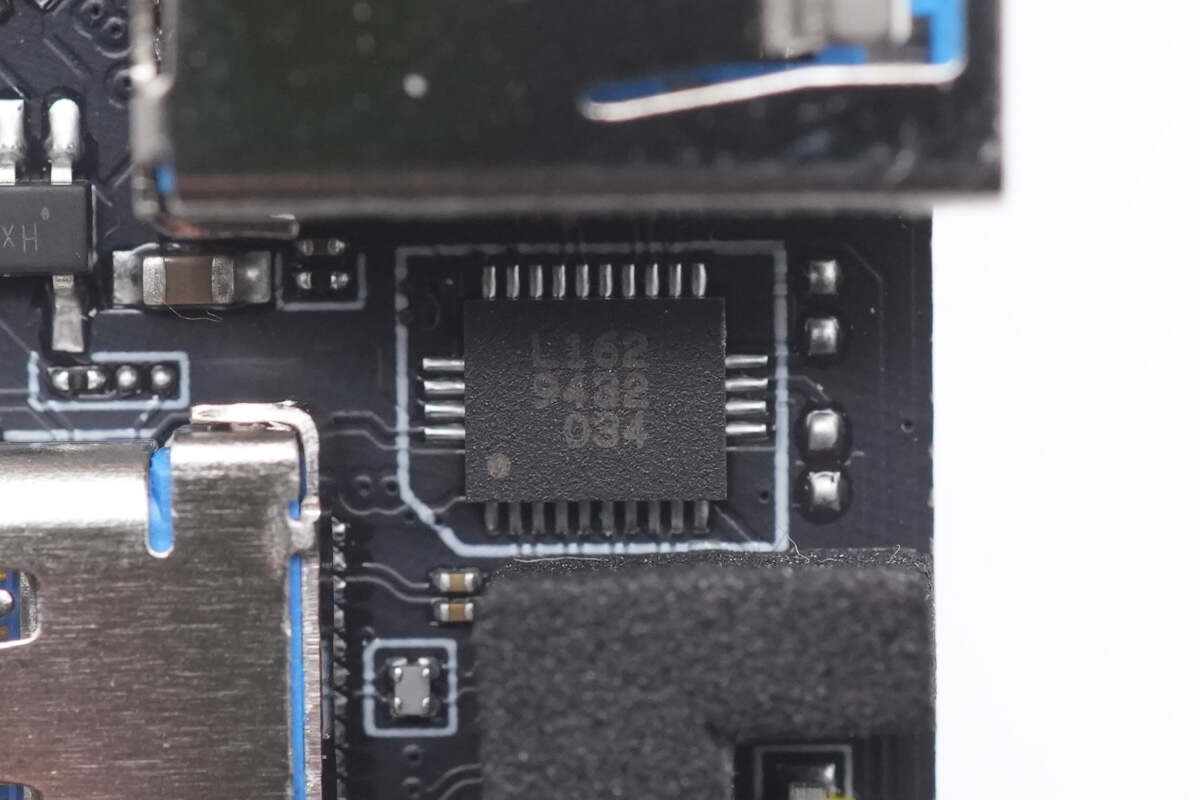
The USB-C differential channels mux switch is also from VIA Labs and used for USB-C interface reversible plug-in function. It can support USB 3.2 and adopts QFN-28 package. Model is VL162.
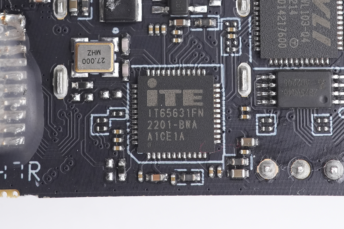
The HDMI converter is from ITE, it is a high-performance single-chip converter. It is used for DP 1.2 to HDMI 1.4 output of USB-C port, supporting 4K@30Hz, and refresh rate can be up to 120Hz. Model is IT65631.
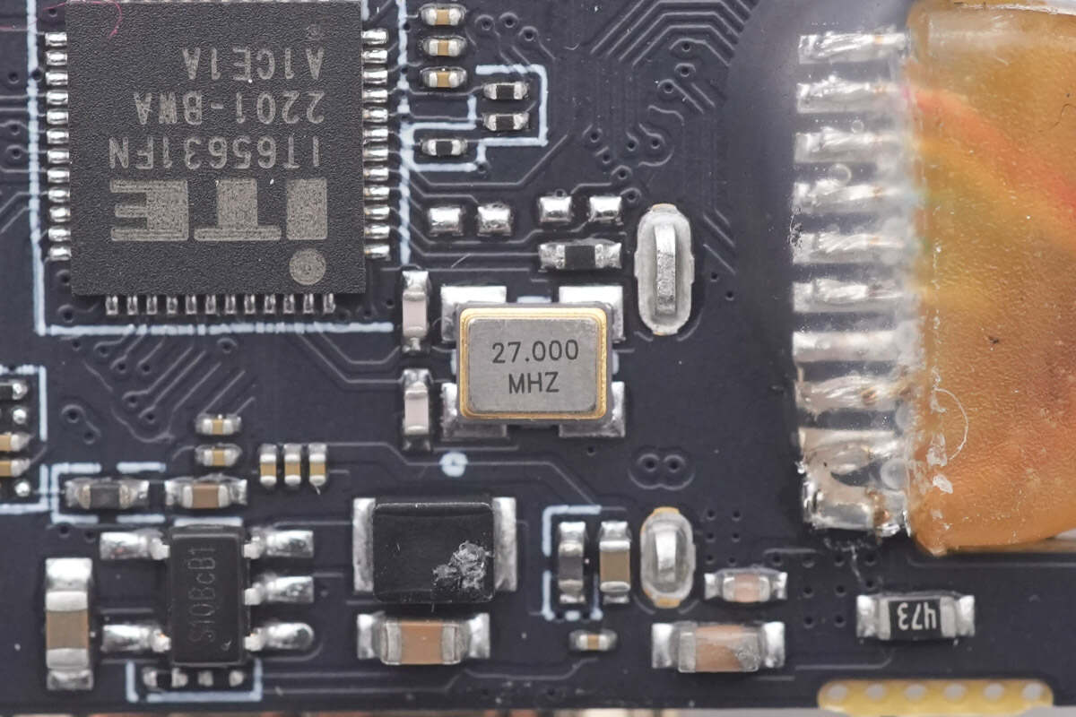
The 27.000MHz crystal oscillator is used for the HDMI converter.
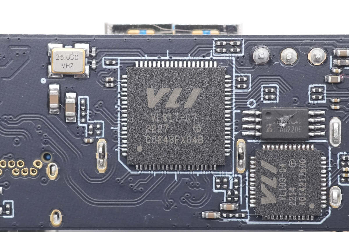
The USB hub chip is from VIA Labs, it can support up to 5Gbps. Model is VL817-Q7.
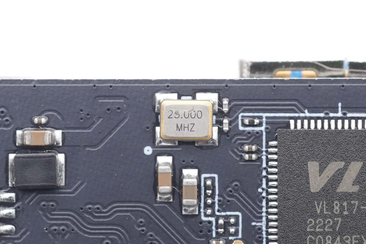
The external 25.000MHz crystal oscillator is also used for the USB hub chip.
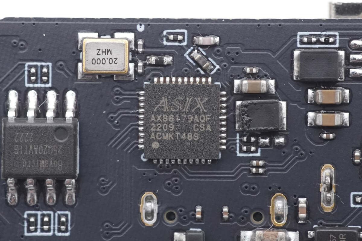
The Ethernet controller is from ASIX and it can support USB 3.2 Gen1 and integrated 10/100/1000Mbps Gigabit Ethernet PHY. Model is AX88179A.
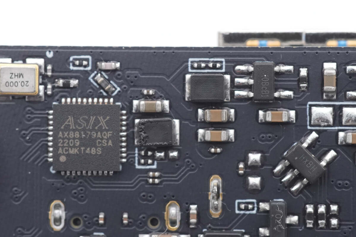
There are two SMD buck inductors around the Ethernet controller.
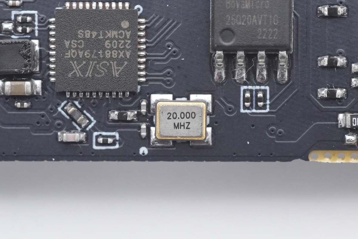
This 20.000MHz crystal oscillator is for the Ethernet controller.
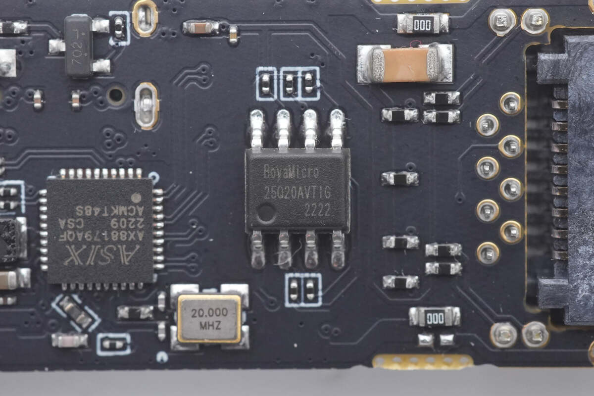
The external memory from BoyaMicro is used for the AX88179. Model is 25Q20. 256KB.
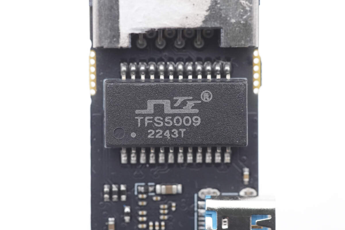
The SMD network transformer is from TF. Model is TFS5009.
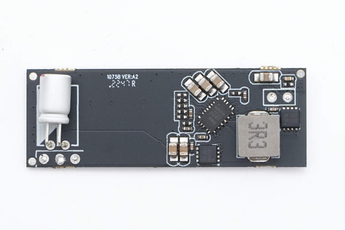
Here is the small PCB soldered on the PCBA module. There is a synchronous buck-boost circuit on it.
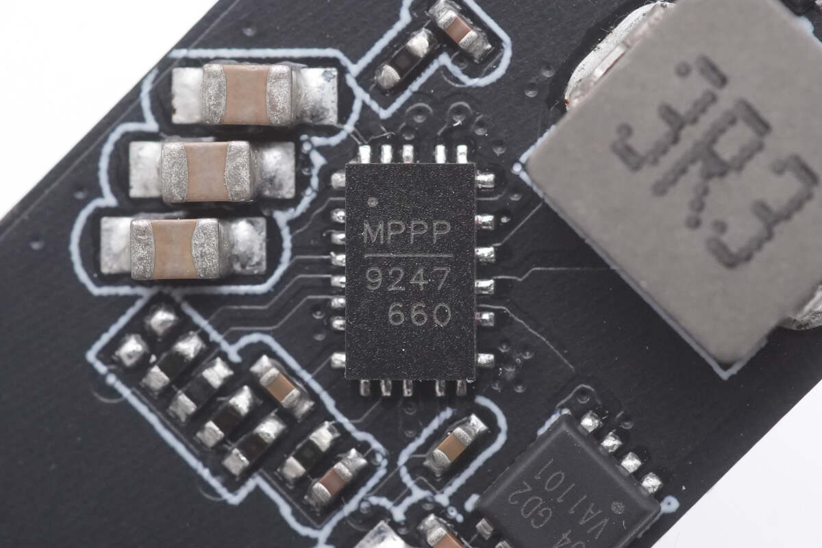
The synchronous buck-boost converter marked with 9247 is from MPS. It integrates two PMOSFETs, and two NMOSFETs to form an H-bridge.
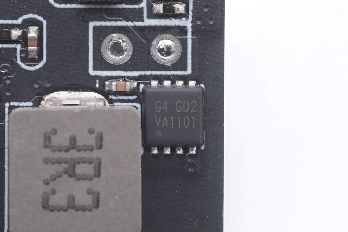
Here is the MOSFET for the converter.
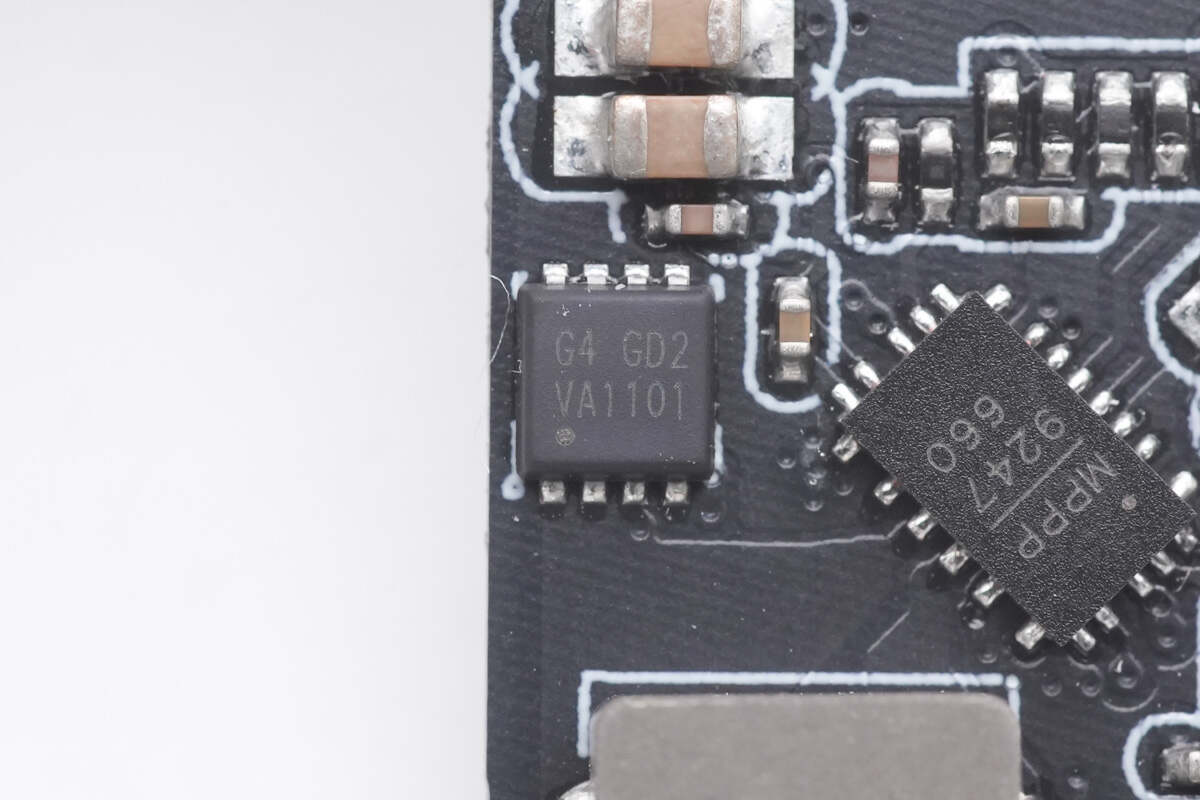
Another MOSFET has the same model.
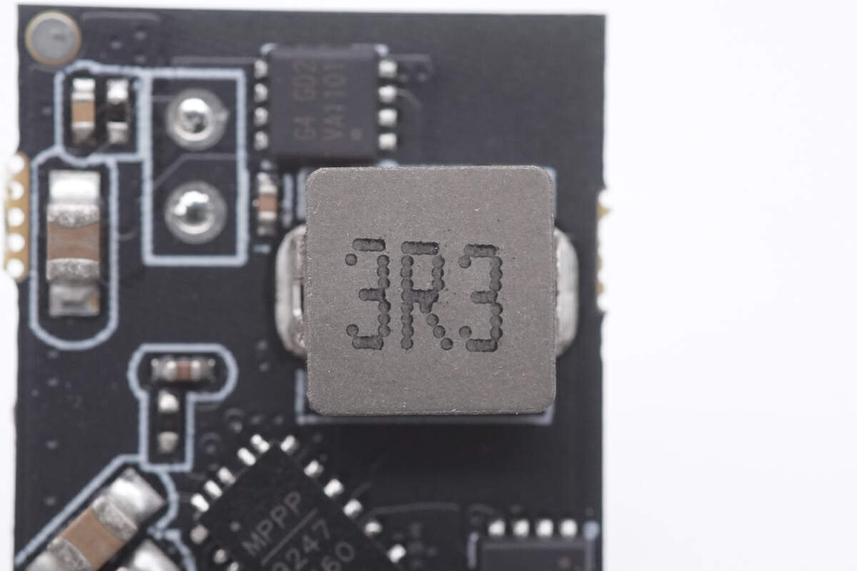
Here is the 3.3μH alloy inductor.
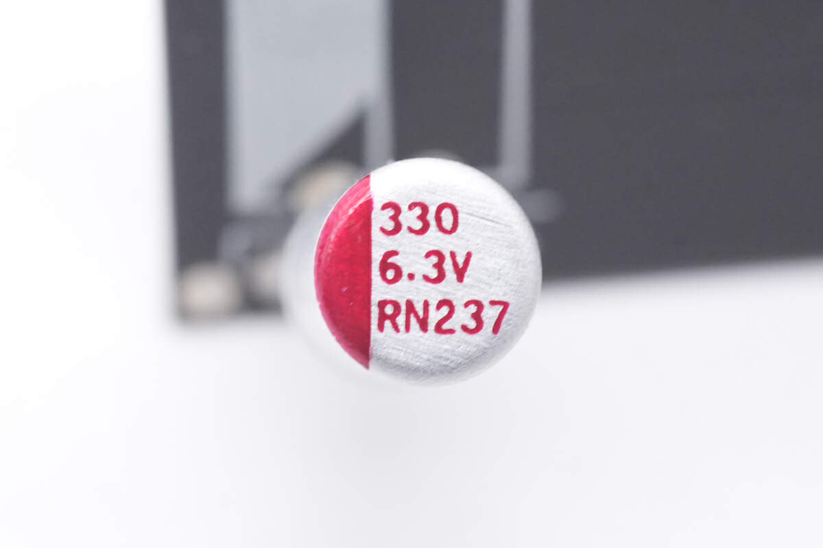
The solid capacitor is from PolyCap RN series. 330μF 6.3V.
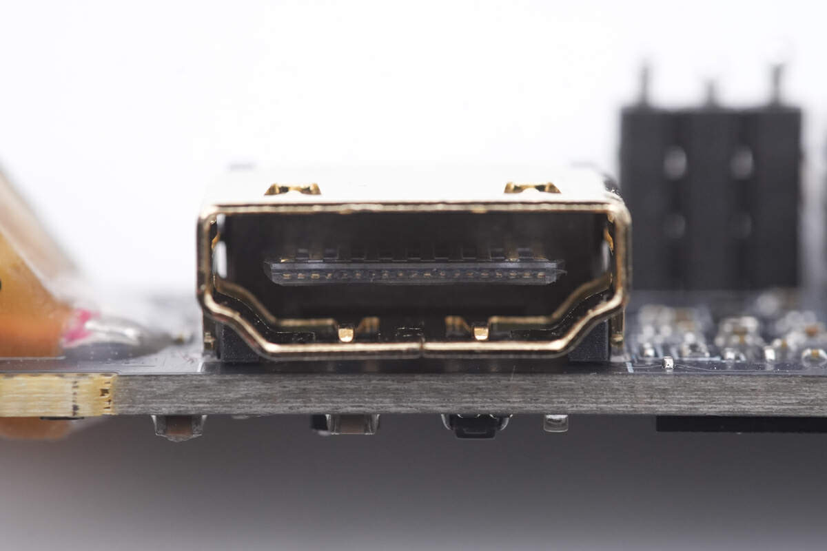
The HDMI socket is soldered on the PCBA.
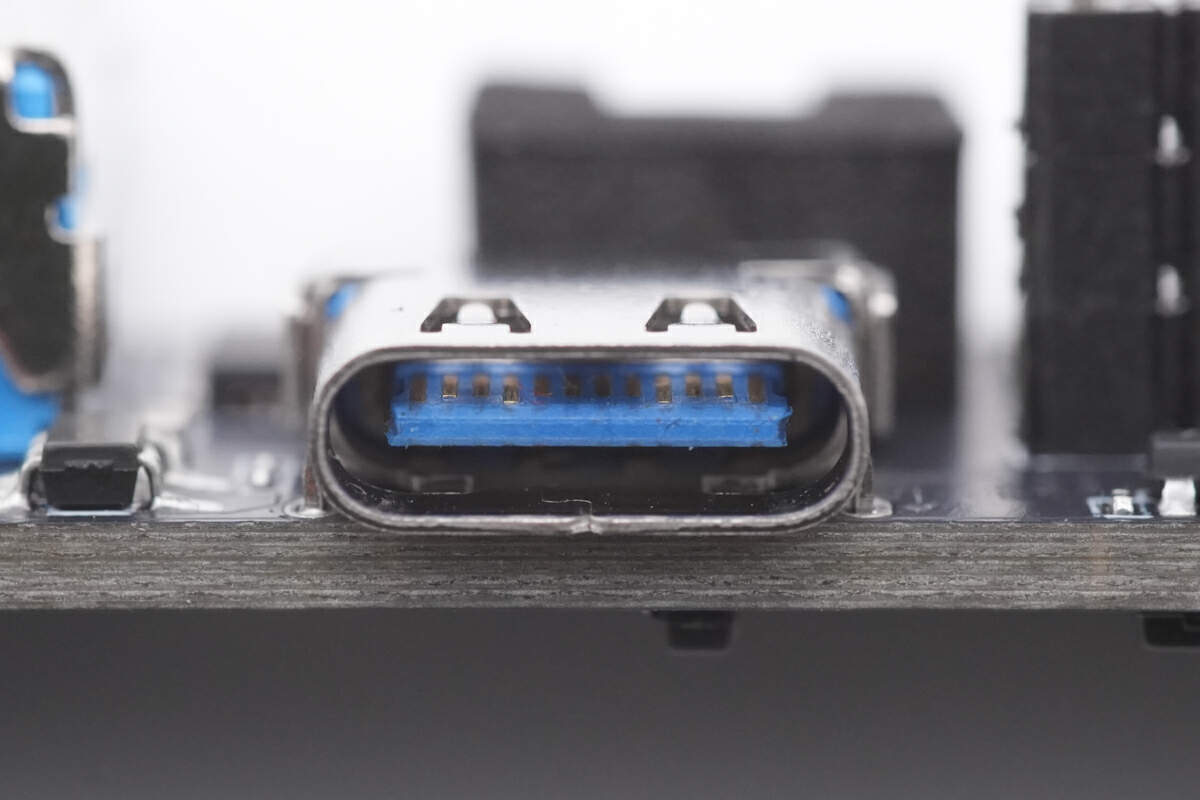
The plastic sheet of the USB-C socket is blue.
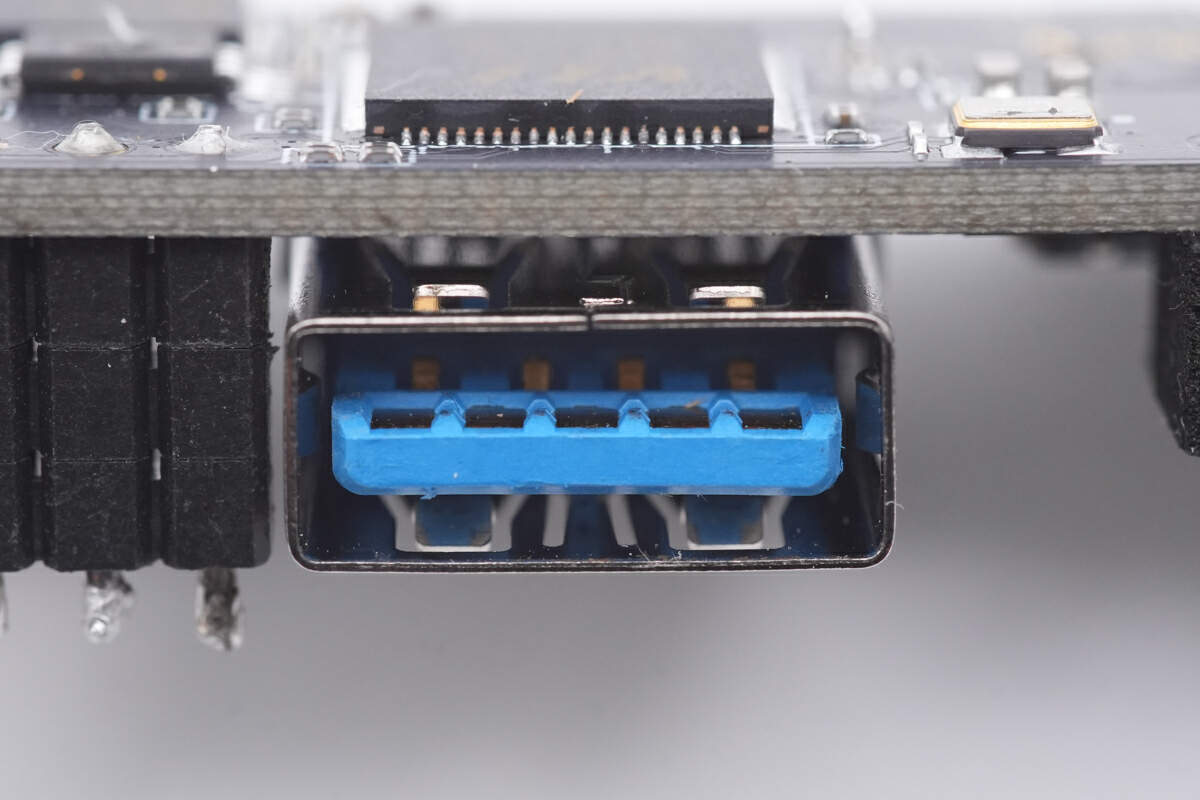
So is the USB 3.0.
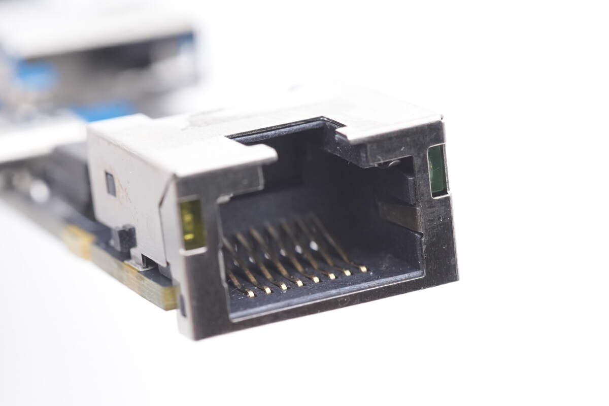
There are two indicator lights on both sides of the RJ45 port.
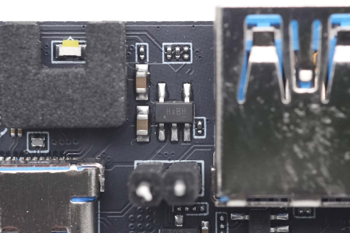
The overcurrent protection chip for the USB-A port is from ETA. Model is ETA6280. 6.1V 2A.
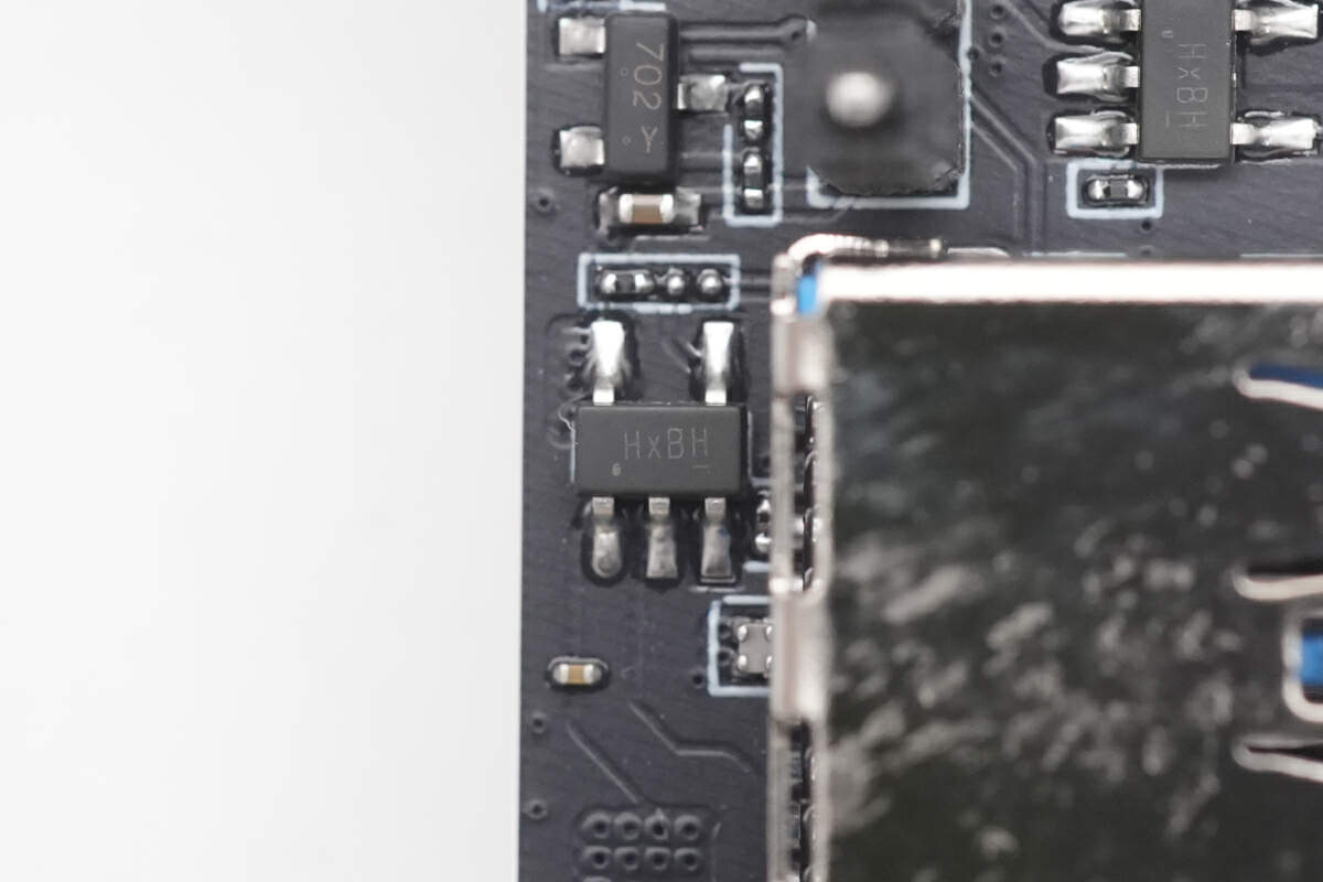
The other overcurrent protection chip for the other USB-A port has the same model.
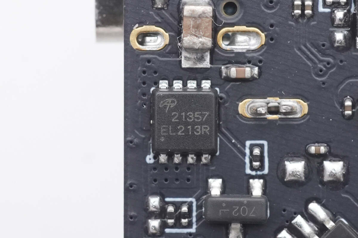
The MOSFET from AOS is used for power supply control and adopts DFN3 x 3 package. Model is AONR21357. 30V 6.3mΩ.
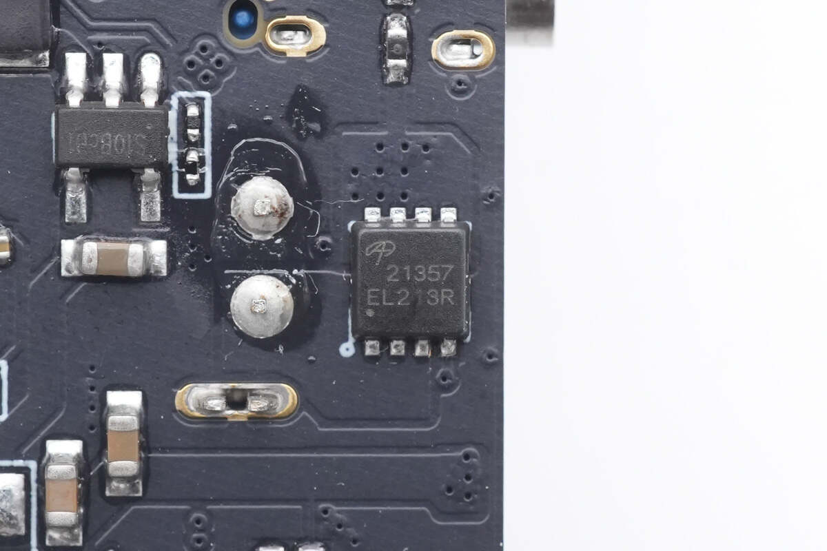
The other MOS has the same model.

Well, that's all components of the Anker 6-in-1 USB-C hub.
Summary of ChargerLAB
The hub has two USB-A ports, one USB-C port for power supply, one USB-C port for data transfer, one HDMI port, and a RJ45 port. The built-in cable can also charge the connected devices while using.
It adopts an aluminum case and three chips for port control and other functions. It also has an HDMI converter and Ethernet controller.
The multiple ports it has can meet regular usage needs.
Related Articles:
1. Transformers Inside | Anker Launched 65W GaNPrime 733 Power Bank
2. Phone Stand Included | Anker Unveils 335 Power Bank
3. Teardown of Anker 140W PD3.1 Power Bank (737 Power Bank)

