Introduction
Hey everyone, I hope you're all as excited as I am for today's teardown! It's been a little while since we last explored the inner workings of a device. So today, we gonna take apart a 150W GaN charger from the Anker GaNPrime series.
What sets this charger apart is its impressive capability with not just one or two, but three USB-C ports, alongside a USB-A port. With this configuration, you can simultaneously fast charge up to four devices. We can also call it "747 Charger".
Product Appearance
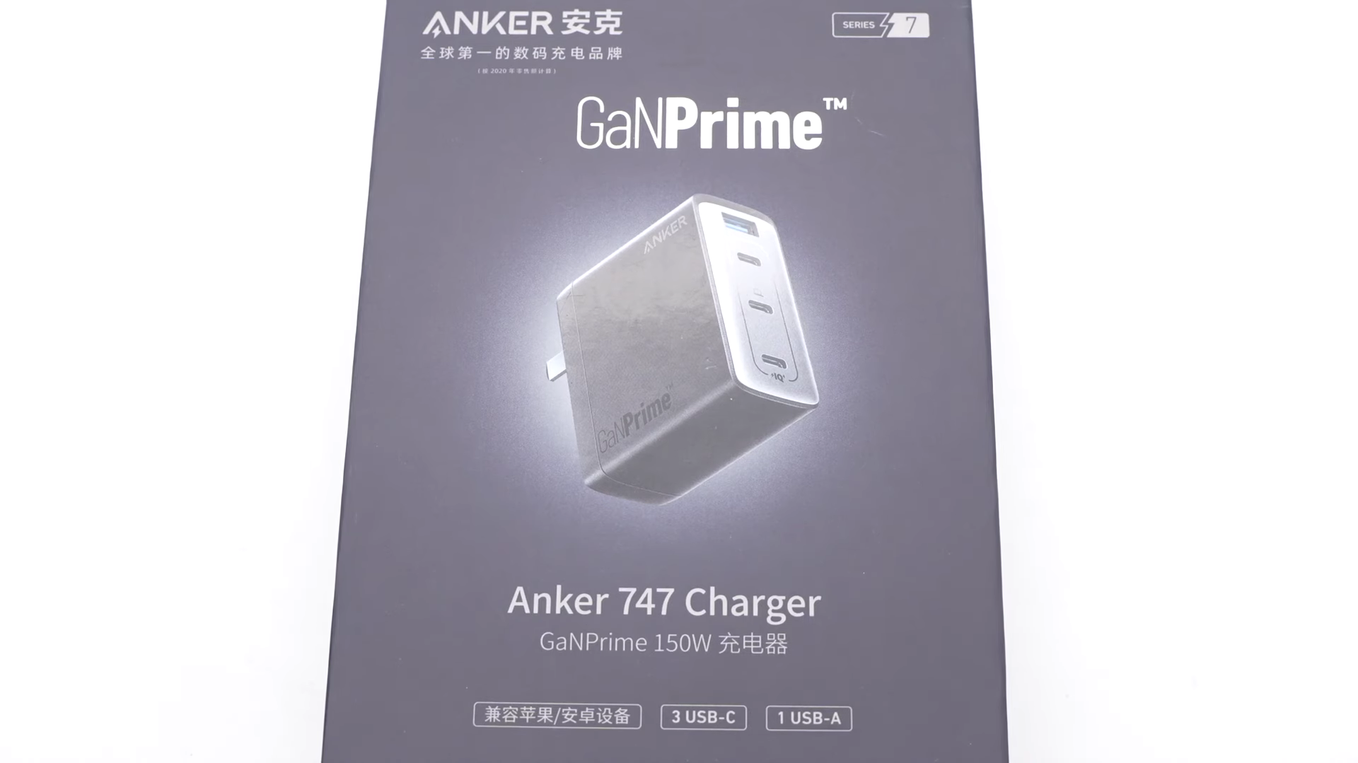
The packaging box continues the GaNPrime series' design style, featuring an all-black background with the product's appearance showcased in the center.

The back of the box highlights the main selling points of the product.
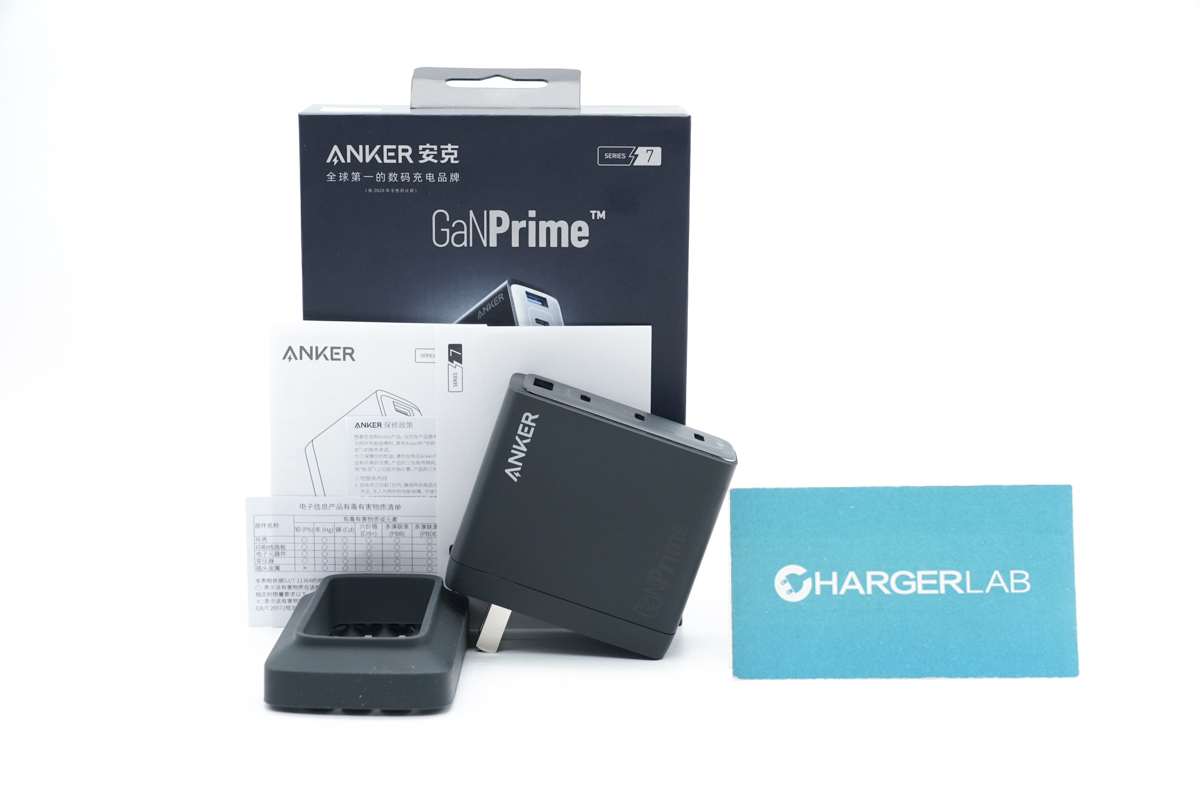
Inside, you will find the charger, a silicone stabilizer, and some documents.
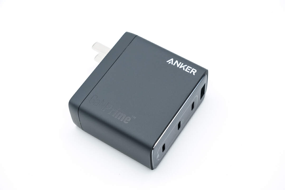
Then, let's introduce this charger. The black outer case feels smooth.
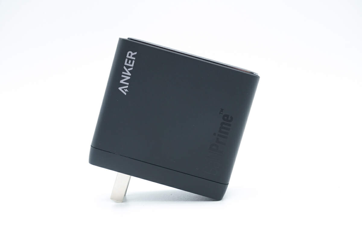
ANKER and GaNPrime are printed on the upper right and lower left, respectively.
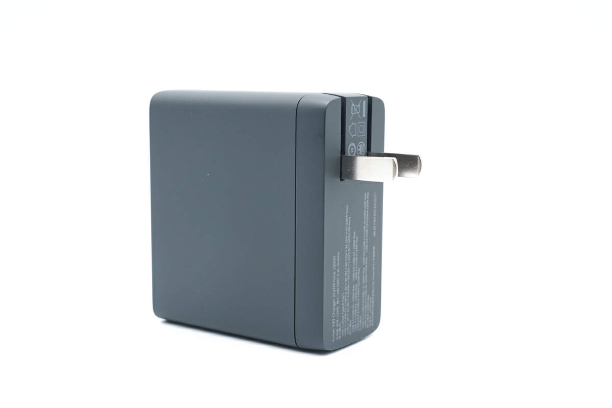
The input prongs can be folded for better portability.
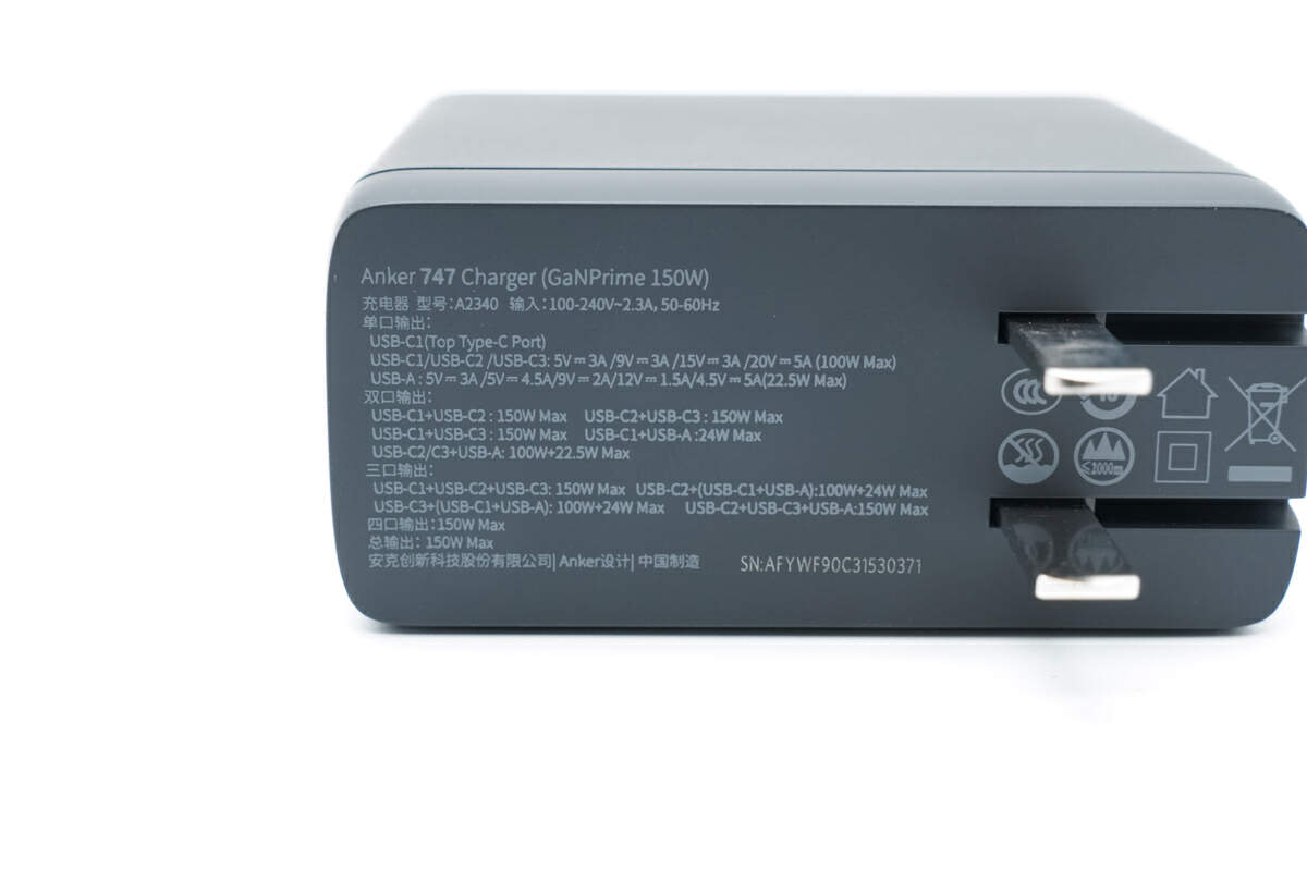
All specs info are printed at the bottom. Model is A2340. It supports input of 100-240V~50/60Hz 2.3A.
For single-port charging, all three USB-C ports support up to 100W, and the USB-A only supports 22.5W. Things get more complicated when charging two devices. It can provide up to 150W for two USB-C devices, and do not charge with USB-C1 and USB-A at the same time, cause the power drops to 24W. As for three-port charging, the output power will be divided into 150W or 124W. Even if we charge four devices at the same time, the power will not exceed 150W.
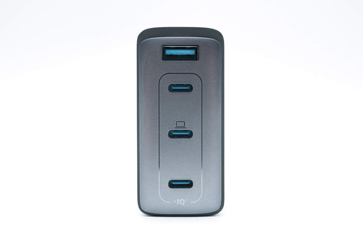
The silver output panel continues Anker's design, with the iQ4 logo at the bottom.

The silicone stabilizer has numerous suction cups at the bottom, designed for secure fixation.
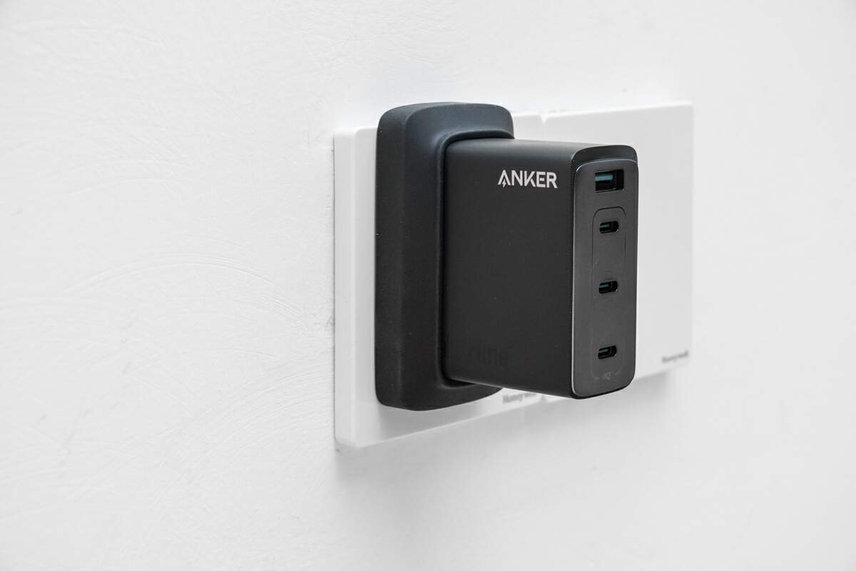
Once combine with the charger, it can firmly adhere to the wall outlet panel.
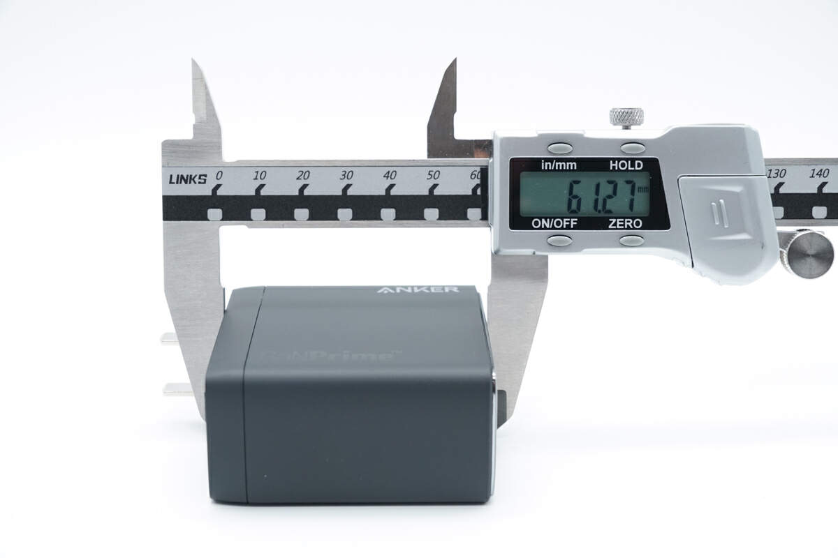
The length of this charger is about 61mm (2.4 inches).
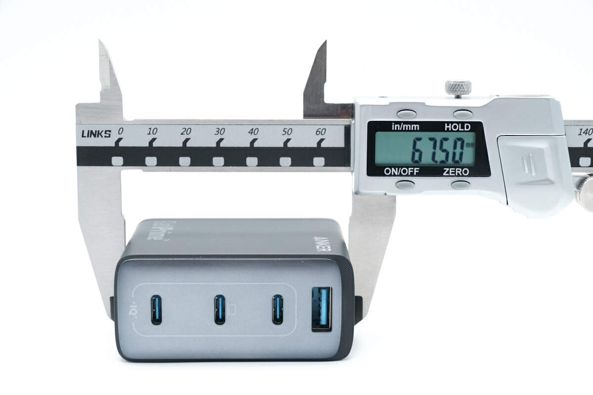
The width is 67.5mm (2.66 inches).
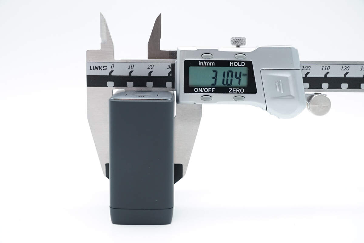
And the height is 31mm (1.22 inches).
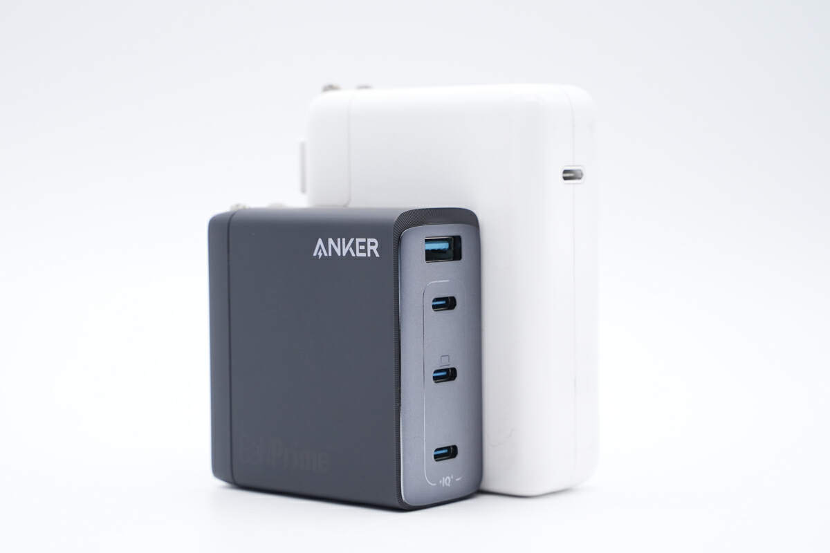
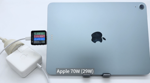
Compared with Apple 140W charger, it's smaller but a little bit thicker.
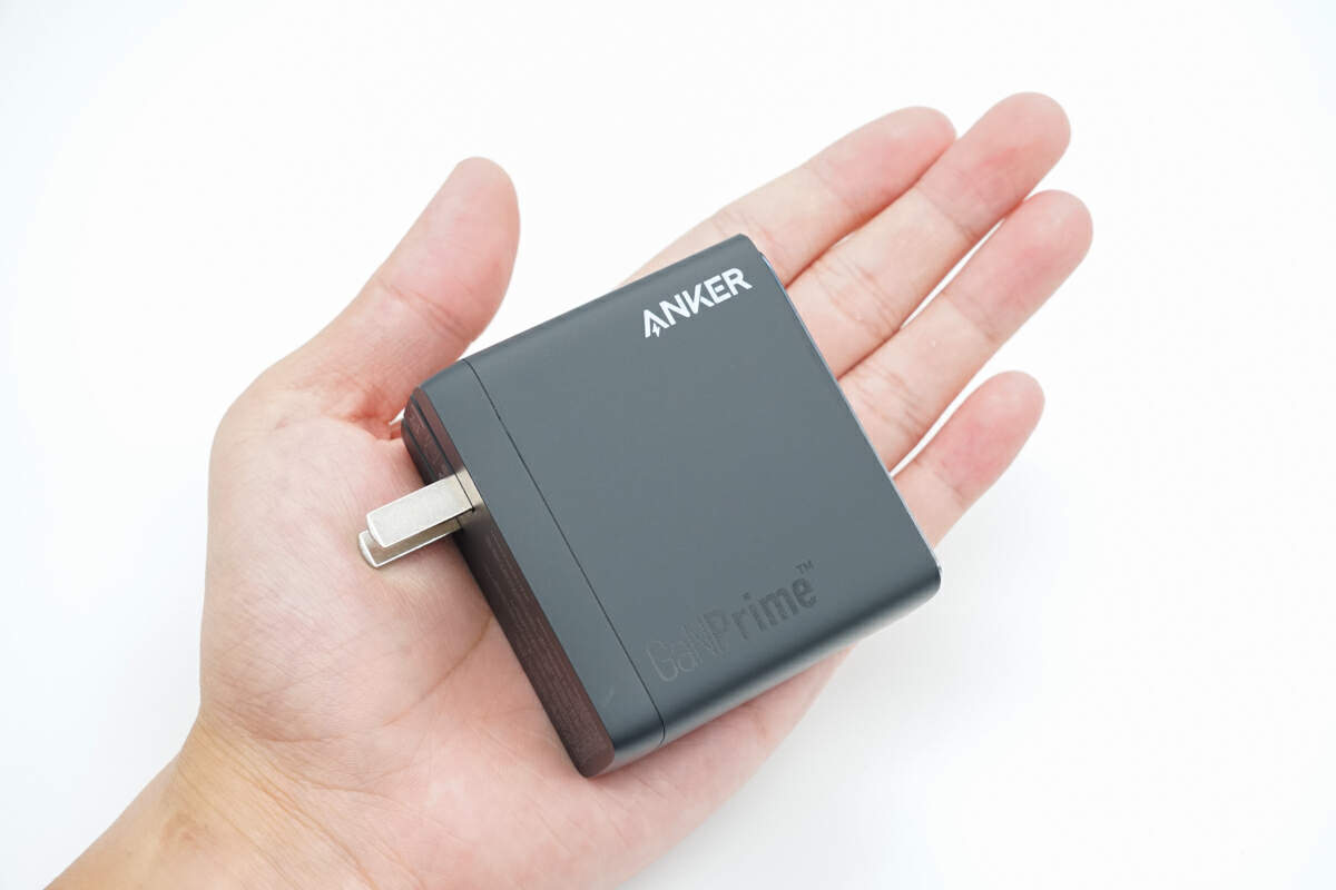
This is how it looks like on my hand.
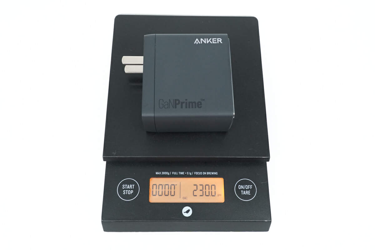
And the weight is about 230g (8.11 oz).
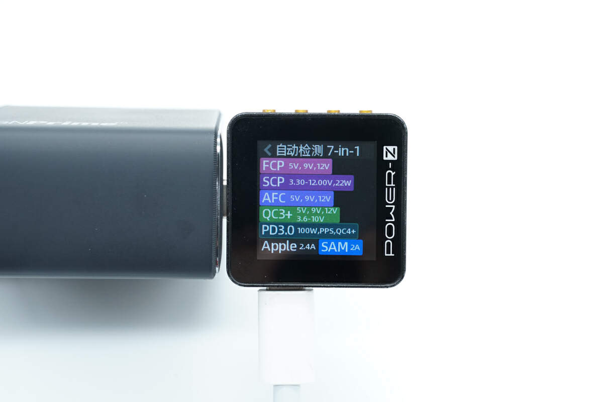
The ChargerLAB POWER-Z KM003C shows the USB-C1 supports FCP, SCP, AFC, QC3+/4+, PD3.0, PPS protocols.
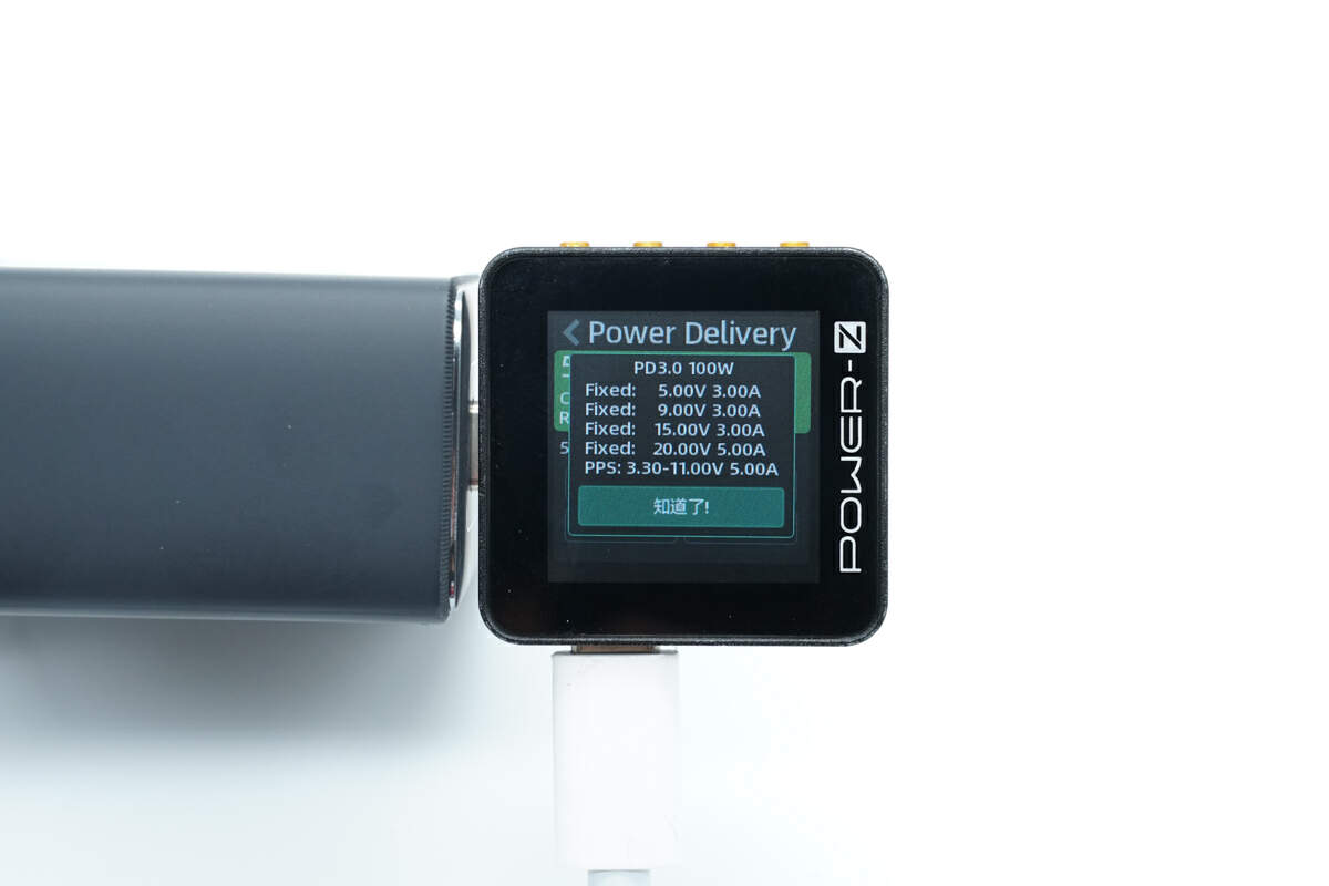
And it also supports four fixed PDOs of 5V/9V/15V 3A, 20V 5A, and a set of PPS.
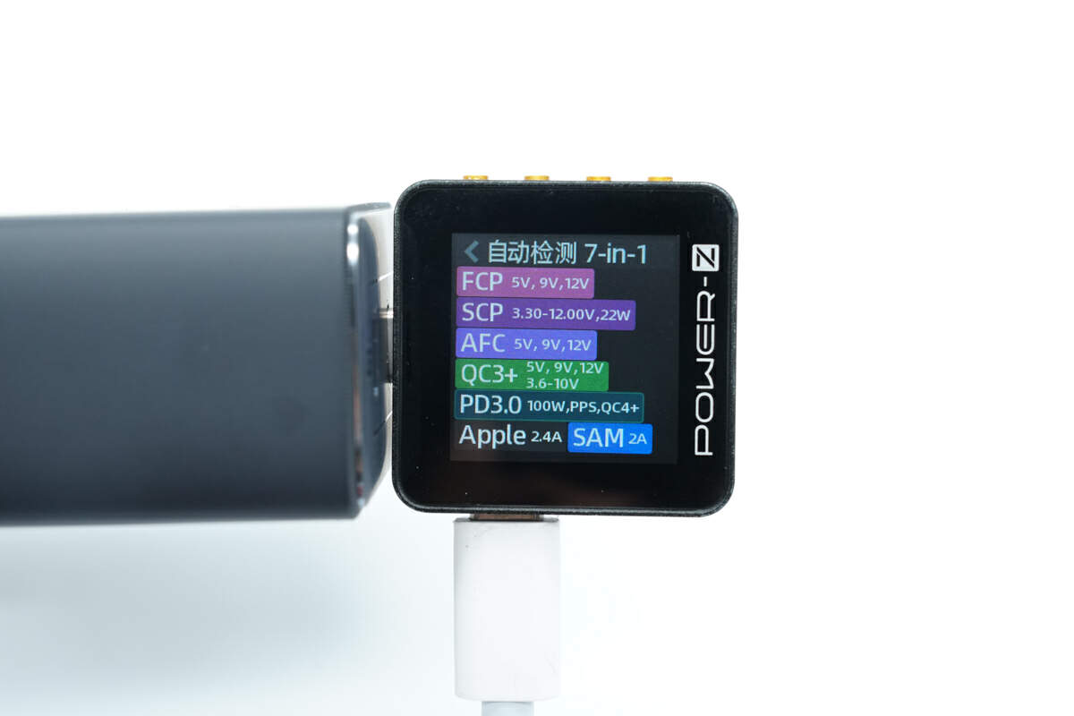
The supported protocols of the other two USB ports are the same as the USB-C1.
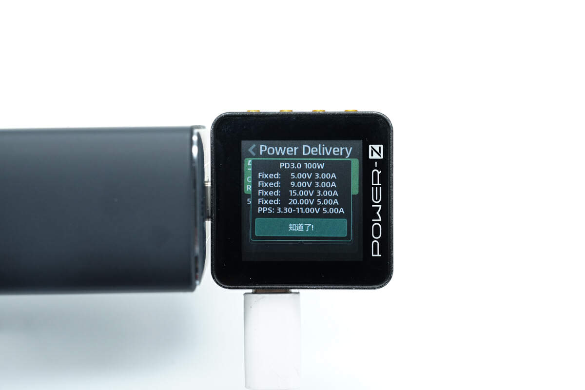
So is the PDO info, which means you can choose any USB-C port to get the 100W.
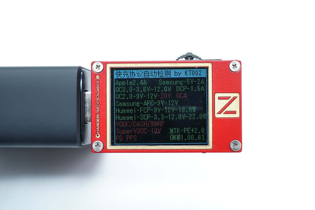
As for the USB-A, it supports FCP, SCP, AFC, QC3+, DCP protocols.
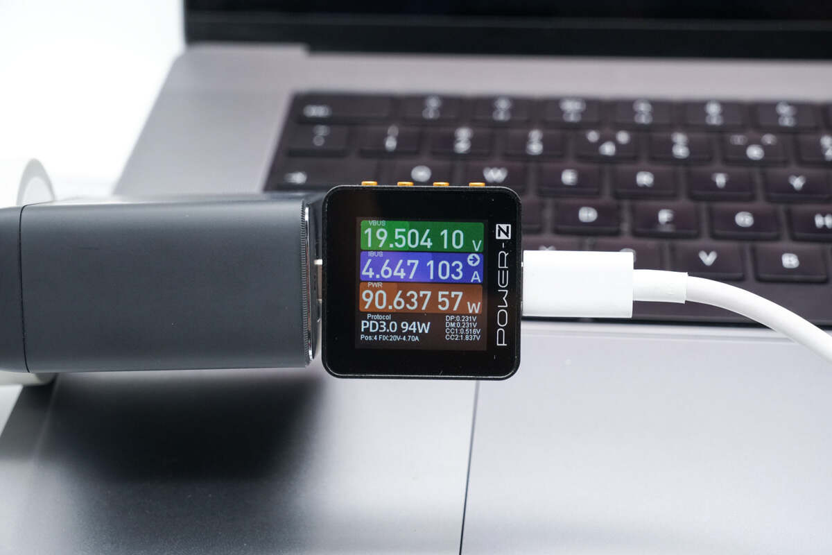
For example, the USB-C1 can provide 90W to the MacBook easily.
Teardown

Next, let's use the cutting machine to remove the outer shell.

The thermistor is attached to the plastic case.
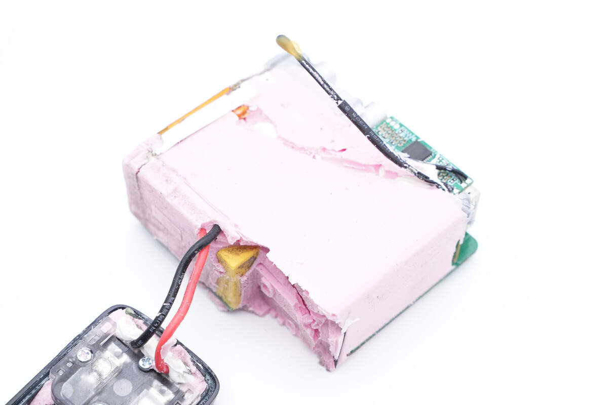
The entire module is covered with pink potting compound for better heat dissipation and mechanical strength.

And disconnect two input wires.
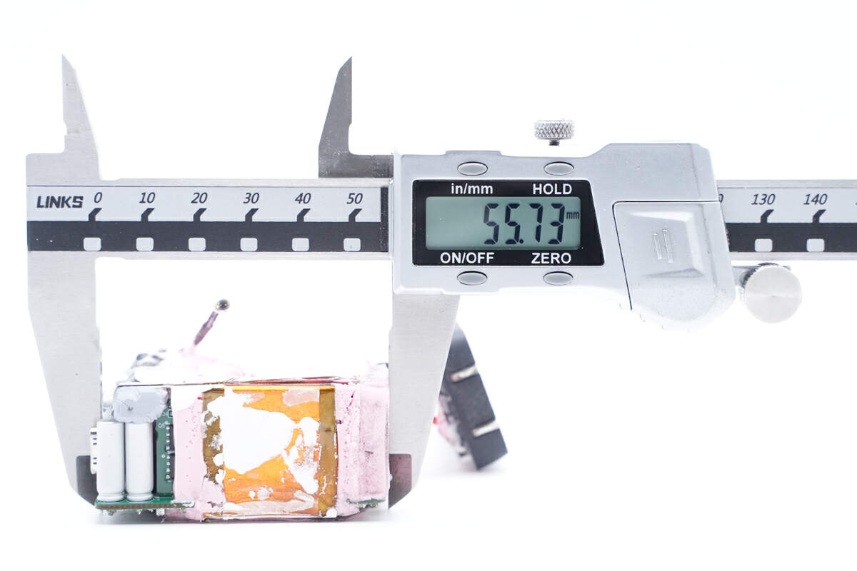
The length of the PCBA is about 55.7mm (2.19 inches).
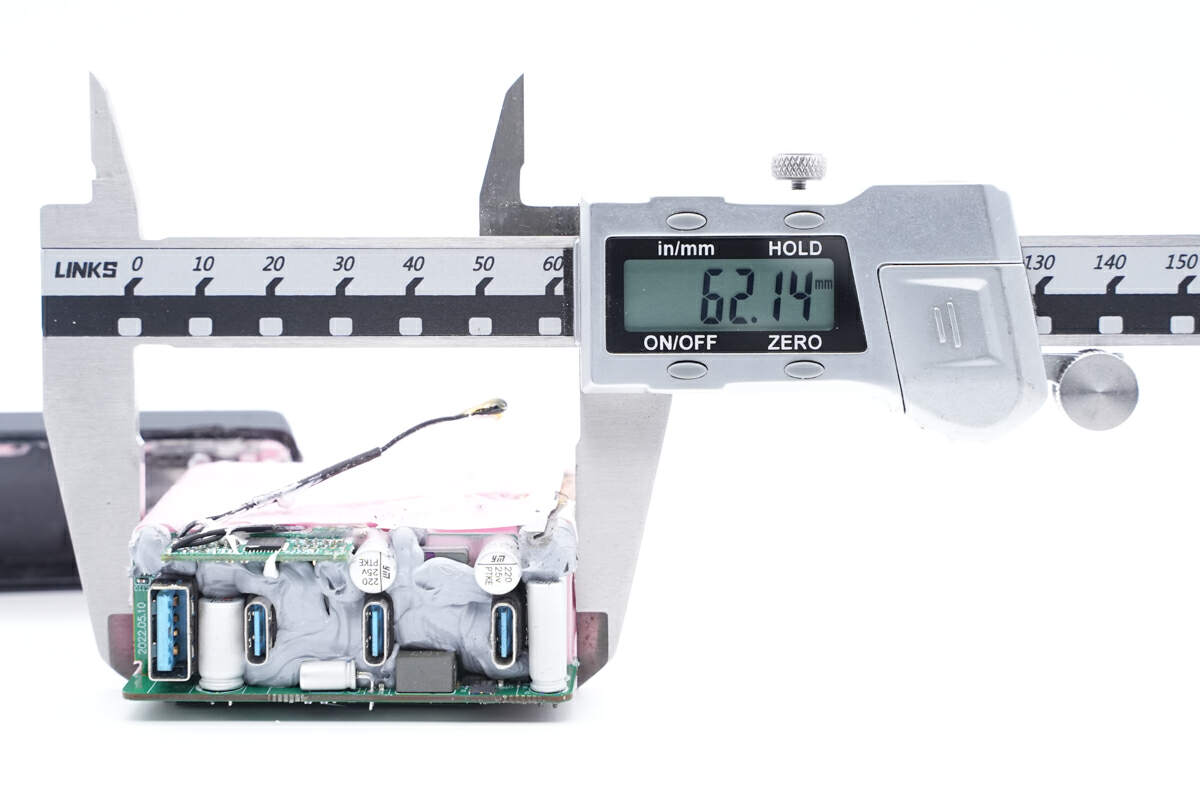
The width is about 62mm (2.44 inches).
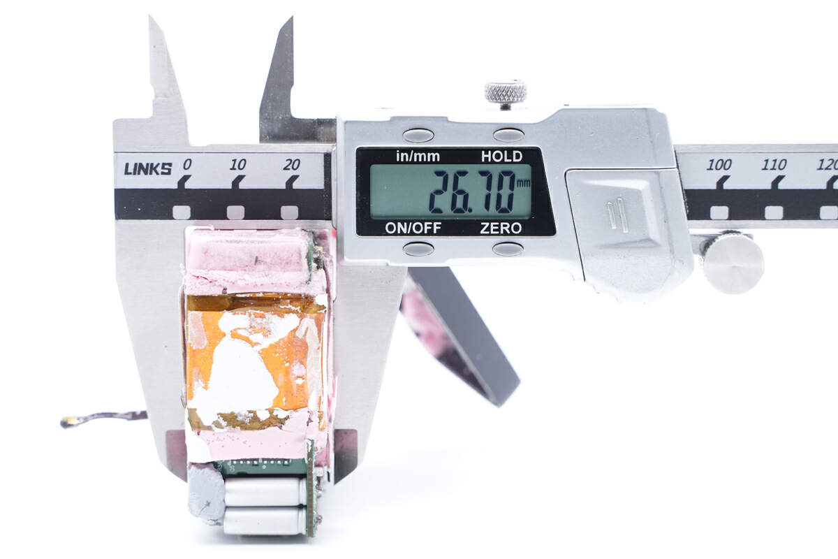
And the height is about 26.7mm (1.05 inches).
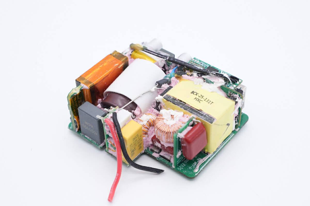
Let's clean up the module first. Its interior has been upgraded from the traditional flat layout to a three-dimensional layout, allowing for optimal space utilization and reducing its overall size.
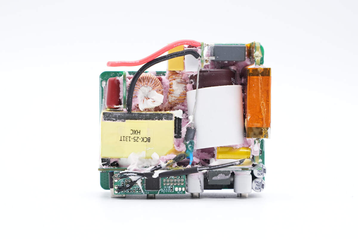
Then, let's introduce this PCBA module and all components to you. The fuse, EMI filter circuit, PFC boost inductor, and a flat transformer are located on the front side of the PCBA module.
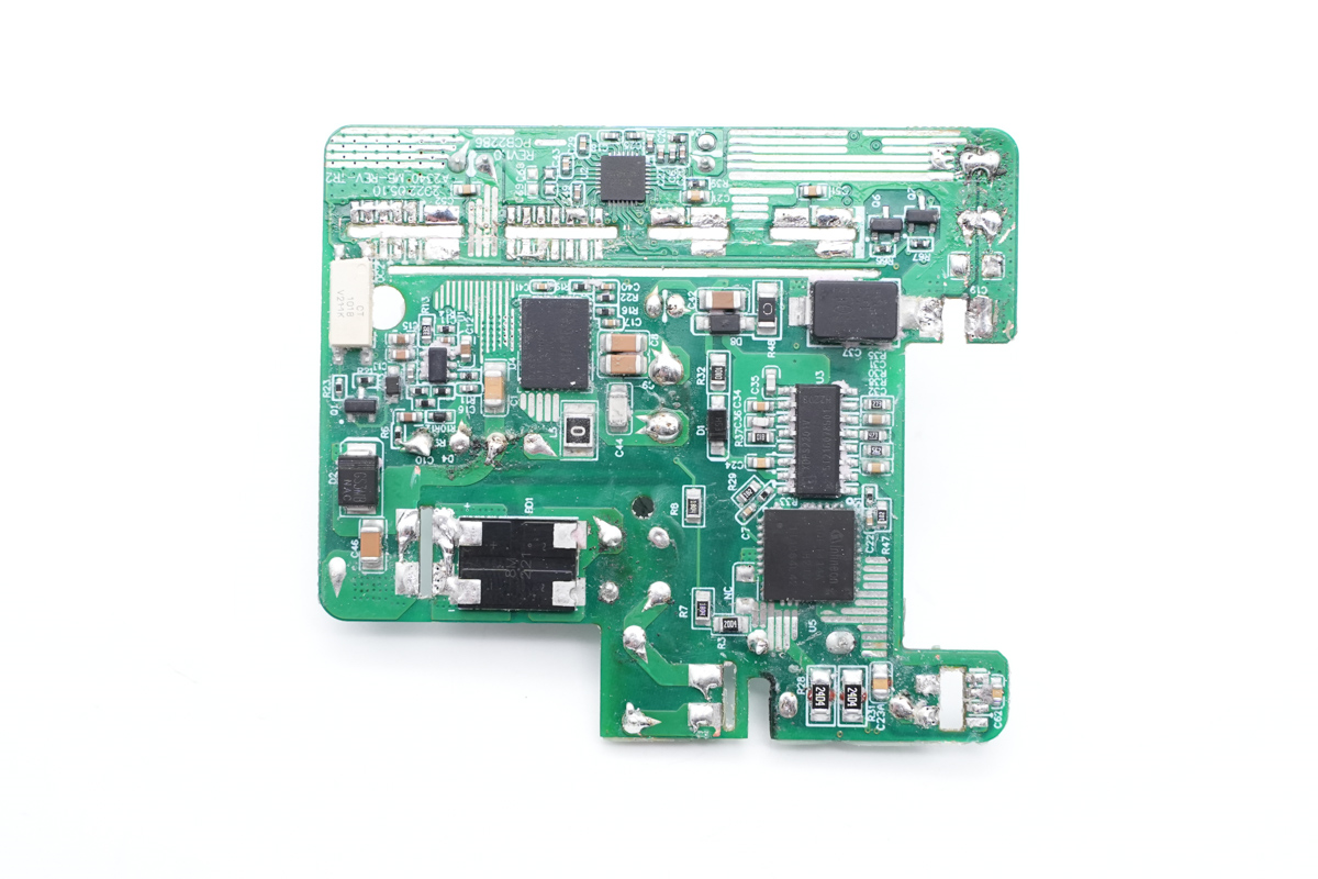
There's a groove between the primary and secondary circuits. And the Bridge rectifier, PFC boost controller, Navitas GaN IC, SMD Y capacitor, and buck chip are situated on the backside.
ChargerLAB found it adopts Hybrid-flyback topology and has a PFC circuit, and the output utilizes three synchronous buck circuits, enabling fast charging output for four ports.
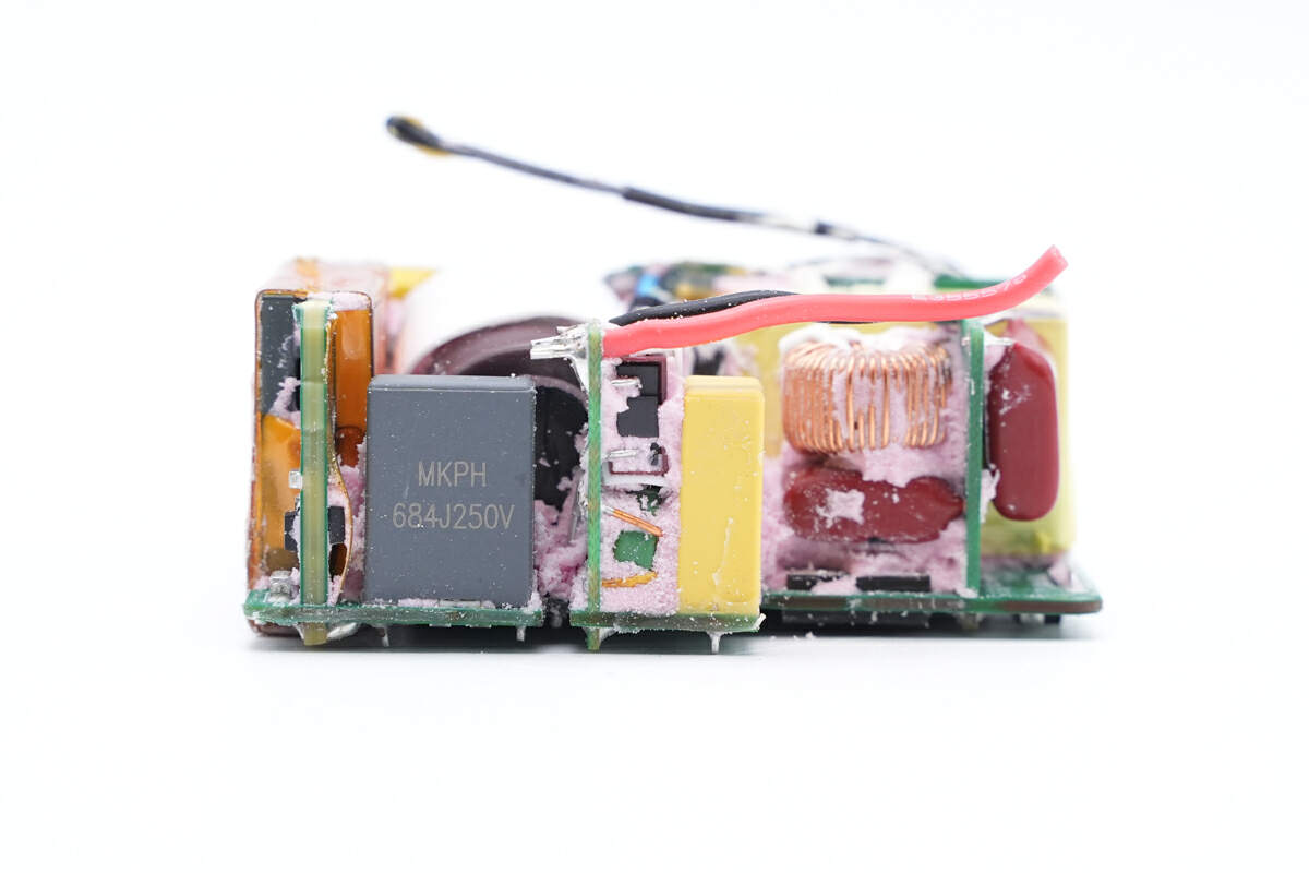
Next, we will begin to learn the design and materials used in the entire charger, starting from the input end.
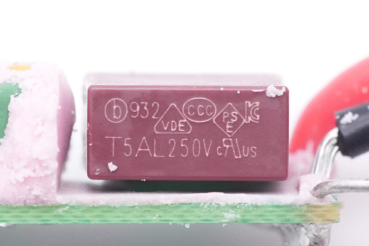
The 932 time-delay fuse is from BetterFuse. 5A 250V.
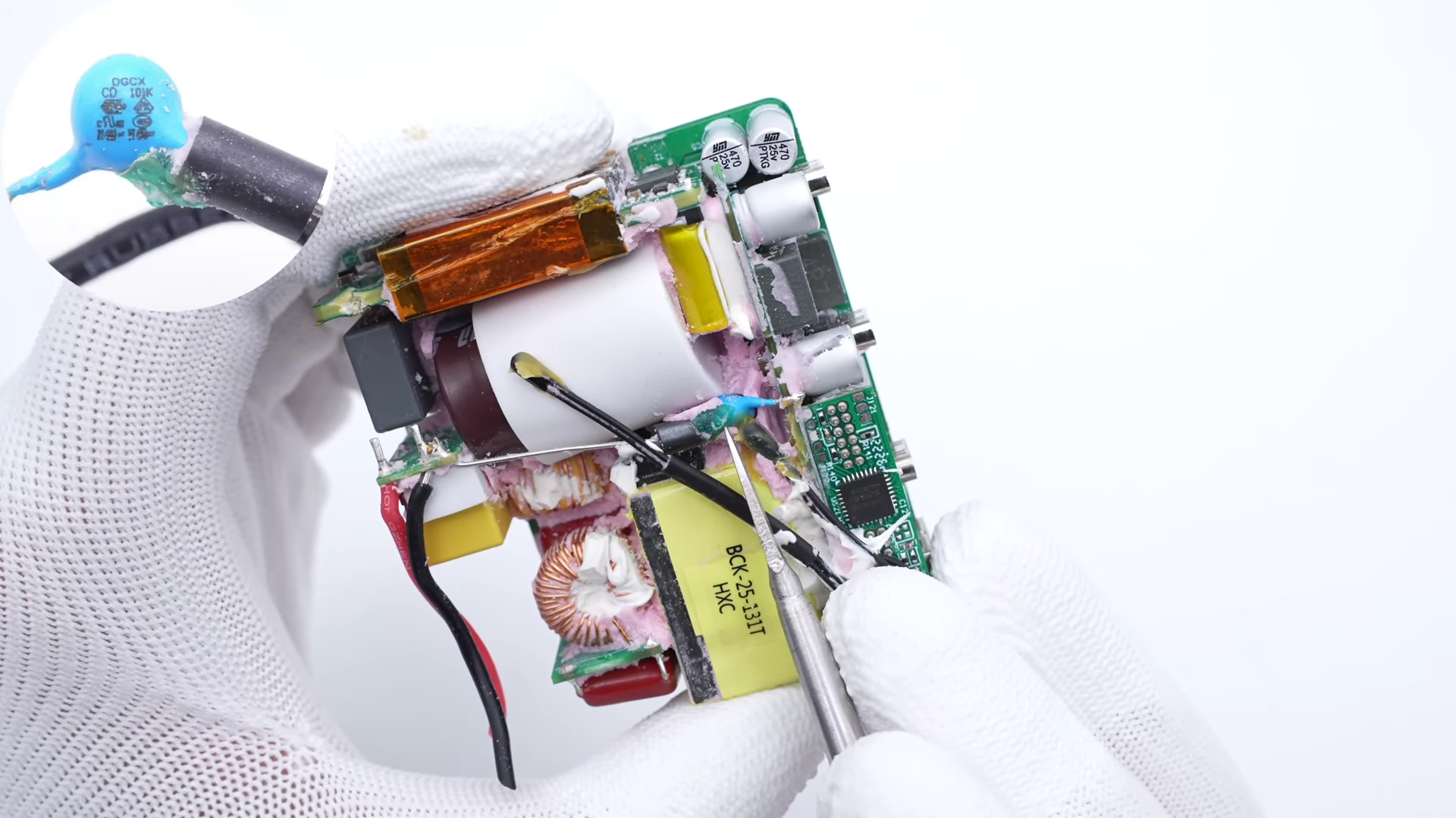
The blue Y capacitor from DGCX is located in the middle but is soldered to the input end.
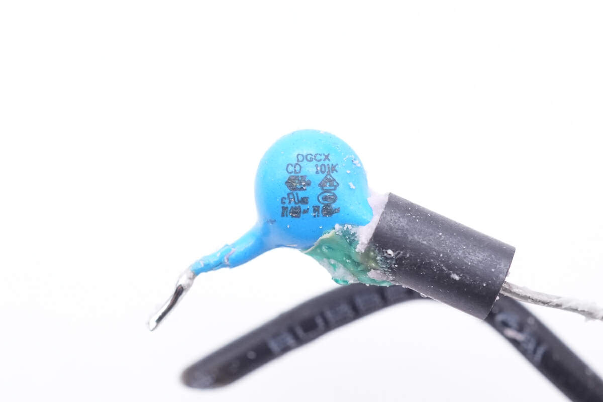
Take a closer look.
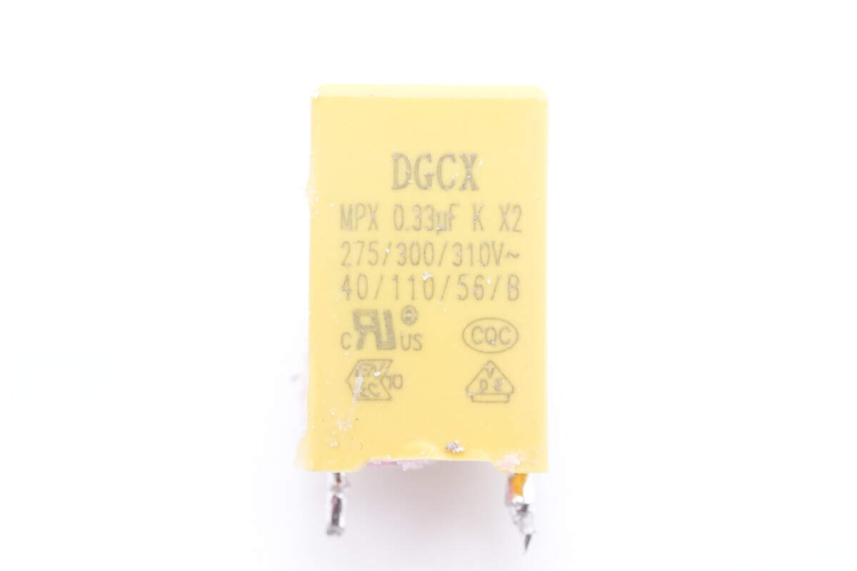
The safety X2 capacitor is also from DGCX. 0.33μF.
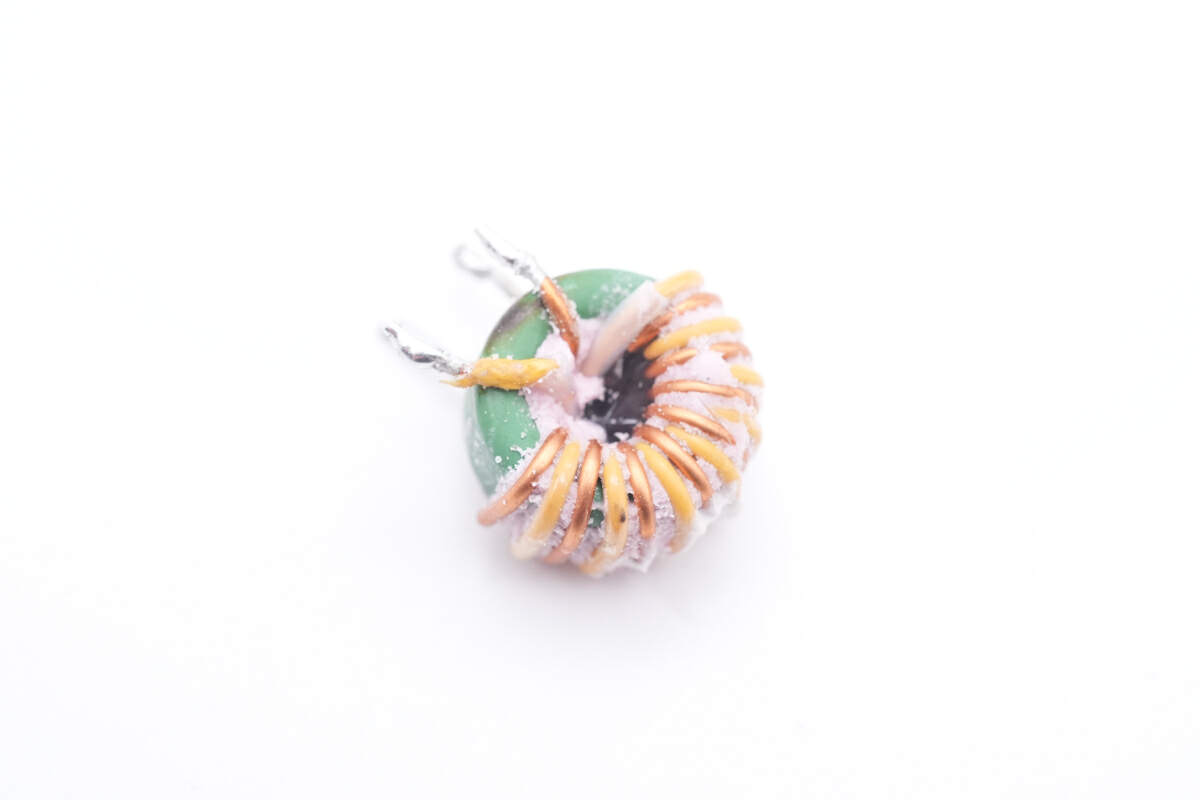
The first common mode choke is wound with magnet wires and insulated wires.
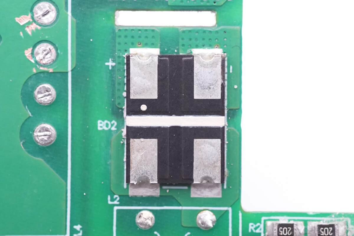
This is the diode on the front.
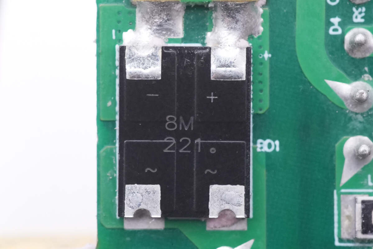
And another one on the back. They are connected in parallel to form a bridge rectifier and dissipate heat evenly.
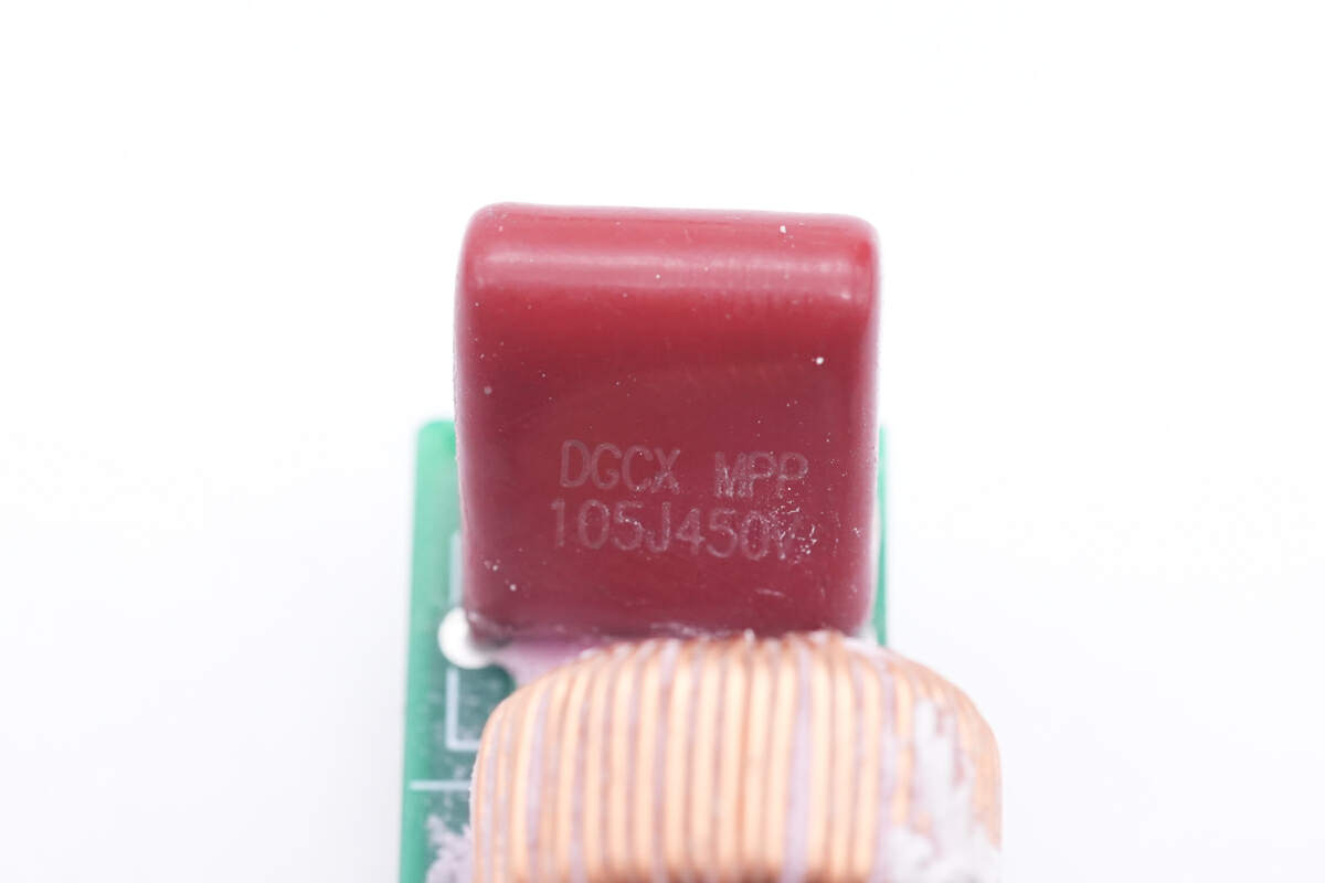
This film capacitor is from DGCX.
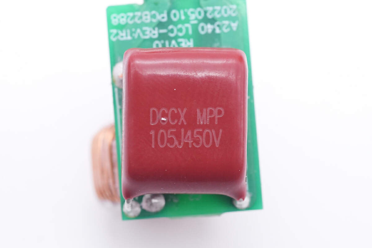
And another same film capacitor, 1μF 450V for each. The fluctuating DC will be filtered by them.
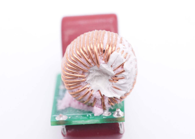
And here is the filter inductor.
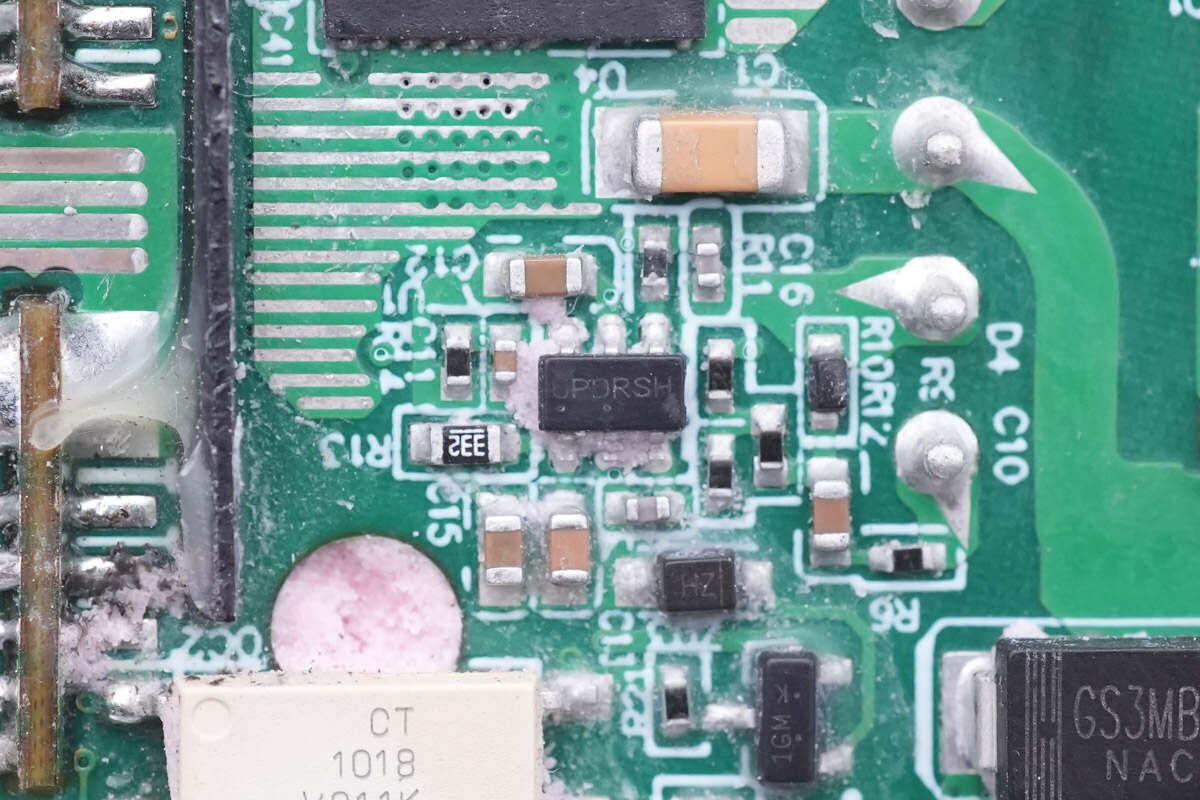
Then, let's see the PFC circuit. The PFC controller is from ON Semiconductor. The innovative VSFF (Valley Synchronous Frequency Foldback) maximizes efficiency at normal and light load. Model is NCP1623.
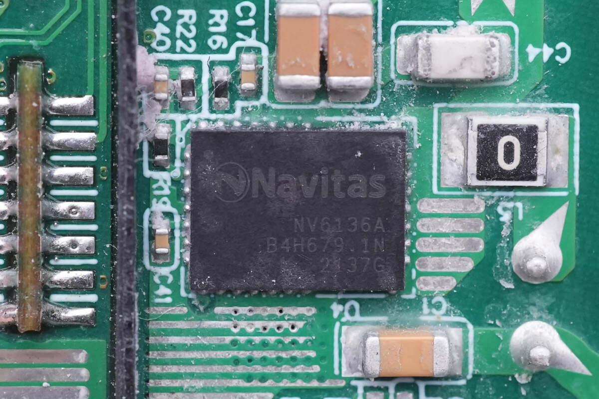
The GaN IC for PFC boost is from Navitas and adopts QFN 6 x 8 package. It is actually a new generation intelligent GaNFast IC that incorporates GaNSense technology. And it integrates the driver and current sampling circuit to reach high integration.
170mΩ, 700V. Model is NV6136A.
It supports a switching frequency of 2MHz and adopts a 6 x 8mm QFN package. 170mΩ 700V.
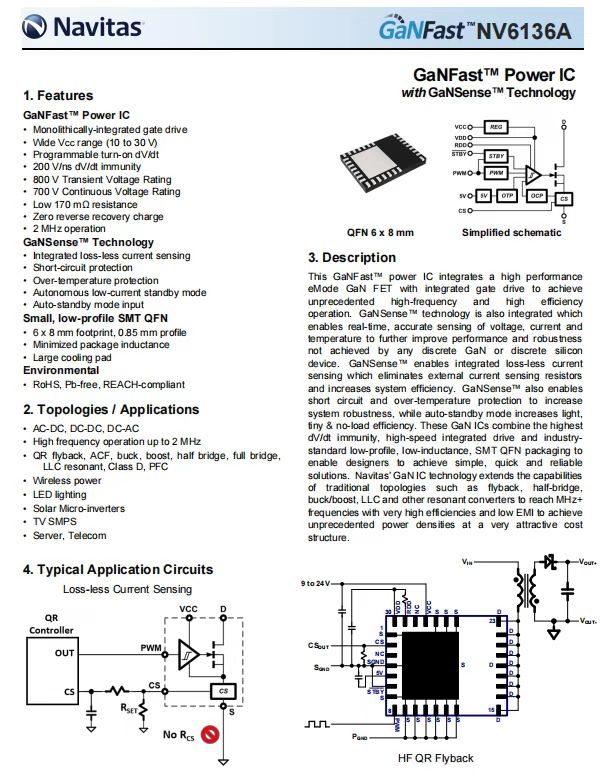
Here is all the information about NV6136A.
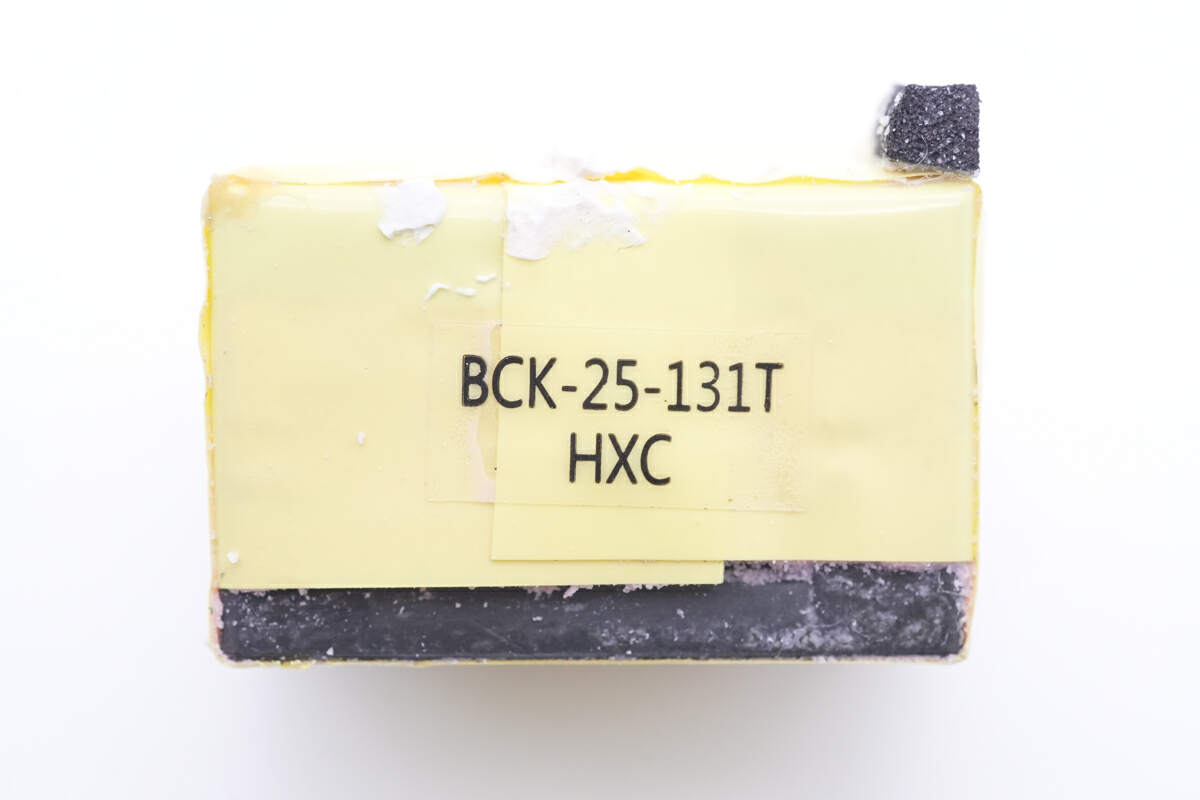
The PFC boost inductor is tightly wound and insulated with yellow tape.
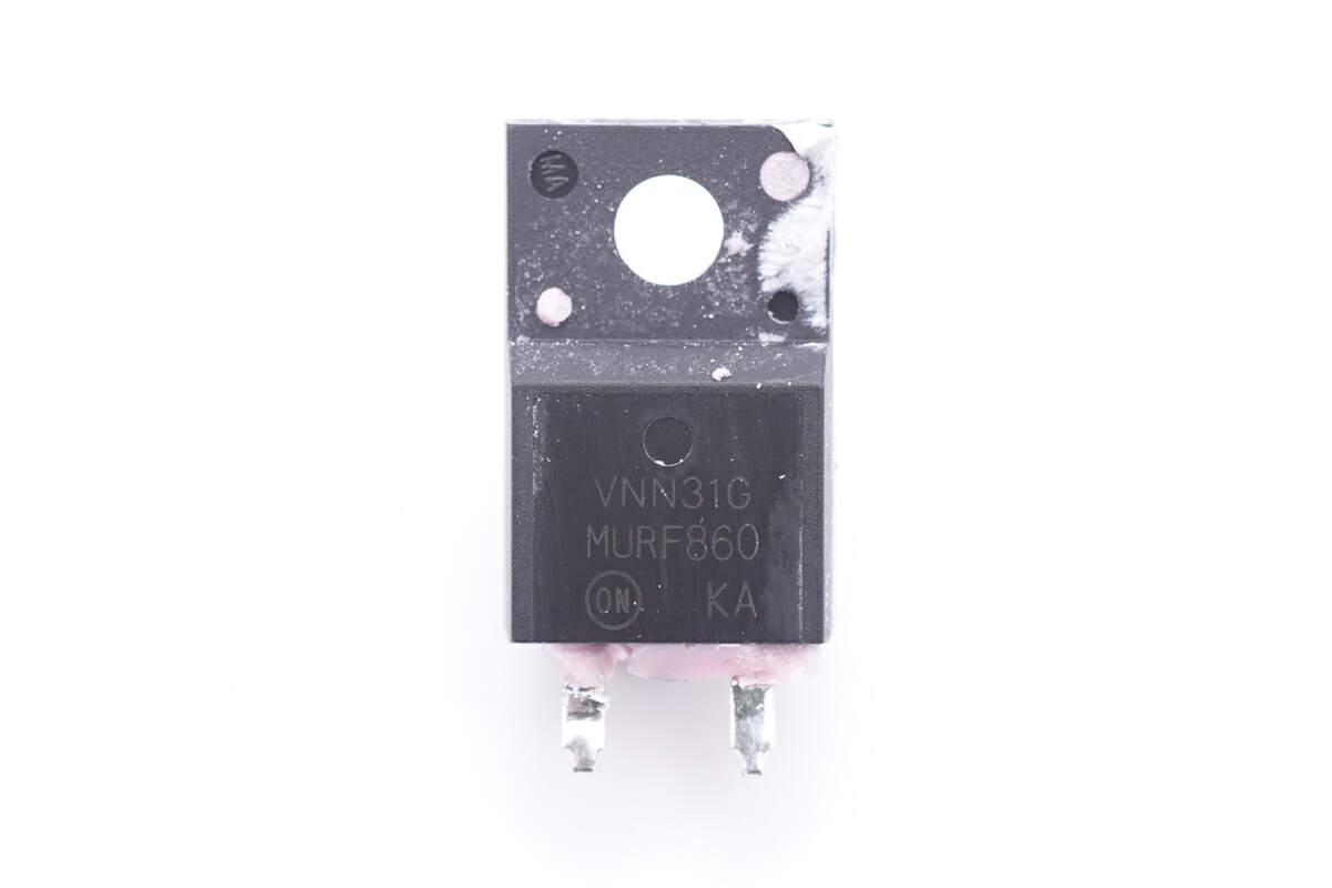
The PFC boost rectifier is from ON Semiconductor and adopts TO220FP package, model MURF860, it is actually an ultrafast recovery diode. 8A, 600V.
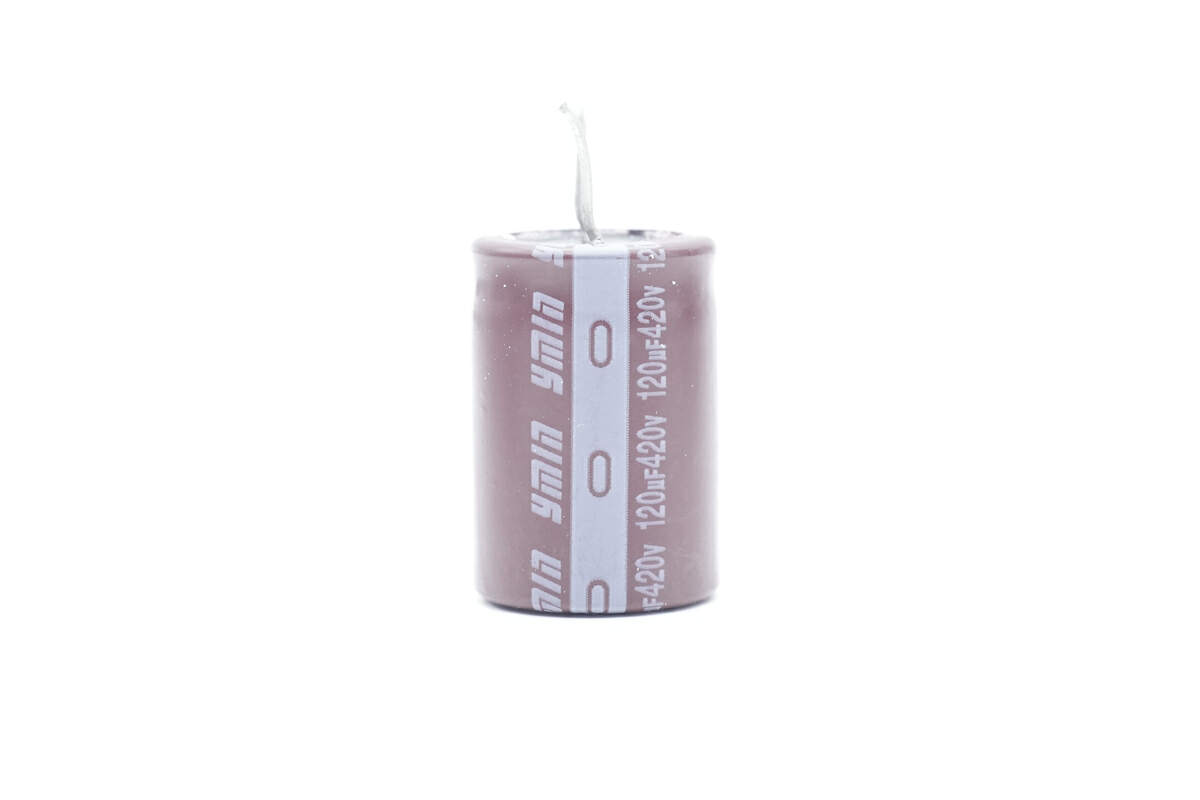
The largest electrolytic capacitor for input filtering is from Yongming. 120μF 420V.
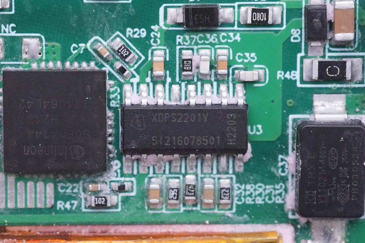
The primary controller for hybrid flyback topology is from Infineon and adopts PG-DSO-14 package. It integrates 600V high-voltage start-up and high-side & low-side MOSFET drivers. Model is XPDS2201.
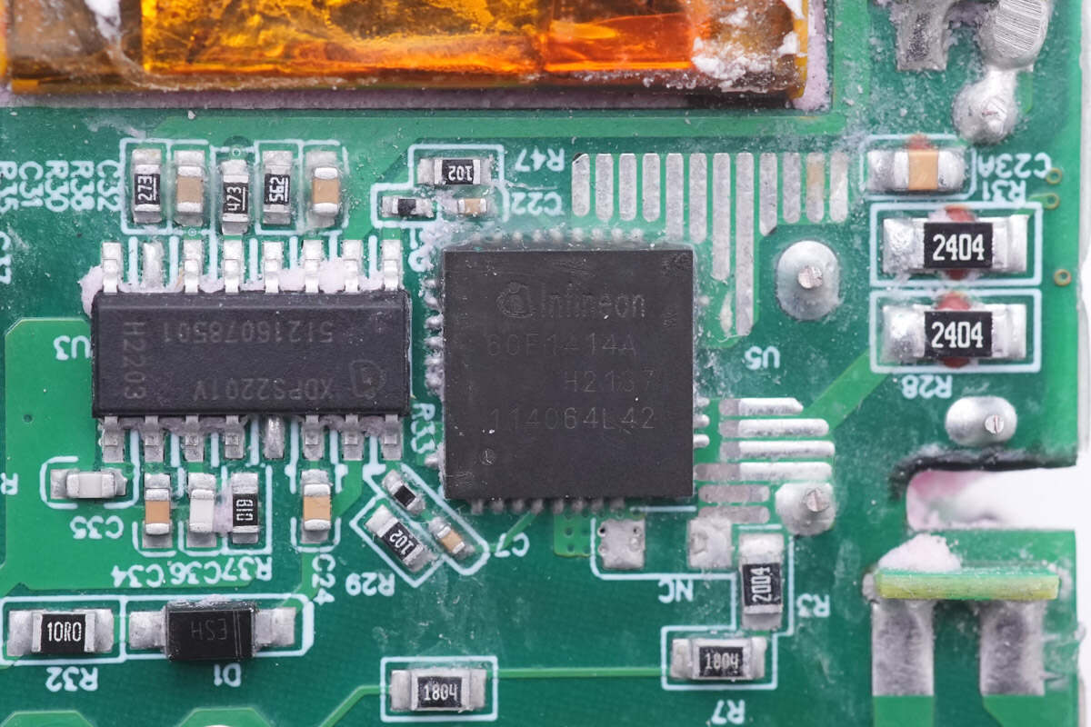
The primary GaN IC is also from Infineon. It integrates two GaN FETs and has an independent isolation driver, which greatly improves space utilization. 140mΩ, 600V for each. Model is IGI60F1414A1L.

The electrolytic capacitor that powers the primary controller is from Yongming. 47μF 35V.
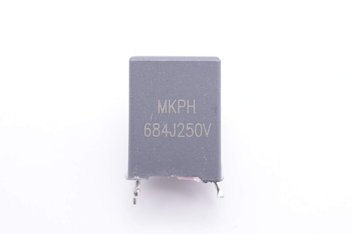
A resonant capacitor is connected in series with the primary side of the transformer. 0.68μF 250V.
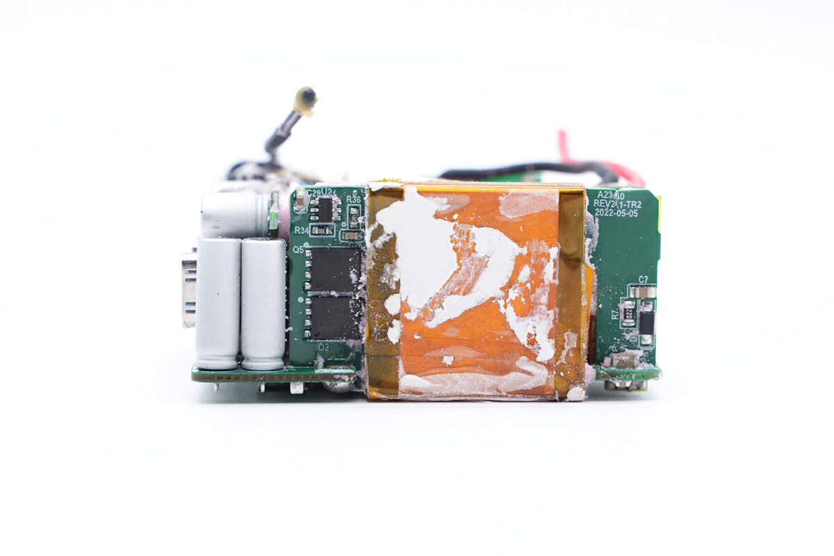
The flat transformer and output filtering capacitor are located on the side.
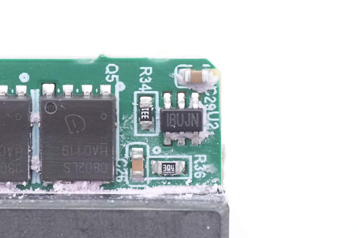
The synchronous rectification controller is from MPS and adopts TSOT23-6 package, model MP6951, it supports multiple working modes and topology, like active clamp flyback and hybrid flyback. The working frequency can be Up to 1MHz.
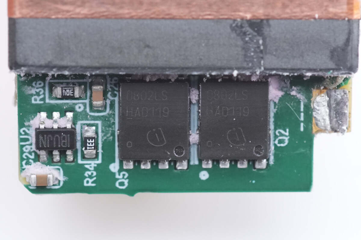
Those two synchronous rectifiers are connected in parallel, from Infineon. 100V, 3.4mΩ for each. Model is BSC0802LS.
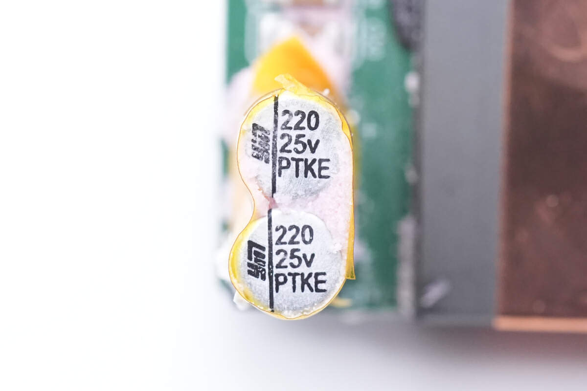
Two solid capacitors for output filtering are from Yongming VPT series. They're connected in parallel and are placed horizontally. 220μF 25V for each.
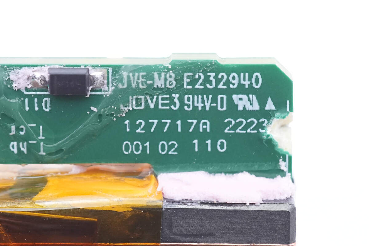
From the printed information, it can be seen that the flat transformer small board comes from JOVE.
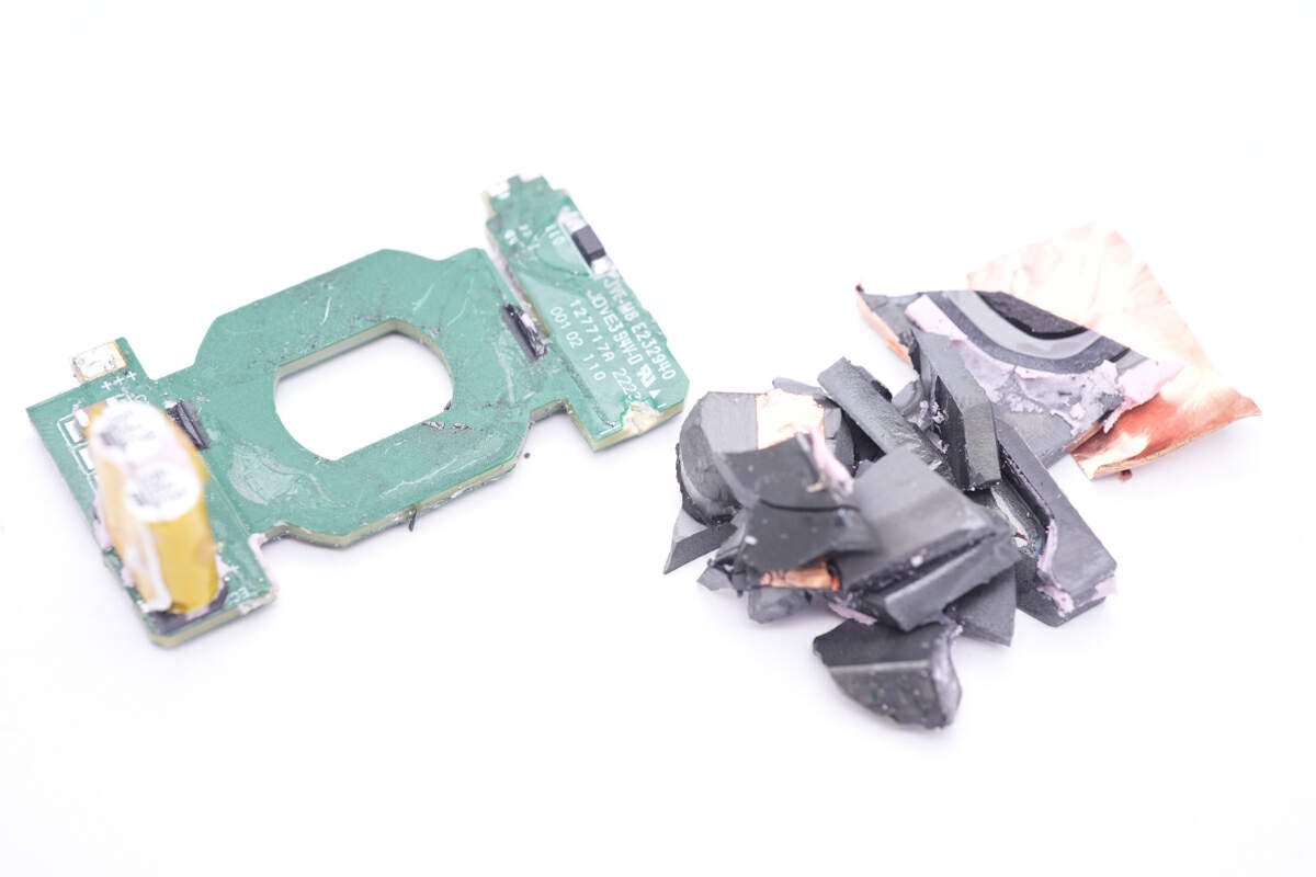
Next, smash the ferrite core of the flat transformer.
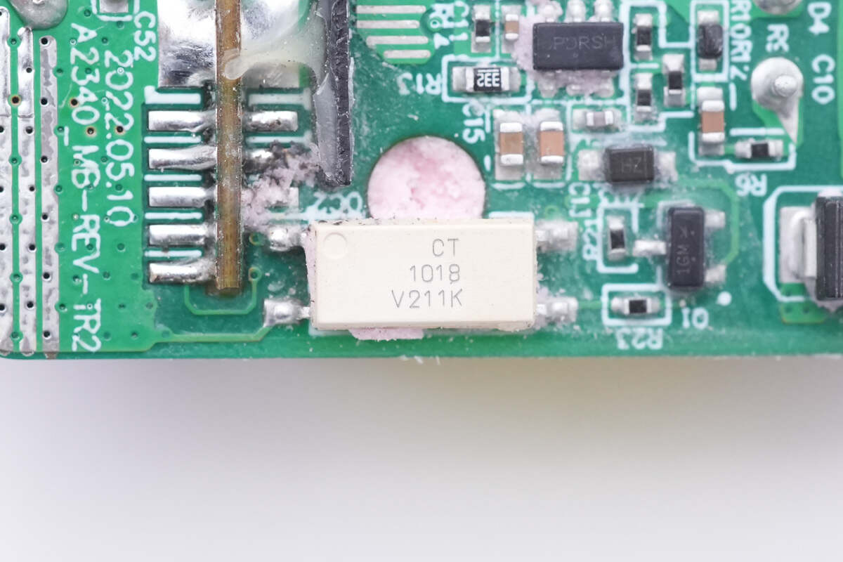
The CT1018 optocoupler is on the back of the PCB, used to regulate the output voltage.
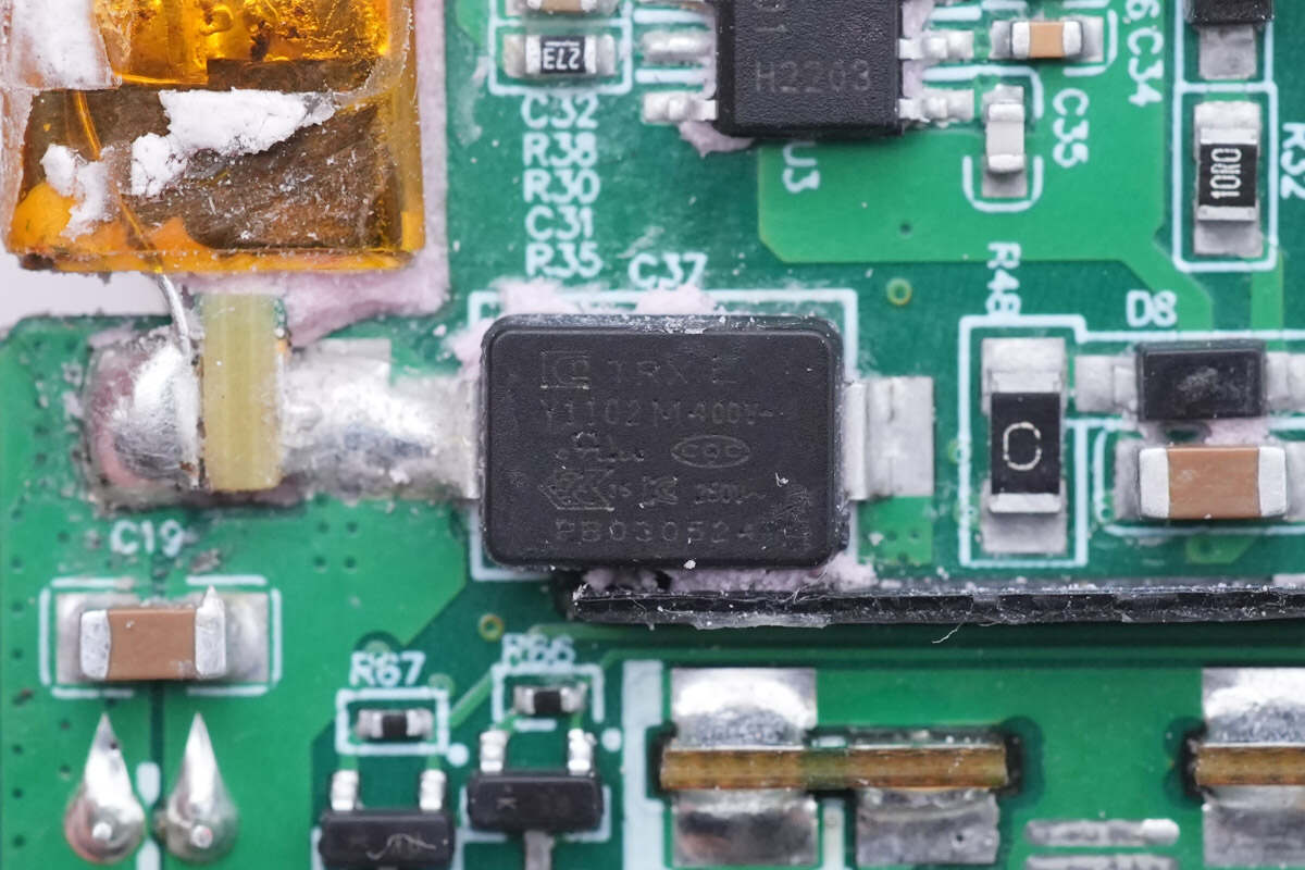
The SMD Y capacitor is from TRX, model TMY1102M, which features in small size and light weight, and are very suitable for high-density power supply products such as GaN charger.
TRX focuses on the R&D, production and sales of passive components, with a registered capital of 100 million yuan. It has two types of capacitor brands: SMD TRX and DIP TY capacitors. TRX will devote itself to the research of ceramic materials in order to provide customers with more solutions.
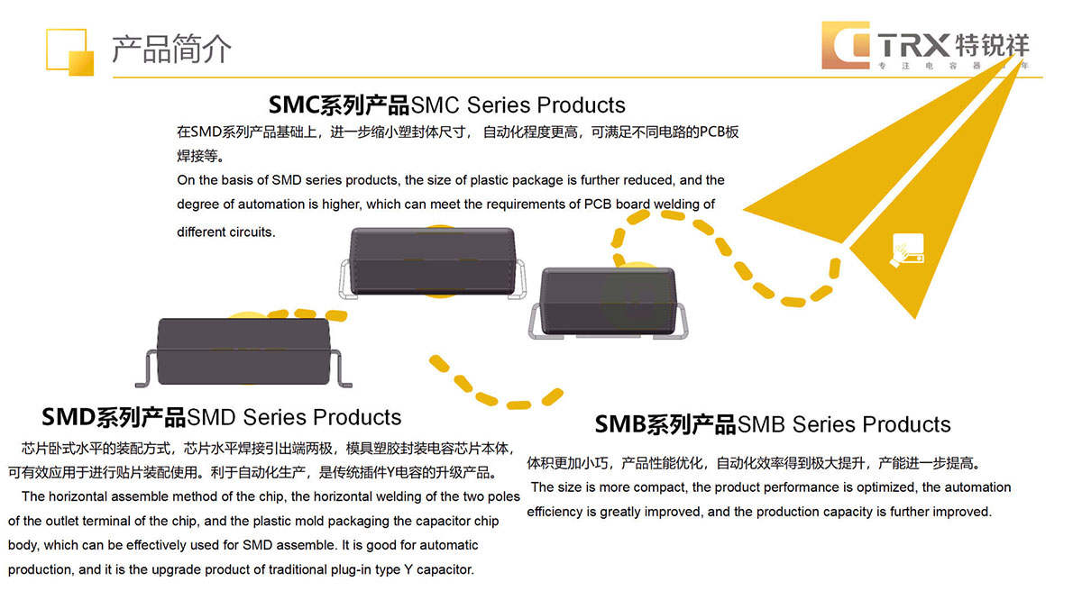
This is the introduction for TRX's products.
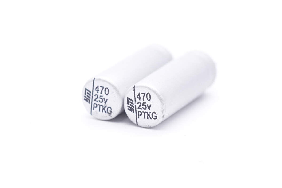
There're another two solid capacitors from Yongming NPT series. 470μF 25V for each.
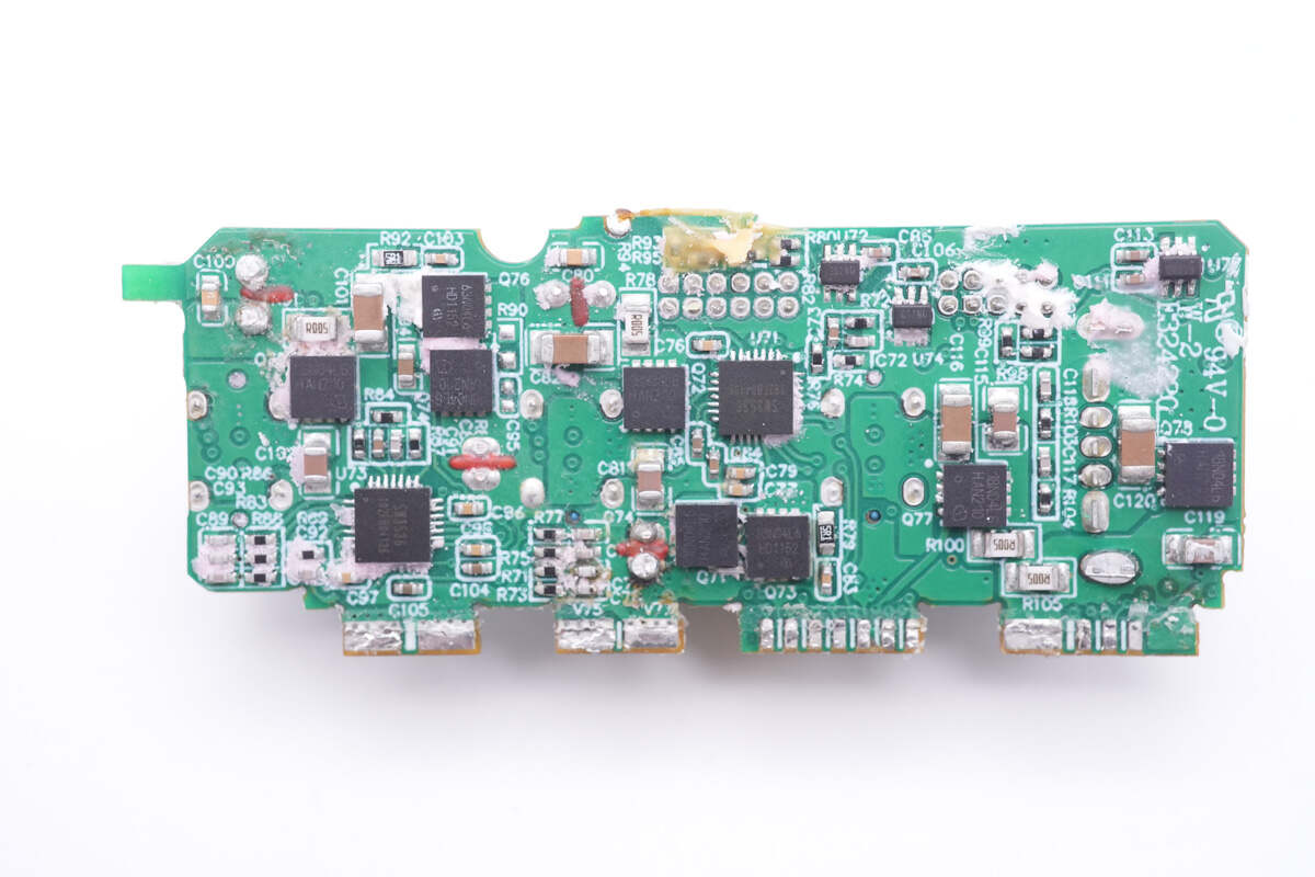
Then, let's move on to the secondary side. We found it has three output circuits for four output ports. The components of the three circuits are exactly the same, so we will take one of the circuits as an example.
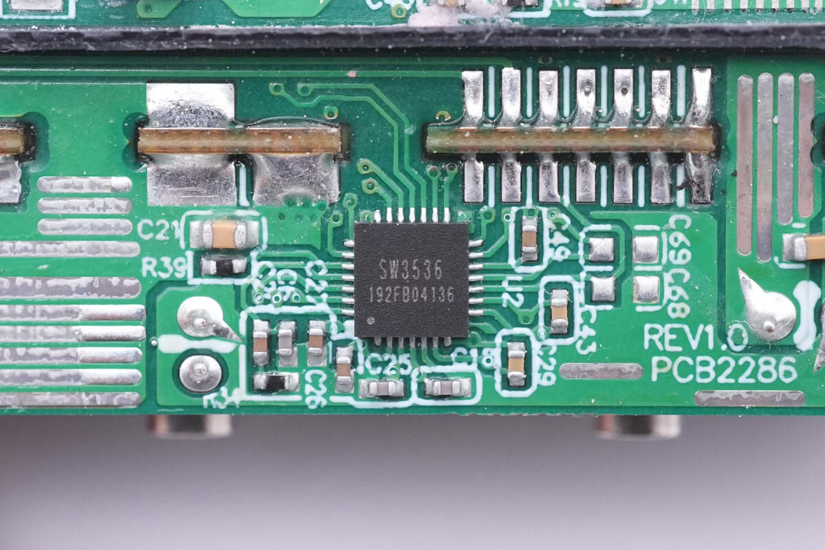
The protocol chip is from Ismartware. It supports multiple fast charging protocols such as PD, QC, PPS and supports a maximum output power of 140W. Model is SW3536.
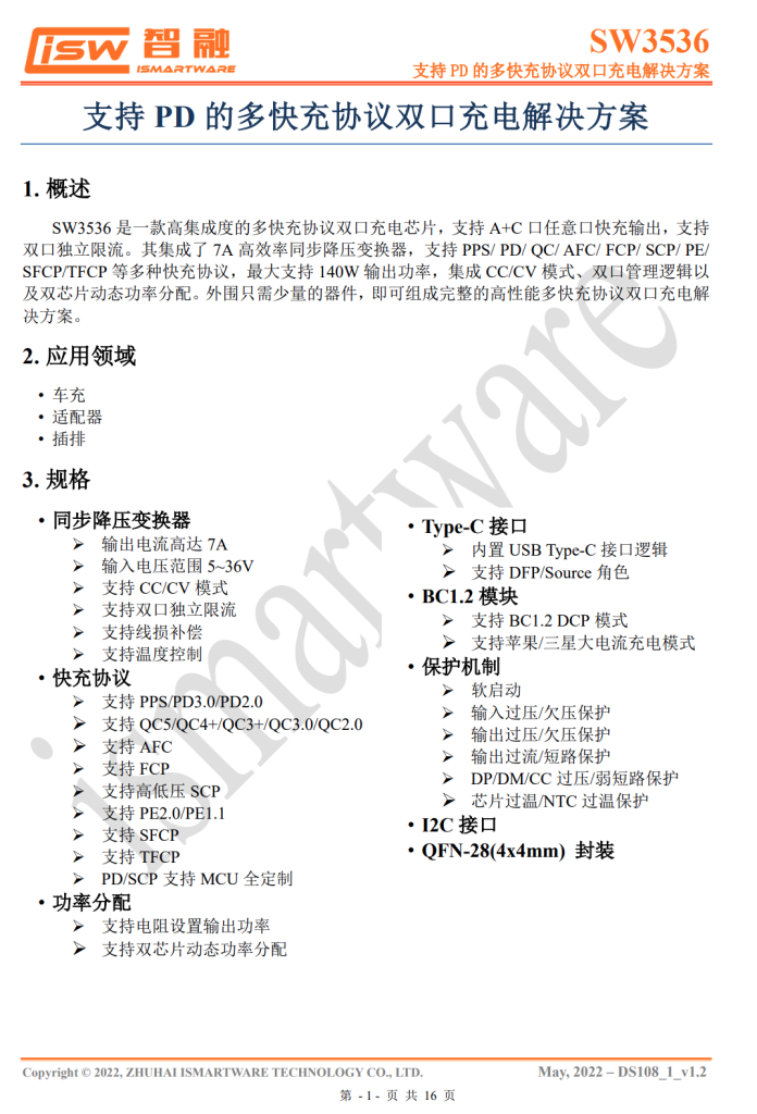
Here is all the information about SW3536.
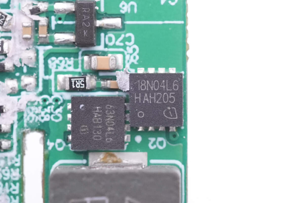
The first buck MOSFET is from Infineon. 40V, 1.8mΩ. Model is BSZ018N04LS6.
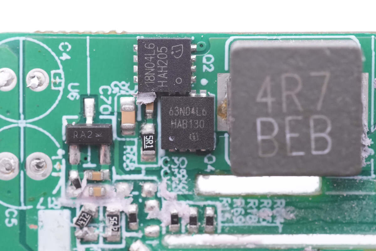
The second buck MOSFET is also from Infineon. 40V, 6.3mΩ. Model is BSZ063N04LS6.
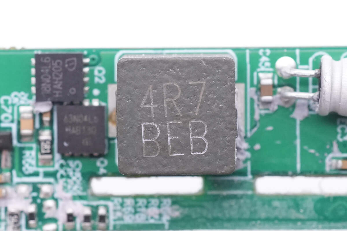
This is a 4.7μH alloy buck inductor.
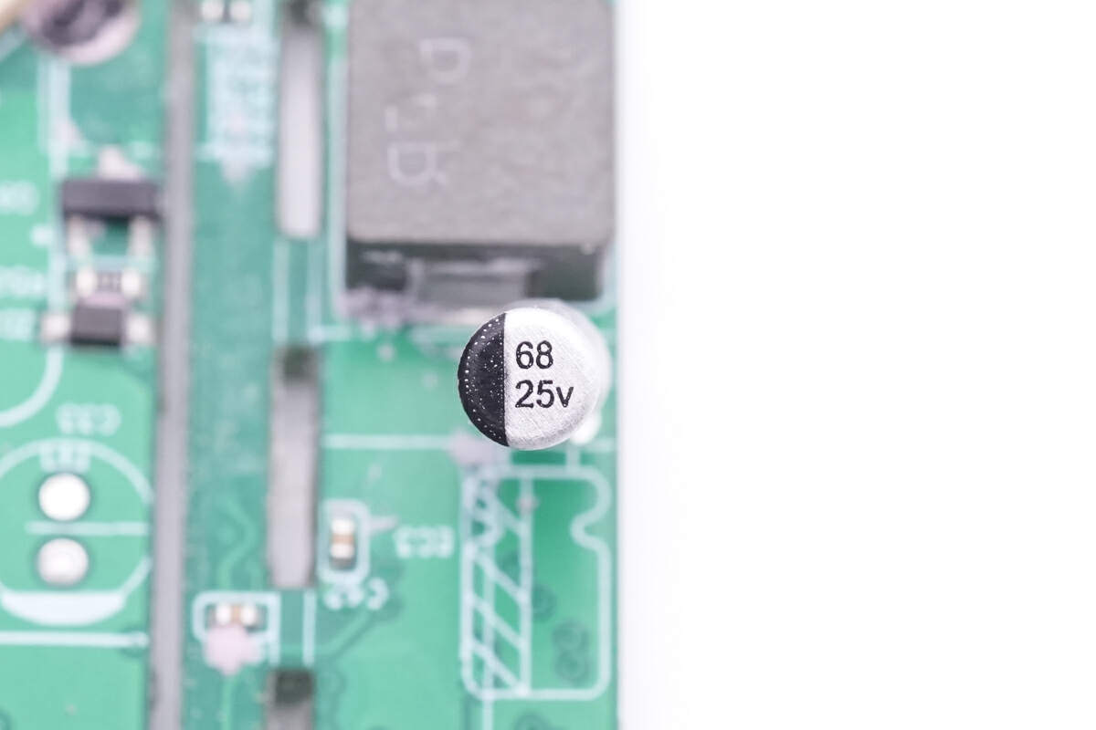
The buck solid capacitor is 68μF 25V.
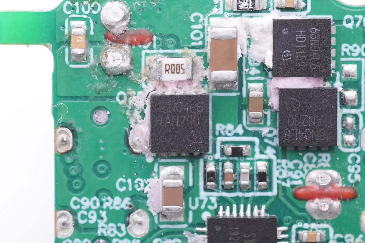
The output VBUS MOSFET is also from Infineon.
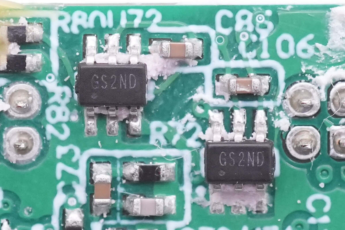
Except for those three output circuits, it also has four current sense amplifiers from SG-Micro for four output ports. Model is SGM8199A1.
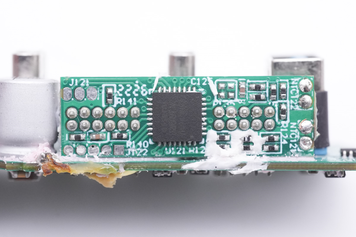
And there is another small PCB on here, with MCU chip and thermistors.
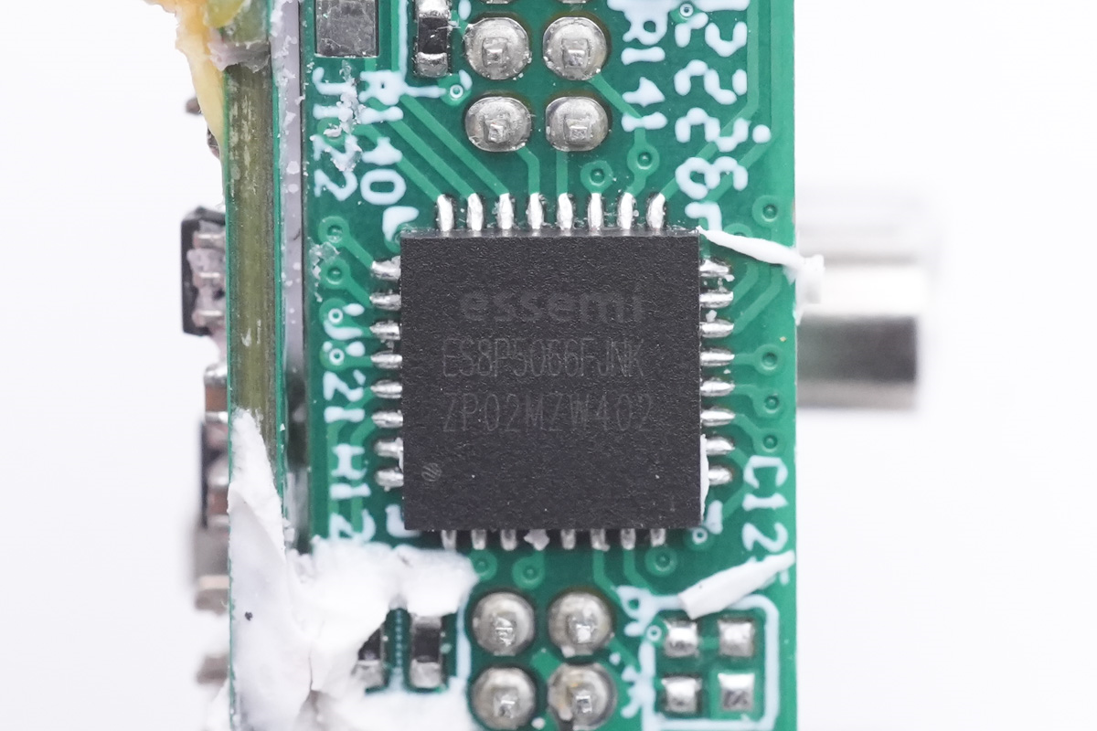
The 32-bit MCU from Eastsoft is soldered on that small PCB and adopts QFN32 package. It integrates an ADC and is used to detect internal temperature and protection. It can also distribute the output power of different ports. Model is ES8P5066FJNK.
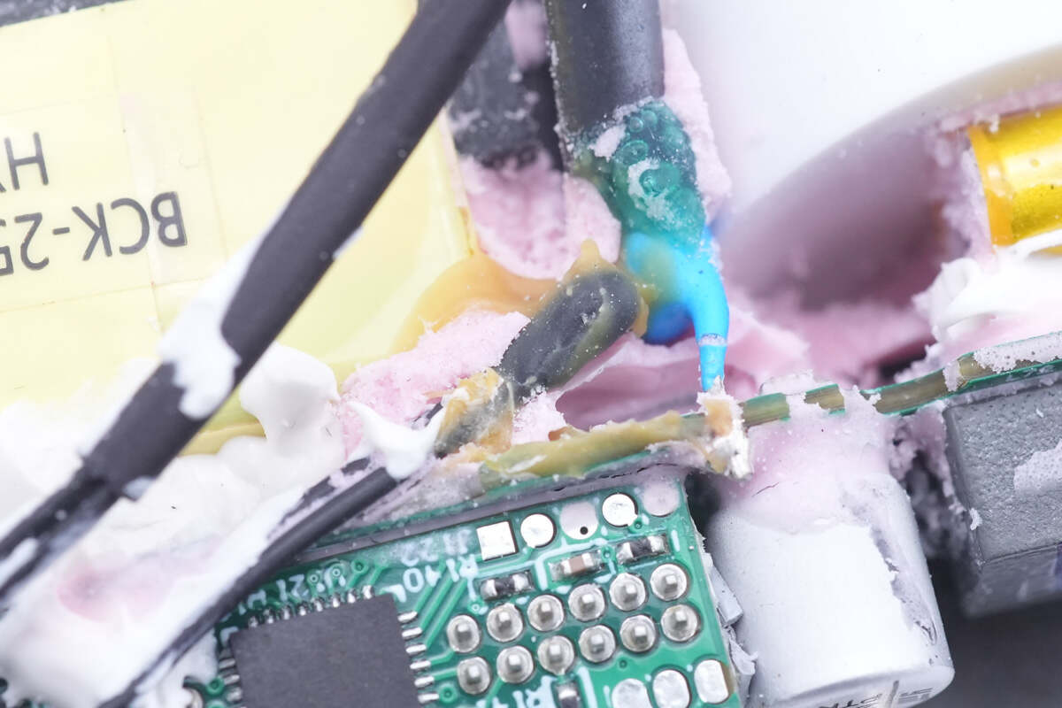
This thermistor we just mentioned can detect the temperature of the PFC boost inductor.

And this one is for planar transformer..
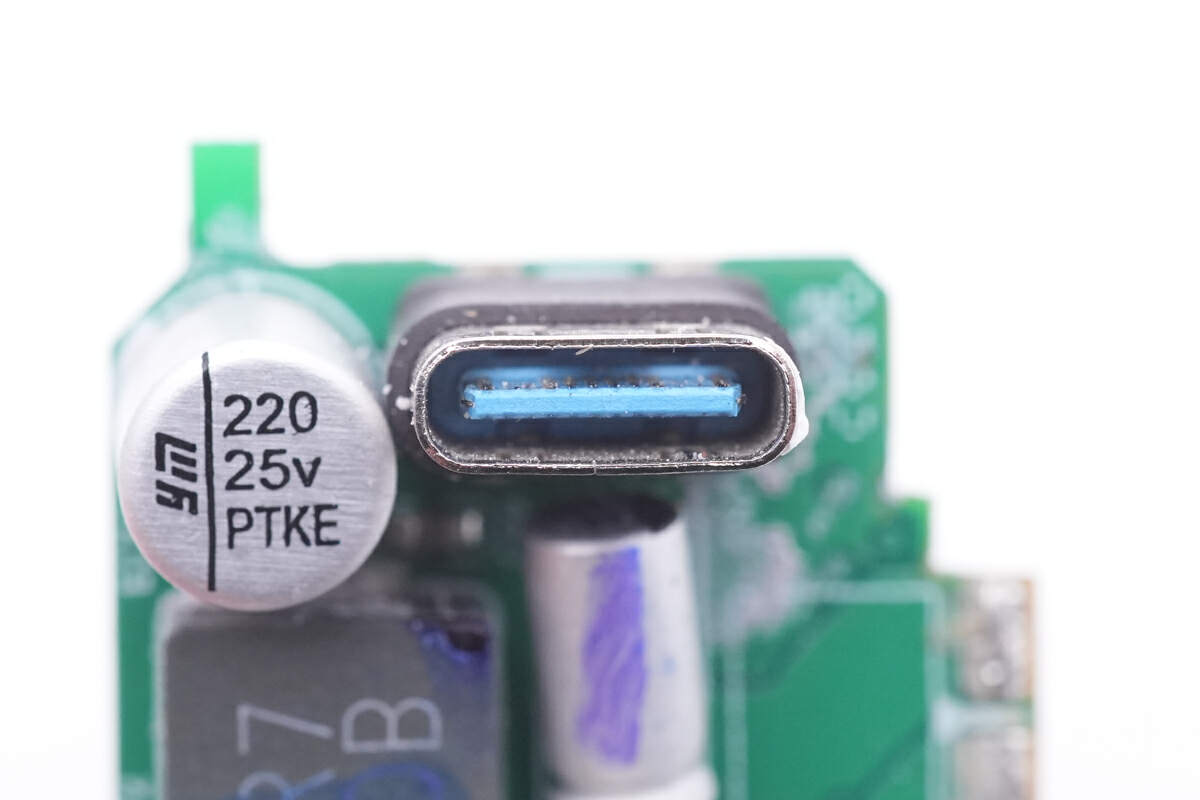
The plastic sheet inside the USB-C sockets is blue.
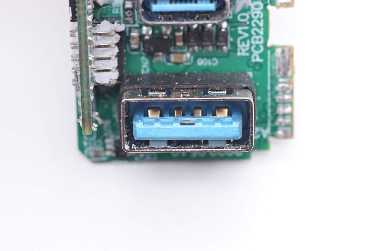
So is the USB-A.
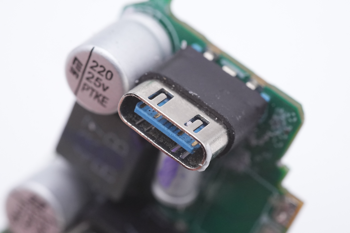
They are sealed with heat shrink tubing at the bottom.
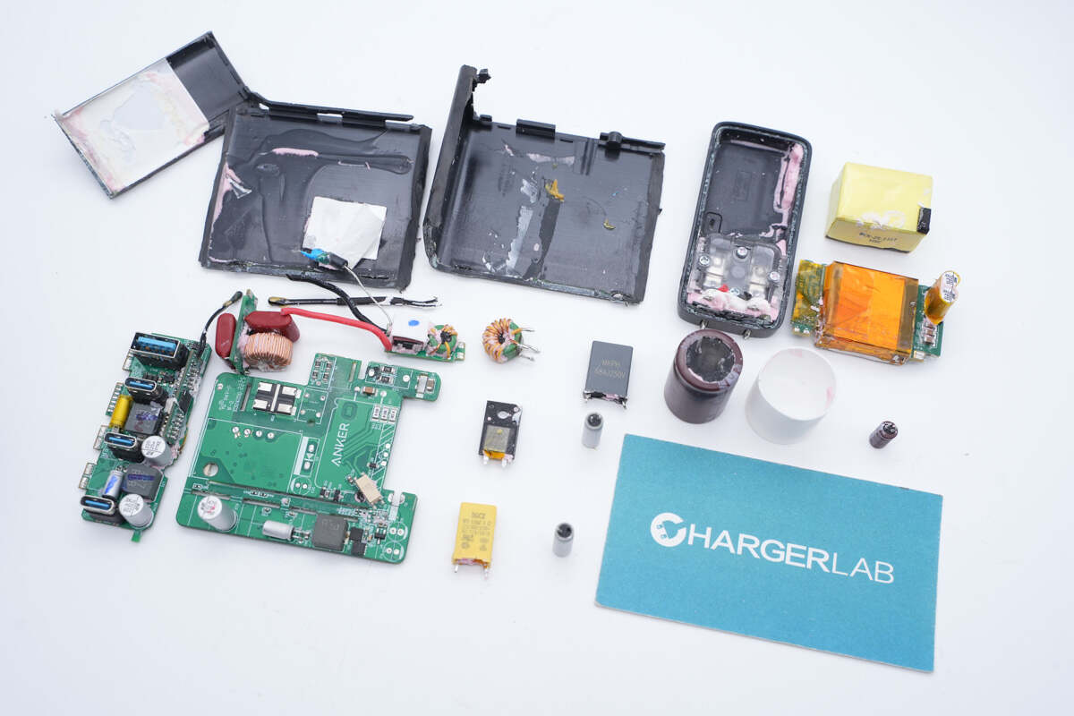
Well, that's all components of this 150W GaN Charger from Anker.
Summary of ChargerLAB
After taking it apart, we found that it still has the consistent high-quality of the GaNPrime series and integrates multiple Infineon GaN ICs. The stackable PCB design and planar transformer make it even smaller. Four USB ports are controlled by three buck circuits, and the components of each circuit are the same. So, all USB-C port scan reach 100W and supports dynamic power distribution.

