Introduction
Recently, ChargerLAB got a super-performance GaN charger, A2655, launched by the well-known brand ANKER. The product is now available on the Apple Store. It has four USB-C output ports, and the USB-C1 port supports 140W PD3.1, and the other three ports also support an output power of 100W.
Not only that, the total output power of multiple ports can reach 150W, which can meet the simultaneous fast charging needs of multiple devices such as MacBook, iPad, iPhone, Apple Watch, etc. Next, let's take it apart to see its internal components and structure.
Product Appearance
ANKER, product appearance, name, and selling points are printed on the front of the box.
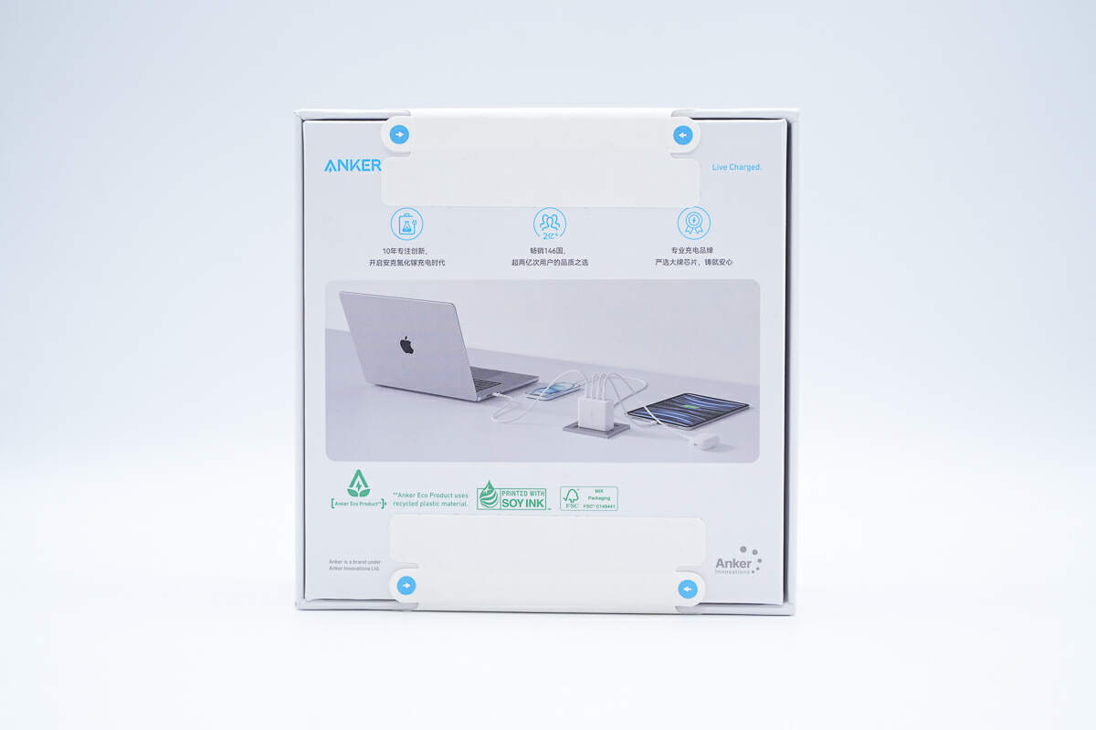
The back is also printed with selling points and application scenarios for charging laptops, phones, and headphones at the same time.
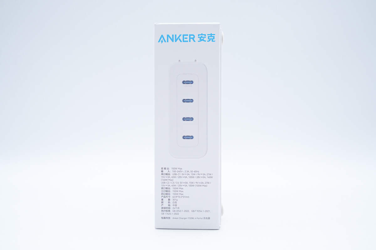
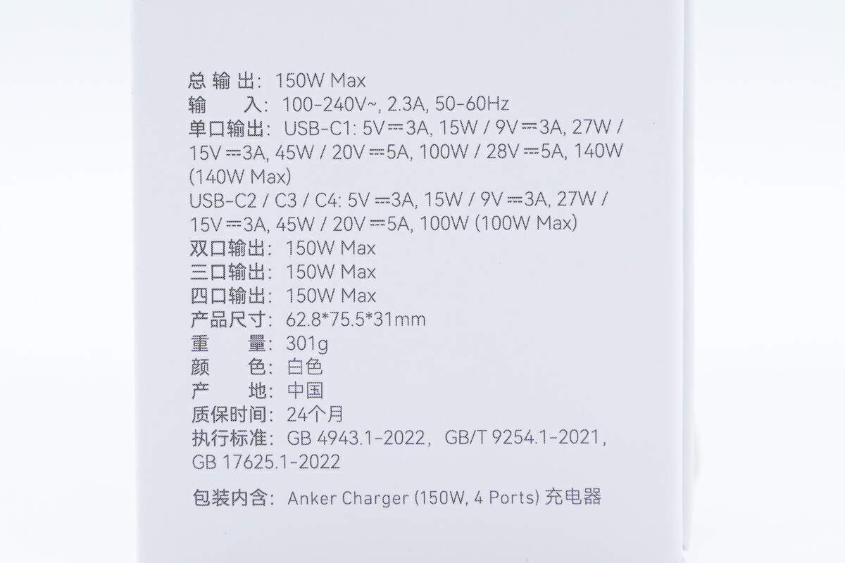
The specs info is printed on the side.
We'll talk about it later.
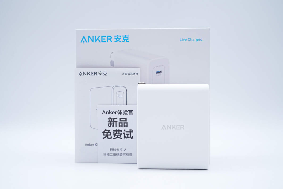
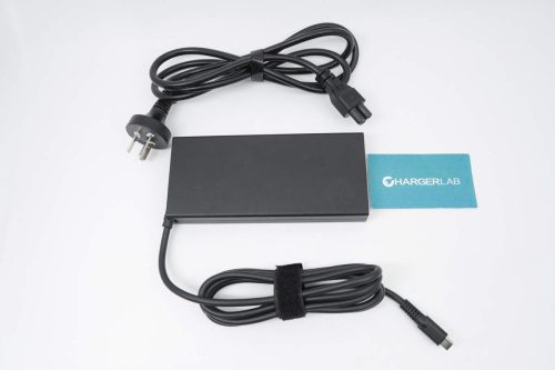
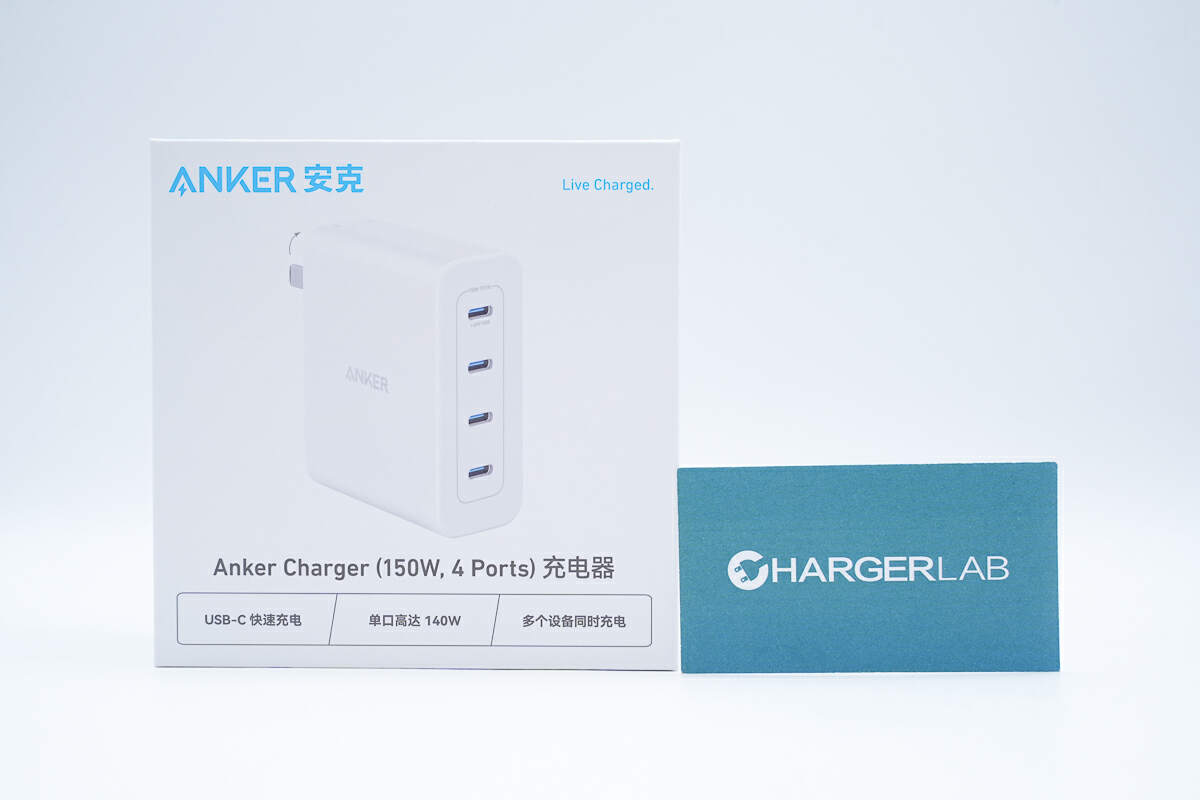
The box contains the charger and some documents.
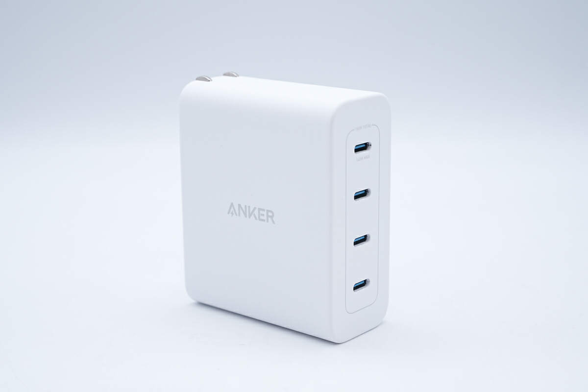
The shell is made of white PC flame-retardant material with a matte surface treatment, which feels delicate and is anti-fingerprint.
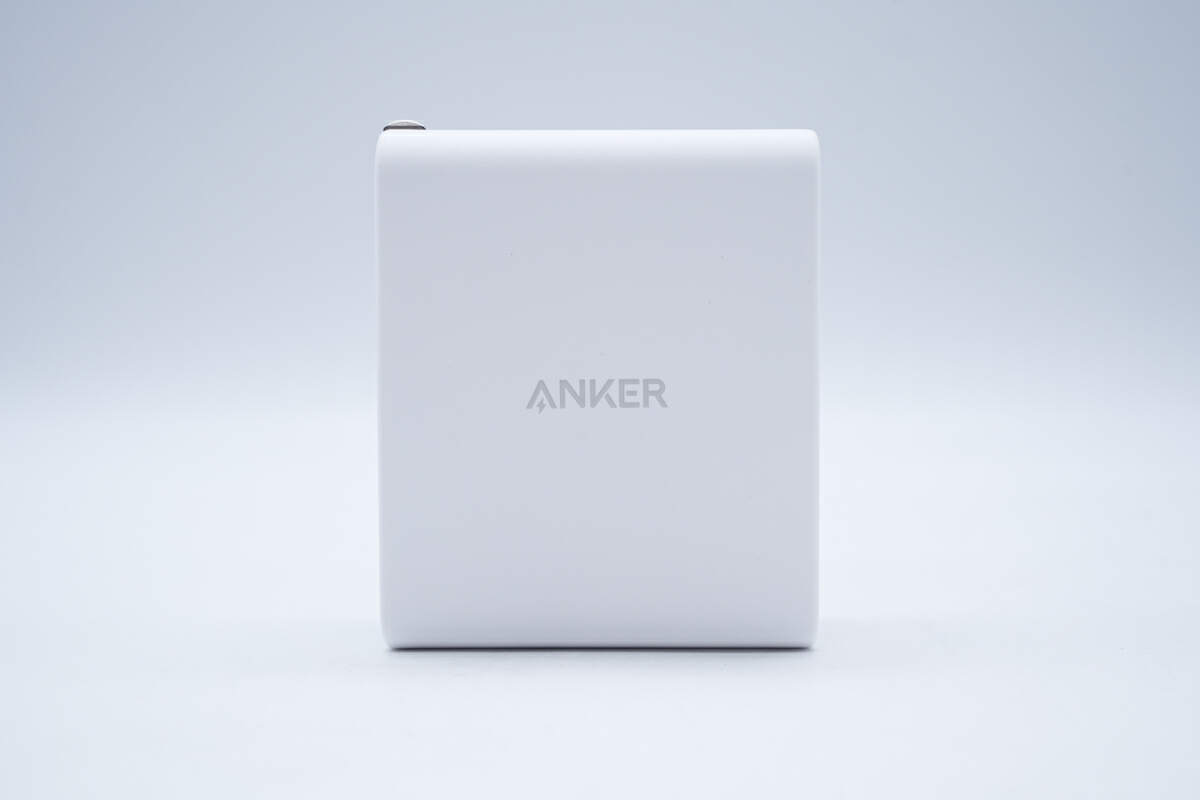
ANKER is printed on the front center.
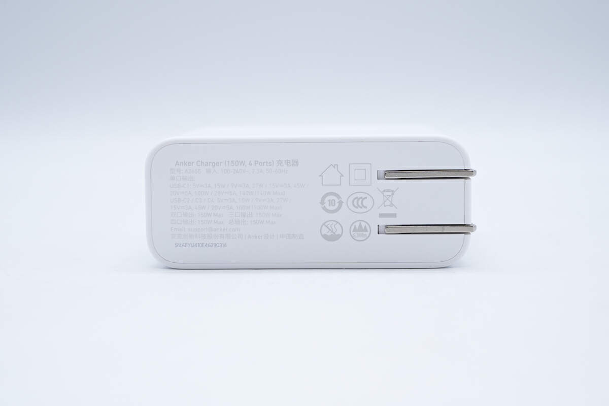
The spec info is printed on the input panel.
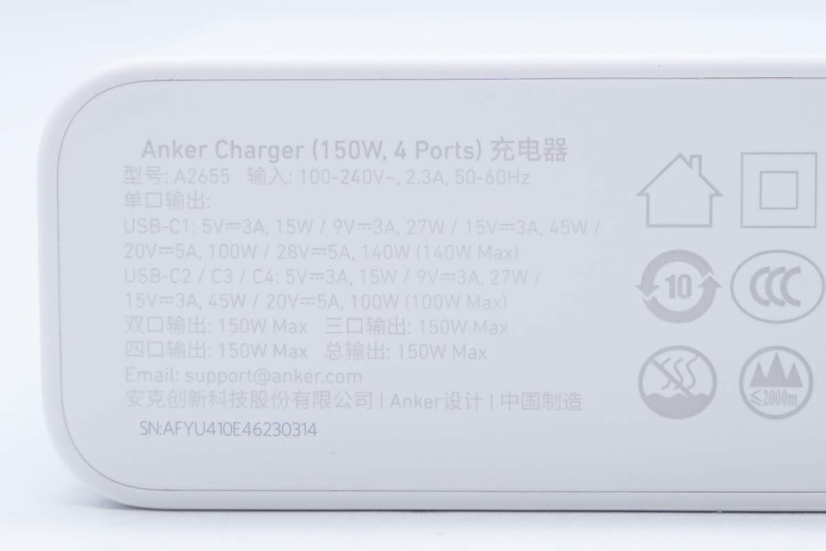
Model is A2655. It can support input of 100-240V~50/60Hz 2.3A. The USB-C1 can support output of 5V3A, 9V3A, 15V3A, 20V5A, and 28V5A, 140W Max. The USB-C2/C3/C4 can support 5V3A, 9V3A, 15V3A, and 20V5A, 100W Max. The maximum output power is 150W.
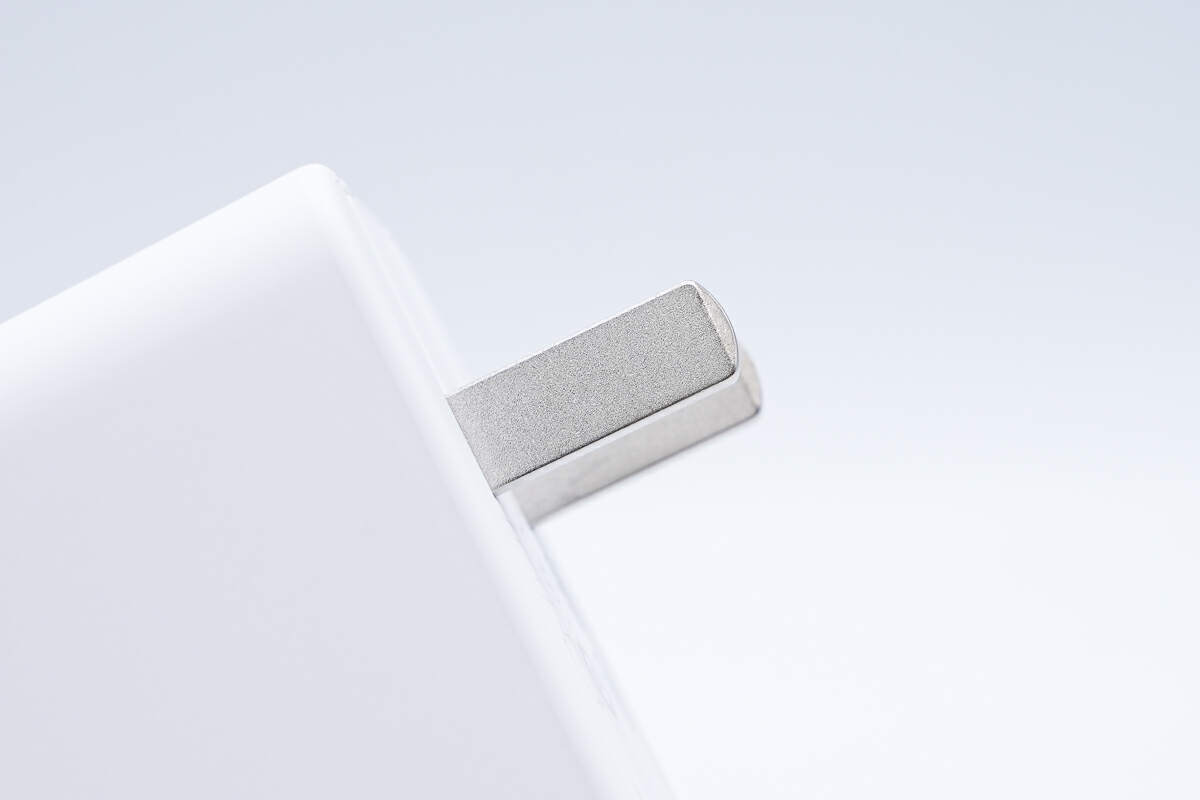
It comes with a foldable plug.
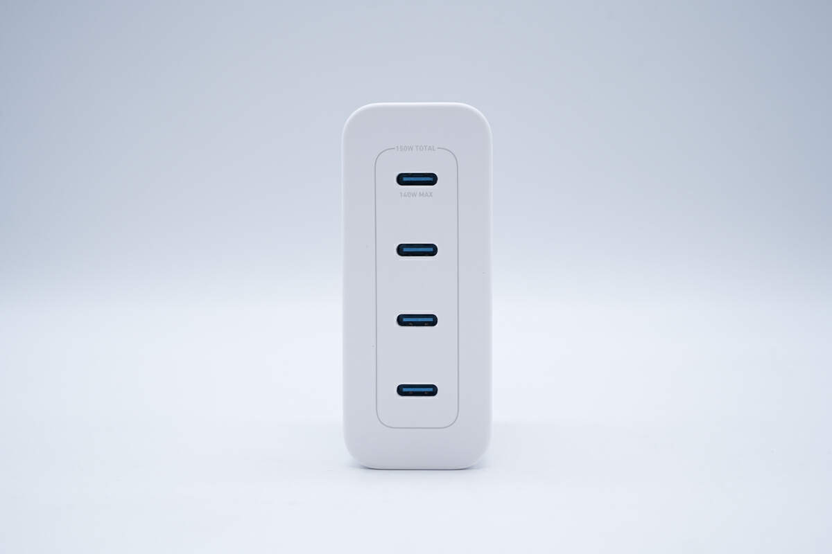
The plastic sheets of the four USB-C ports are all blue.
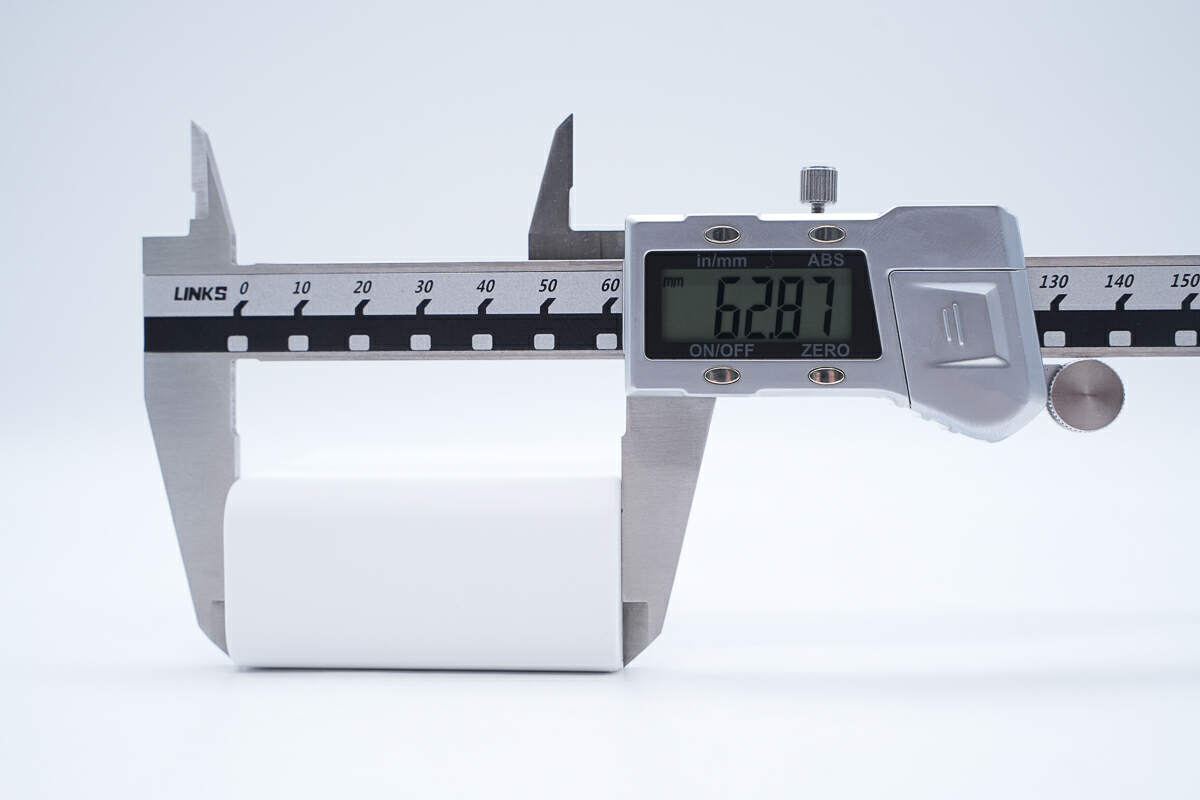
The length is about 62.87 mm (2.48 inches).
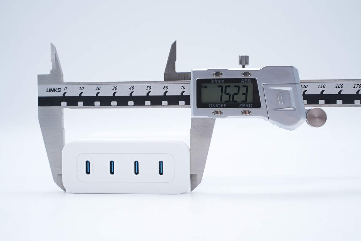
The width is about 75.23 mm (2.96 inches).
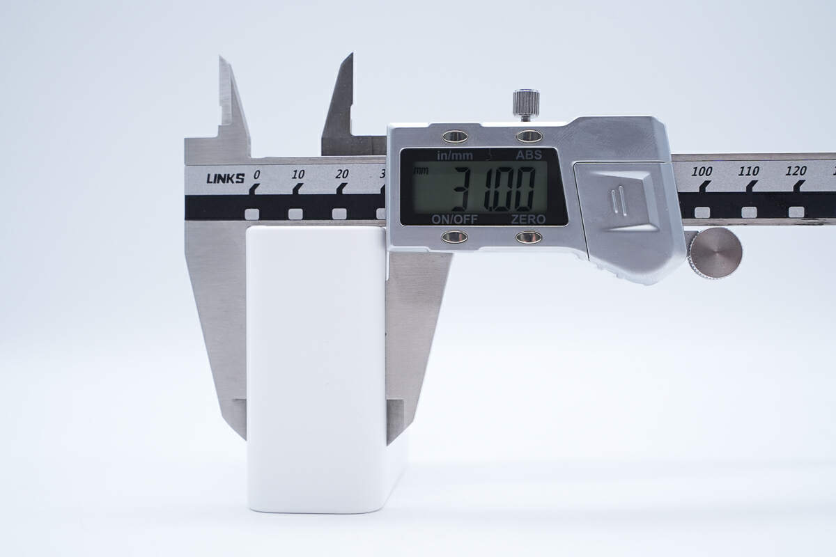
The thickness is about 31 mm (1.22 inches).
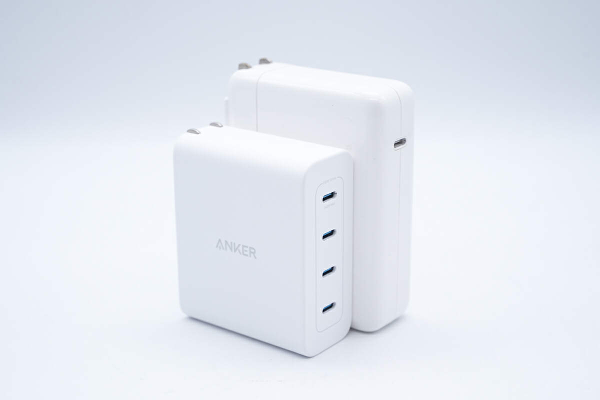
Compared with the Apple 140W charger, it has an obvious size advantage.
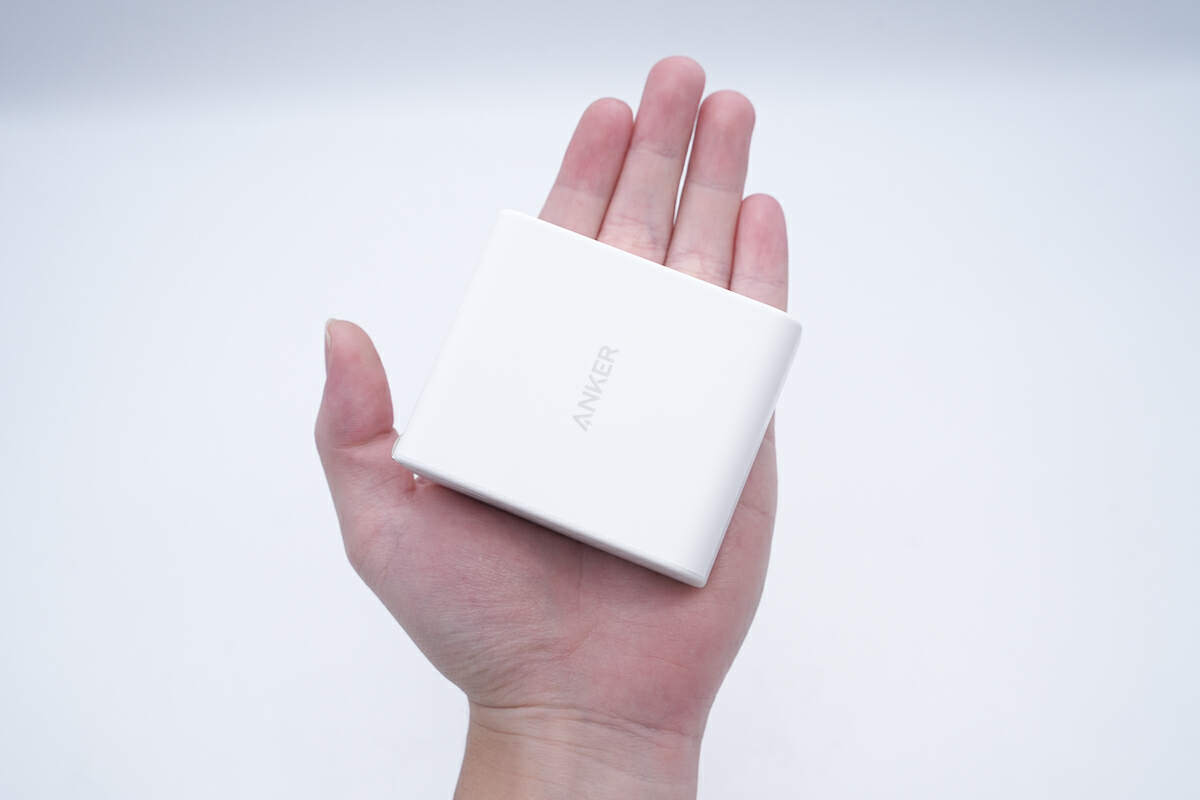
That's how big it is in the hand.
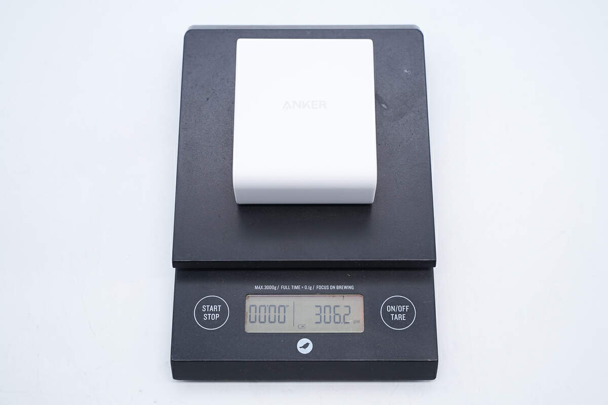
The weight is about 306 g (10.79 oz).
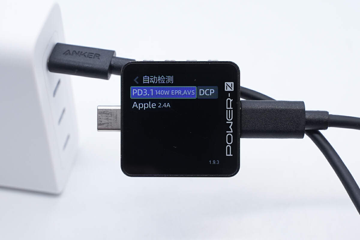
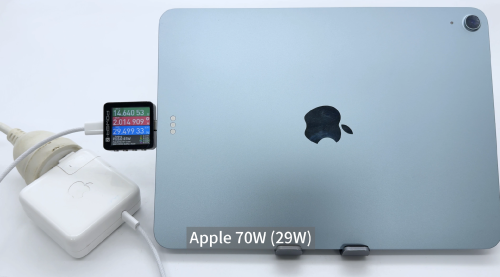
ChargerLAB POWER-Z KM003C shows the USB-C1 can support PD3.1, DCP, and Apple 2.4A charging protocols.
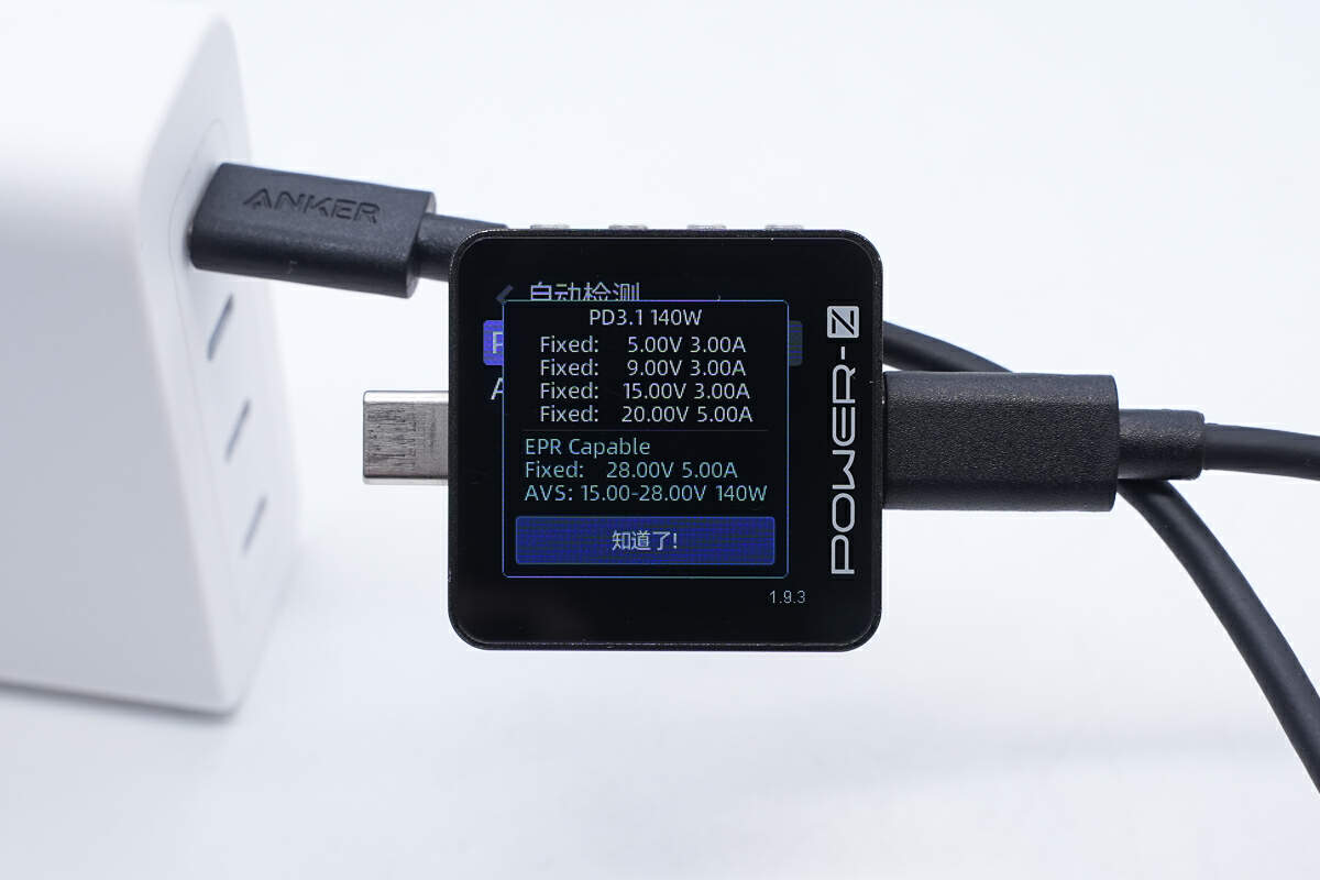
And it has five fixed PDOs of 5V3A, 9V3A, 15V3A, 20V5A, and 28V5A. It also has a set of AVS, which is 15-28V 140W.
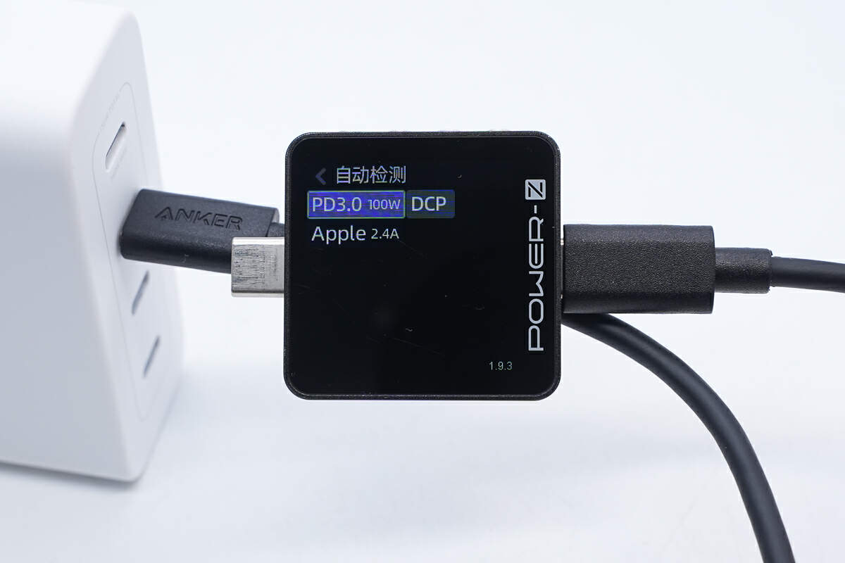
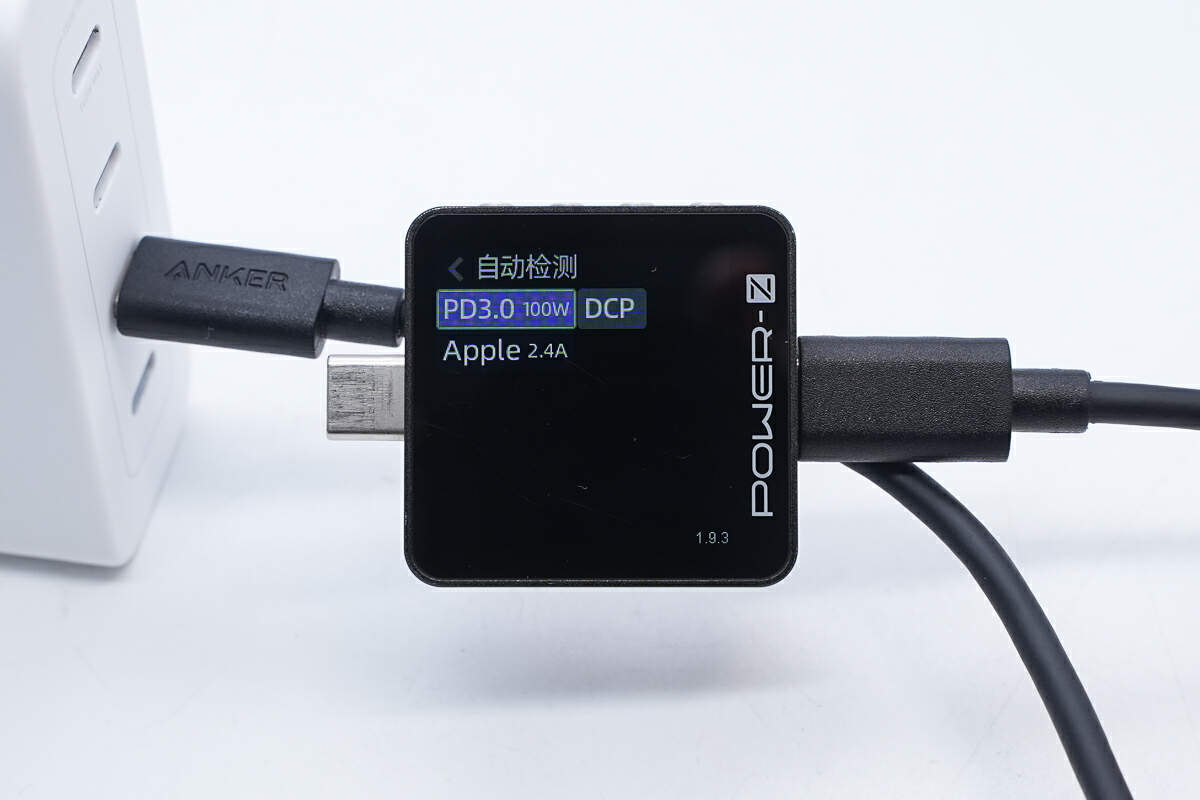
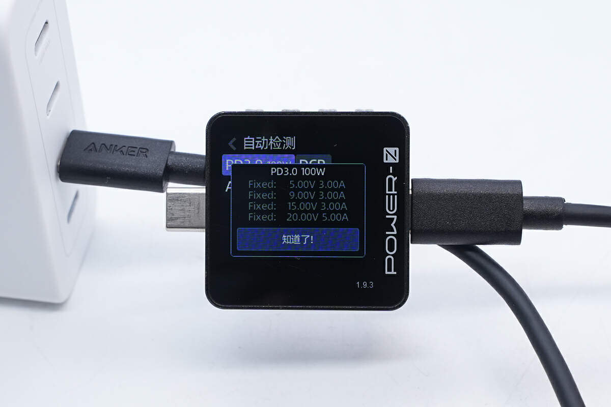
ChargerLAB POWER-Z KM003C shows the USB-C2 can support PD3.0, DCP, and Apple 2.4A charging protocols.
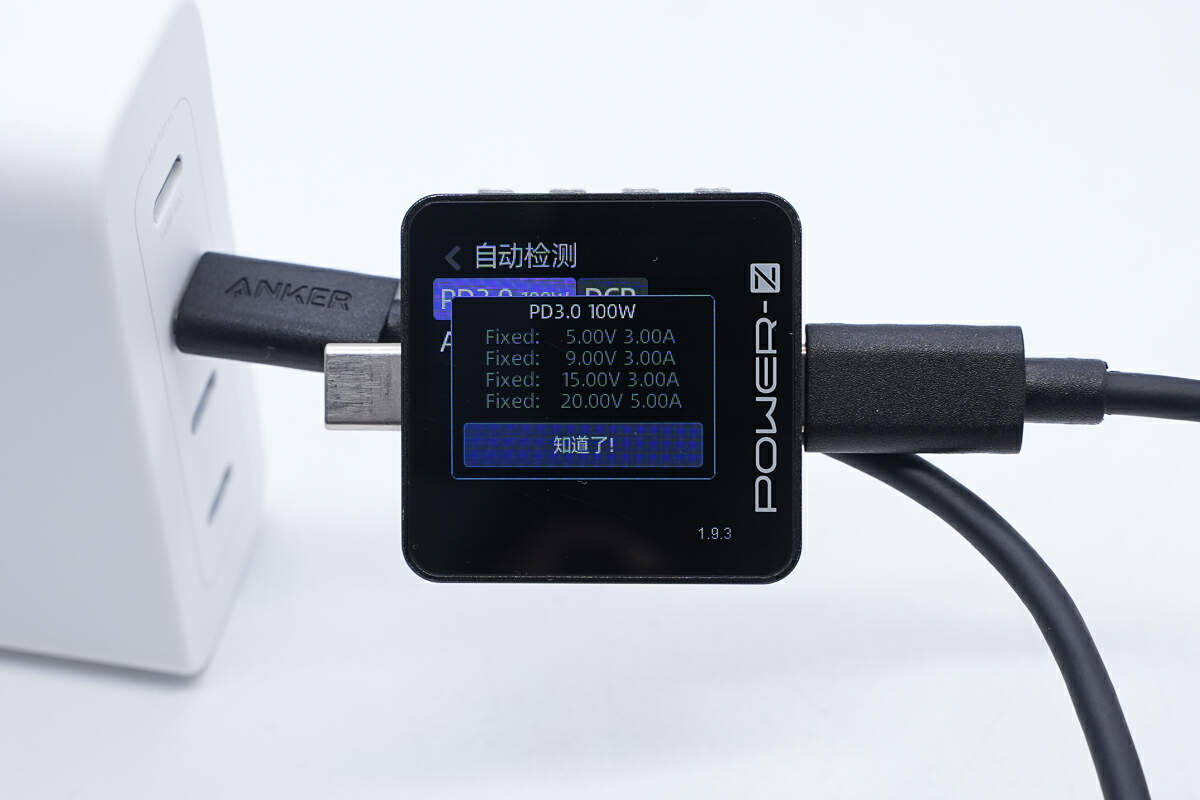
And it has four fixed PDOs of 5V3A, 9V3A, 15V3A, and 20V5A.
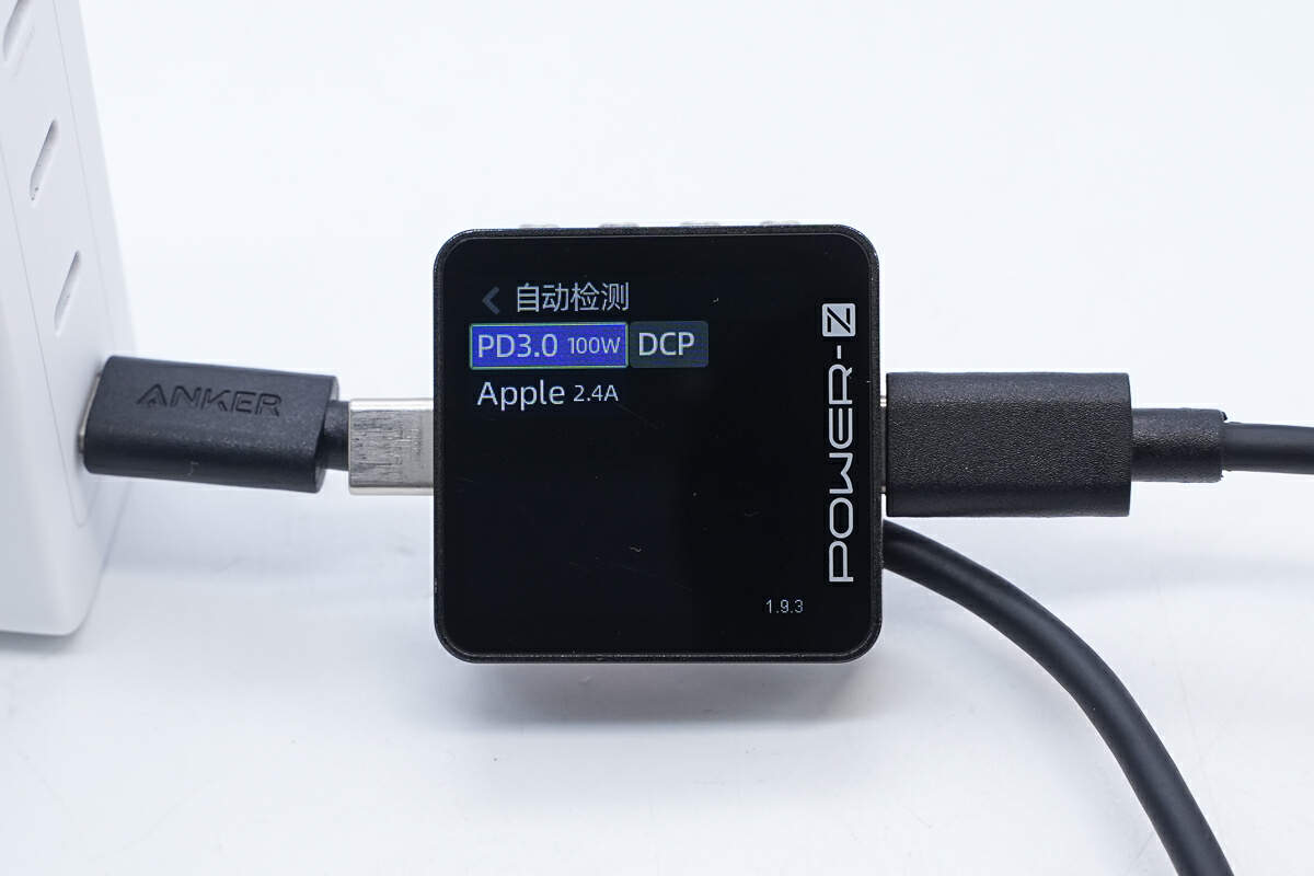
The protocols compatible with USB-C3 are the same as those of USB-C2.
So as the PDOs.
It is measured that the compatible protocols of the USB-C4 port are the same as those of the previous two ports.
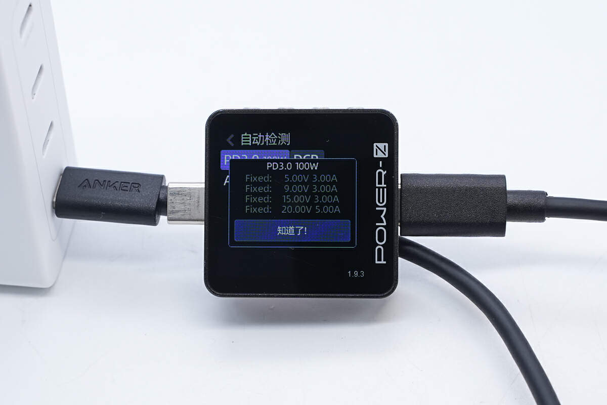
So as the PDOs. The performance of USB-C2, USB-C3, and USB-C4 ports is the same.
Teardown
Next, let's take it apart to see its internal components and structure.
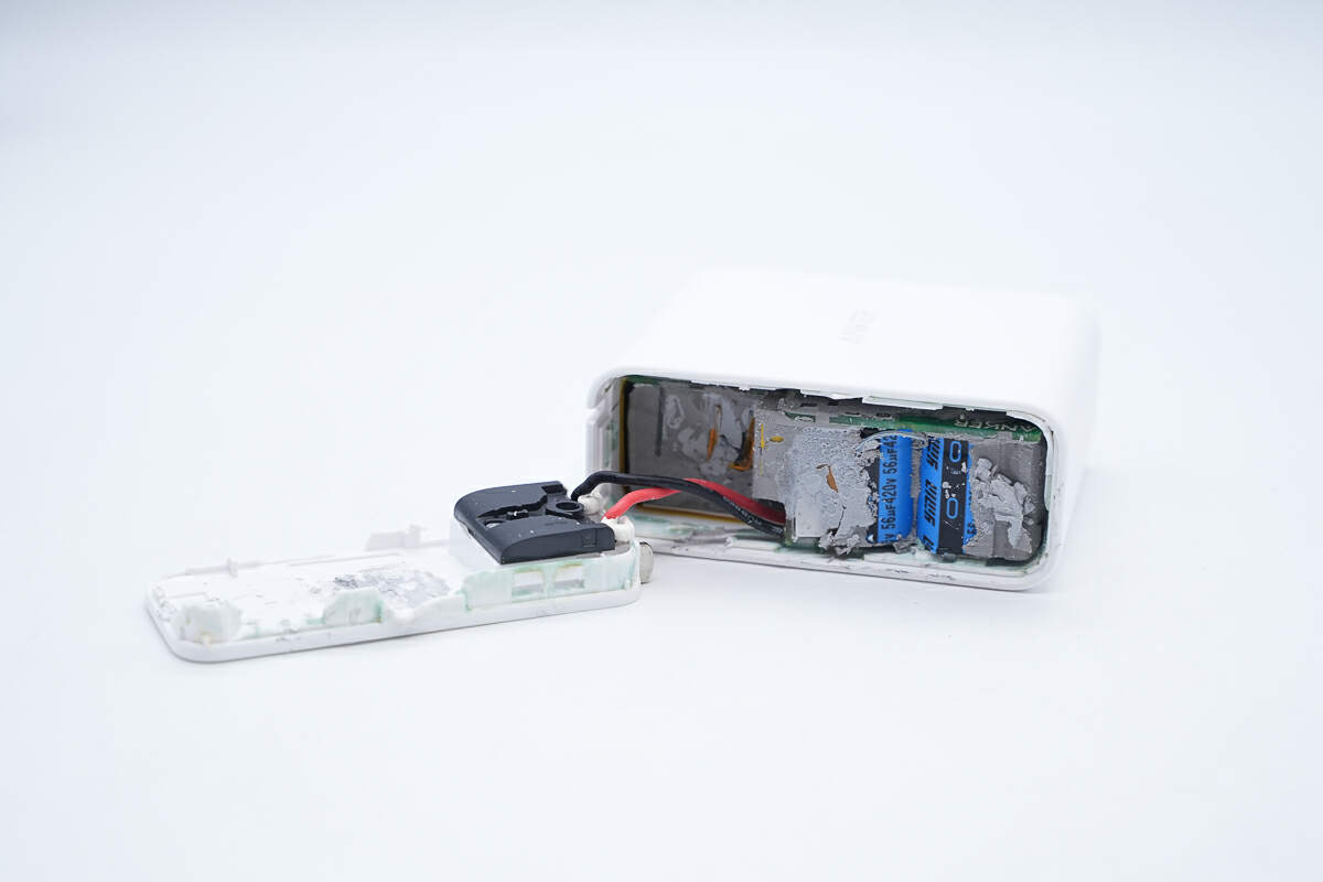
Remove the input end shell, the shell is ultrasonically welded, and the plug is fixed with a black plastic shell and screws.
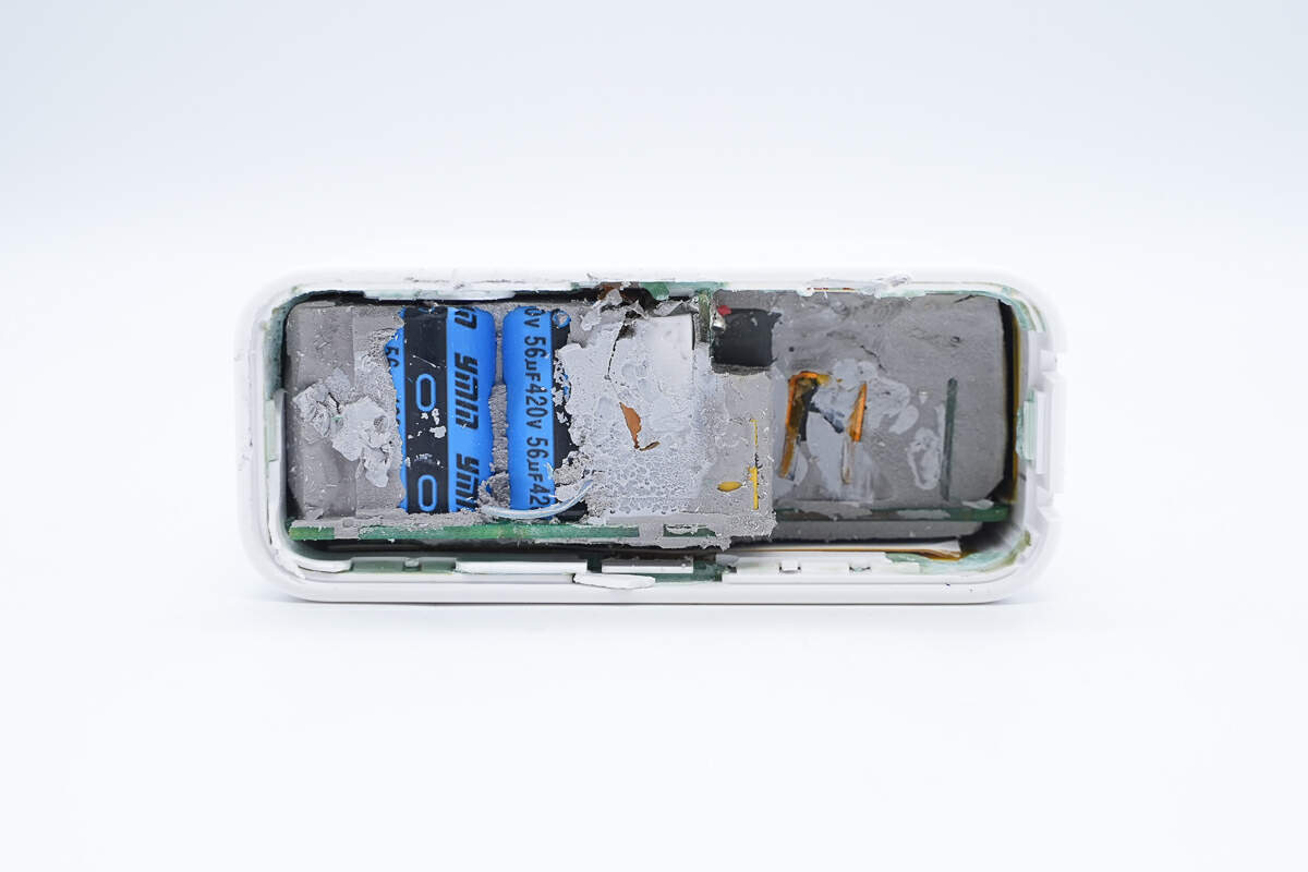
The interior of the charger is filled with potting compound to improve heat dissipation.
Take out the PCBA module. There are copper plates and aluminum foils stuck on the inside of the case to help dissipate heat. At the same time, high-temperature-resistant insulating tape is also attached.
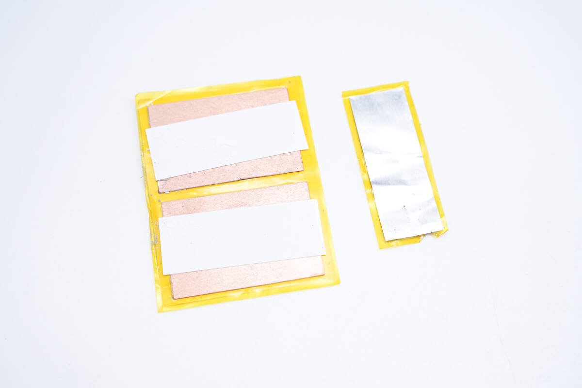
There are copper plates and aluminum foils.
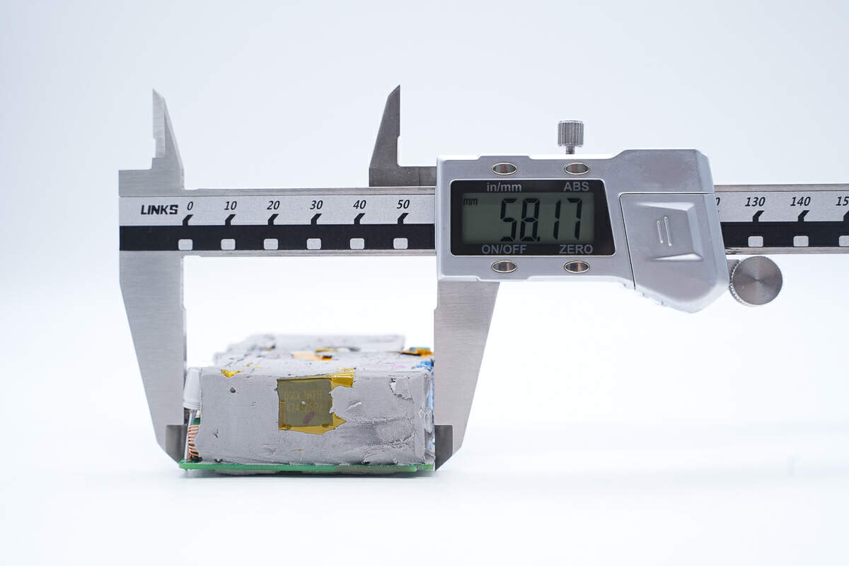
The length of the PCBA module is about 58.17 mm (2.29 inches).
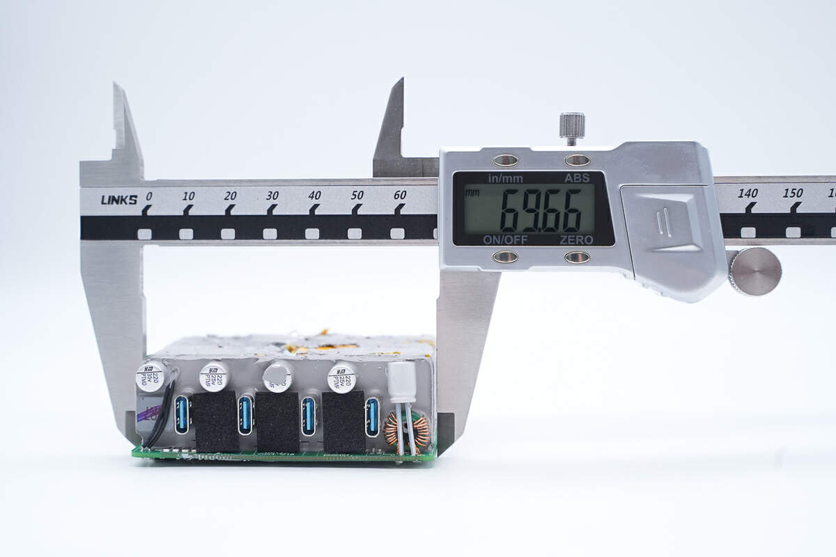
The width is about 69.66 mm (2.74 inches).
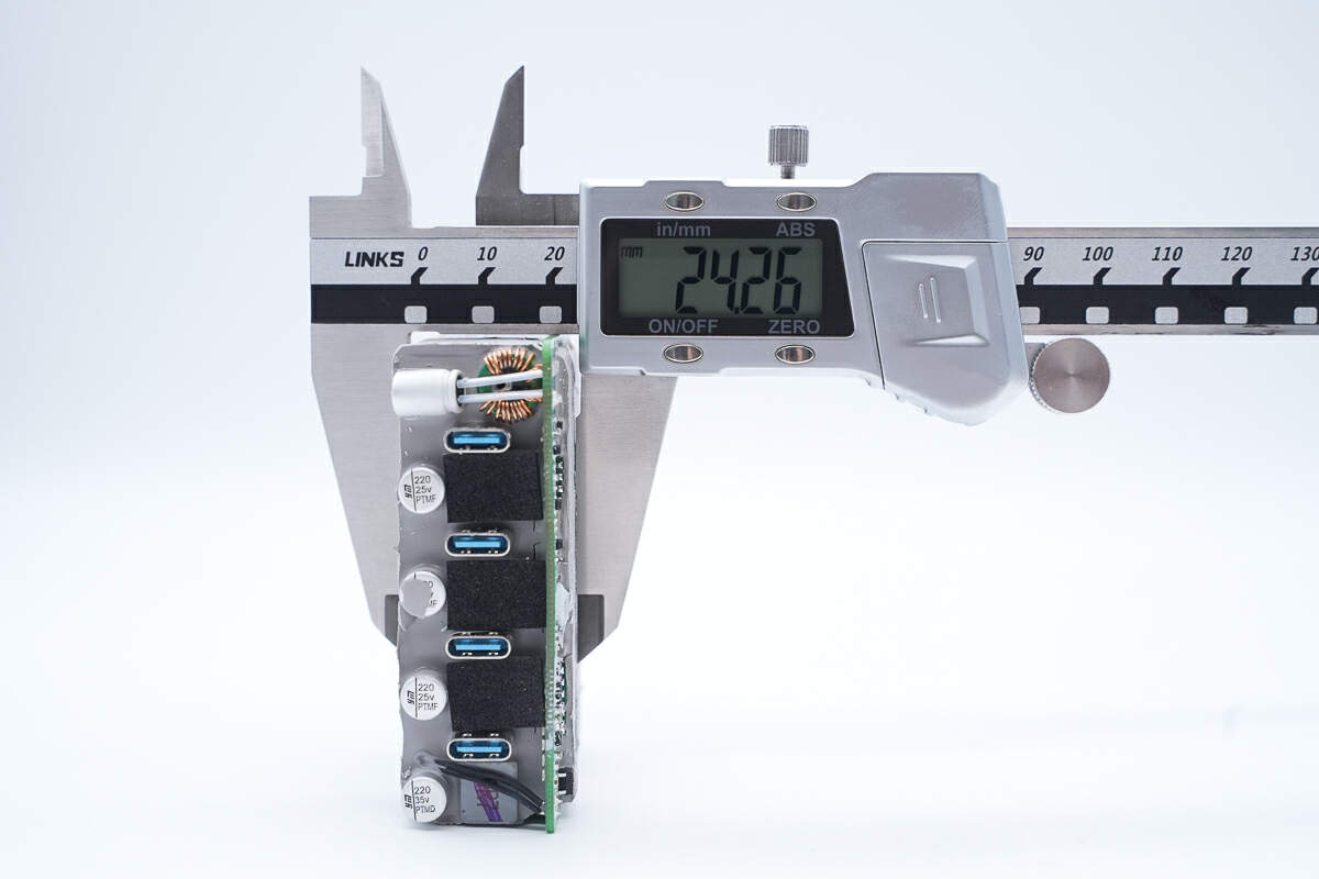
The thickness is about 24.26 mm (0.96 inches).
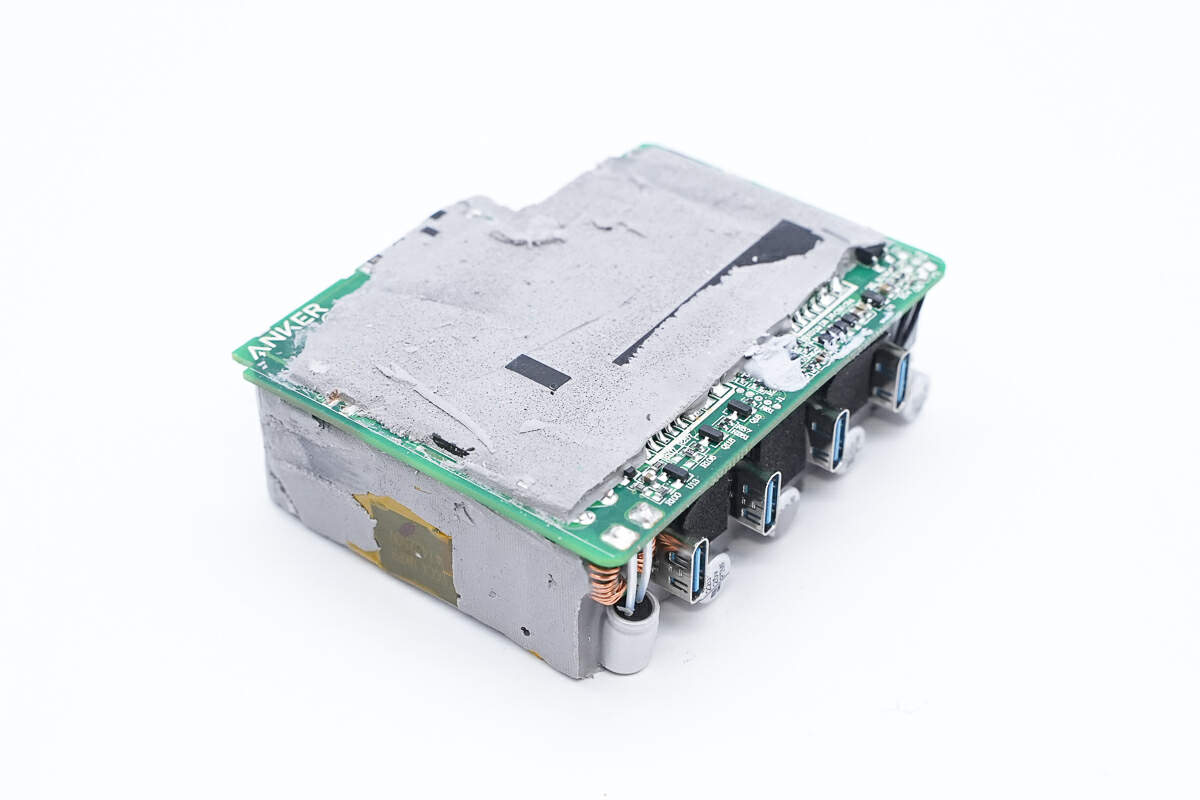
The front and back sides of the PCBA module are covered with gray potting compounds.
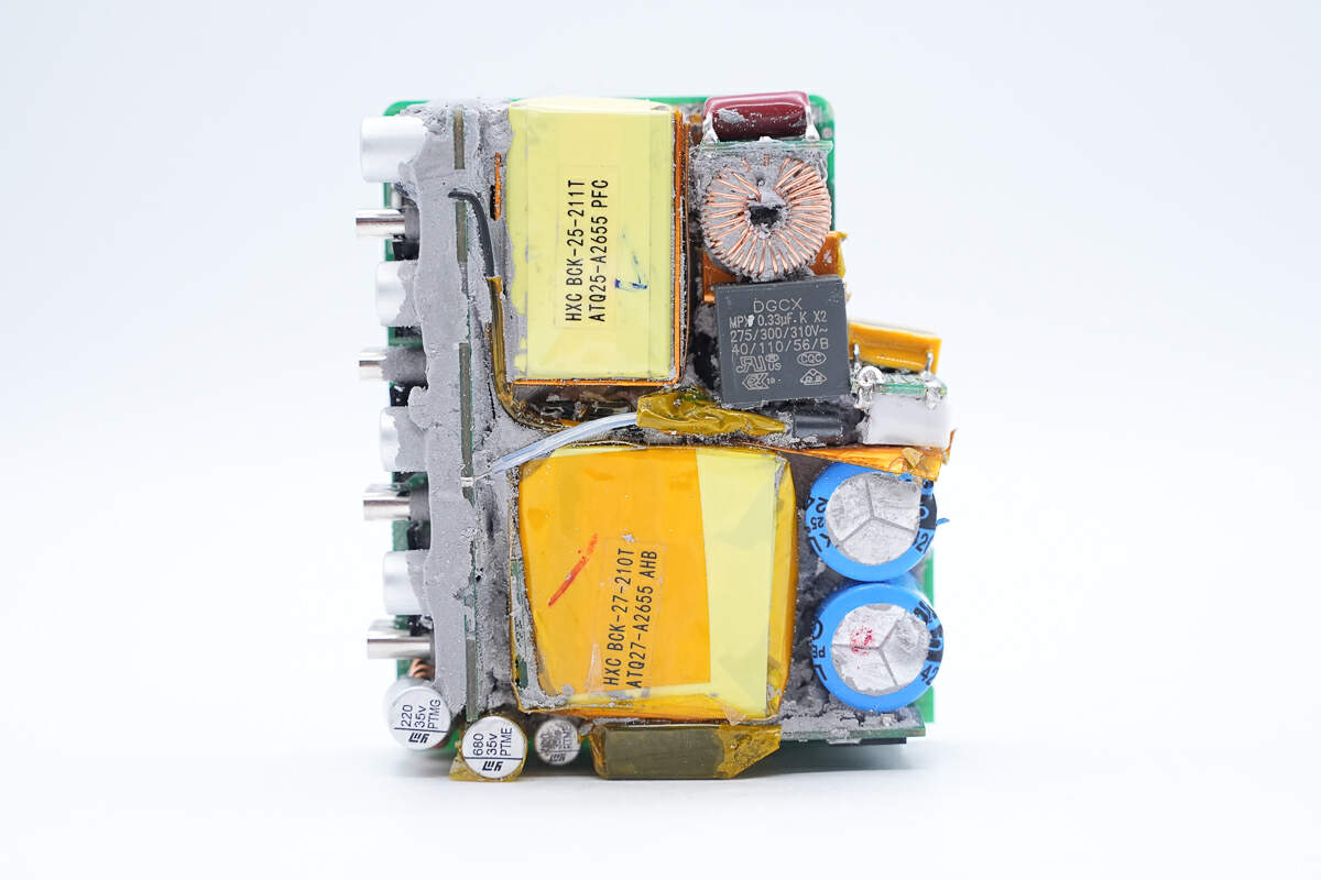
After cleaning up the potting compound, the components on the front of the PCBA are very compactly arranged. The PFC boost inductor is also covered with a heat sink, and the transformer, capacitors, and other components are all wrapped with insulating tape.
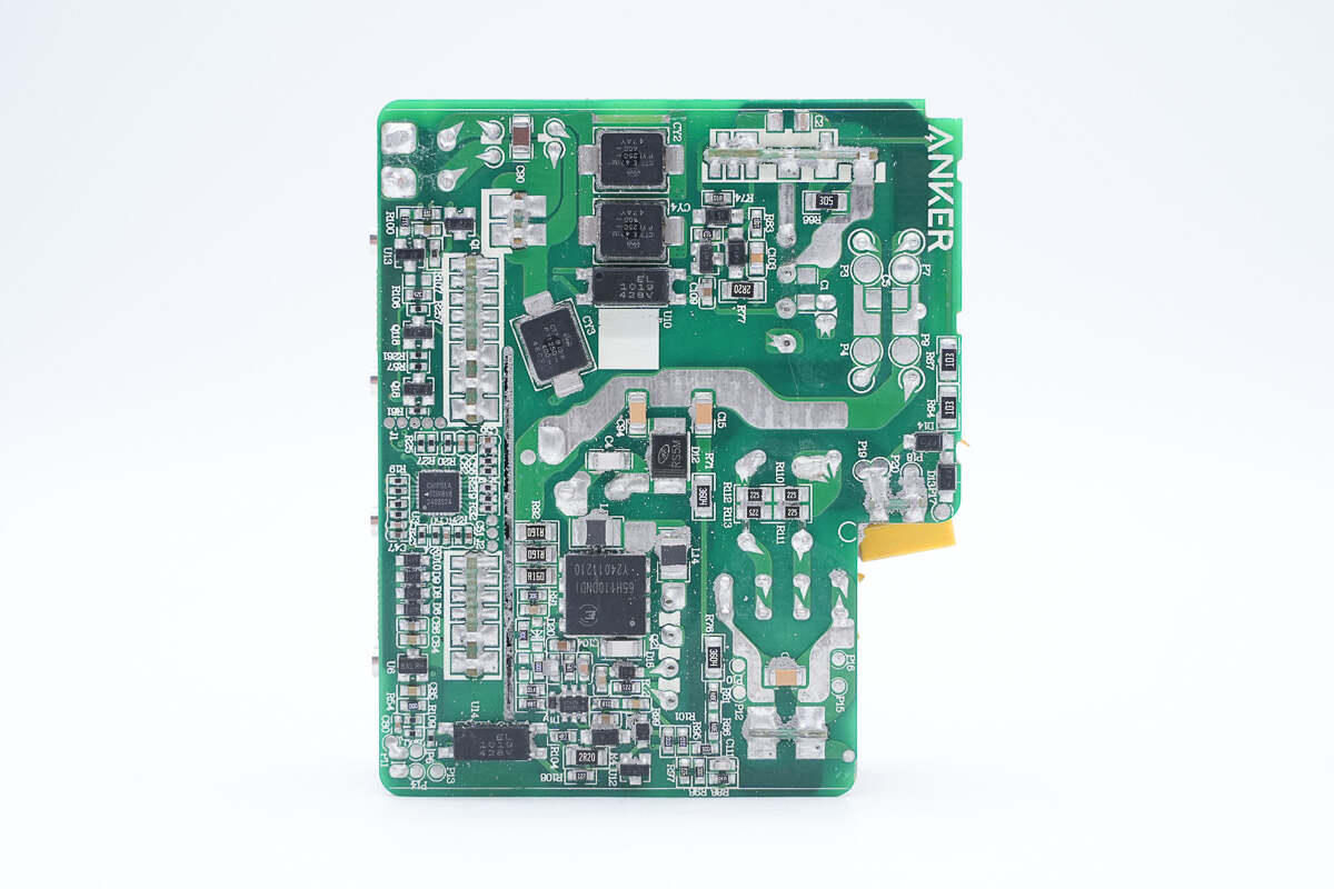
The back of the PCBA is equipped with a PFC controller, PFC MOSFET, optocoupler, SMD Y capacitor, and MCU.
There are three small PCBs at the input end of the PCBA module. The small PCB in the middle is equipped with a time delay fuse, common mode choke, and safety X2 capacitor. The left area has high-voltage filter electrolytic capacitors, and the right side has another common mode choke, safety X2 capacitor, and two bridge rectifiers.
Remove the small PCB at the input end and find the time delay fuse on the front covered with a white rubber sleeve for insulation protection.
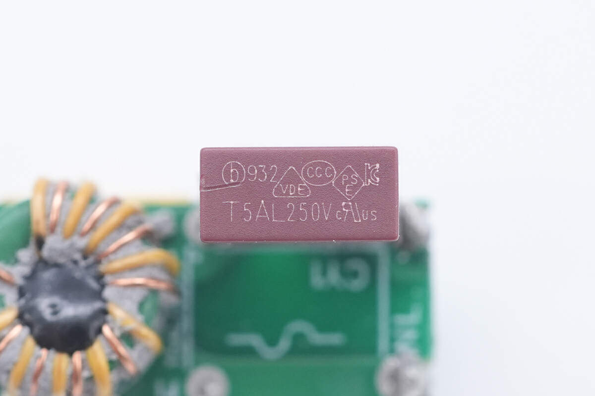
The time delay fuse is from Betterfuse. 5A 250V.
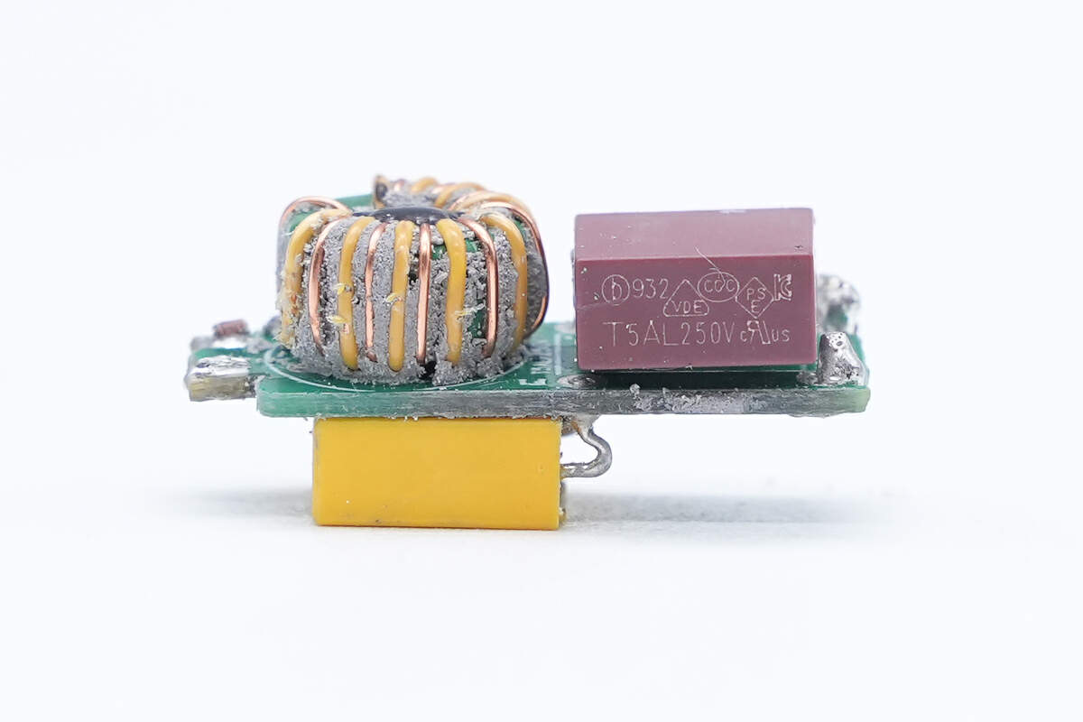
The common mode choke is wound with double wires to filter out EMI interference.
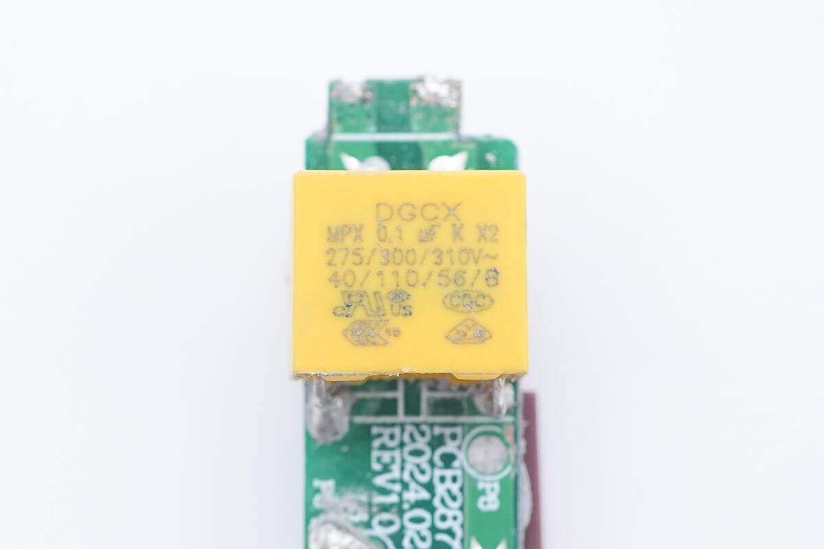
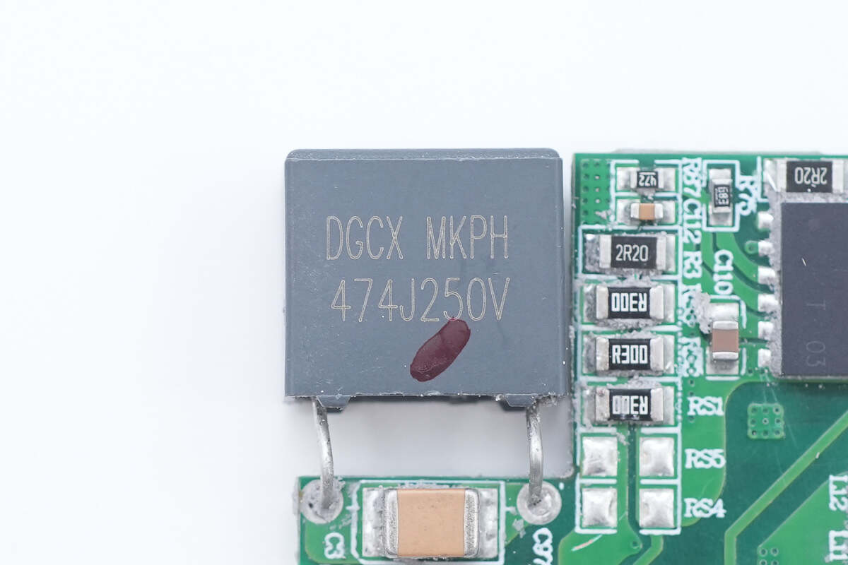
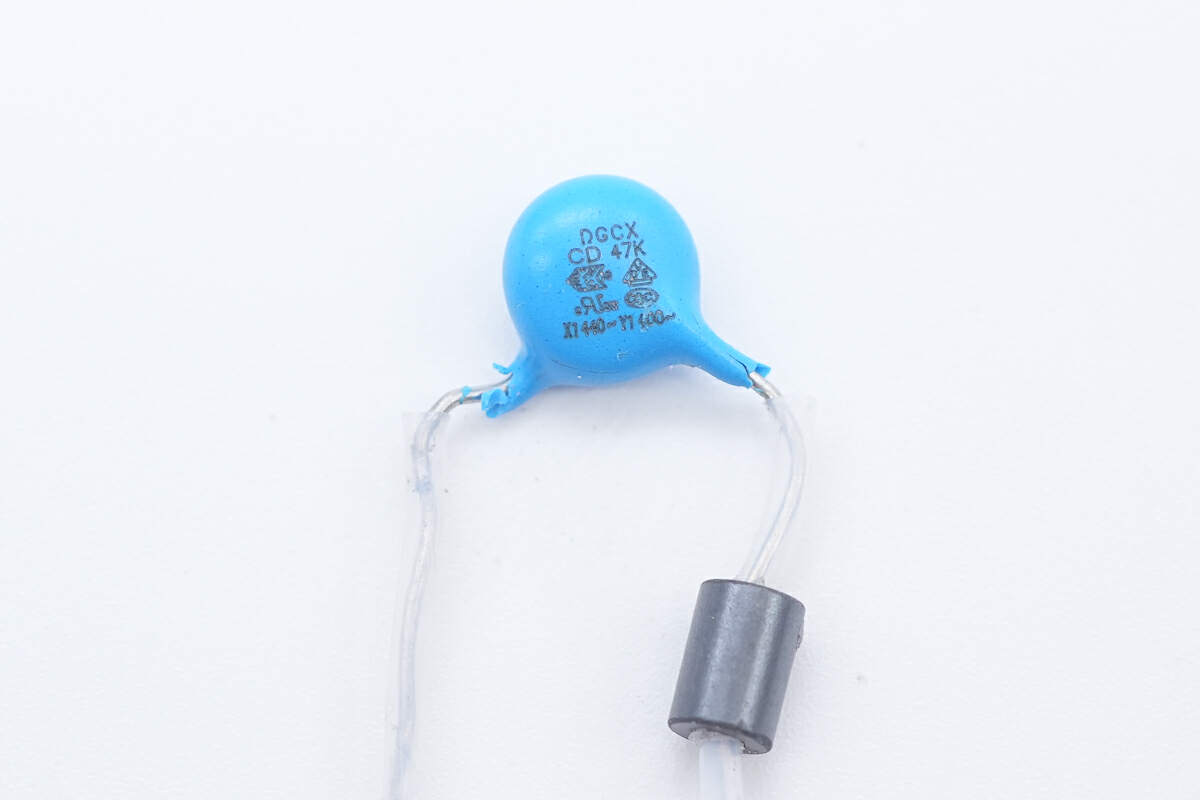
The safety X2 capacitor on the back is from DGCX. 0.1μF.
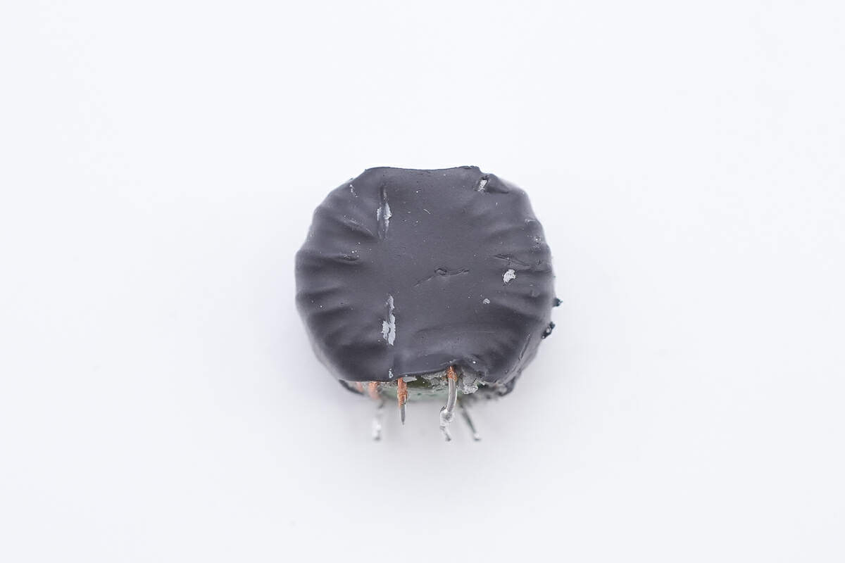
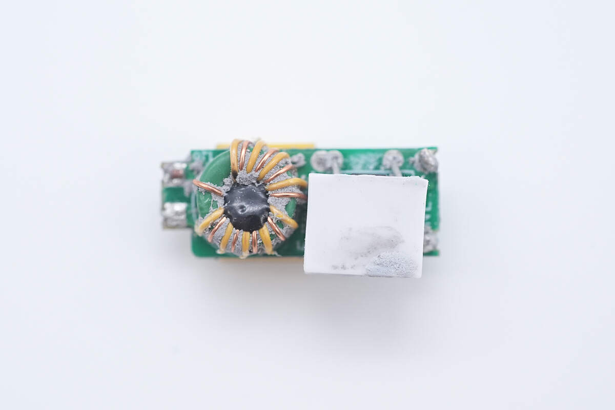
The secondary common mode choke on the PCBA is insulated by heat-shrinkable tubing.
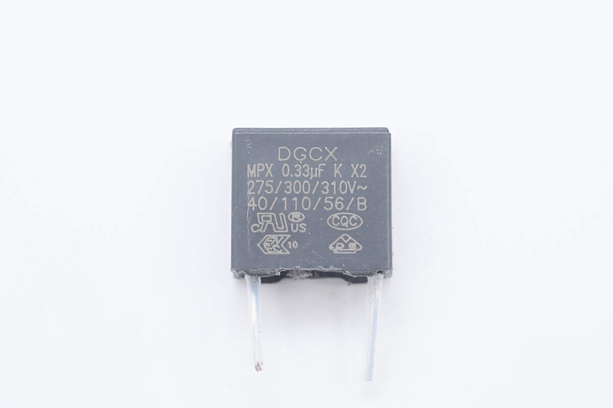
The other grey safety X2 capacitor is also from DGCX. 0.33μF.
The two bridge rectifiers are attached together and covered with a U-shaped heat sink, which is then wrapped with insulating tape.
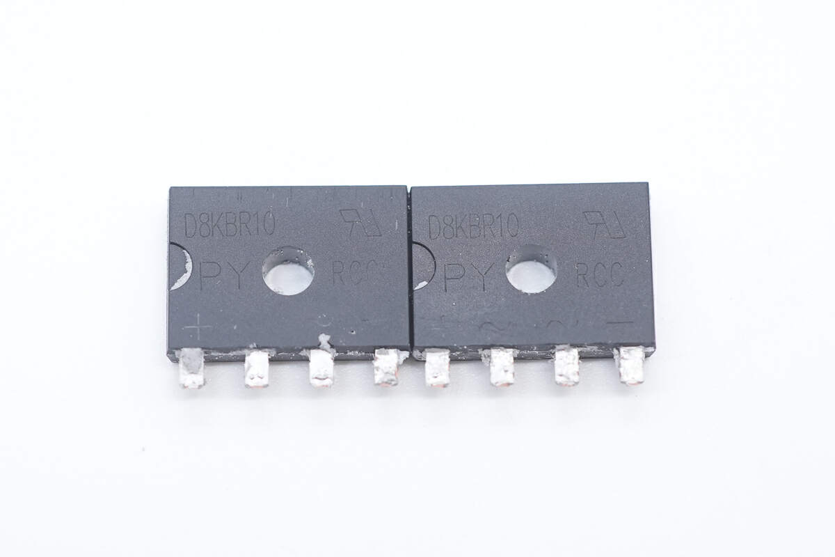
The two bridge rectifiers are from PY and adopt D3K package. Model is D8KBR10A. 8A 1000V.
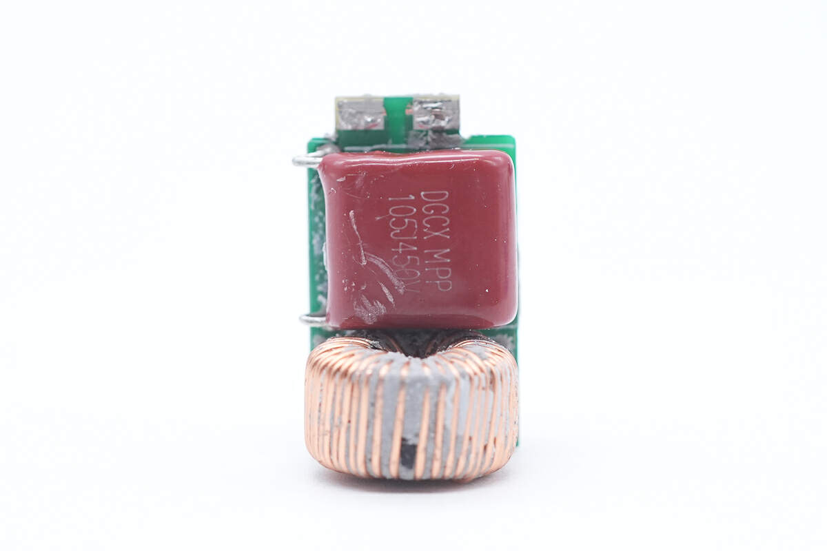
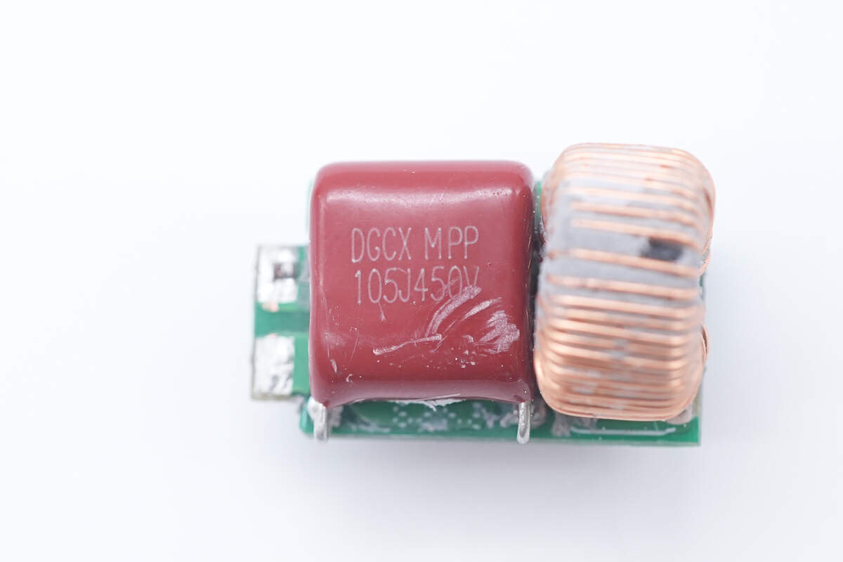
There is also a PFC boost inductor on one side of the PCBA module and a film filter capacitor on the small PCB on the side.
Remove the small PCB. There is a film filter capacitor and a filter inductor on the other side.
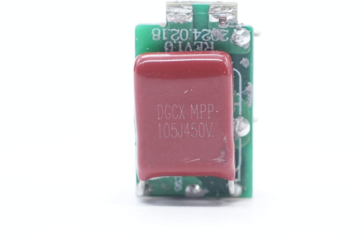
The MPP film filter capacitor is also from DGCX. 1μF 450V.
The other thin film filter capacitor is of the same model.
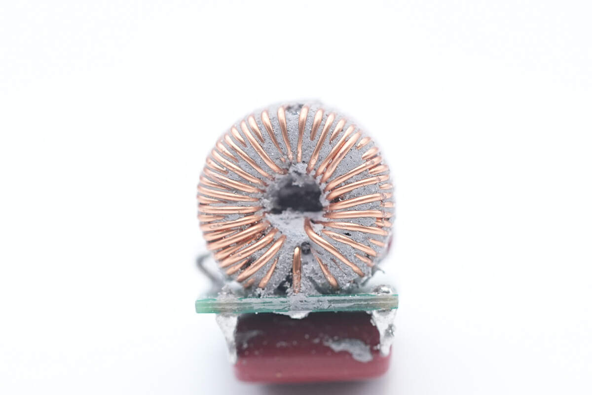
This is the filter inductor.
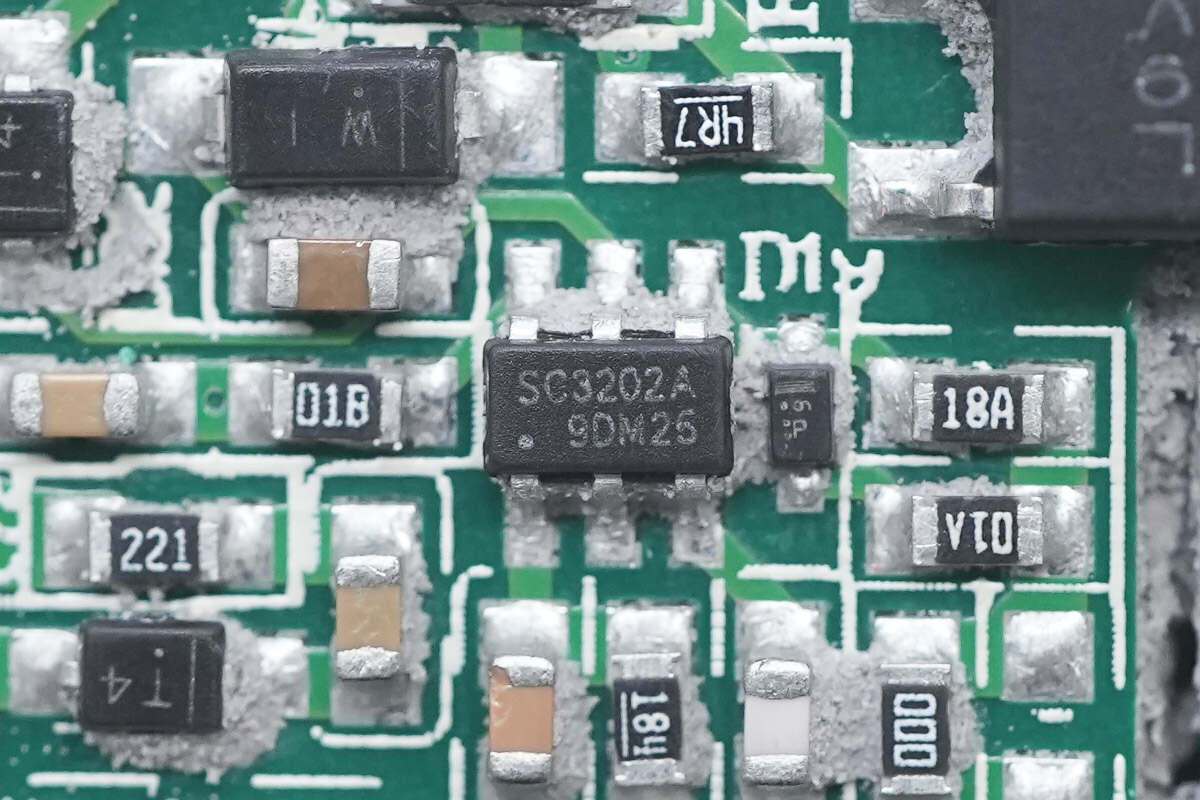
The PFC controller is from SouthChip. Model is SC3202.
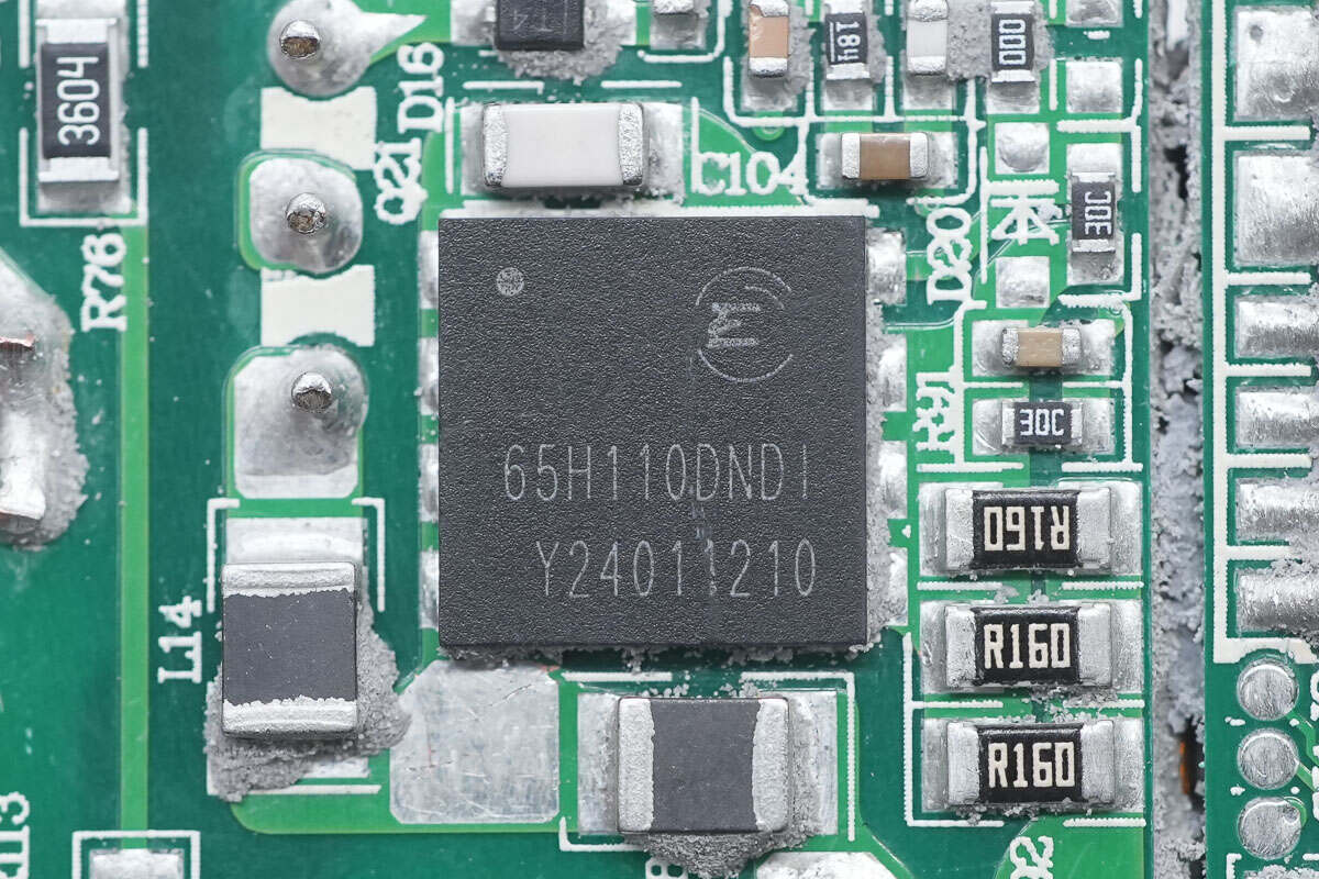
The PFC MOSFET is from CorEnergy and adopts DFN8*8 package. This cascode CoreGaN device uses CorEnergy depletion process technology, with a withstand voltage of 650V, a transient withstand voltage of 800V, and an on-resistance of 110mΩ. It has an extremely low gate charge, which makes the device switch fast and has low loss, which can greatly improve the system's energy efficiency. Its gate drive voltage range is ±20V, which greatly improves system reliability, is compatible with traditional silicon MOS drivers and simplifies circuit design. Model is CE65H110DNDI.
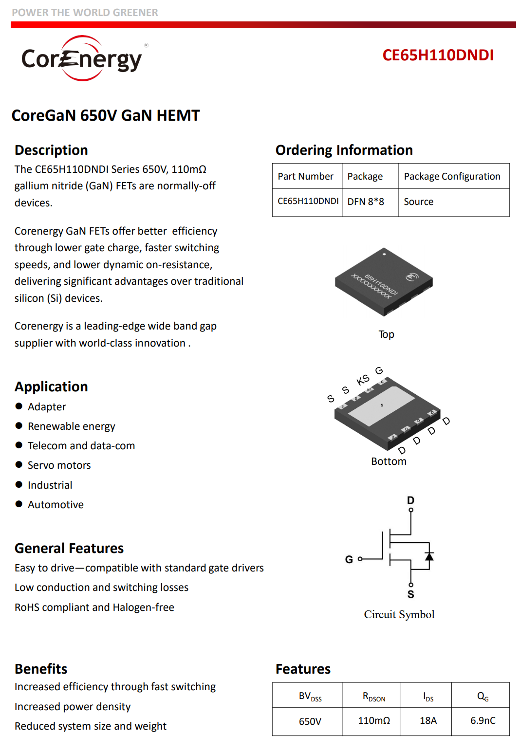
Here is the information about CorEnergy CE65H110DNDI.
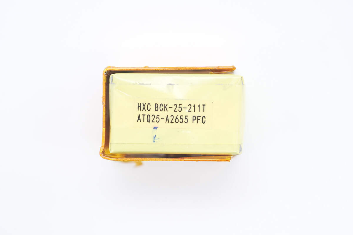
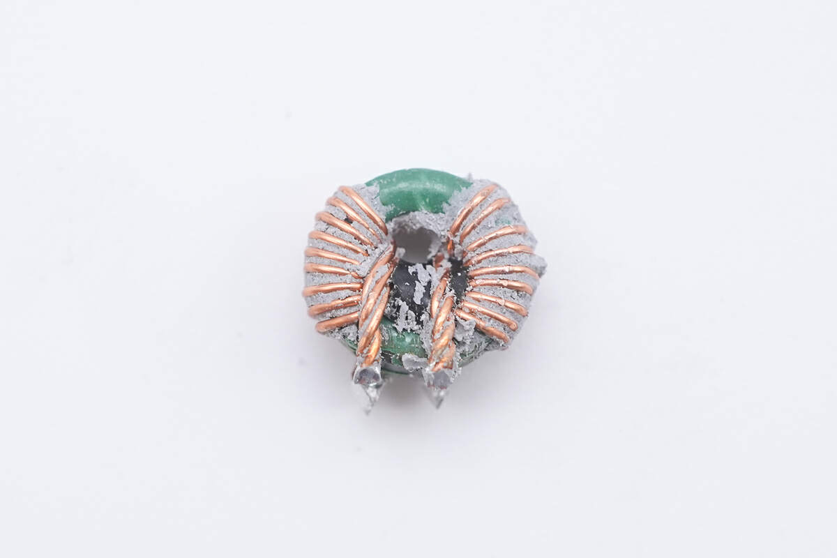
The PFC boost inductor uses ATQ25 magnetic core and is wrapped with copper heat sinks on three sides, which greatly enhances the heat dissipation performance and EMI shielding effect.
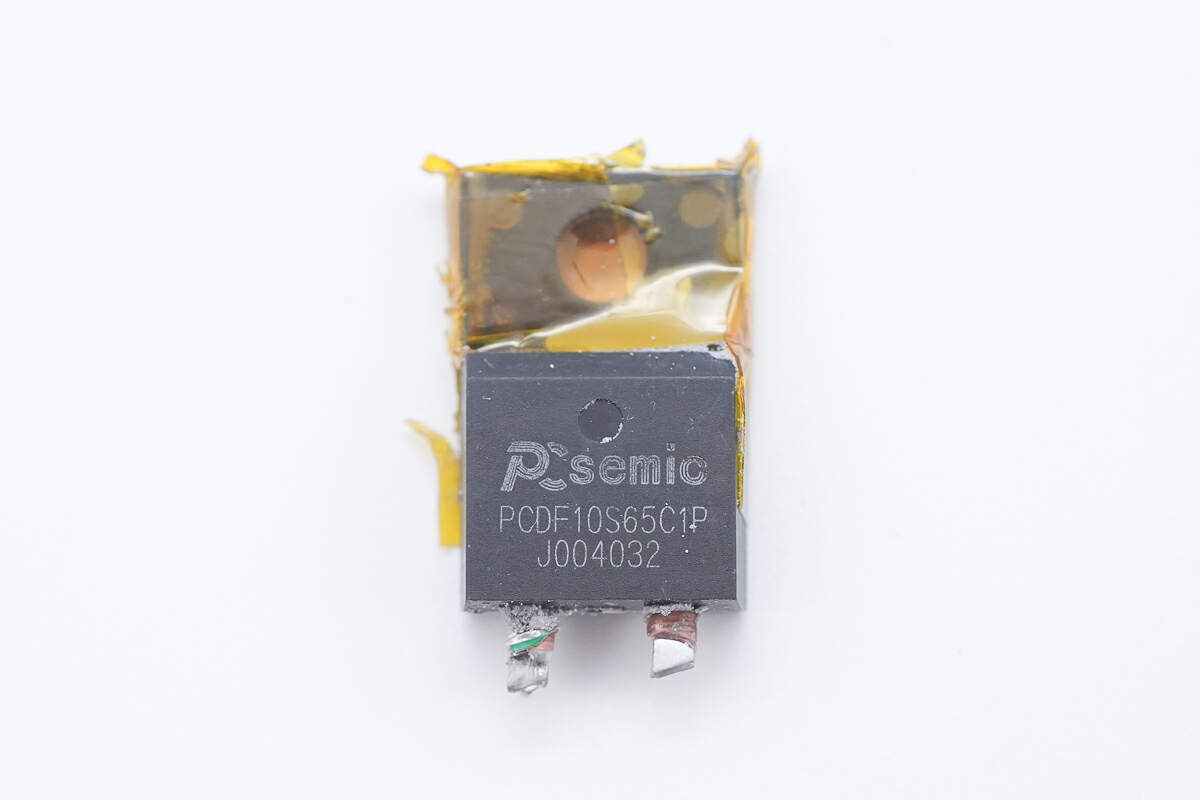
The PFC synchronous rectifier is from PCsemic. Model is PCDF10S65C1P.
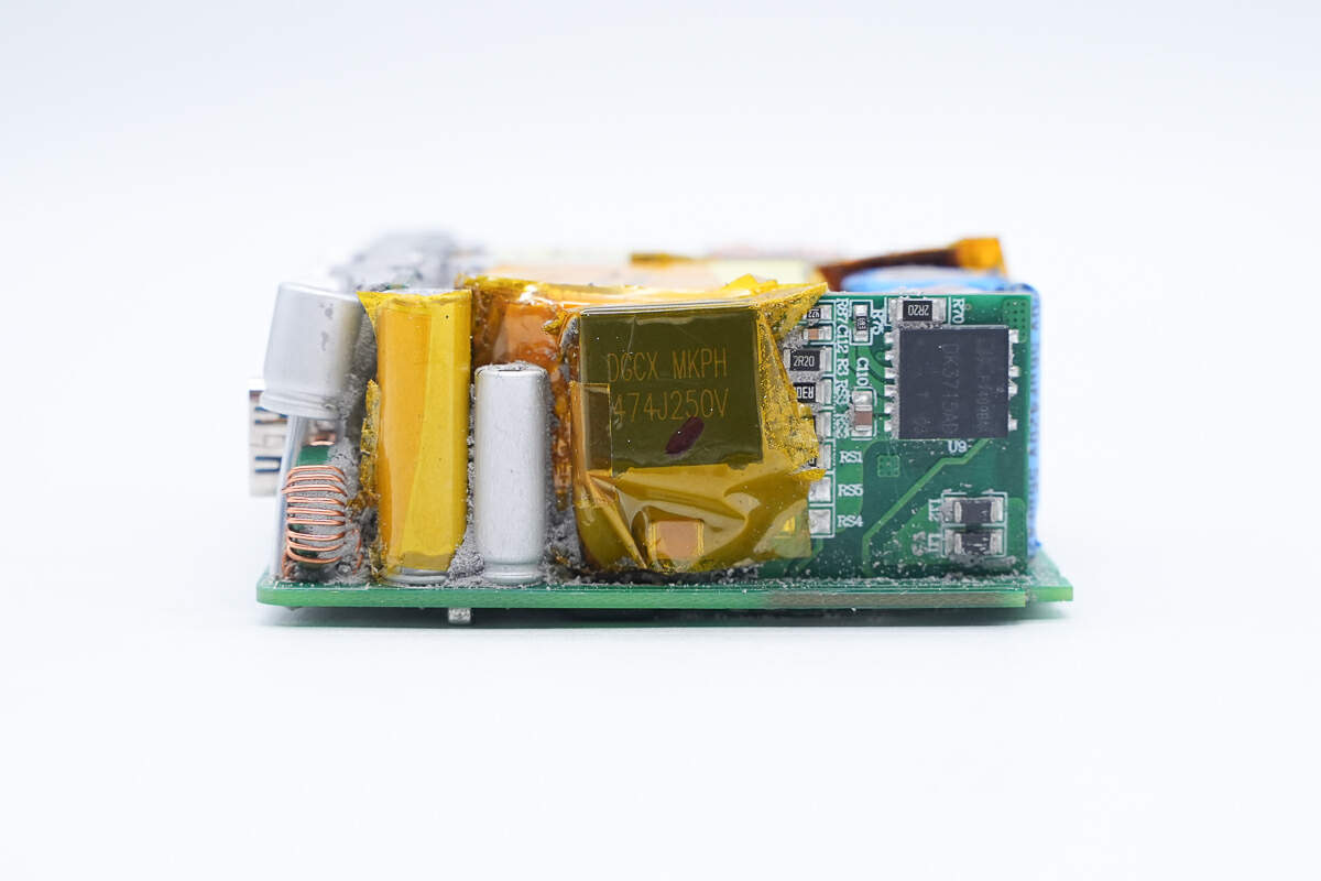
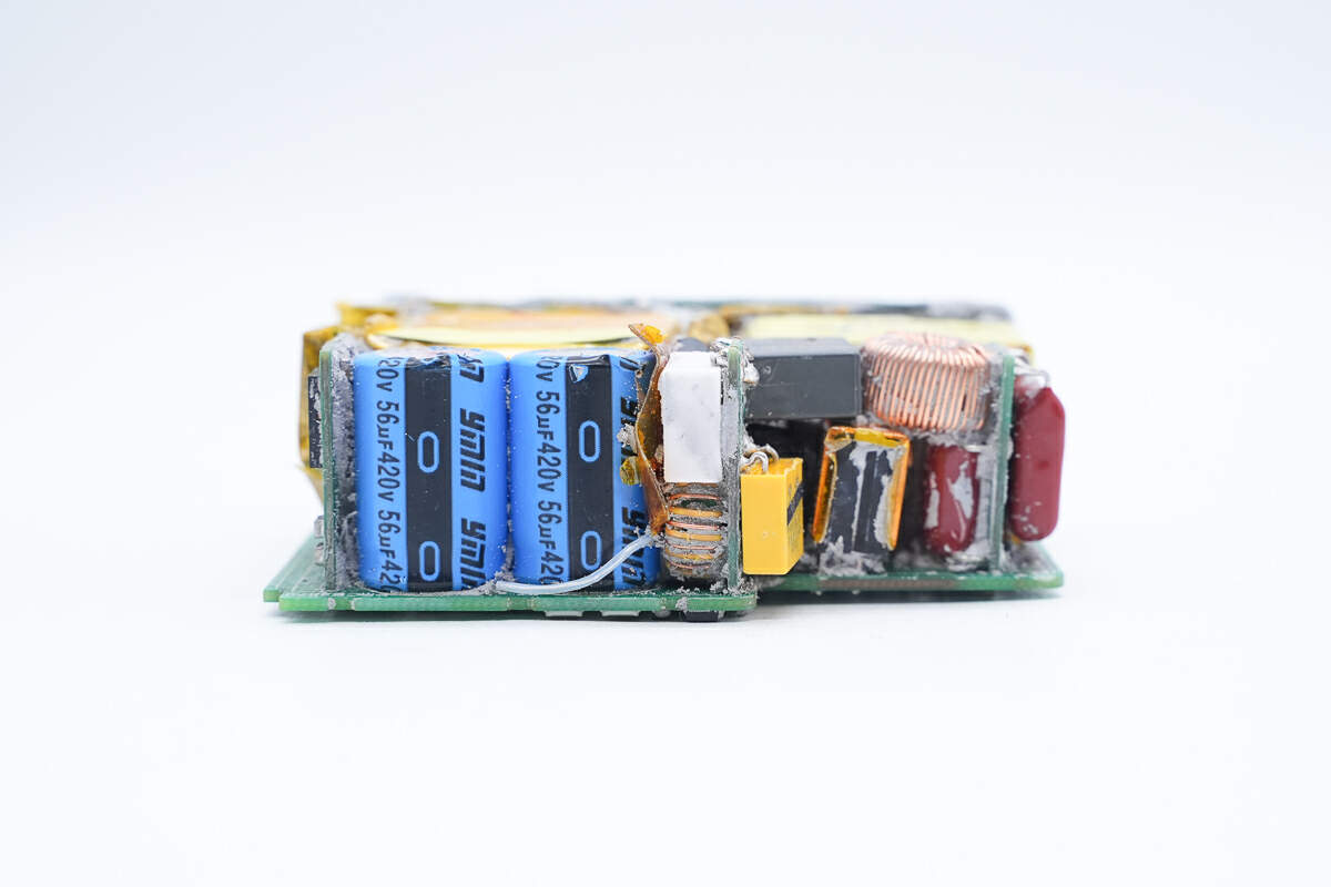
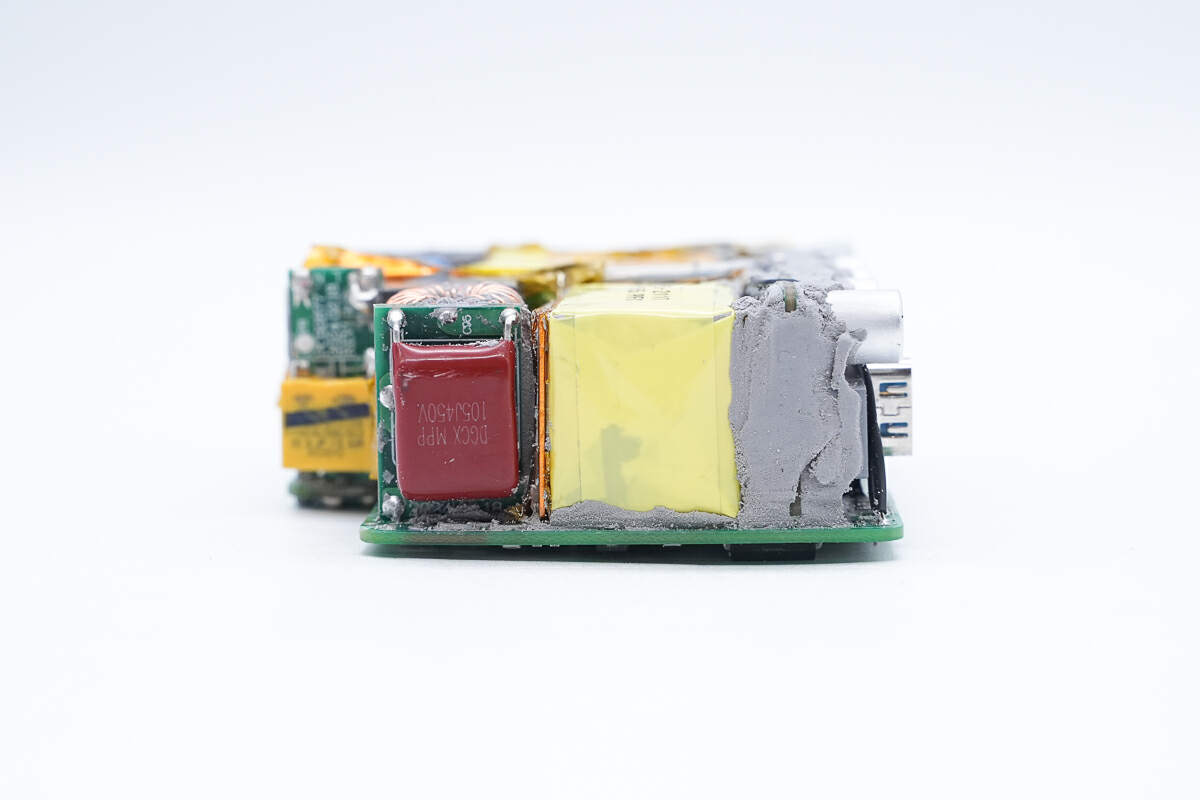
On the other side of the PCBA module, there are resonant capacitors and a master control chip on the small PCB. The resonant capacitor is wrapped with insulating tape, and on the left side, there are three solid capacitors for output filtering and a filter inductor, of which the larger solid capacitor is also wrapped with insulating tape.
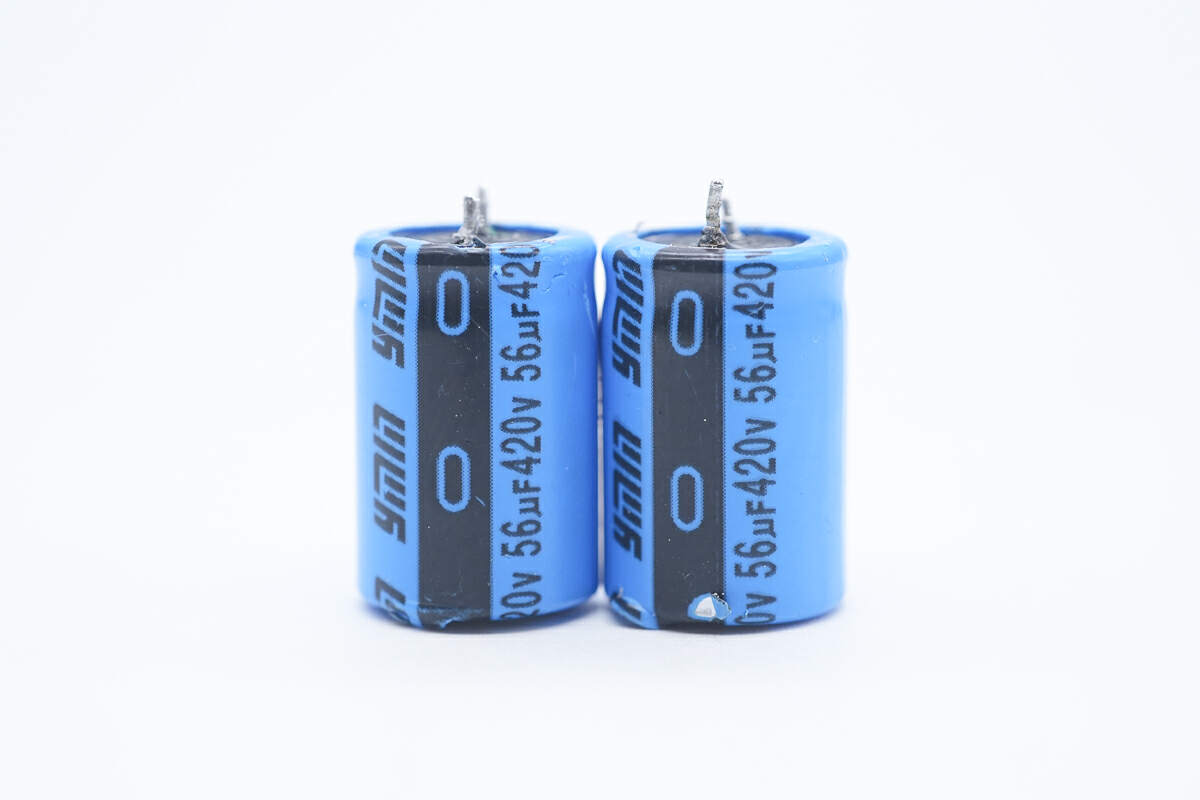
The two blue high-voltage filter electrolytic capacitors are from YMIN. 420V 56μF.
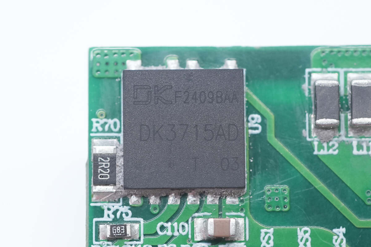
The switching power supply master chip is from DK. Model is DK3715AD.
The resonant capacitor is also from DGCX. 0.47μF 250V.
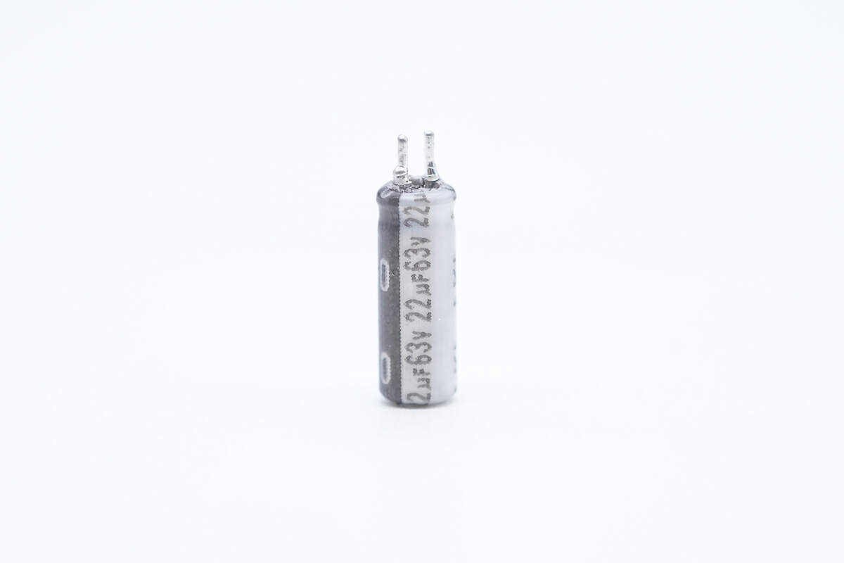
The capacitor that powers the master control chip is from YMIN. 63V 22μF.
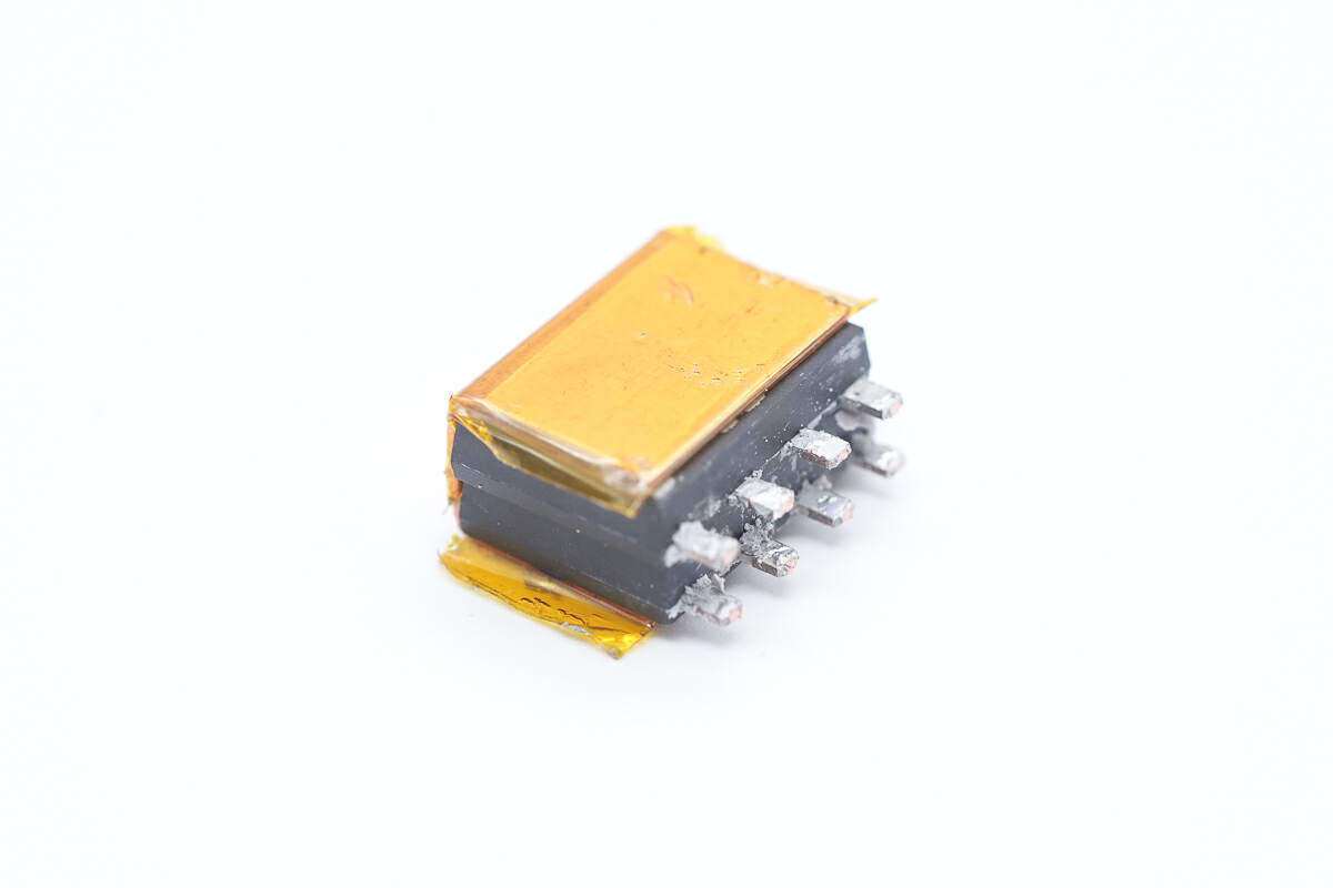
The transformer uses ATQ27 magnetic core.
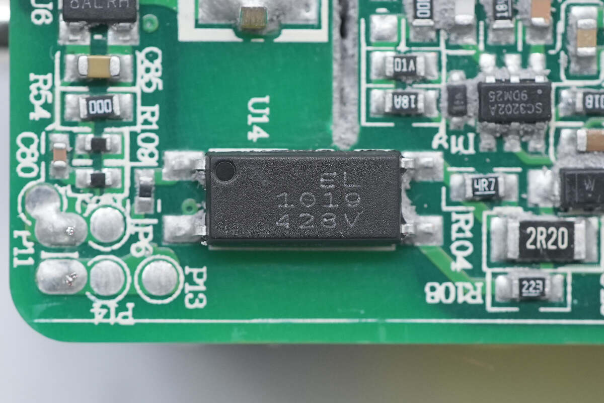
The Everlight EL 1019 optocoupler is used for output voltage feedback.
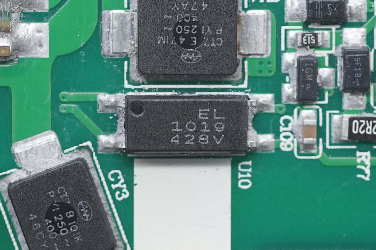
Another same optocoupler.
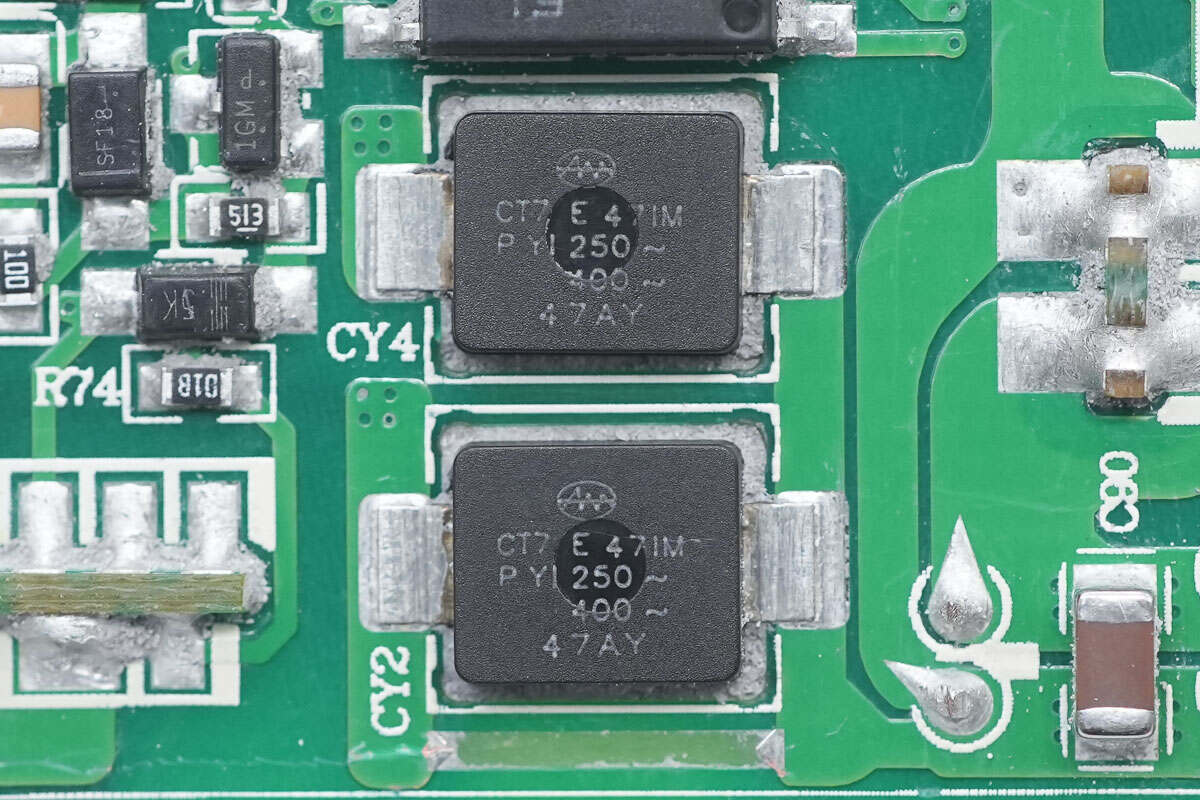
The two SMD Y capacitors are from KeiFat.
This is another SMD Y capacitor.
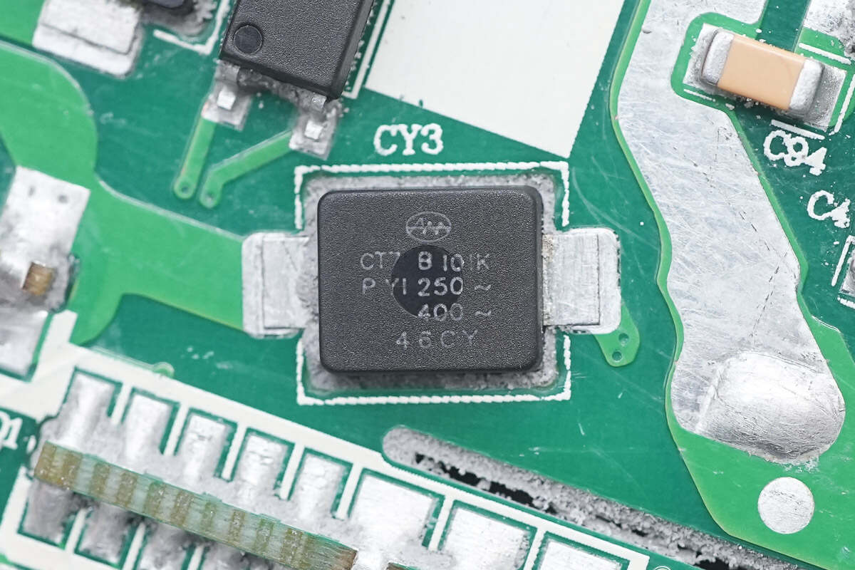
The blue Y capacitor is from DGCX.
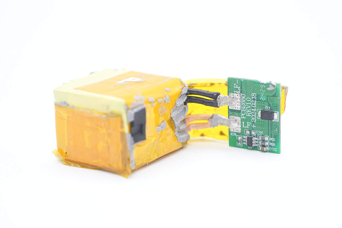
The transformer is connected to the synchronous rectifier small PCB and wrapped together with tape.
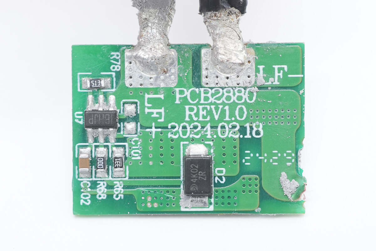
There is a synchronous rectifier controller on the front of the small PCB.
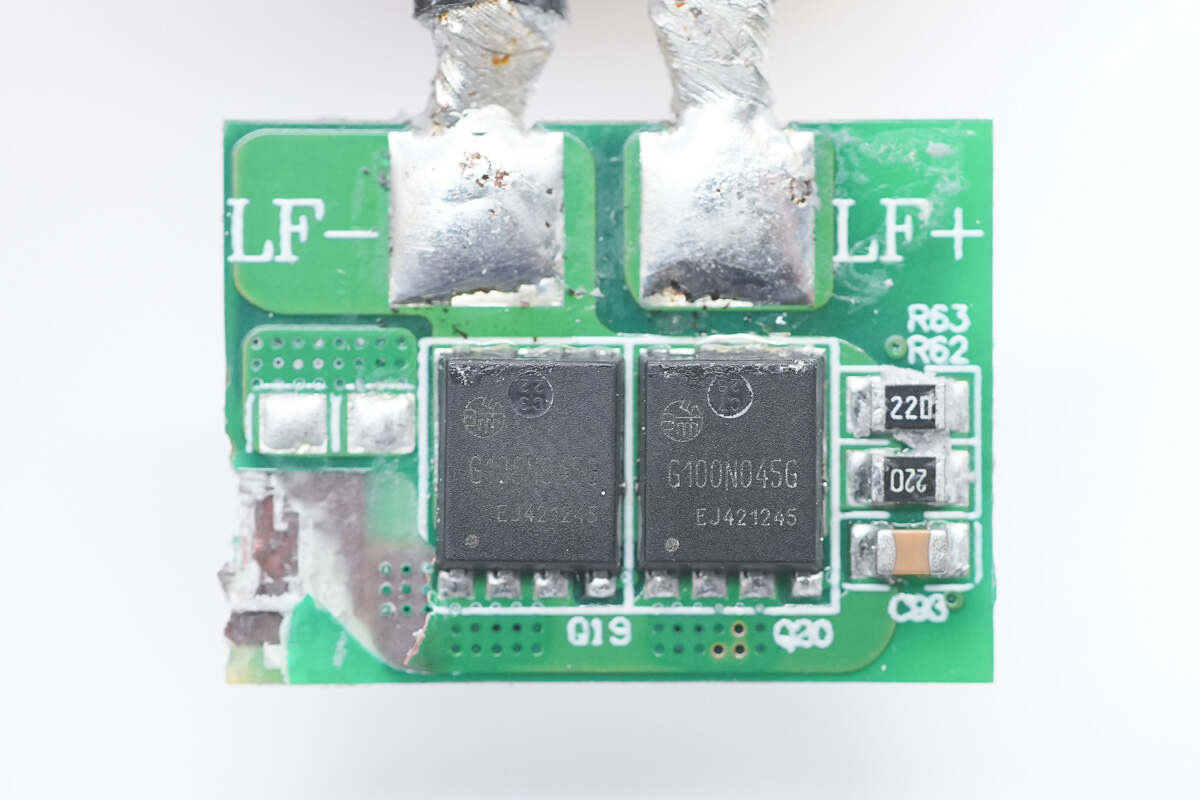
There are two synchronous rectifiers on the other side.
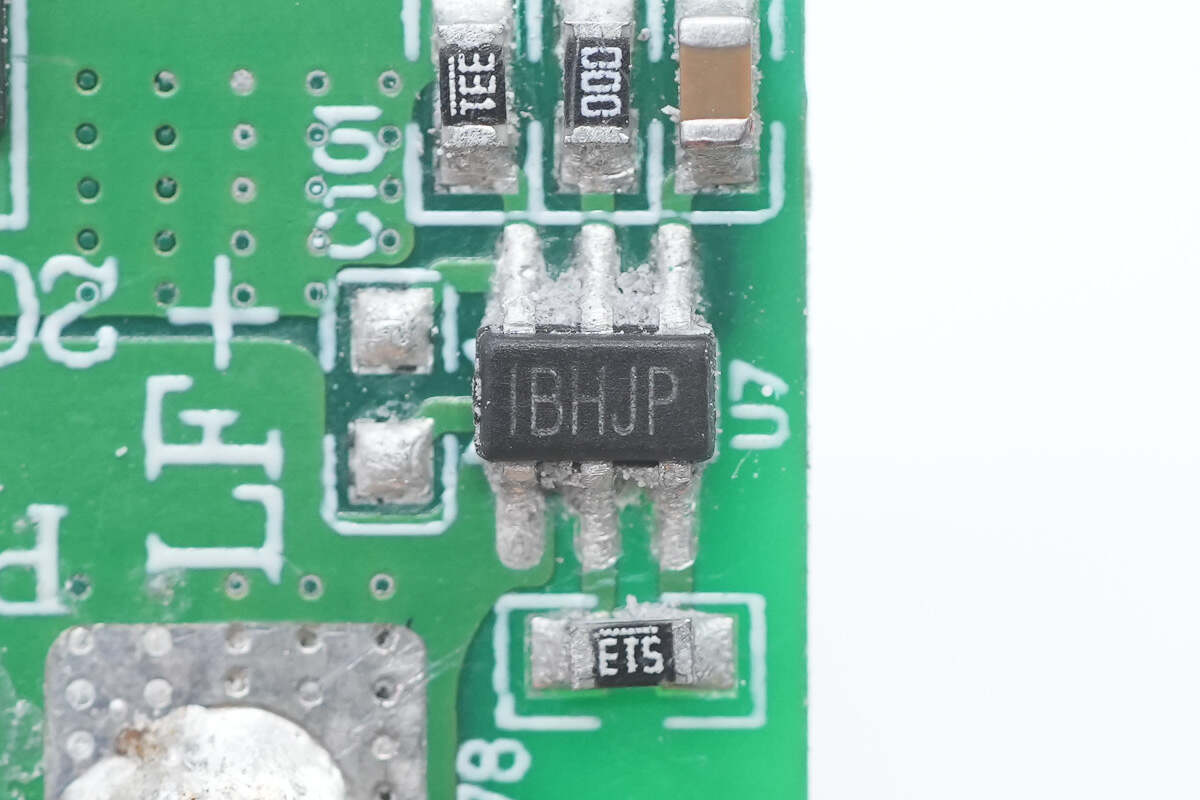
The synchronous rectifier controller marked with IBHJP is from MPS. Model is MP6908A.
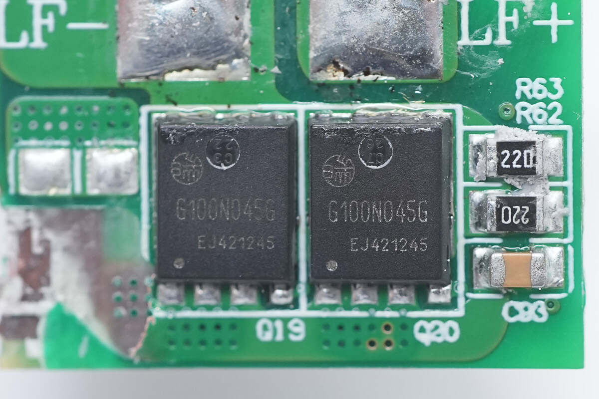
The two synchronous rectifiers marked with G100N045G are from HRmicro.
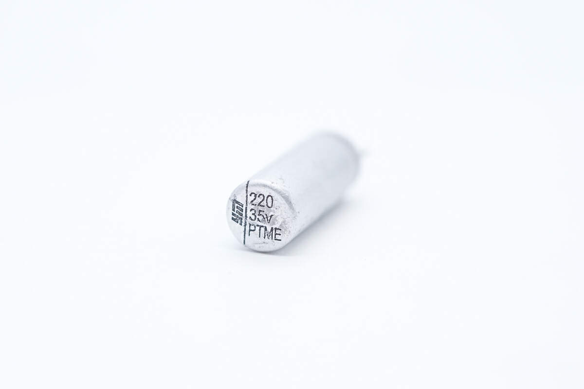
The solid capacitor for output filtering is also from YMIN. 35V 220μF.
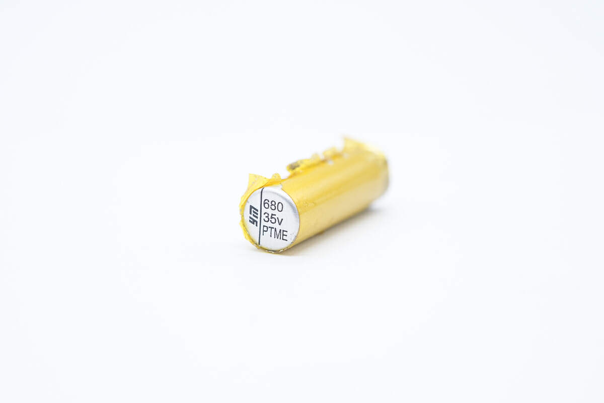
Another solid capacitor is wrapped with insulating tape. 35V 680μF.
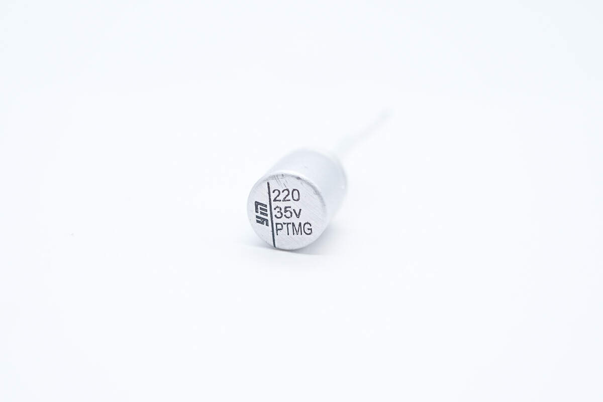
This is the third solid capacitor. 35V 220μF.
This is the filter inductor.
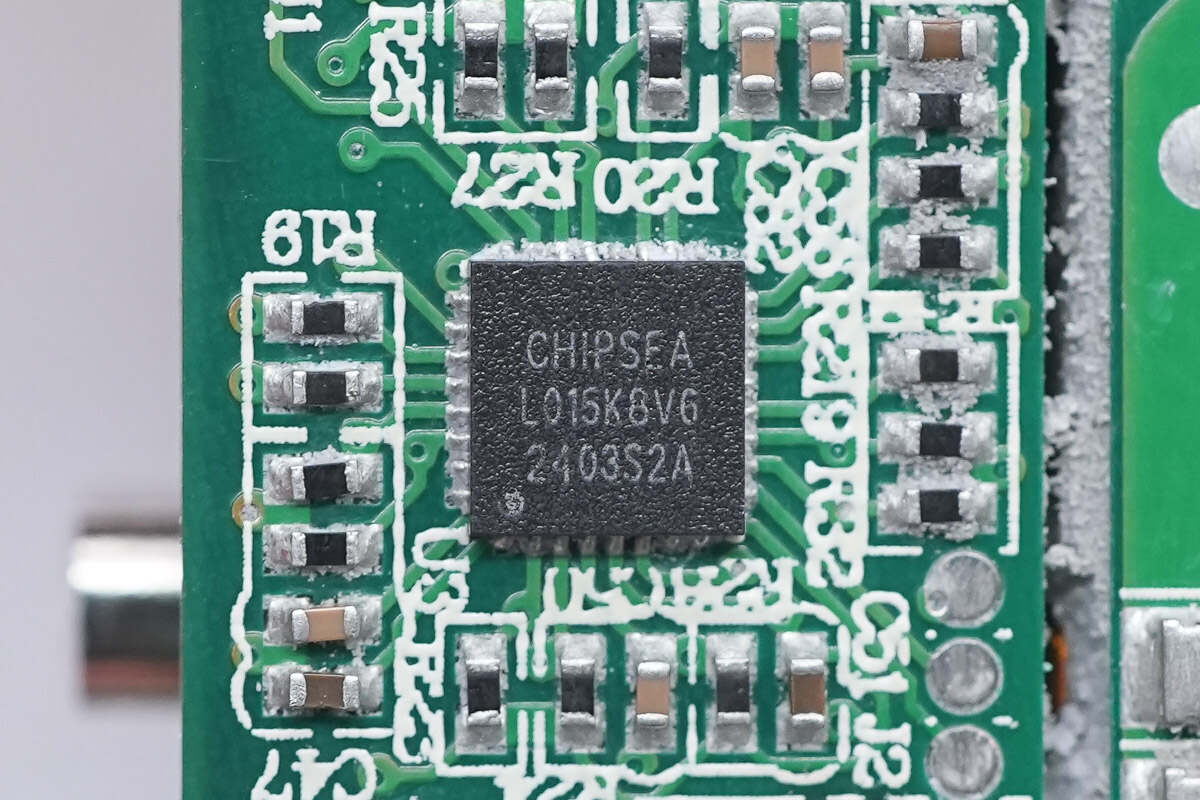
The MCU is from CHIPSEA. It is used for the intelligent distribution of multi-port output power. Model is CS32L015.
The output small PCB is also covered with potting compound, the sockets are protected, and there is a thermistor on the PCBA module.
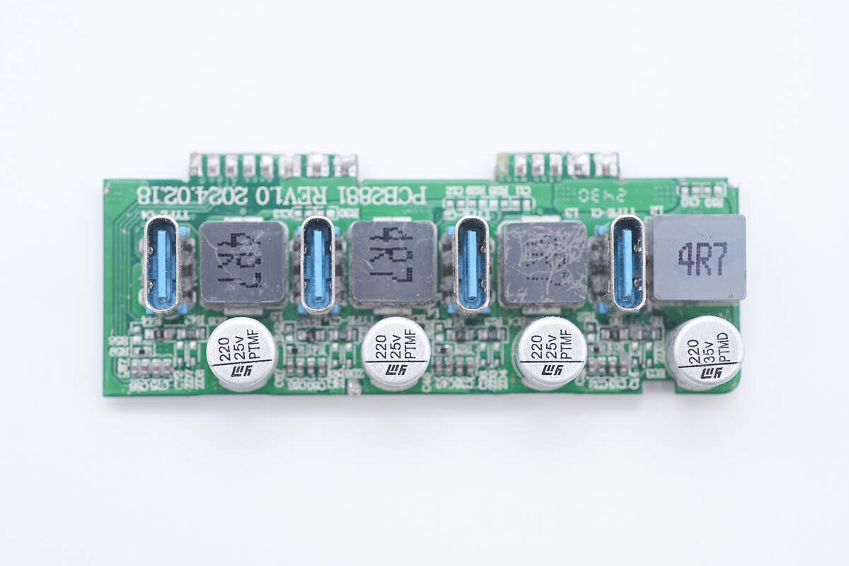
Remove the small PCB and clean the potting compound. On the front, there are buck inductors of the four secondary buck circuits and secondary filter solid capacitors.
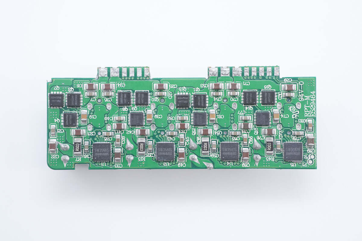
On the back, there are buck protocol chips with four secondary buck circuits, synchronous buck MOSFEs, and output VBUS MOSFETs. The four circuits are independent of each other.
The thermistor is used to monitor the internal temperature of the charger.
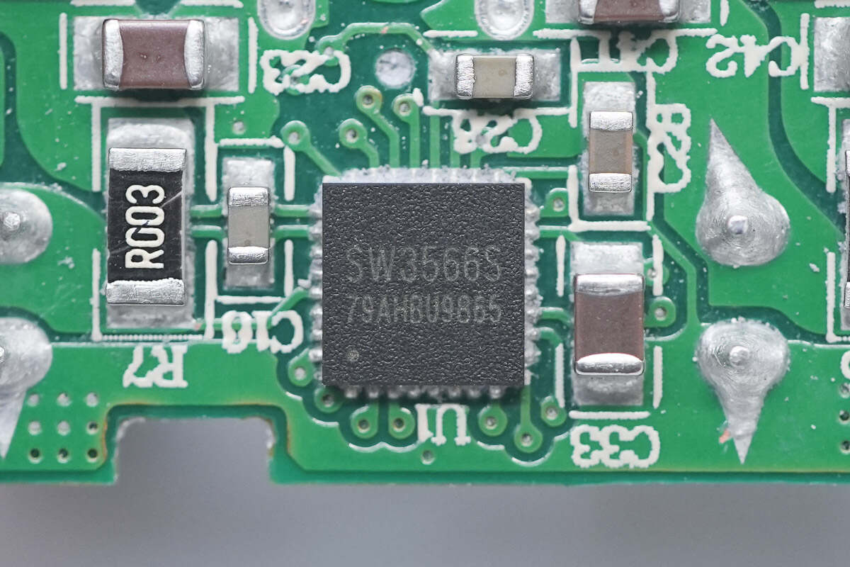
The secondary step-down circuit control chip of the USB-C1 port is from iSmartWare. Model is SW3566S.
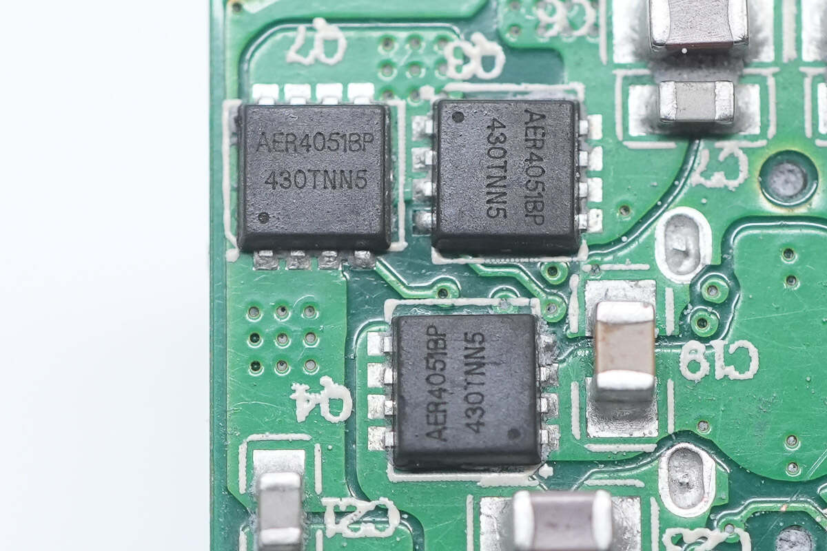
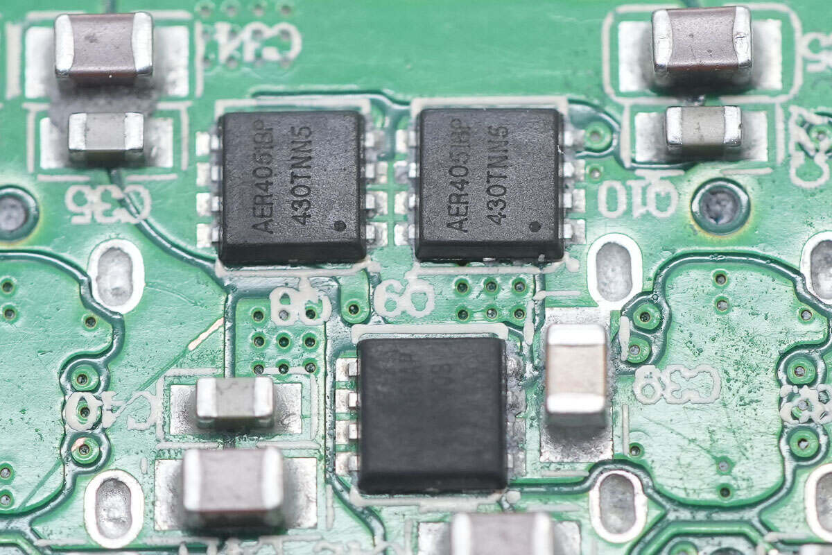
The two synchronous buck MOSFETs and the output VBUS MOSFET are from ALLEPIC. Model is AER4051BP.
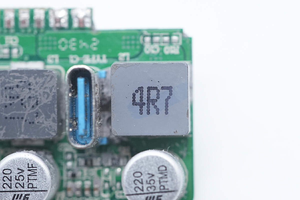
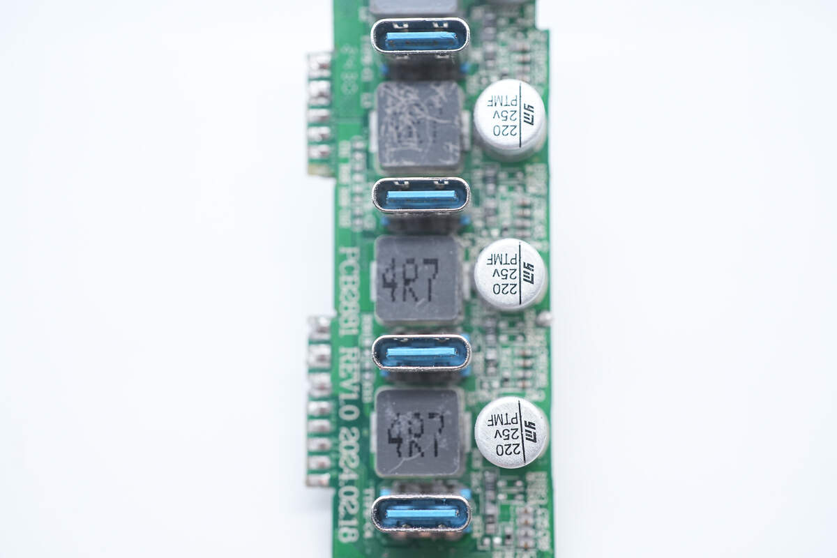
This is the step-down inductor. 4.7μH.
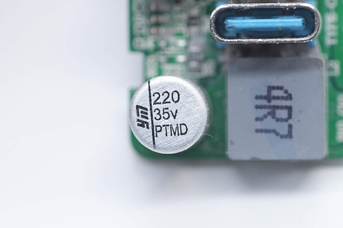
The secondary step-down solid capacitor for output filtering at the USB-C1 port is also from YMIN. 35V 220μF.
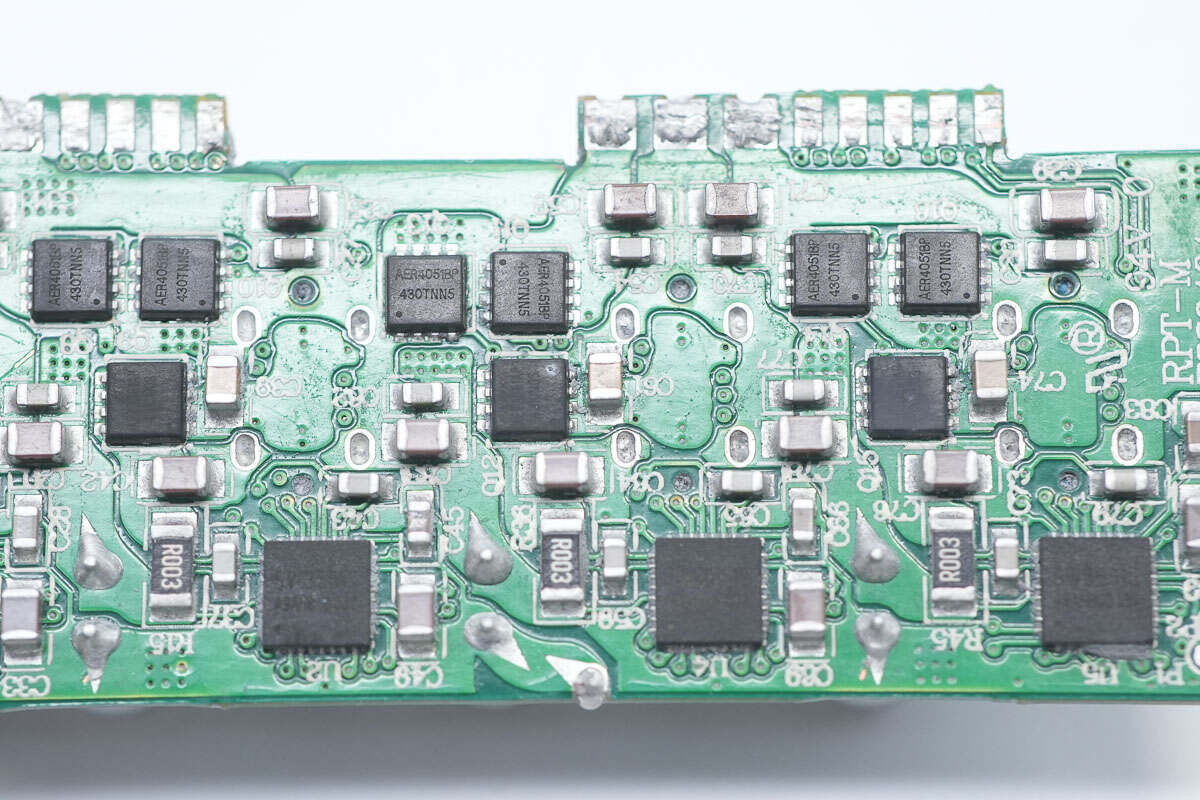
The other three USB-C ports have the same secondary step-down circuit schemes, and one of them is used as an example for demonstration.
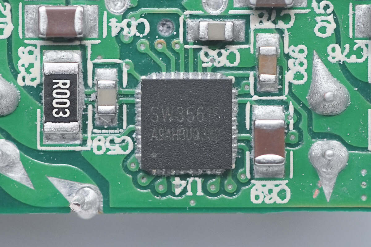
The step-down protocol chips of the USB-C2/3/4 port are all from iSmartWare. Model is SW3561S.
The two synchronous buck MOSFETs and the output VBUS MOSFET of the three power components are also from ALLEPIC. Model is AER4051BP.
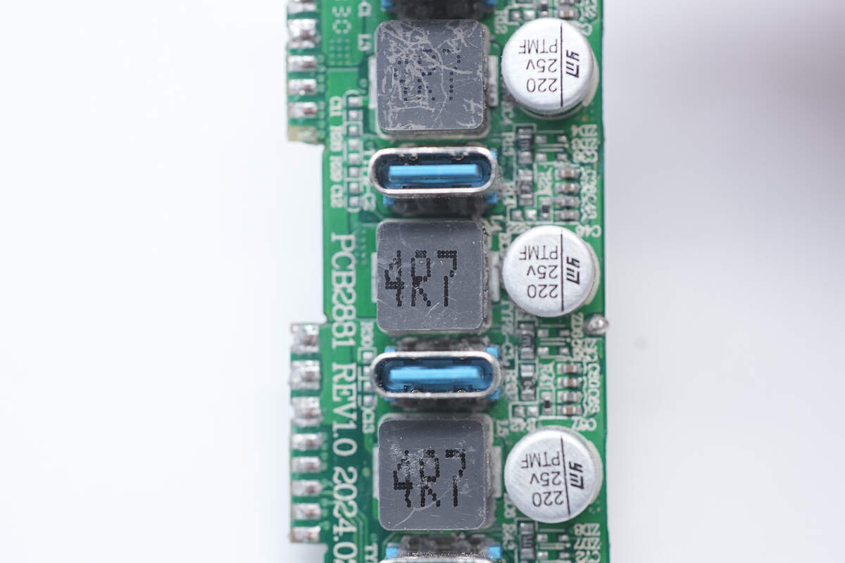
These are the buck inductors of the three buck circuits.
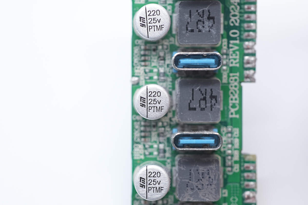
The three secondary filter solid capacitors are also from YMIN. 25V 220μF.
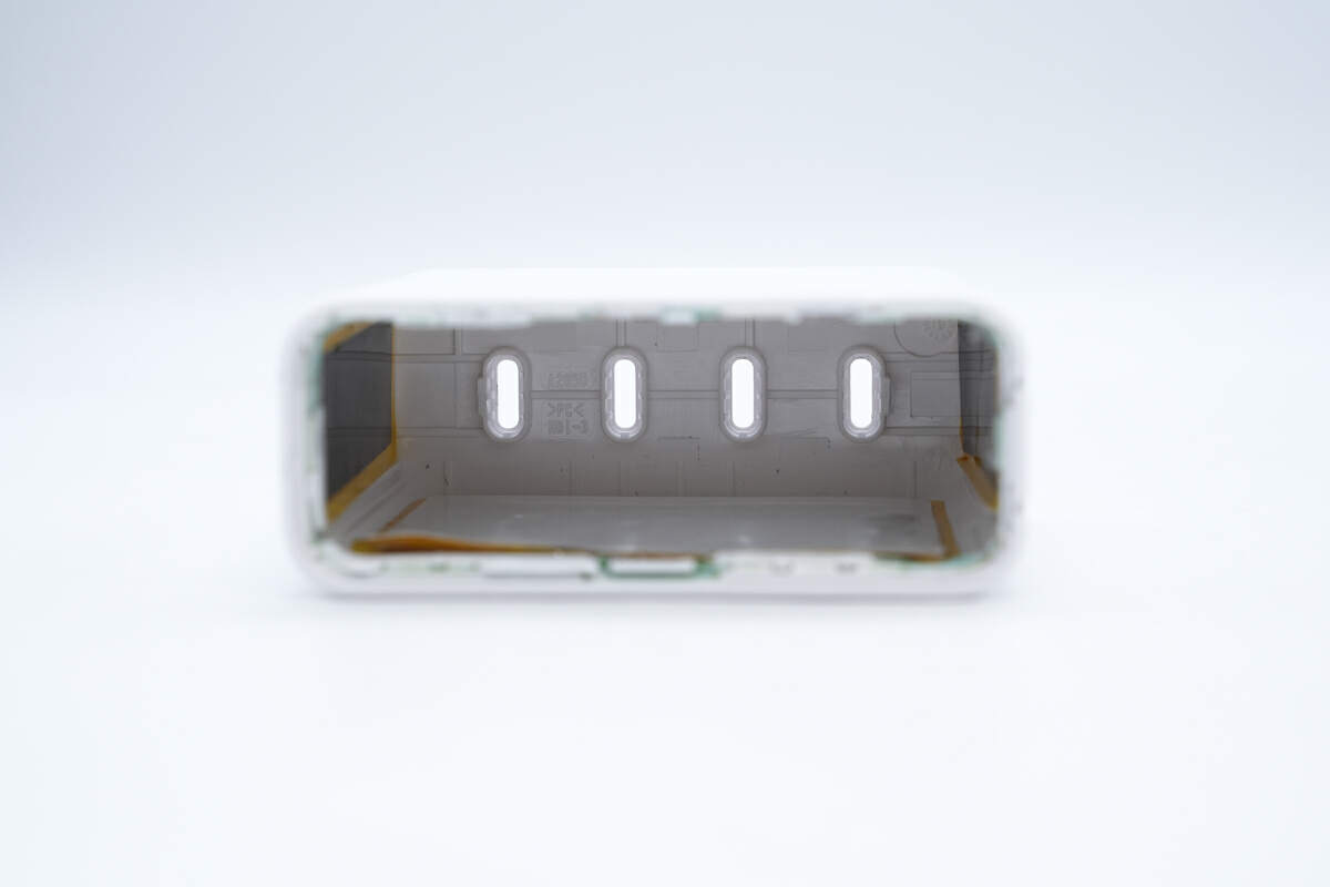
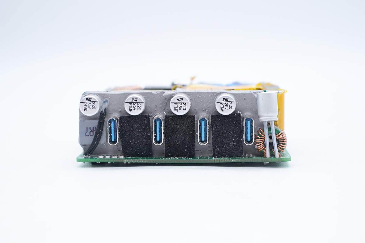
These are four USB-C sockets.
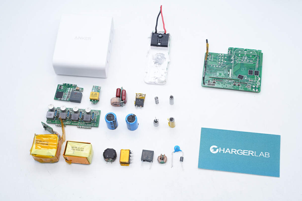
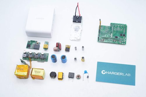
Well, those are all components of the ANKER 150W 4 Ports GaN Charger.
Summary of ChargerLAB
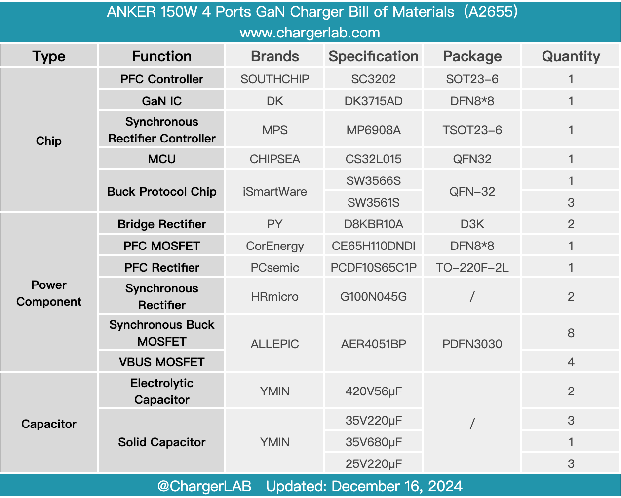
Here is the component list of the ANKER 150W 4 Ports GaN Charger for your convenience.
Its design style is simple, and the shell is made of PC flame-retardant material, which is safe and reliable. The surface is matte and feels very good to the touch. Compared with competing products on the market, its biggest feature is that each interface can support high-power fast charging of more than 100W, and the performance is quite impressive.
As an Apple-exclusive version, the only compatible protocol is PD fast charging. However, compared with Apple's original 140W GaN fast charging, it has advantages in size, number of ports, and performance. It is very suitable for Apple multi-device users to purchase and is suitable for daily home office and travel use.
After taking it apart, we found it uses PFC+AHB power architecture design. In addition, the PCBA module is filled with potting compound to improve heat dissipation, and heat sinks are added to the bridge rectifier, PFC boost inductor, and even the shell to help dissipate heat. Whether it is the overall or the details, the materials and workmanship of this product by Anker are quite good.
Related Articles:
1. Teardown of Anker Prime Charger (200W, 6 Ports, GaN)(A2683)
2. Teardown of Anker Prime 200W 6 Ports GaN Charger
3. Trump Same Style | Teardown of Anker MagGo Magnetic Power Bank (A1654)