You can buy it on Amazon: https://amzn.to/38V2j4Z
If you wanna buy the tester of POWER-Z, you can visit our Amazon store: Click here.
Introduction
---------------------------------------------------------------
ChargerLAB has published several teardown videos of Anker chargers in the past.
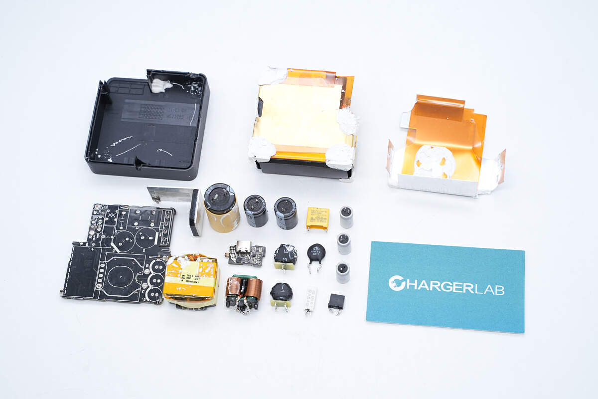
And today, we got another brand new Anker 100W GaN charger, which is equipped with two USB-C ports and a USB-A port.
Let’s try to take it apart and check what’s inside.
Bill of materials (BOM)
------------------------------------------
Time-delay Fuse: Better Electronics (3.15A 250V)
Safety X2 Capacitor: DGCX (0.47μF)
Bridge Rectifier: Pingwei D8KBR10
Film Capacitor: DGCX (0.47μF)
PFC Controller: ON Semiconductor NCP1622BEC
GaN IC: Navitas NV6136A
Electrolytic Capacitor: AiSHi (420V120μF)
Primary Controller: Southchip SC3022D
Optocoupler: EL1018
SMD Y Capacitor: Anshan KeiFat
Synchronous Rectifier: Vergiga VSP007N12MS-G
Solid Capacitor: Yongming (680μF 25V, 470μF 25V)
Buck Controller & Protocol Chip: Ismartware SW3516H
MOSFET (USB-C): AOS AONR21357 (30V, 6.3mΩ)
Output VBUS MOSFET: AOS AON7544 (30V, 5mΩ)
MCU: Chipsea CSU38F20

