Introduction
Infineon is the developer of the USB PD3.1 protocol, which can provide fast-charging charger components that meet different powers.
ChargerLAB got an XDPS2201 reference design from Infineon. It does not have large heat sinks and cooling fans, compared with traditional eBike chargers. So, it's suitable for a fully sealed case. Next, let’s take a look at the design of this module and take it apart to see its components.
Product Appearance
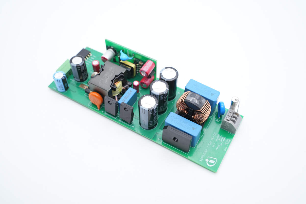
Infineon XDPS2201 has a simple design without a PFC circuit. It supports a wide input range of 198-264V~50/60Hz and an efficiency of more than 95% under 230V AC when fully loaded. Due to the high efficiency, there is no need for heat sinks, as long as a certain gap is left to meet the temperature requirements.
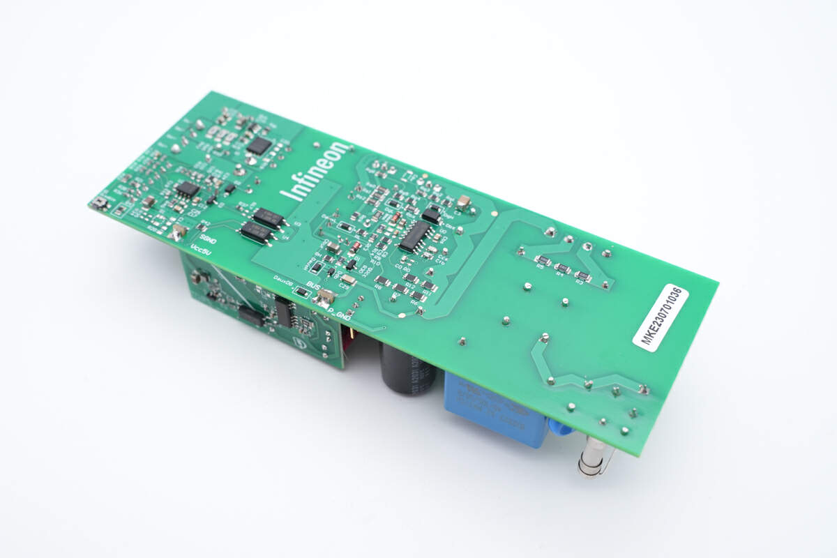
The master control chip, optocoupler, and other components are on the back. The circuit design is simple.
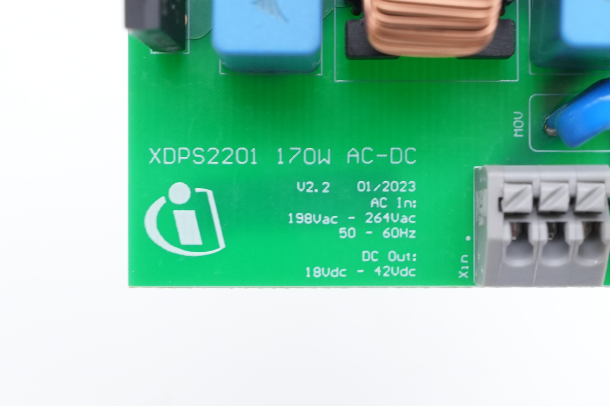
The AC input end has marked with the AC input voltage range of 198Vac-264Vac, frequency of 50-60Hz, and DC output of 18Vdc-42Vdc.
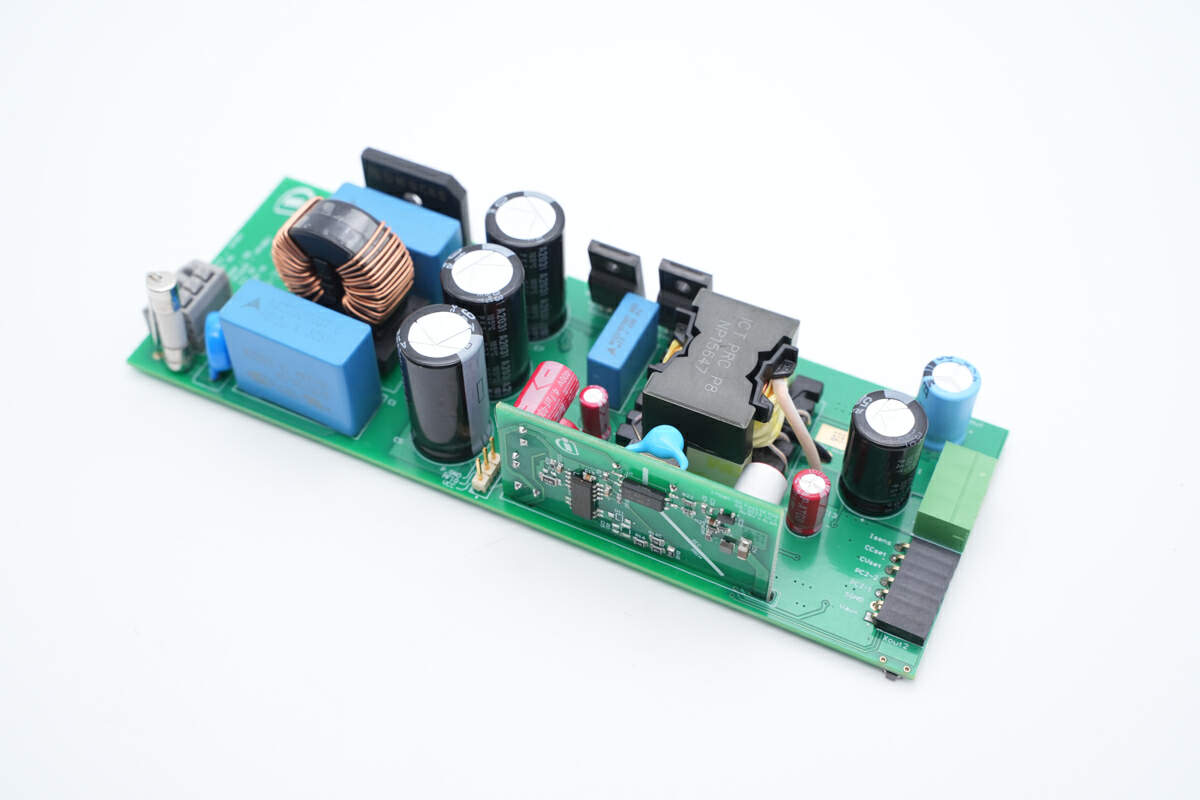
The PCB of the auxiliary power supply is soldered on one side of the PCBA module.
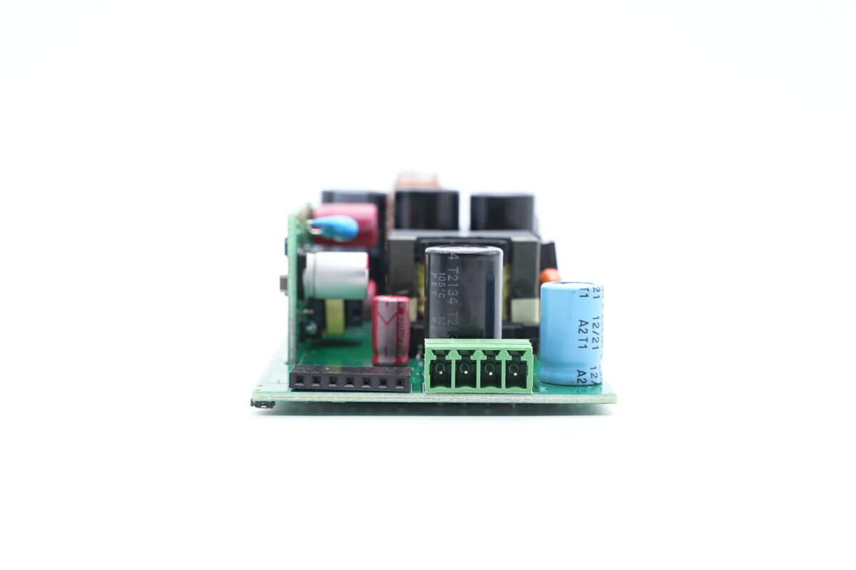
The output end of the PCBA has two connectors for easy assembly.
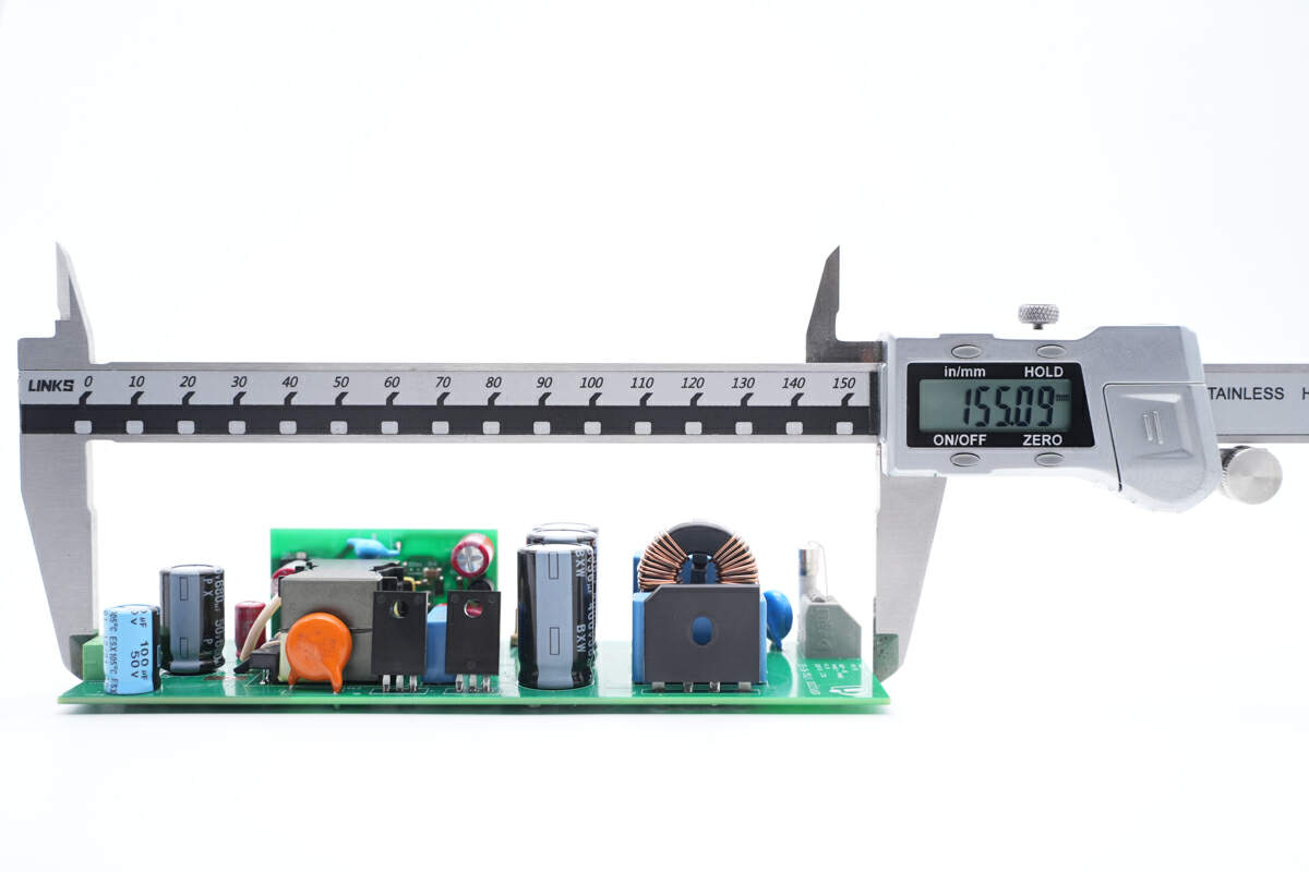
The length is about 155 mm (6.1 inches).
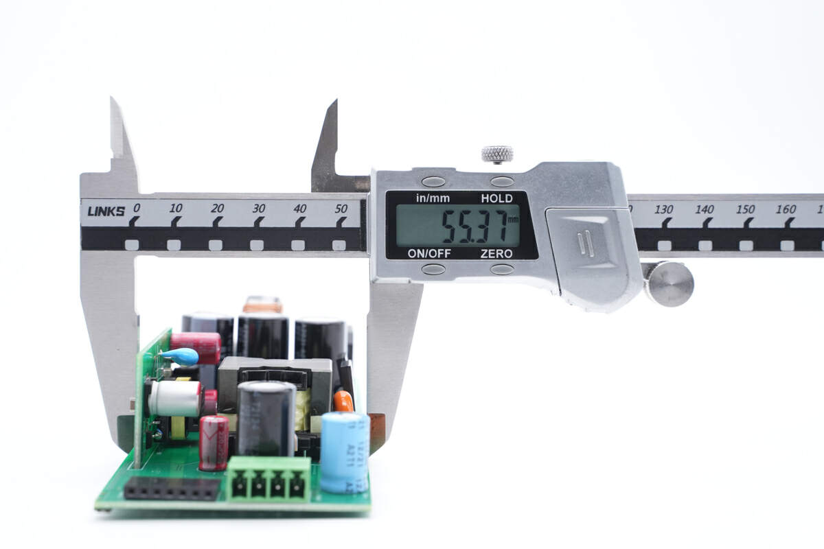
The width is about 55 mm (2.17 inches).
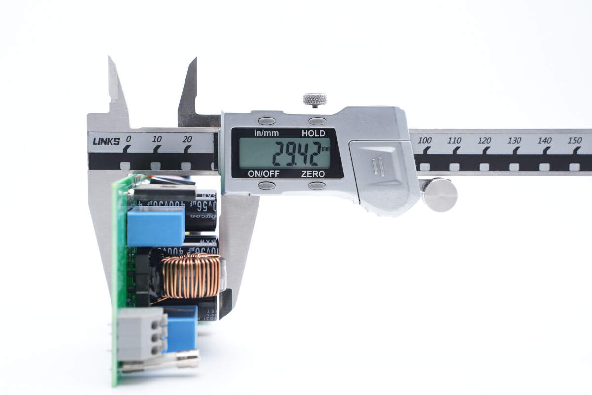
And the thickness is about 29 mm (1.14 inches).
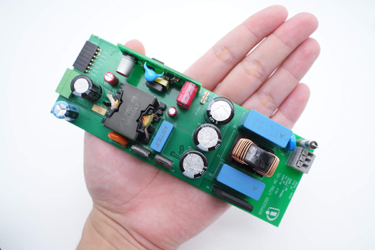
This is the size of the PCBA module in your hand.
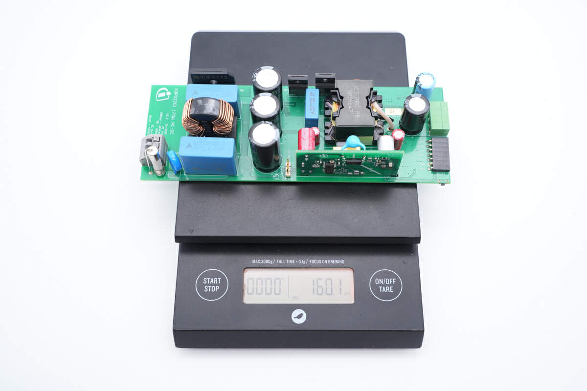
The weight is about 160 g (5.64 oz).
Teardown
Next, let’s dismantle this PCBA module and take a look at the design and components.
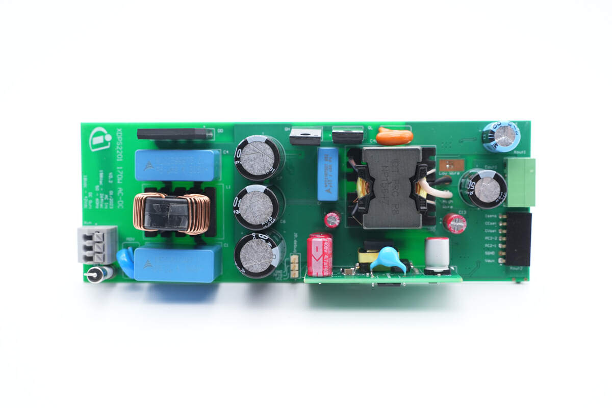
On the left of the PCBA module is the AC input end, there are connectors, fuse, and varistor. The safety X2 capacitor, common mode chock, and bridge rectifier are on the right of the AC input end. The PCB of the auxiliary power supply is at the bottom.
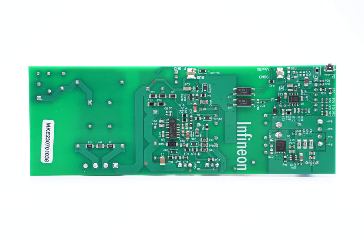
The hybrid-flyback controller, feedback optocoupler, synchronous rectification controller, and Op-Amp are on the back. The primary and secondary sides of the PCBA module are insulated. Most of the components are laid out sparsely and the power components are placed on the edge of the PCBA module, making it easy to install external heat sinks to improve heat dissipation.
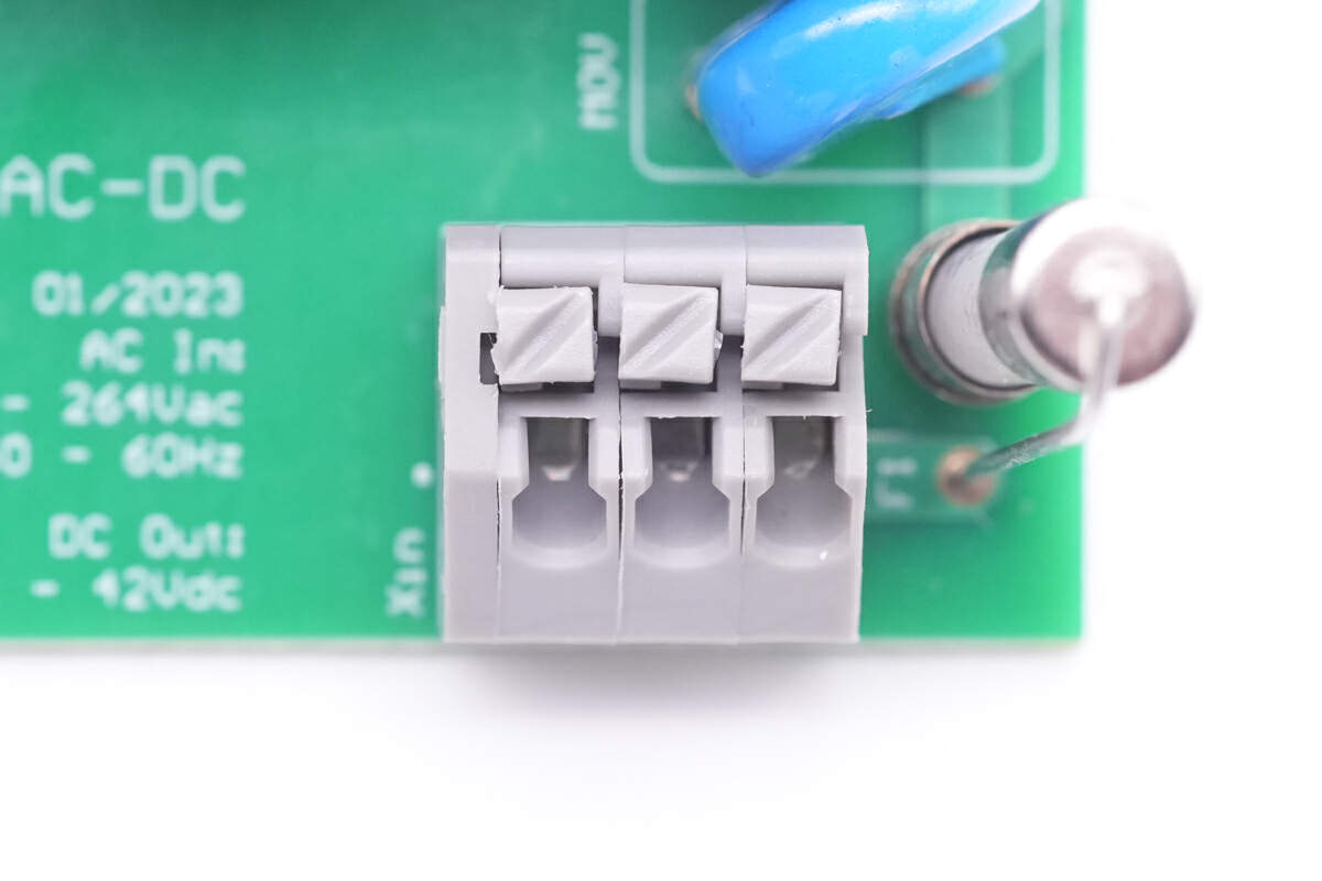
The connector is used for AC input.
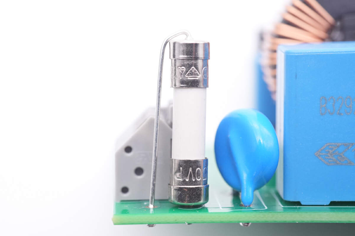
The specification of the input fuse is 2A 250V.
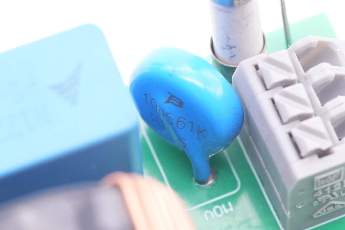
The varistor is used to absorb surge current. Model is 10D561K.
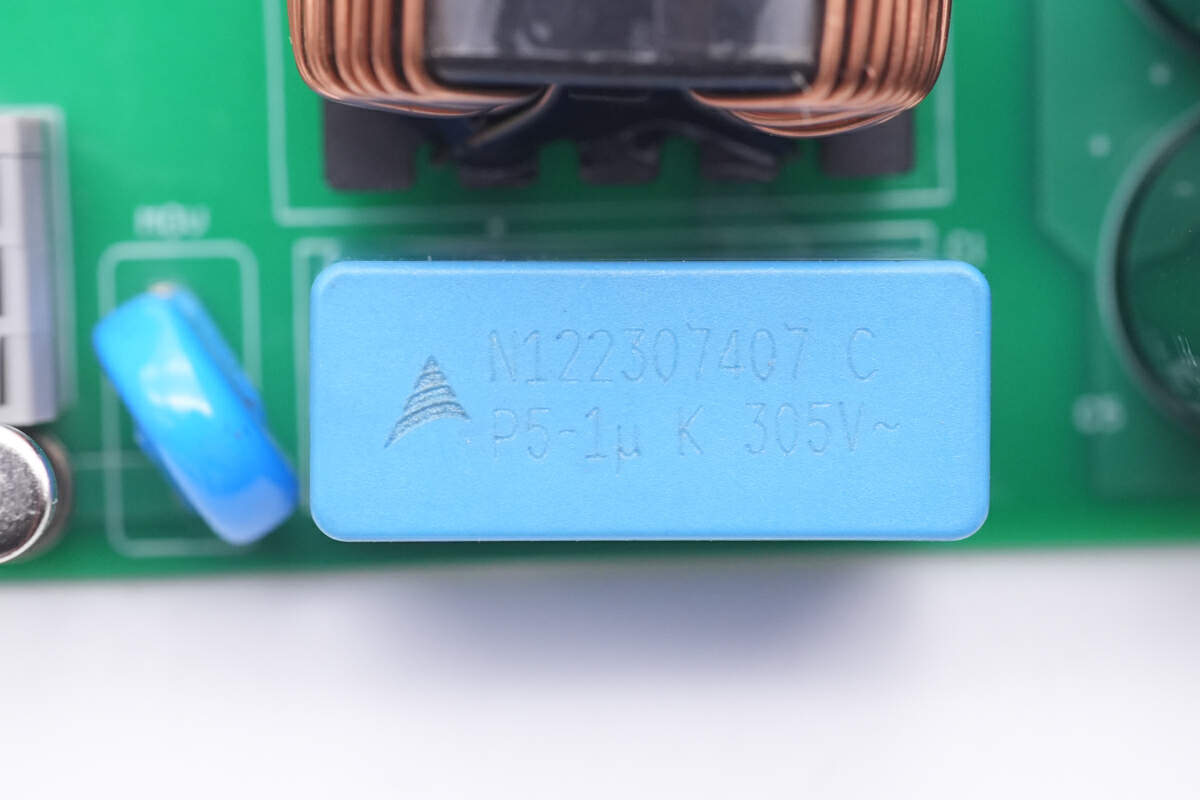
The safety X2 capacitor is from TDK. 1μF.
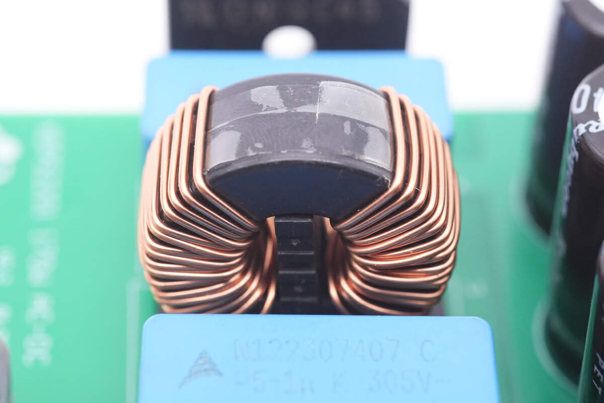
The common mode choke is wound with magnetic core.
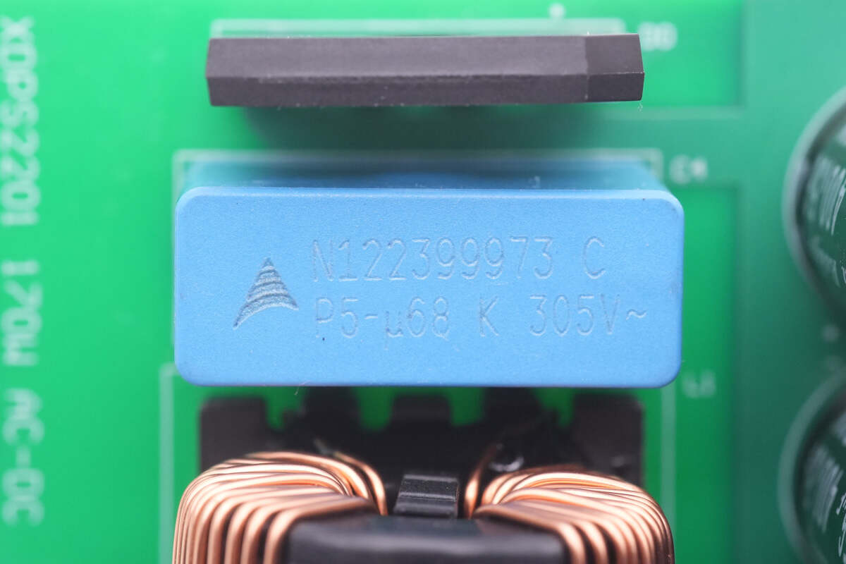
The capacity of another safety X2 capacitor is 0.68μF.
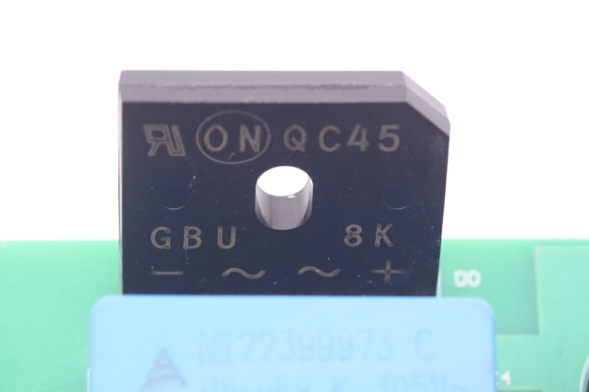
The bridge rectifier is from Onsemi. Model is GBU8K. 8A 800V.
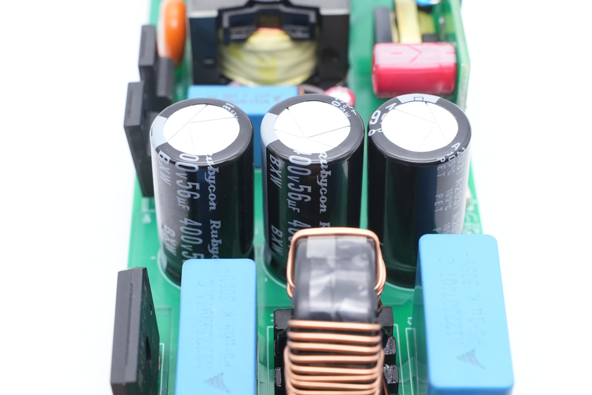
These three electrolytic capacitors for input filtering are from Rubycon and they are connected in parallel. 56μF 400V each.
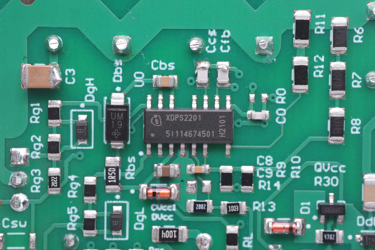
The digital hybrid flyback controller is from Infineon and adopts PG-DSO-14 package. It integrates 600V high-voltage start-up cell for fast charging. The standby power consumption is less than 75mW. Model is XDPSS2201.
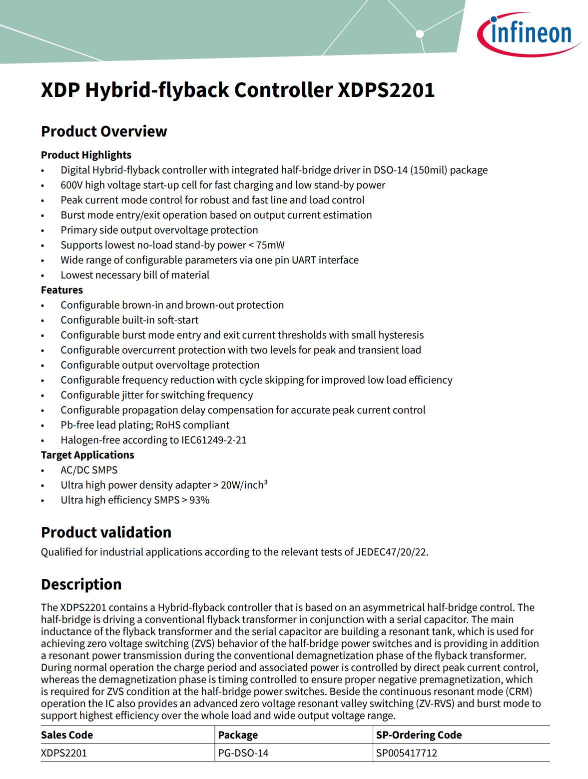
Here is all the information about the Infineon XPDS2201.
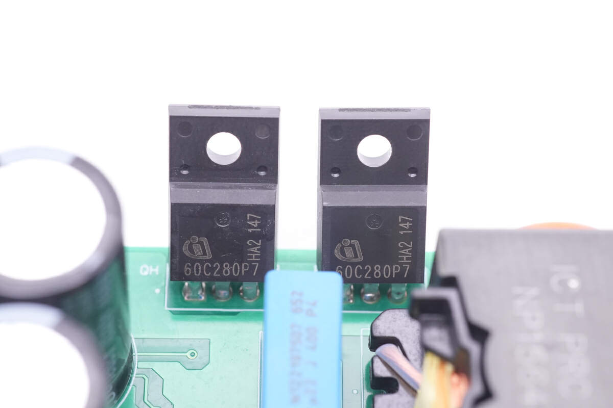
These two MOSFETs are from Infineon P7 series and adopt TO220F package. Model is IPA60R280P7S. 650V 280mΩ each.
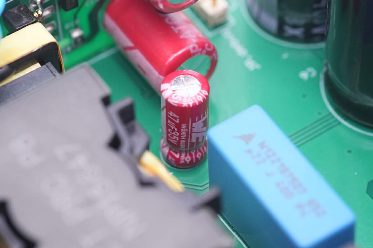
The filter capacitor that powers the master control chip is from WE. 47μF35V.
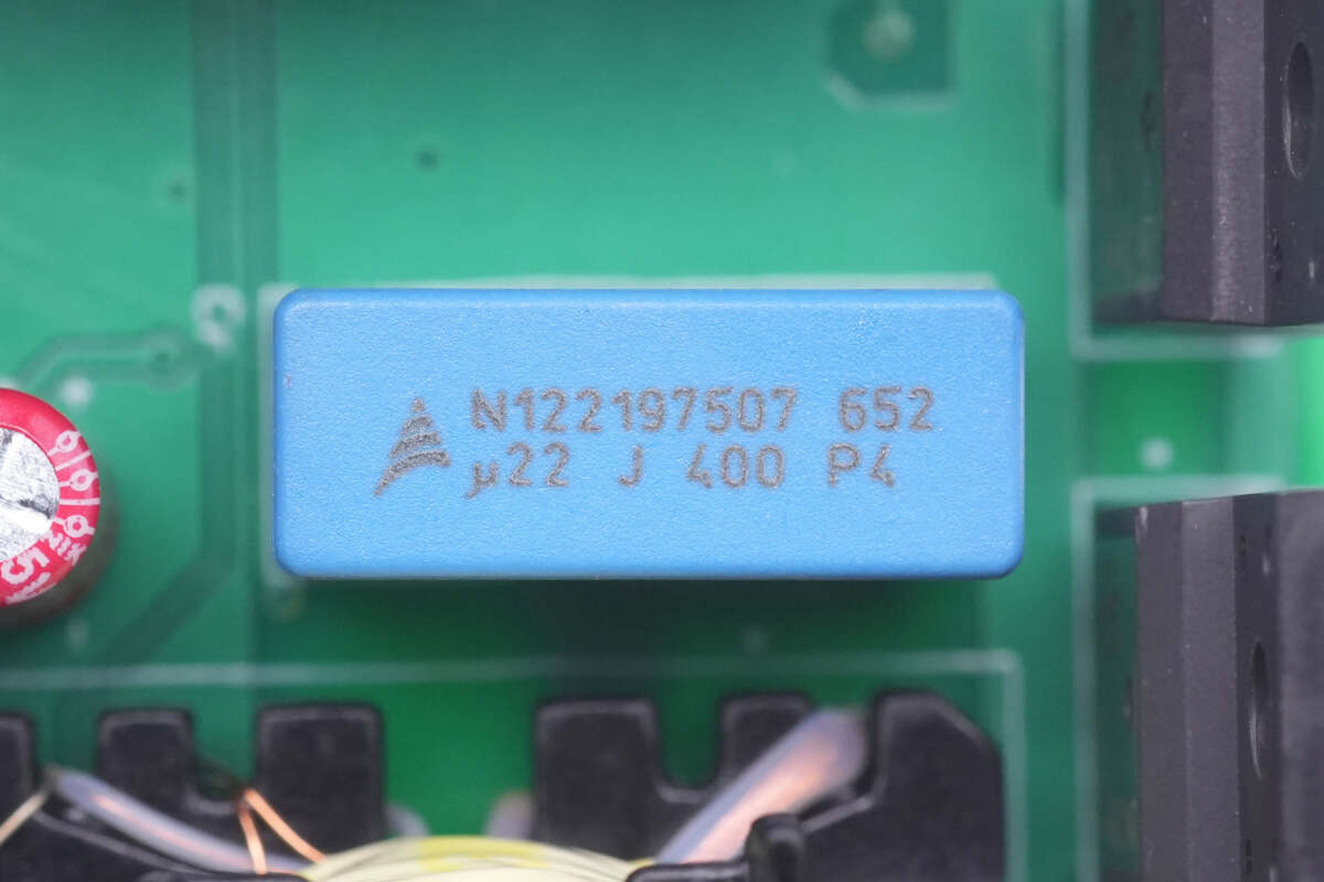
The capacity of the resonant capacitor is 0.22μF.
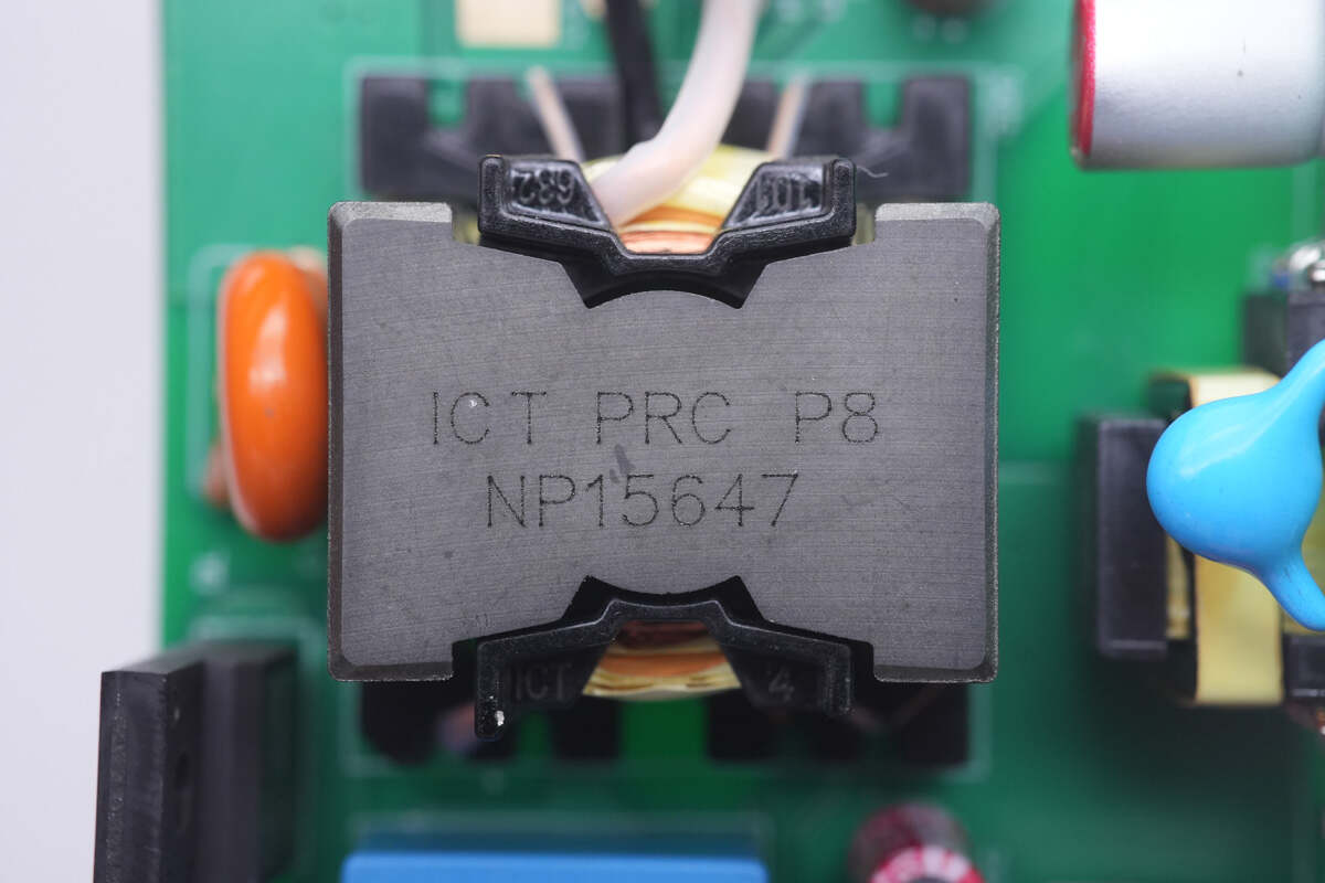
The transformer is wound with insulated wires.
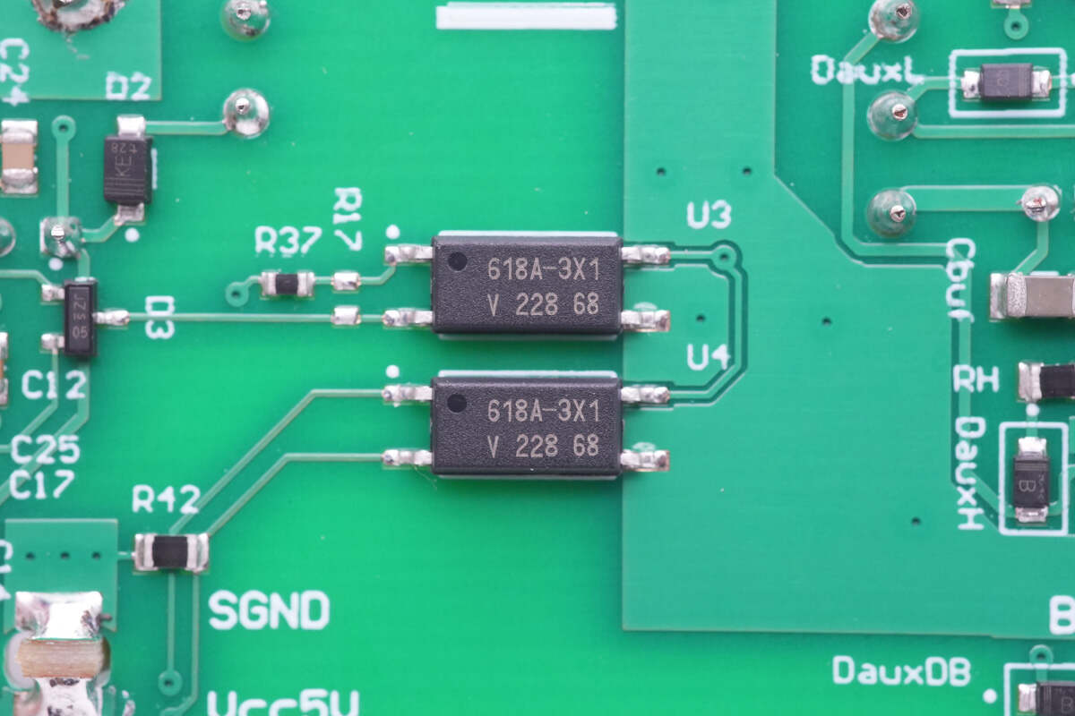
Two optocouplers are used for voltage feedback and shutdown control. Model is VOL618A.
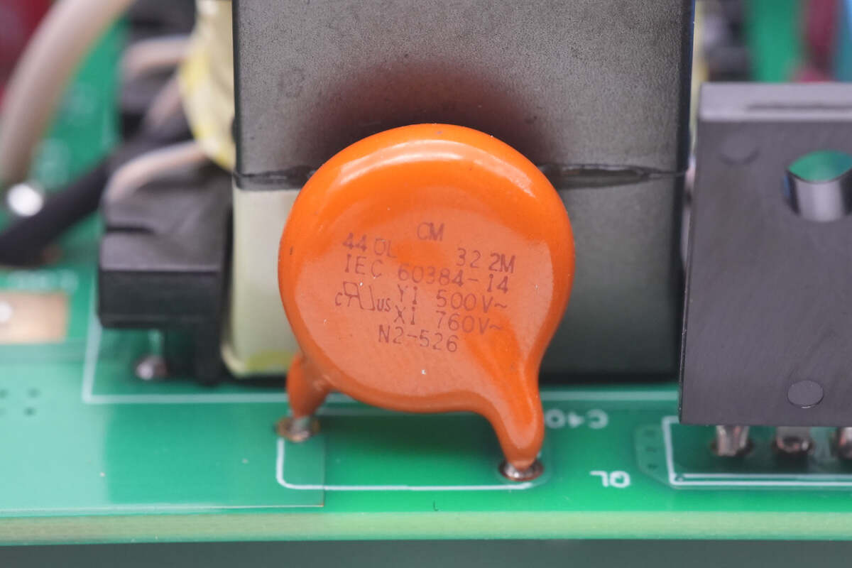
This is the orange Y capacitor.
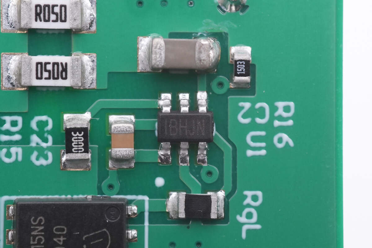
The synchronous rectifier controller marked with IBUJN is from MPS and adopts TSOT23-6 package. It supports modes of DCM, CCM, QR, ZVS, ACF (active clamp flyback), HFB (hybrid flyback). And it can drive GaN synchronous rectifiers. The frequency can reach 1MHz. Model is MP6951.
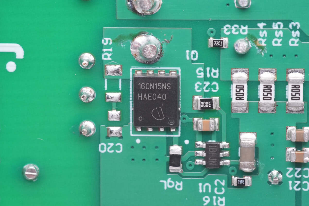
The synchronous rectifier is from Infineon and adopts SuperSO8 package. Model is BSC160N15NS5. 150V 16mΩ.
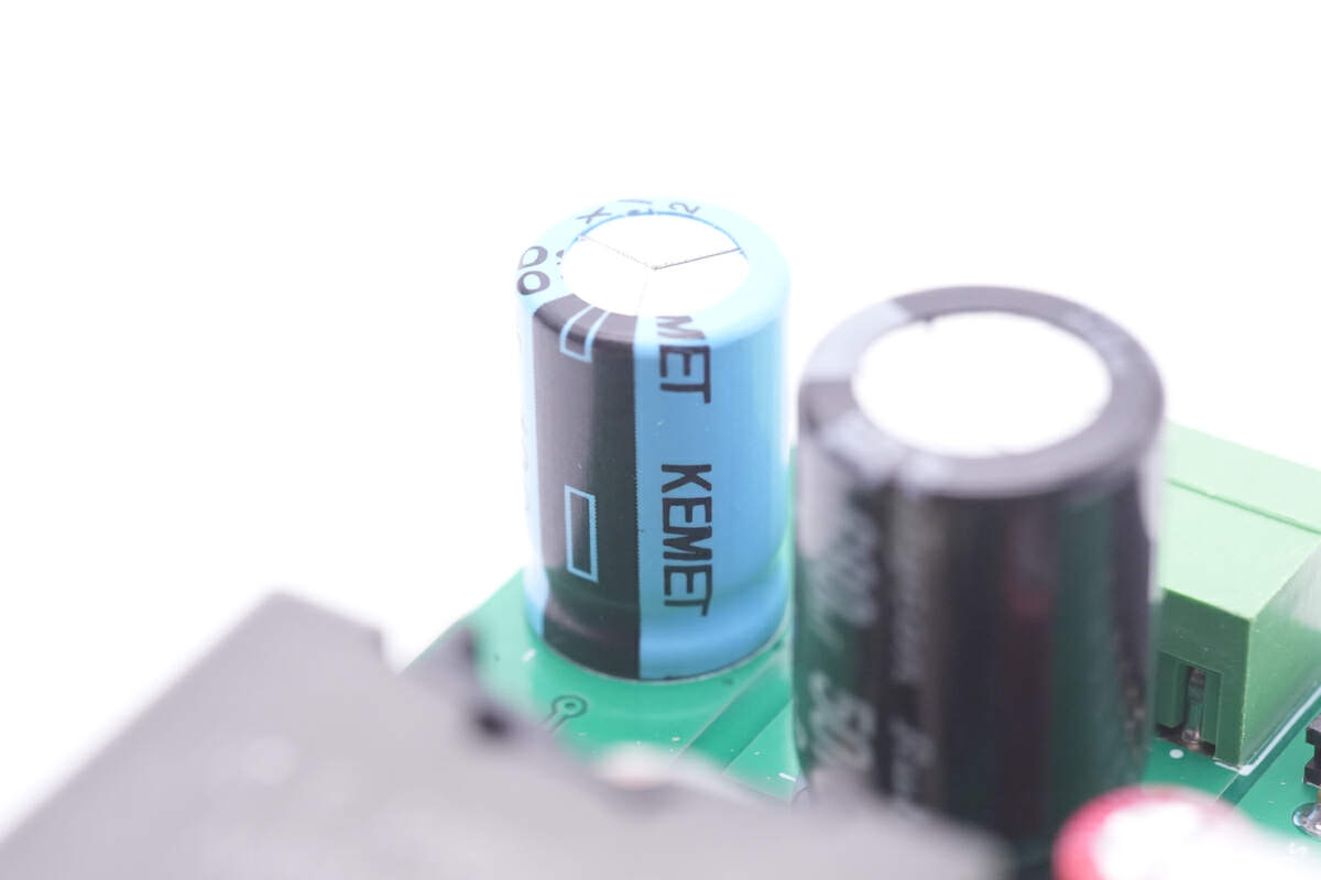
This electrolytic capacitor for output filtering is from KEMET. 100μF 50V.
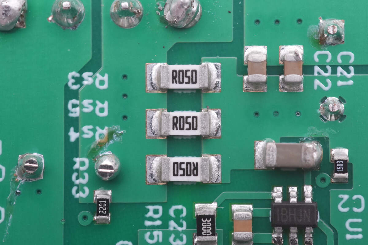
These three 50mΩ sampling resistors are connected in parallel for output current detection.
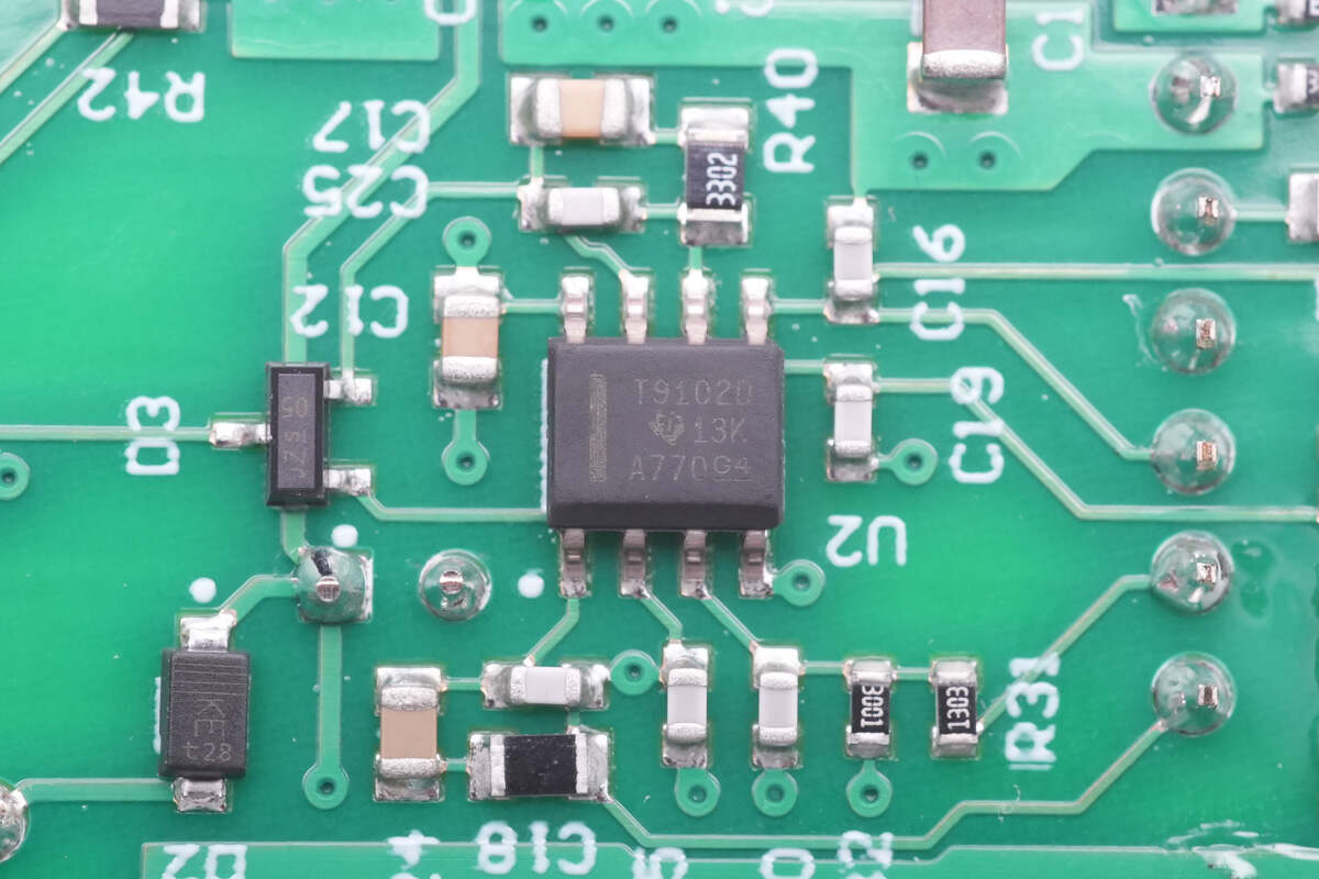
The low-power Op-Amp is from TI and supports a rail-to-rail input/output. It is used for output constant voltage and constant current control. Model is TLV9102.
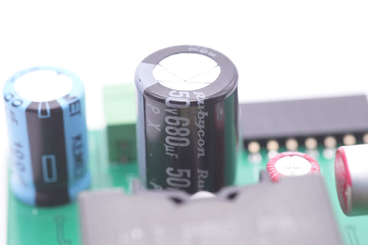
This electrolytic capacitor for output filtering is from Rubycon. 50V 680μF.
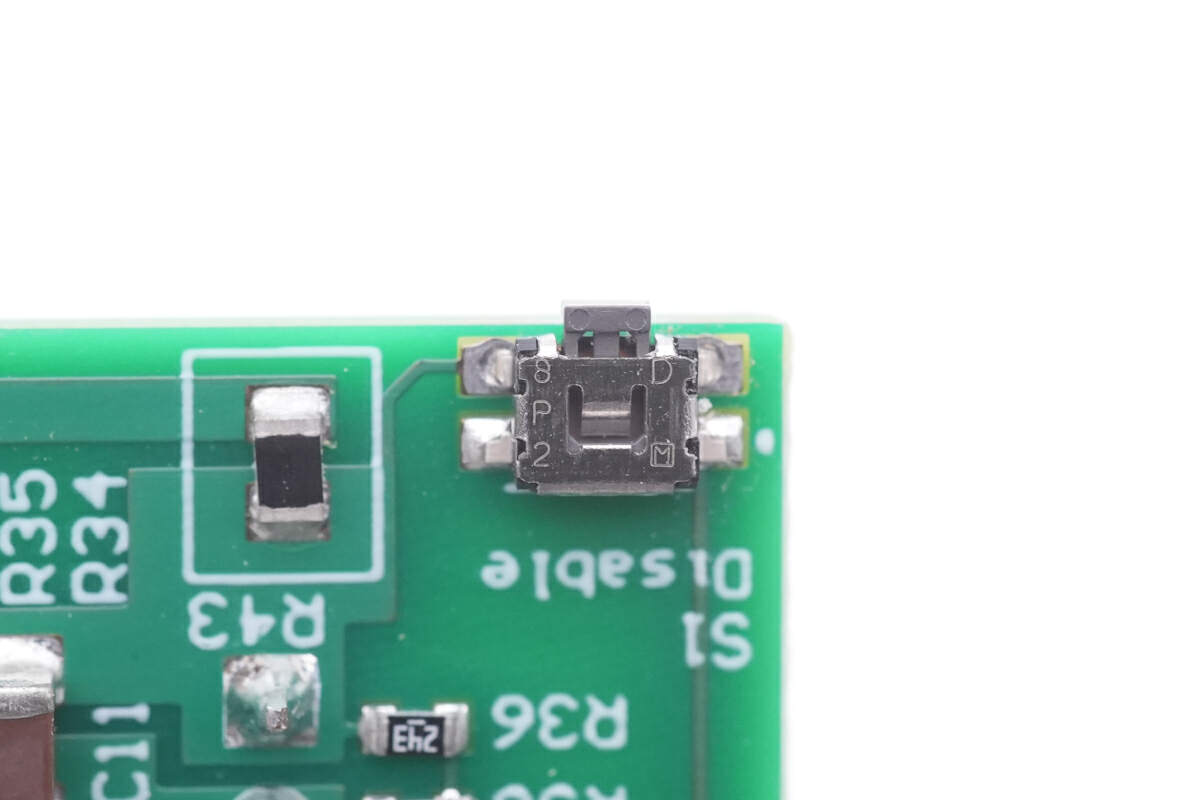
This SMD button is used for shutdown control.
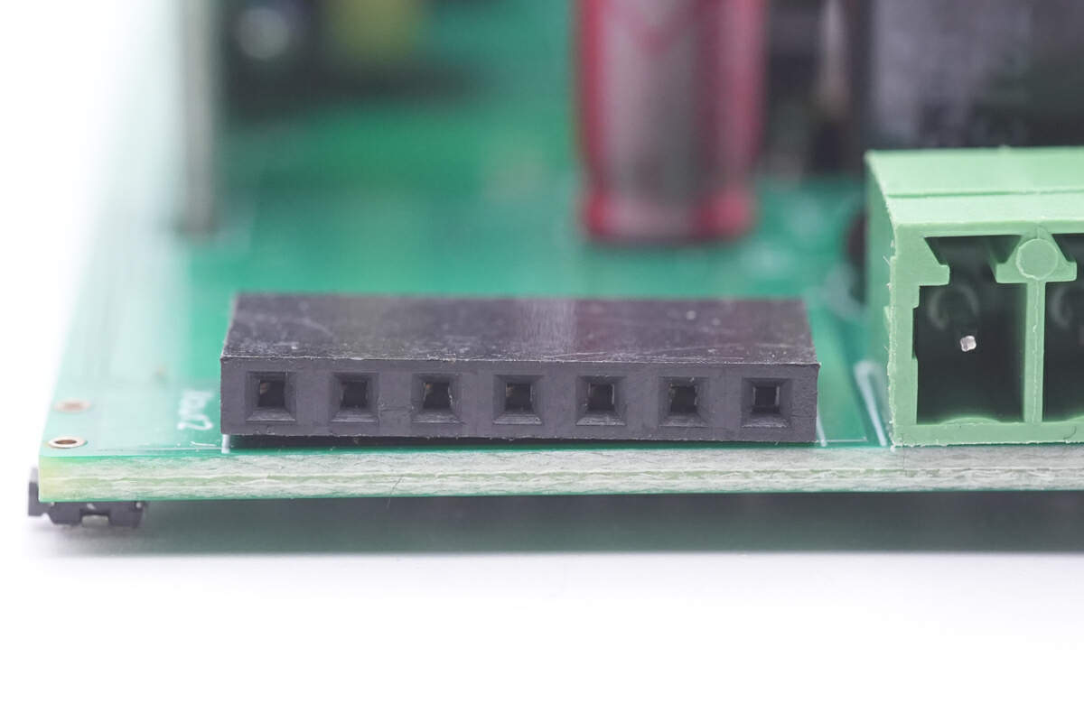
The side connector is used for current sampling, constant current and constant voltage settings, and shutdown control.
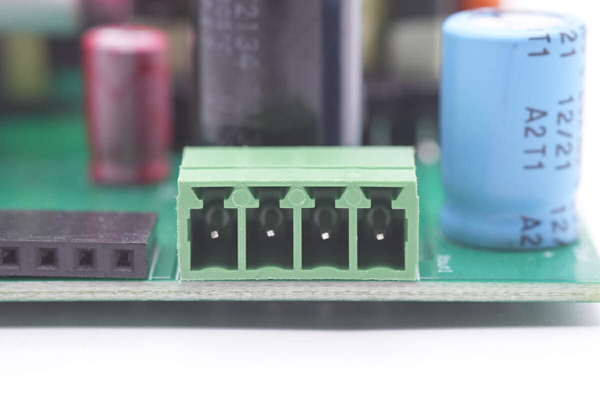
The connector is used for output.
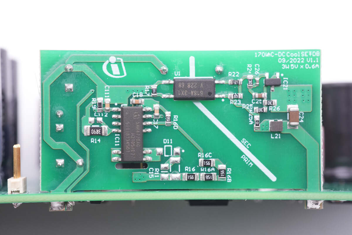
The PCB of the auxiliary power we mentioned before is used to power the control circuit.
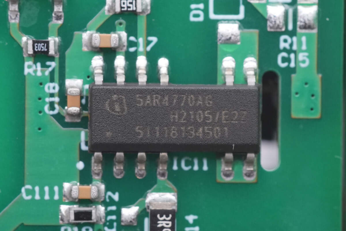
The master control chip of the auxiliary power is from Infineon CoolSET series. It integrates a MOSFET of 700V, adopts digital control, and the standby power consumption is less than 100mW. Model is CE5AR4770AG.
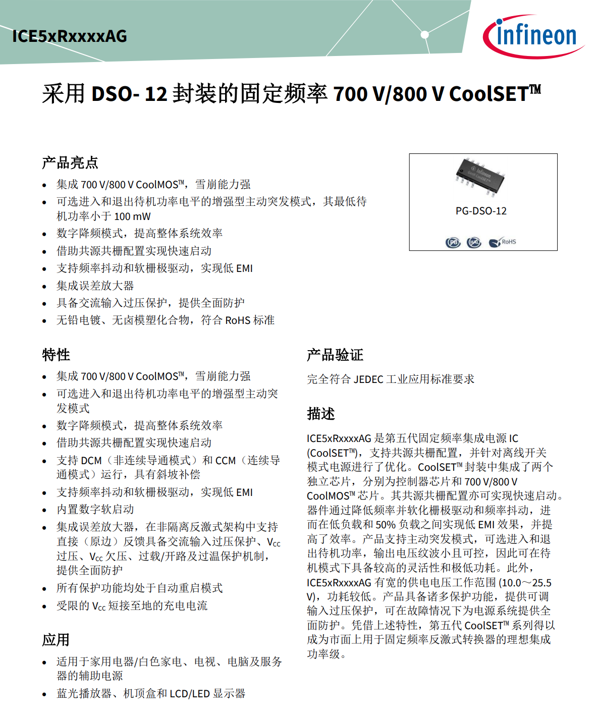
Here is the information about InfineonI CE5AR4770AG.
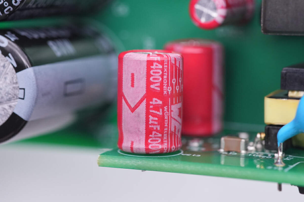
Two electrolytic capacitors for input filtering are from Würth. 4.7μF 400V.
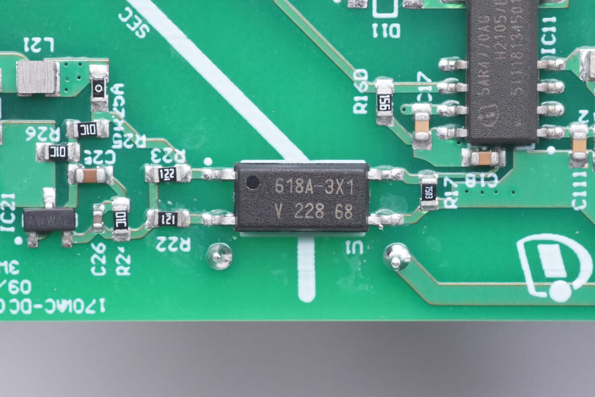
The optocoupler is used for output voltage feedback. Model is VOL618A.
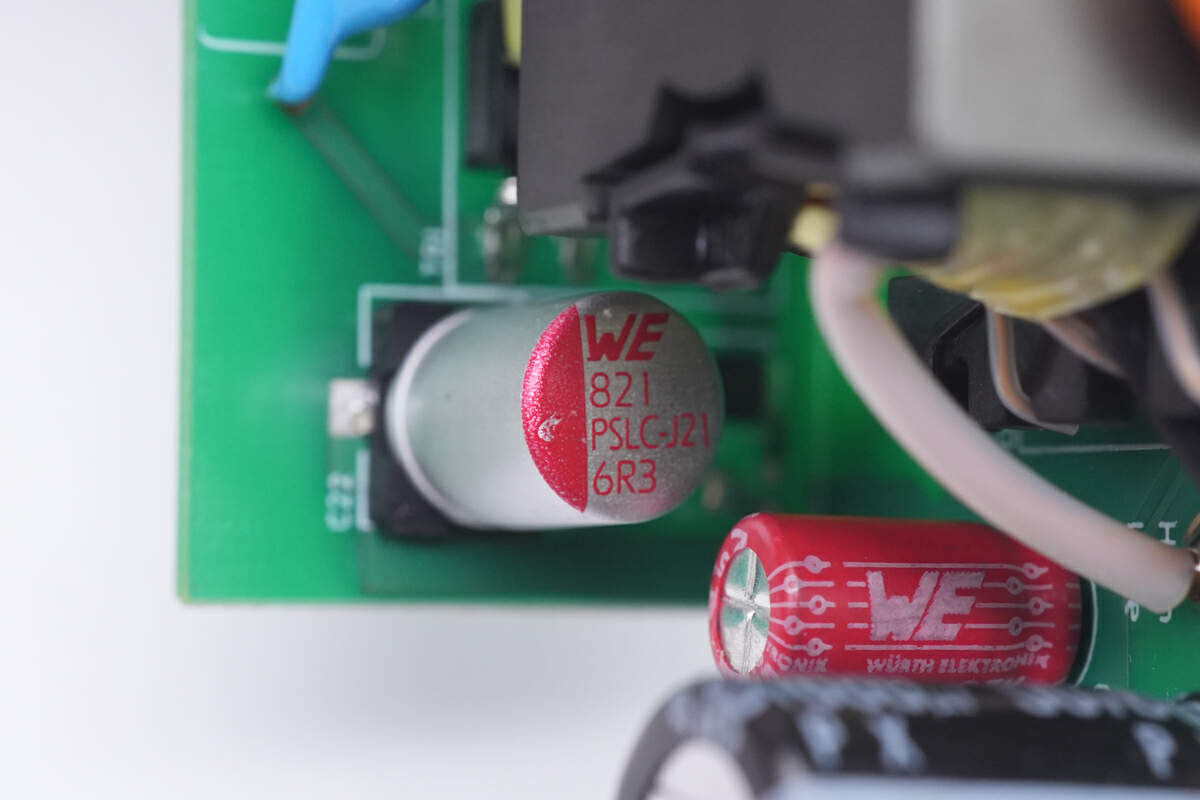
This solid capacitor for output filtering is also from Würth. It is a SMD type. 820μF 6.3V.
Summary of ChargerLAB
This XDPS2201 reference design from Infineon can output up to 170W and is suitable for the lithium-ion battery pack of 24V~36V. Due to the hybrid flyback topology, it has a high efficiency.
It consists of main power supply and auxiliary power supply. The main power supply is used to charge the eBike, and the auxiliary power supply is used to power the control circuit and other settings. The master power supply control chip and auxiliary power supply chip are both from Infineon. Except for that, some of its components come from well-known manufacturers such as Onsemi, Rubycon, and TI.
Related Articles:
1. Analysis of Innoscience 200W GaN Charger Module
2. Boost your charging speed | Analysis of PI 30W Mini PD Charger Module
3. Analysis of Southchip 33W GaN Charger Module

