Our previous review of the Samsung’s First USB-C Charger (EP-TA800) that comes with the Samsung Galaxy S10 5G reveals that the tech giant is dropping its proprietary AFC protocol and embraces USB PD 3.0 PPS as its only supported fast charging protocol. Now let's give it our teardown treatment.
I Design

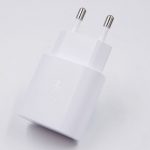
Our unit is a South Korea version with standard European plugs.

Engraved Samsung's Super Fast Charging logo.

Specifications on the back. Model: EP-TA800. Input: 100-240V~ 50/60Hz 0.7A. USB PD output: 5V/3A, 9V/2.77A. PPS output: 3.3-5.9V/3A, 3.3-11V/2.25A. Made by Solum Vina Company Limited on April 2019.

The charger's USB-C port, which supports USB PD3.0 PPS fast charging protocol.

Compared to a 1 Yuan RMB coin.

Compared to the Apple 18W USB-C charger (A1695). The EP-TA800 is longer due to its European plugs.

It weighs 51.6g (1.8oz).
II Test

Using our ChargerLAB Power-Z KT001 USB tester, it shows that the charger only supports USB PD protocol. No other protocol (including Samsung's own AFC) is supported.

PDO information reveals it is capable of USB PD charging in fixed steps at 5V/3A and 9V/2.77A, and variable PPS steps at 3.3-5.9V/3A and 3.3-11V/2.75A. That means it is a USB PD 3.0 PPS charger.
III Teardown

The charger housing is sonic welded which makes it very strong. In case you are wondering why the European plugs are longer than other plugs, well, let's take it apart more thoroughly and look at the internal structure of the plugs.

The plugs consist of a metal dome to connect the PCB and AC conductive columns, nothing special than other plugs in fact.

Taking a look at the control circuit on the back of the PCB. There is a long strip of white glue near the rectifier bridge. It adopts optocoupler feedback method with the upper part being the primary part, and the lower part being the secondary part, with isolation in the middle. The area that near the main control switch tube is hollowed out and inserted with a plastic insulation board, and the primary switch tube is glued to assist heat dissipation.

Remove the white glue and reveals the PWM chip, iW1791 from Dialog.

Detailed specifications of the Dialog iW1791.

The rectifier bridge next to the main controller IC.

The primary main control switch from Shanghai CYG Wayon, model WMO14N70C2, 700V, 0.45Ω DPAK (TO-252), which belongs to the super junction MOSFET series developed by CYG Wayon. It utilizes charge balance technology for extremely low on-resistance and low gate charge performance. It is suitable for applications which require superior power density and outstanding efficiency. Samsung's adoption of CYG Wayon's MOSFET as the main control switch in the charger of the world's first 5G mobile phone indicates that the quality of Chinese domestic power devices has reached the top international level.

Detailed specifications of the CYG Wayon WMO14N70C2.

Everlight 1018 opticalcoupler. Between the primary side and secondary side, the PCB under the optocoupler is hollowed out with a safe spacing of 6mm.

Synchronous rectifier controller iW676 from Dialog.

Detailed specifications of the Dialog iW676.

The secondary synchronous rectification MOS tube from Infineon. Beside is the USB-C port VBUS switch.

There is a Dialog iW656P USB PD protocol chip near the output port in the front of the PCB, which has passed the Qualcomm QC4+ certification.

The Dialog iW656P USB power delivery (USB PD) 3.0 interface controller resides on the secondary side of the AC/DC power supply and manages the communication between the power adapter and mobile device. It provides an extremely simplified design compared to traditional MCU-based solutions. The iW656P works with Dialog's iW1781 (45W) or iW1791 (27W) AC/DC controller chip and iW676 synchronous rectifier to achieve a power adapter design with more smaller form factor, lower cost, and higher efficiency (over 90%), using fewer external components than current solutions on the market.

VBUS switch MOS tube for USB-C port.
Now let's take a look at the front.

It can be seen that the front design of the PCBA is very compact and uses a flat panel transformer, which is offten seen in Samsung's chargers. Two primary filter electrolytic capacitors are placed horizontally to save space, and there are glues between the transformer and the electrolytic capacitor for reinforcement. The design of the PCBA overall is refined.

A fuse is placed at the input side.

2W 1.1Ω lettering.

An inductor with color rings.

A filter inductor wrapped in a heat shrinkable tube.

The four wires on the side for output are connected to the secondary side, and there is a yellow capacitor next to the transformer for powering the PWM controller IC.

The capacitor is from CapXon, 4.7μF 50V.

The longer of the two primary filter electrolytic capacitors is a 22μF 400V one from CapXon.

Another electrolytic capacitor is a 15μF 400V one from Chang.

The USB-C output port is designed with an anti-dust casing. On the left side is a Y capacitor for anti-interference, and on the right side is a solid capacitor for output filtering.

Close-up of the Y capacitor.

The output is filtered by a solid-state capacitor with a specification of 600μF 14V.

The flat panel transformer.

Remove the flat panel transformer.

There is glue injection and auxiliary heat dissipation between the transformer and the PCB, and the PCB primary side can be seen in the lower left corner.

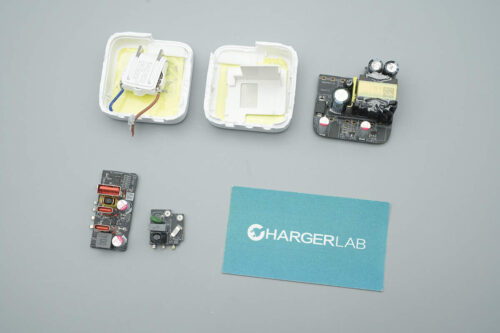
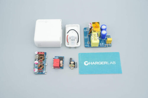
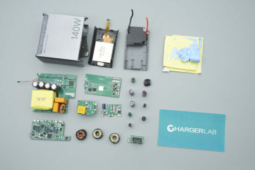
All the components.
IV Conclusion
As can be seen from our teardown, the EP-TA800 continues the refined design and quality of Samsung products. The use of the CYG Wayon's MOSFET as the main control switch in the charger of the world's first 5G mobile phone indicates that the quality of Chinese domestic power devices has reached the top international level. And the use of Dialog solution enables a design with a compact body and high efficiency.
With Apple already adopts USB PD as its only supported fast charging protocol, and now Samsung's commitment to USB PD with its first USB-C charger, the unified charging protocol of the future is clear. But for now, the perfect charger would be a USB-C PD charger which supports other existing fast charging protocols as well.
Pros:
Up to 25W USB PD 3.0 PPS charging.
Compact form factor.
High quality components.
Cons:
Supports USB PD protocol only.
Source: chongdiantou

