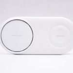
Previously we disassembled the Samsung Wireless Charger Portable Battery (EB-U1200), and recently Samsung has released a new dual-mode wireless charging product: the Samsung Wireless Charger Duo Pad (EP-P5200). This charging pad lets you wirelessly charge up to two Qi-compatible smartphones, such as a Galaxy S10, iPhone X, or Pixel 3; or a QI-compatible smartphone and smartwatch, such as the Galaxy Watch, Gear S3, or Gear Sport. Next, let's give it a teardown treatment.
I. Unboxing

Our review unit is a Chinese domestic version in white.

It comes with a AFC 25W charger.

The Samsung Wireless Charger Duo Pad has two charging areas. One on the left side (Fast Charge 2.0) which is compatible with Qi certified phones and Galaxy Buds. The other one on the right side (Fast Charge) which is compatible with Qi certified phones and other Qi products. Also, it can charge Galaxy Watch, Gear S3. Gear Sport. When you charge two mobile devices (besides the Galaxy Watch) at the same time, you cannot use fast wireless charging 2.0.
The Fast Charge 2.0 and Fast Charge feature found in the Pad Fast Charger 2.0 is compatible with Samsung Galaxy S10 and Fast Charge is compatible with Samsung Galaxy Note9, S9, S9+, Note8, S8, S8+, S7, S7 Edge, Note5, S6 Edge+ and later models of the Galaxy S and Galaxy Note series and requires a wall charger (Use AFC 25W only, EP-TA300) and USB 2.0 cable. Galaxy S6, S6 Edge, Galaxy Watch, Gear S3, Gear Sport, Galaxy Buds only support normal wireless charging, without fast charging feature.

Slides open reveals the items.

Package contents: Wireless Charger Duo Pad, wall charger (AFC 25W), USB-A to USB-C cable, user manual, and warranty card.

Wall charger model: EP-TA300. Input: 100-240v, 50-60hz, 1.0a. Output: 12v-2.1a, 5.0v-2.0a. Manufacturer: Solum Vina Company Limited. Made in Vietnam.

USB-A port on the side.

Compared to the Samsung EP-TA200 15W charger (on the left).

The included USB-A to USB-C cable.

There is a sticker on top with printed instructions: the left side can be used for phones, while the right side can be used for phones or Samsung watches.

Pilling off the sticker reveals a clean minimalist design.

Ventilation holes on the sides and bottom.

Close-up of the ventilation holes.

Specifications on the bottom.

Non-slip rubber pad on the left and right ends.

ADVANCED CHARGE 2.0 area on the left.

ADVANCED CHARGE area on the right.

USB-C port in the center.

A thickness of 18.05mm (0.71in).

Close-up of USB-C port.

Close-up.

Floating visual effect.

There are two LED indicators for two wireless charging areas respectively.

The LEDs feature a hidden design that they are not visible when they are off.

It starts charging instantly when we put the phone on top. Our Samsung Galaxy S10+ shows it gets fast charging when it is on the left of the pad.

Our Samsung Galaxy S10+ shows it gets fast charging when it is on the right of the pad.

Using ChargerLAB POWER-Z FL001Super tester, we read a power output of 21.23W (12.00V/1.78A). Both the two Samsung Galaxy S10+ are getting fast wireless charging.

Charging the Samsung Galaxy S10+ and iPhone Xs Max at the same time, our ChargerLAB POWER-Z FL001Super tester reads a power output of 16.78W (11.92V/1.41A). The Samsung Galaxy S10+ is getting fast wireless charging while the iPhone Xs Max is getting 5W normal wireless charging.
II Teardown

Removing the rubber pads on the bottom reveals several screws.

Unscrew and open the shell.

A fan occupies almost half of the internal.

A Toshiba 5V 0.31A centrifugal fan.

There are 3 sets of coil outputs on the PCB.

The input goes through two independent step-down circuits for wireless charging.

The smaller side has two separate coils, and the eight tubes are used for wireless charging. Six of the DFN2x2 packaged tubes are used for wireless charging, while the other two 3x3 are used for power switching of the coils.

The Type-C port is screwed to the housing.

Unscrew the screws for out next step.

The fan is similar to the ones used in laptops.

Vents around the wireless charging coil.

The two coils are stacked up to offer better compatibility for different devices.

An MCU controller and a wireless charging controller on the back.

A wireless charging controller with two buck and drive circuits.

Size comparison to a 1 Yuan RMB coin.

IDT IDTP9236 wireless charging master control chip on the back of the board.

Flash memory to store configs.

Drive switching circuit, as seen on our Samsung Wireless Charger Portable Battery teardown.

Another memory chip for IDTP9236.

An IC chip, function unknown.

Wireless charging drive circuit, four tubes form the H-bridge driver, and the SI7615A is used for power switching.

Another set of coil drive tubes.

DFN2x2 tubes.

SI7615A for switching the power supply of coils.

Silergy synchronous rectification step-down IC, two independent ways.

BDJAWF lettering.

Input TVS components and overvoltage protection tube.

ETEK ET9539 provides overvoltage shutdown and overcurrent protection as input protection.

2R2 step-down inductor.

The buck output goes directly to the wireless charging power stage through a 20mΩ resistor.

Type-C port from JNTC.

another IDTP9236.

Step-down IC from MPS powers the wireless charging chip.

ABOV MCU for wireless charging protection and other functions.

A Samsung custom chip.

A switch.

Date: April 4th, 2019.

Two LED Indicators.

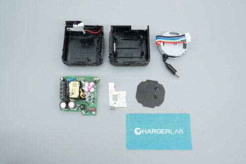
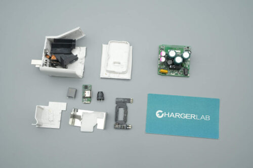
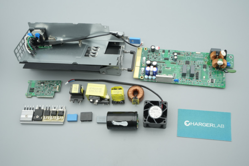
All the components.
III ChargerLAB conclusion
The Samsung Wireless Charger Duo Pad offers all-in-one wireless charging solution for your phones and Samsung watches. It has a minimalistic design with an active cooling fan inside to take away the heat generated by fast wireless charging. We are also very impressed by the high-quality components and excellent craftsmanship of this wireless charging pad.
Note: ChargerLAB is reader-supported. Our editors independently research, test, and recommend the best products. We may earn commissions on purchases made from links on our site.
Source: chongdiantou

